EP3026701B1 - Leistungsmodul und herstellungsverfahren davon - Google Patents
Leistungsmodul und herstellungsverfahren davon Download PDFInfo
- Publication number
- EP3026701B1 EP3026701B1 EP14829390.5A EP14829390A EP3026701B1 EP 3026701 B1 EP3026701 B1 EP 3026701B1 EP 14829390 A EP14829390 A EP 14829390A EP 3026701 B1 EP3026701 B1 EP 3026701B1
- Authority
- EP
- European Patent Office
- Prior art keywords
- power module
- insulating layer
- module according
- groove
- leadframe
- Prior art date
- Legal status (The legal status is an assumption and is not a legal conclusion. Google has not performed a legal analysis and makes no representation as to the accuracy of the status listed.)
- Active
Links
Images



Classifications
-
- H—ELECTRICITY
- H10—SEMICONDUCTOR DEVICES; ELECTRIC SOLID-STATE DEVICES NOT OTHERWISE PROVIDED FOR
- H10W—GENERIC PACKAGES, INTERCONNECTIONS, CONNECTORS OR OTHER CONSTRUCTIONAL DETAILS OF DEVICES COVERED BY CLASS H10
- H10W70/00—Package substrates; Interposers; Redistribution layers [RDL]
- H10W70/40—Leadframes
- H10W70/421—Shapes or dispositions
- H10W70/424—Cross-sectional shapes
- H10W70/427—Bent parts
-
- H—ELECTRICITY
- H10—SEMICONDUCTOR DEVICES; ELECTRIC SOLID-STATE DEVICES NOT OTHERWISE PROVIDED FOR
- H10W—GENERIC PACKAGES, INTERCONNECTIONS, CONNECTORS OR OTHER CONSTRUCTIONAL DETAILS OF DEVICES COVERED BY CLASS H10
- H10W40/00—Arrangements for thermal protection or thermal control
- H10W40/10—Arrangements for heating
-
- H—ELECTRICITY
- H10—SEMICONDUCTOR DEVICES; ELECTRIC SOLID-STATE DEVICES NOT OTHERWISE PROVIDED FOR
- H10W—GENERIC PACKAGES, INTERCONNECTIONS, CONNECTORS OR OTHER CONSTRUCTIONAL DETAILS OF DEVICES COVERED BY CLASS H10
- H10W40/00—Arrangements for thermal protection or thermal control
- H10W40/70—Fillings or auxiliary members in containers or in encapsulations for thermal protection or control
-
- H—ELECTRICITY
- H10—SEMICONDUCTOR DEVICES; ELECTRIC SOLID-STATE DEVICES NOT OTHERWISE PROVIDED FOR
- H10W—GENERIC PACKAGES, INTERCONNECTIONS, CONNECTORS OR OTHER CONSTRUCTIONAL DETAILS OF DEVICES COVERED BY CLASS H10
- H10W70/00—Package substrates; Interposers; Redistribution layers [RDL]
- H10W70/01—Manufacture or treatment
- H10W70/04—Manufacture or treatment of leadframes
- H10W70/048—Mechanical treatments, e.g. punching, cutting, deforming or cold welding
-
- H—ELECTRICITY
- H10—SEMICONDUCTOR DEVICES; ELECTRIC SOLID-STATE DEVICES NOT OTHERWISE PROVIDED FOR
- H10W—GENERIC PACKAGES, INTERCONNECTIONS, CONNECTORS OR OTHER CONSTRUCTIONAL DETAILS OF DEVICES COVERED BY CLASS H10
- H10W70/00—Package substrates; Interposers; Redistribution layers [RDL]
- H10W70/40—Leadframes
- H10W70/421—Shapes or dispositions
- H10W70/424—Cross-sectional shapes
-
- H—ELECTRICITY
- H10—SEMICONDUCTOR DEVICES; ELECTRIC SOLID-STATE DEVICES NOT OTHERWISE PROVIDED FOR
- H10W—GENERIC PACKAGES, INTERCONNECTIONS, CONNECTORS OR OTHER CONSTRUCTIONAL DETAILS OF DEVICES COVERED BY CLASS H10
- H10W70/00—Package substrates; Interposers; Redistribution layers [RDL]
- H10W70/40—Leadframes
- H10W70/481—Leadframes for devices being provided for in groups H10D8/00 - H10D48/00
-
- H—ELECTRICITY
- H10—SEMICONDUCTOR DEVICES; ELECTRIC SOLID-STATE DEVICES NOT OTHERWISE PROVIDED FOR
- H10W—GENERIC PACKAGES, INTERCONNECTIONS, CONNECTORS OR OTHER CONSTRUCTIONAL DETAILS OF DEVICES COVERED BY CLASS H10
- H10W74/00—Encapsulations, e.g. protective coatings
- H10W74/01—Manufacture or treatment
- H10W74/012—Manufacture or treatment of encapsulations on active surfaces of flip-chip devices, e.g. forming underfills
-
- H—ELECTRICITY
- H10—SEMICONDUCTOR DEVICES; ELECTRIC SOLID-STATE DEVICES NOT OTHERWISE PROVIDED FOR
- H10W—GENERIC PACKAGES, INTERCONNECTIONS, CONNECTORS OR OTHER CONSTRUCTIONAL DETAILS OF DEVICES COVERED BY CLASS H10
- H10W74/00—Encapsulations, e.g. protective coatings
- H10W74/10—Encapsulations, e.g. protective coatings characterised by their shape or disposition
- H10W74/111—Encapsulations, e.g. protective coatings characterised by their shape or disposition the semiconductor body being completely enclosed
- H10W74/121—Encapsulations, e.g. protective coatings characterised by their shape or disposition the semiconductor body being completely enclosed by multiple encapsulations, e.g. by a thin protective coating and a thick encapsulation
-
- H—ELECTRICITY
- H10—SEMICONDUCTOR DEVICES; ELECTRIC SOLID-STATE DEVICES NOT OTHERWISE PROVIDED FOR
- H10W—GENERIC PACKAGES, INTERCONNECTIONS, CONNECTORS OR OTHER CONSTRUCTIONAL DETAILS OF DEVICES COVERED BY CLASS H10
- H10W74/00—Encapsulations, e.g. protective coatings
- H10W74/10—Encapsulations, e.g. protective coatings characterised by their shape or disposition
- H10W74/15—Encapsulations, e.g. protective coatings characterised by their shape or disposition on active surfaces of flip-chip devices, e.g. underfills
-
- H—ELECTRICITY
- H10—SEMICONDUCTOR DEVICES; ELECTRIC SOLID-STATE DEVICES NOT OTHERWISE PROVIDED FOR
- H10W—GENERIC PACKAGES, INTERCONNECTIONS, CONNECTORS OR OTHER CONSTRUCTIONAL DETAILS OF DEVICES COVERED BY CLASS H10
- H10W72/00—Interconnections or connectors in packages
- H10W72/50—Bond wires
- H10W72/531—Shapes of wire connectors
- H10W72/5363—Shapes of wire connectors the connected ends being wedge-shaped
-
- H—ELECTRICITY
- H10—SEMICONDUCTOR DEVICES; ELECTRIC SOLID-STATE DEVICES NOT OTHERWISE PROVIDED FOR
- H10W—GENERIC PACKAGES, INTERCONNECTIONS, CONNECTORS OR OTHER CONSTRUCTIONAL DETAILS OF DEVICES COVERED BY CLASS H10
- H10W72/00—Interconnections or connectors in packages
- H10W72/851—Dispositions of multiple connectors or interconnections
- H10W72/874—On different surfaces
- H10W72/884—Die-attach connectors and bond wires
-
- H—ELECTRICITY
- H10—SEMICONDUCTOR DEVICES; ELECTRIC SOLID-STATE DEVICES NOT OTHERWISE PROVIDED FOR
- H10W—GENERIC PACKAGES, INTERCONNECTIONS, CONNECTORS OR OTHER CONSTRUCTIONAL DETAILS OF DEVICES COVERED BY CLASS H10
- H10W74/00—Encapsulations, e.g. protective coatings
- H10W74/10—Encapsulations, e.g. protective coatings characterised by their shape or disposition
- H10W74/111—Encapsulations, e.g. protective coatings characterised by their shape or disposition the semiconductor body being completely enclosed
-
- H—ELECTRICITY
- H10—SEMICONDUCTOR DEVICES; ELECTRIC SOLID-STATE DEVICES NOT OTHERWISE PROVIDED FOR
- H10W—GENERIC PACKAGES, INTERCONNECTIONS, CONNECTORS OR OTHER CONSTRUCTIONAL DETAILS OF DEVICES COVERED BY CLASS H10
- H10W90/00—Package configurations
- H10W90/701—Package configurations characterised by the relative positions of pads or connectors relative to package parts
- H10W90/731—Package configurations characterised by the relative positions of pads or connectors relative to package parts of die-attach connectors
- H10W90/736—Package configurations characterised by the relative positions of pads or connectors relative to package parts of die-attach connectors between a chip and a stacked lead frame, conducting package substrate or heat sink
-
- H—ELECTRICITY
- H10—SEMICONDUCTOR DEVICES; ELECTRIC SOLID-STATE DEVICES NOT OTHERWISE PROVIDED FOR
- H10W—GENERIC PACKAGES, INTERCONNECTIONS, CONNECTORS OR OTHER CONSTRUCTIONAL DETAILS OF DEVICES COVERED BY CLASS H10
- H10W90/00—Package configurations
- H10W90/701—Package configurations characterised by the relative positions of pads or connectors relative to package parts
- H10W90/751—Package configurations characterised by the relative positions of pads or connectors relative to package parts of bond wires
- H10W90/756—Package configurations characterised by the relative positions of pads or connectors relative to package parts of bond wires between a chip and a stacked lead frame, conducting package substrate or heat sink
Definitions
- the present invention described herein relates to a power module and a fabrication method for such a power module.
- Document JP 2001 118961 A relates to a resin-sealed power semiconductor device, and a method of manufacturing the same.
- a semiconductor pellet is fixed on the one main surface of a leadframe, a heat dissipating surface is formed on the other main surface, the semiconductor pellet is sealed up with resin so as to expose the heat dissipating surface.
- a resin package is formed by making the exposed heat dissipating surface nearly flush with the lower surface of sealing resin which surrounds the heat dissipating surface.
- a resin film which is high in thermal conductivity and electric insulation properties is bonded to the heat dissipating surface and the lower surface of the sealing resin, by which the cost of sealing resin can be lessened, the maintenance cost of a molding die can be reduced, and transfer molding conditions can be easily controlled.
- an insulating layer and a leadframe are contacted with each other on a flat surface. If external force is applied thereon in such a state where the insulating layer and the metal layer are contacted with each other on the flat surface, the insulating layer and the metal layer may be deviated (displaced) from each other, thereby causing insulation failure. Moreover, if the insulating layer and the metal layer are deviated from each other and thereby a gap is formed therebetween, a thermal resistance of the module may be increased. Thereby, since it becomes impossible to cool the semiconductor device as designed, there will be generated thermal run away of the semiconductor device, thermal deterioration of bonding layers, e.g. a solder layer, and fusing of bonding wires.
- bonding layers e.g. a solder layer
- the object of the present invention is to provide a power module with improved reliability so that an insulating layer and a metal layer may be hardly deviated from each other even if external force is applied thereon; and a fabrication method for such a power module.
- a power module comprising: an insulating layer; a metal layer disposed on the insulating layer; a semiconductor chip disposed on the metal layer; and a mold resin formed so as to cover the semiconductor chip and at least a part of the metal layer, wherein a groove into which a part of the insulating layer is inserted is formed on a surface of the metal layer facing the insulating layer.
- a fabrication method for a power module comprising: forming a groove on a bottom surface of a leadframe; bonding a semiconductor chip to the leadframe with a conductive bonding material; electrically connecting the semiconductor chip and the leadframe to each other using a connecting member; disposing the leadframe on a metallic mold and then forming an insulating layer on a bottom surface of the leadframe, the insulating layer formed so as to be inserted into the bottom surface of the leadframe; and after curing the insulating layer, closing the metallic mold, and then pouring a mold resin therein in order to mold the leadframe, the conductive bonding material, the semiconductor chip, and the connecting member.
- a power module with improved reliability so that the insulating layer and the metal layer may be hardly deviated from each other even if external force is applied thereon; and a fabrication method for such a power module.
- the embodiment described hereinafter merely exemplifies the device and method for materializing the technical idea of the present invention; and the embodiment of the present invention does not specify the material, shape, structure, placement, etc. of each component part as the following.
- FIG. 1 A schematic cross-sectional structure of a power module 20a according to a comparative example is illustrated as shown in Fig. 1 .
- a semiconductor chip 3 is bonded with a solder 2 on a leadframe 1.
- the semiconductor chip 3 and a leadframe 5 are electrically connected to each other with an aluminum wire 4.
- the leadframe 1 and the leadframe 5 are disposed on a metallic mold (not shown), and an insulating layer 7 is formed on a surface of the leadframes 1 and 5 (hereafter referred to as a "bottom surface") opposite to a surface on which the semiconductor chip 3 is mounted.
- the metallic mold is closed and then a mold resin 6 is poured therein, and thereby the power module 20a molded with the mold resin 6 can be formed.
- FIG. 2 A schematic cross-sectional structure of another power module 20b according to the comparative example is illustrated as shown in Fig. 2 .
- Fig. 2 there may be adopted a structure of bonding a metallic plate 8 on a bottom surface of the insulating layer 7.
- the insulating layer 7 is covered with the metallic plate 8, and thereby it can prevent from an externally caused crack.
- the configuration of other portions is the same as that of the power module 20a.
- FIG. 3 A schematic cross-sectional structure showing a usage example of the power module 20a shown in Fig. 1 is illustrated as shown in Fig. 3
- a schematic cross-sectional structure showing a usage example of the power module 20b shown in Fig. 2 is illustrated as shown in Fig. 4 .
- the power modules 20a and 20b according to the comparative example are used by being screwed into a heat sink 10 via a liquid thermal compound 9.
- the insulating layer 7 and the leadframes (metal layers) 1, 5 are contacted with each other on a flat surface. If external force is applied thereon in such a state where the insulating layer 7 and the metal layers 1, 5 are contacted with each other on a flat surface, the insulating layer 7 and the metal layers 1, 5 may be deviated (displaced) from each other, thereby causing insulation failure. Moreover, if the insulating layer 7 and the metal layers 1, 5 are deviated from each other and thereby a gap is formed therebetween, a thermal resistance of the power module (20a, 20b) may be increased. Thereby, since it becomes impossible to cool the semiconductor device as designed, there will be generated thermal run away of the semiconductor device, thermal deterioration of bonding layers, e.g. a solder 2, and fusing of the aluminum wire 4.
- bonding layers e.g. a solder 2
- the thermal compound 9 is liquid, time and effort are required in work for coating. Moreover, the thermal compound 9 is also hardly treated since it is necessary to be coated uniformly and thinly. Furthermore, the whole of the power module (20a, 20b) becomes deformed by warping and restoring in a repetition of cooling and heating due to operating environments, and thereby the liquid thermal compound 9 may be gradually pushed out (pumped out) therefrom. If the thermal compound 9 is pumped out therefrom, a gap may be generated between a bottom surface of the power module (20a, 20b) and the heat sink 10, and thereby a thermal resistance of the portion where the gap is generated will be increased.
- a power module 20 includes: an insulating layer 7; leadframes (metal layers) 1, 5 respectively disposed on the insulating layer 7; and a semiconductor chip 3 disposed on the leadframe 1, wherein a groove 11 into which a part of the insulating layer 7 is inserted is formed on a surface of the leadframes 1, 5 facing (opposed to) the insulating layer 7.
- the groove 11 may also be formed outside a region to which a heat generated from the semiconductor chip 3 is conducted.
- an angle between the semiconductor chip 3 and the groove 11 may be equal to or less than 45 degrees.
- the groove 11 may be formed only outside the region to which the heat generated from the semiconductor chip 3 is conducted.
- a cross-sectional shape of the groove 11 may be at least one shape selected from the group consist of a rectangle shape, a semicircle shape, a semi-ellipse shape, triangular shape, and a wedge shape.
- the groove 11 may be formed along in one direction or may be formed in a lattice-like shape.
- a surface roughening process may be applied on a surface of the leadframes 1, 5 facing the insulating layer 7.
- the insulating layer 7 may be formed of a material(s) softer than the leadframes 1, 5.
- a hardness of the insulating layer 7 may be softer than A40 in durometer hardness.
- the insulating layer 7 may be formed of an organic material(s).
- the insulating layer 7 may be formed of a silicone based resin(s).
- the insulating layer 7 may be filled up with a high thermally-conductive filler.
- the filler may be at least one selected from the group consist of aluminium oxide, silicon oxide, aluminum nitride, silicon nitride, boron nitride, beryllia, and magnesia.
- the insulating layer 7 may be formed before the semiconductor chip 3 is molded with a mold resin 6.
- an edge part of the insulating layer 7 may be intervened between the mold resin 6 and the leadframes 1, 5.
- the insulating layer 7 may be formed after the semiconductor chip 3 is molded with the mold resin 6.
- the mold resin 6 and the leadframes 1, 5 may be formed so as to be flush with each other.
- the groove 11 into which a part of the insulating layer 7 is inserted is formed in the surface of the leadframes 1, 5 facing (opposed to) the insulating layer 7, in the power module 20 according to the example.
- a flexible resin (organic material) is used for the insulating layer 7.
- the flexible resin is preferably a material(s) softer than the leadframes 1, 5, and is also preferably a resin softer than A40 in durometer hardness (e.g., silicone resin, etc.).
- the resin used for the insulating layer 7 is filled up with a high thermally-conductive filler of approximately 1 to 20 W/mK degrees, for example.
- a filler aluminium oxide, silicon oxide, aluminum nitride, silicon nitride, boron nitride, beryllia, magnesia, etc. can be used.
- the insulating layer 7 since the insulating layer 7 is tightly insert in the groove 11 by using the flexible resin for the insulating layer 7, the insulating layer 7 can be strongly bonded to the leadframes 1 and 5 without increasing the thermal resistance (anchor effect). Moreover, since the insulating layer 7 is sufficiently compatible with the surface of the heat sink 10 due to the flexibility thereof, it becomes unnecessary to coat the liquid thermal compound 9 between the bottom surface of the power module 20 and the heat sink 10 as in the case of the comparative example.
- the groove 11 is formed outside a region extended in downward direction by only the angle C from a bottom head of the solder 2. Since a heat generated from the semiconductor chip 3 is conducted by being spread at approximately 45 degrees, it is preferable to set the angle C to be equal to or less than 45 degrees. Accordingly, since no groove 11 is formed in a region to which the heat is conducted, a defect due to increase of the thermal resistance can be avoided, thereby improving the reliability thereof.
- FIG. 6 A schematic planar structure showing a usage example of the power module 20 according to the example is illustrated as shown in Fig. 6 .
- the leadframes 1, 5 are respectively screwed into the heat sink 10 with screws 61, 62. Needless to say, a position to be screwed or the number of the screws can be appropriately modified. According to such a configuration, even if a flexible resin is used for the insulating layer 7, the power module 20 is strongly joined to the heat sink 10.
- FIG. 7 A schematic cross-sectional structure taken in the line I-I shown in Fig. 5 is illustrated as shown in Fig. 7 .
- a plurality of the grooves 11 may be formed in a vertical direction.
- the vertical direction used herein is a short-side direction of the power module 20.
- a bonding strength between the insulating layer 7 and the metal layers 1, 5 can be improved against external force applied in particular on a long-side direction of the power module 20.
- FIG. 8 Another schematic cross-sectional structure taken in the line I-I shown in Fig. 5 is illustrated as shown in Fig. 8 .
- a plurality of the grooves 11 may be formed in a horizontal direction.
- the horizontal direction used herein is a long-side direction of the power module 20.
- a bonding strength between the insulating layer 7 and the metal layers 1, 5 can be improved against external force applied in particular on the short-side direction of the power module 20.
- FIG. 9 Still another schematic cross-sectional structure taken in the line I-I shown in Fig. 5 is illustrated as shown in Fig. 9 .
- the groove 11 may be formed in a lattice-like shape as shown in Fig. 9 .
- the bonding strength between the insulating layer 7 and the metal layers 1, 5 can further be improved as compared with the groove 11 formed in one direction, e.g. the vertical direction or horizontal direction.
- the formed direction of the groove 11 is not limited to the above-mentioned examples.
- the groove 11 may be obliquely formed in one direction with respect to the semiconductor chip 3, or may be obliquely formed in a lattice-like shape.
- FIG. 10 An enlarged schematic cross-sectional structure showing a part of the leadframe 5 in the power module 20 according to the example is illustrated as shown in Fig. 10 .
- the groove 12 may be formed in a rectangle shape in a cross sectional view. If the thickness of the leadframe 5 is approximately 3 mm, for example, the depth of the groove 12 is preferably approximately 0.5 to 1.5 mm, for example. Moreover, the distance between the adjacent grooves 12, and the width of each groove 12 are preferable to be approximately equal to each other.
- FIG. 11 Another enlarged schematic cross-sectional structure showing a part of the leadframe 5 in the power module 20 according to the example is illustrated as shown in Fig. 11 .
- the groove 13 may be formed in a semicircle shape or semi-ellipse shape in a cross sectional view. The depth and the distance of such a groove 13 are also the same as those of the case of the rectangular groove 12.
- FIG. 12 Yet another enlarged schematic cross-sectional structure showing a part of the leadframe 5 in the power module 20 according to the example is illustrated as shown in Fig. 12 .
- the groove 14 may be formed in a triangular shape in a cross sectional view. The depth and the distance of such a groove 14 are also the same as those of the case of the rectangular groove 12.
- FIG. 13 Yet another enlarged schematic cross-sectional structure showing a part of the leadframe 5 in the power module 20 according to the example is illustrated as shown in Fig. 13 .
- the groove 15 may be formed in a wedge shape in a cross sectional view. The depth and the distance of such a groove 15 are also the same as those of the case of the rectangular groove 12.
- FIG. 14 Yet another enlarged schematic cross-sectional structure showing a part of the leadframe 5 in the power module 20 according to the example is illustrated as shown in Fig. 14 .
- the groove 16 may be formed by applying a surface roughening process to the bottom surface of the leadframes 1 and 5 by using a sandblast or etching.
- the shape of the groove is an indeterminate form, the insulating layer 7 and the metal layers 1, 5 are not easily deviated from each other, and thereby it can produce a similar effect in that the reliability is improved.
- the respective grooves 12-15 are formed in a rectangle shape, a semicircle shape, a semi-ellipse shape, a triangular shape, and a wedge shape
- these cases may be combined with one another.
- the grooves 12-16 are, of course, formed outside a region extended in downward direction by only the angle C from the bottom head of the solder 2, as shown in the principal part B in Fig. 5 .
- FIG. 15 A process showing a fabrication method of the power module 20 according to the example is illustrated as shown in Fig. 15 . Although only a portion at the side of the leadframe 1 is shown in Fig. 15 , other portions are as being shown in Fig. 5 .
- the groove 11 is formed in the bottom surface of the leadframes 1, 5 formed of Cu, AL, or an alloy thereof, as shown in Figs. 15(a) and 15(b) .
- the fabrication method of the groove 11 is not particularly limited thereto. For example, when punching the leadframes 1, 5, the groove 11 may be simultaneously formed.
- the semiconductor chip 3 is bonded to the leadframe 1 with the solder 2.
- a high thermally-conductive silver paste may be used as the solder layer 2.
- Fig. 15(D) in order to electrically connect the semiconductor chip 3 and the leadframe 5 to each other, ultrasonic bonding is applied thereto using the aluminum wire 4.
- the leadframe 1 and the leadframe 5 are connected to each other with a connector bar (not shown) in order to prevent from relative positions thereof being displaced from each other at the time of the ultrasonic bonding.
- the connector bar will be removed after the ultrasonic bonding is completed.
- the leadframe 1 and the leadframe 5 are disposed on a metallic mold (not shown), and then the insulating layer 7 is formed on the bottom surfaces of the leadframes 1 and 5.
- the thickness of the insulating layer 7 is approximately 0.5 mm. Screen printing etc. may be suitable as a fabrication method of the insulating layer 7. At this time, the insulating layer 7 is formed so as to cover a corner portion P of the leadframes 1, 5.
- the metallic mold is closed, and then the mold resin 6 is poured therein in order to mold the leadframe 1, the solder 2, the semiconductor chip 3, the aluminum wire 4, and the leadframe 5, as shown in Fig. 15(f) .
- the power module 20 molded with the mold resin 6 can be fabricated.
- an edge part of the insulating layer 7 is intervened between the mold resin 6 and the leadframes 1, 5. Accordingly, a possibility of short-circuiting at the corner portion P of the leadframes 1, 5 can be reduced.
- FIG. 16 A process showing another fabrication method of the power module 20 according to the embodiment is illustrated as shown in Fig. 16 .
- a different point from the fabrication method 1 is a point that the order of the process of molding and the process of forming the insulating layer 7 are reversed.
- Figs. 16(a) to 16(d) are the same as the respective processes of Figs. 15(a) and 15(b) . More specifically, the groove 11 is formed in the bottom surfaces of the leadframes 1, 5, then the semiconductor chip 3 is bonded to the leadframe 1, and then the semiconductor chip 3 and the leadframe 5 are connected to each other with the aluminum wire 4. In this step, as shown in Fig. 16(e) , the metallic mold is closed and then the mold resin 6 is poured therein. The mold resin 6 and the leadframe 1 are formed so as to be flush with each other at the corner portion P, at this time. Finally, as shown in Fig.
- the insulating layer 7 is formed on the surface of the mold resin 6 and the surface of the leadframes 1, 5 which are flush with each other. According to such a fabrication method, the corner portion P of the leadframes 1, 5 is covered with the insulating layer 7, and thereby a possibility of short-circuiting at the corner portion P can also be reduced.
- the power module 20 is a resin-sealed semiconductor module having a vertical structure of the semiconductor chip / the metal layer / the insulating layer.
- the groove 11 into which a part of the insulating layer 7 is inserted is formed in the surface of the metal layers 1, 5 facing the insulating layer 7.
- the insulating layer 7 and the metal layers 1, 5 are hardly deviated from each other and thereby a gap is hardly formed therebetween, a thermal resistance of the power module (20a, 20b) is hardly increased. Accordingly, since it becomes possible to cool the semiconductor device as designed, there are hardly generated thermal run away of the semiconductor device, thermal deterioration of bonding layers, e.g. a solder 2, and fusing of the aluminum wire 4, thereby improving the reliability thereof.
- the groove 11 is arranged in consideration of spreading of heat so that conduction of the heat generated from the semiconductor chip 3 may be hardly obstructed by the groove 11, the cooling capability is not inhibited.
- the flexible resin is used for the insulating layer 7, the liquid thermal compound 9 becomes unnecessary, and therefore it becomes possible to provide the power module 20 easy to handle.
- the groove 11 can be formed also in the leadframes 1, 5 of the power module 20 explained below.
- a formed direction, a cross-sectional shape, and other details configuration of the groove 11 are the same as described above.
- Fig. 11 illustrates a schematic circuit representative of a one-in-one (1-in-1) module, which is the power module 20 according to the embodiment.
- Fig. 18 illustrates a detail circuit representative of the 1-in-1 module, which is the power module 20 according to the embodiment.
- the power module 20 has a configuration of 1-in-1 module. More specifically, one MOSFETQ is included in one module. As an example, five chips (MOS transistor ⁇ 5) can be mounted thereon, and a maximum of five pieces of the MOSFETs respectively can be connected to one another in parallel. Note that it is also possible to mount a part of five pieces of the chips for the diode DI thereon.
- the diode DI connected to the MOSFETQ inversely in parallel is shown in Fig. 17 .
- a main electrode of the MOSFETQ is expressed with a drain terminal DT and a source terminal ST.
- a sense MOSFET Qs is connected to the MOSFETQ in parallel.
- the sense MOSFET Qs is formed as a minuteness transistor in the same chip as the MOSFET Q.
- reference numeral SS denotes a source sense terminal
- reference numeral CS denotes a current sense terminal
- reference numeral G denotes a gate signal terminal. Note that, also in the semiconductor device Q according to the embodiment, the sense MOSFET Qs is formed as a minuteness transistor in the same chip.
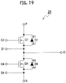
- Fig. 19 illustrates a schematic circuit representative of a 2-in-1 module, which is the power module 20 according to the embodiment.
- two MOSFETs Q1, Q4 are included in one module.
- Reference numeral G1 denotes a gate signal terminal of the MOSFET Q1
- reference numeral S1 denotes a source sense terminal of the MOSFET Q1.
- Reference numeral G4 denotes a gate signal terminal of the MOSFET Q4
- reference numeral S4 denotes a source sense terminal of the MOSFET Q4.
- Reference numeral P denotes a positive side power input terminal
- reference numeral N denotes a negative side power input terminal
- reference numeral O denotes an output terminal.
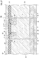
- a schematic cross-sectional structure of the SiC MOSFET as an example of the semiconductor device 100 (Q) applied to the power module 20 includes: a semiconductor substrate 26 composed of an n - type high resistivity layer; a p type base region 28 formed on the surface side of the semiconductor substrate 26; source regions 30 formed on the surface of the p type base regions 28; a gate insulating film 32 disposed on the surface of the semiconductor substrate 26 between the p type base regions 28; a gate electrode 38 disposed on the gate insulating film 32; a source electrode 34 connected to the source region 30 and the p type base region 28; an n + drain region 24 disposed on a back side surface opposite to the surface of the semiconductor substrate 26; and a drain pad electrode 36 connected to the n + drain region 24.
- the semiconductor device 100 is composed of a planar-gate-type n channel vertical SiC-MOSFET, the semiconductor device 100 may be composed of a trench-gate-type n channel vertical SiC-MOSFET, etc.
- GaN based FET etc. instead of SiC MOSFET are also applicable to the semiconductor device 100 (Q) applied to the power module 20 according to the embodiment.
- any one of an SiC based power device, a GaN based power device, and an AlN based power device is applicable to the semiconductor device 100 applied to the power module 20 according to the embodiment.
- a semiconductor of which the bandgap energy is from 1.1 eV to 8 eV, for example, can be used for the semiconductor device 100 applied to the power module 20 according to the embodiment.
- Fig. 21 illustrates a schematic cross-sectional structure of an SiC MOSFET including a source pad electrode SP and a gate pad electrode GP, which is an example of the semiconductor device 100 applied to the power module 20 according to the embodiment.
- the gate pad electrode GP is connected to the gate electrode 38 disposed on the gate insulating film 32, and the source pad electrode SP is connected to the source electrode 34 connected to the source region 30 and the p type base region 28.
- the gate pad electrode GP and the source pad electrode SP are disposed on an interlayer insulating film 44 for passivation which covers the surface of the semiconductor device 100.
- Microstructural transistor structure may be formed in the semiconductor substrate 26 below the gate pad electrode GP and the source pad electrode in the same manner as the center portion shown in Fig. 20 or 21 .
- the source pad electrode SP may be disposed to be extended onto the interlayer insulating film 44 for passivation, also in the transistor structure of the center portion.
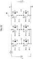
- Fig. 22 illustrates a circuit configuration to connect the snubber capacitor C between the power terminal PL and the earth terminal (ground terminal) NL.
- large surge voltage Ldi/dt is produced by an inductance L included in a connection line due to a high switching speed of the SiC device.
- the surge voltage Ldi/dt changes dependent on a value of the inductance L
- the surge voltage Ldi/dt is superimposed on the power source V.
- Such a surge voltage Ldi/dt can be absorbed by the snubber capacitor C connected between the power terminal PL and the earth terminal (ground terminal) NL.
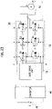
- the three-phase AC inverter 40 includes: a gate drive unit 50; a power module unit 52 connected to the gate drive unit 50 and a three-phase AC motor unit 54.
- U-phase, V-phase, and W-phase inverters are respectively connected to the three-phase AC motor unit 54 so as to correspond to U phase, V phase, and W phase of the three-phase AC motor unit 54, in the power module unit 52.
- the gate drive unit 50 is connected to the SiC MOSFETs Q1, Q4 as shown in Fig. 23
- the gate drive unit 50 is similarly connected also to the SiC MOSFETs Q2, Q5 and the SiC MOSFETs Q3, Q6 (not shown in Fig. 23 ).
- the SiC MOSFETs Q1, Q4, and Q2, Q5, and Q3, Q6 having inverter configurations are connected between a positive terminal (+) and a negative terminal (-) to which the converter 48 in a storage battery (E) 46 is connected. Furthermore, diodes D1-D6 are connected inversely in parallel to one another between the source and the drain of the SiC-MOSFETs Q1 to Q6.
- the three-phase power module unit 52 can also be formed also by similarly forming V phase and W phase inverters.
- the power module according to the embodiment can be formed as any one of 1-in-1, 2-in-1, 4-in-1, or 6-in-1 module.
- the power module with improved reliability so that the insulating layer and the metal layer may be hardly deviated from each other even if external force is applied thereon; and the fabrication method for such a power module.
- the insulating layer 7 is formed also between the leadframes 1 and 5 in Fig. 5 , the insulating layer 7 may not always be formed between the leadframes 1, 5, but may be formed only on a bottom surface of the leadframes 1, 5.
- the power module according to the present invention can be used for semiconductor modules, e.g. IGBT modules, diode modules, MOS modules (Si, SiC, GaN), etc.
- the power module according to the embodiment can also be used for structures which do not use insulating substrates, e.g. Direct Copper Bond (DBC) in case type modules.
- DBC Direct Copper Bond
Landscapes
- Cooling Or The Like Of Semiconductors Or Solid State Devices (AREA)
- Physics & Mathematics (AREA)
- Geometry (AREA)
- Chemical & Material Sciences (AREA)
- Engineering & Computer Science (AREA)
- Materials Engineering (AREA)
Claims (20)
- Leistungsmodul (20) mit:einer isolierenden Schicht (7), die eine Vorderfläche und eine Bodenfläche aufweist;einer Metallschicht (1), die auf der Vorderfläche der isolierenden Schicht (7) angeordnet ist;einem Halbleiterchip (3), der auf der Metallschicht (1) angeordnet ist; undeinem Gussharz (6), das so gebildet ist, dass es den Halbleiterchip (3) und wenigstens einen Teil der Metallschicht (1) und nur die Vorderflächenseite der isolierenden Schicht (7) bedeckt, wobeieine Vertiefung (11), in die hinein ein Teil der isolierenden Schicht (7) eingeführt ist, an einer Fläche der Metallschicht (1) gebildet ist, die hin zu der isolierenden Schicht (7) weist, und wobei die Bodenflächenseite der Isolierschicht (7) eine flache Fläche ist.
- Leistungsmodul nach Anspruch 1, wobei
eine Vielzahl der Vertiefungen (11) außerhalb einer dem Halbleiterchip (3) gegenüberliegenden Region der Metallschicht (1) gebildet sind. - Leistungsmodul nach Anspruch 2, wobei
die Region eine Region ist, bei der ein Winkel (C) zwischen einer Linie und einer flachen Fläche der Metallschicht (1) kleiner gleich 45 Grad ist, wobei die Linie eine Verbindung zwischen einem Randteil des Halbleiterchips (3) und einem Randteil jener Vertiefung (11) bildet, die von der Vielzahl der Vertiefungen dem Halbleiterchip (3) am nächsten ist. - Leistungsmodul nach Anspruch 2 oder 3, wobei
die Vielzahl der Vertiefungen (11) nur außerhalb einer dem Halbleiterchip (3) gegenüberliegenden Region der Metallschicht (1) gebildet sind. - Leistungsmodul nach einem beliebigen der Ansprüche 1 bis 4, wobei:eine Querschnittsform der Vertiefung (11) wenigstens eine Form ist, die ausgewählt ist aus der Gruppe, die aus einer rechteckigen Form, einer Halbkreisform, einer Halbellipsenform, einer Dreieckform und einer Keilform besteht; undwobei eine Tiefe der Vertiefung (11) etwa 0,5 bis 1,5 mm beträgt und wobei eine Dicke der Metallschicht (1) etwa 3,0 mm beträgt.
- Leistungsmodul nach einem beliebigen der Ansprüche 1 bis 5, wobei
die Vertiefung entlang einer Richtung gebildet ist oder in einer gitterartigen Form gebildet ist. - Leistungsmodul nach einem beliebigen der Ansprüche 1 bis 6, wobei
ein Oberflächen-Aufrauungsprozess auf eine hin zu der isolierenden Schicht (7) weisende Fläche der Metallschicht (5) angewendet wird. - Leistungsmodul nach einem beliebigen der Ansprüche 1 bis 7, wobei
die isolierende Schicht (7) aus einem weicheren Material als die Metallschicht (1) gebildet ist. - Leistungsmodul nach Anspruch 8, wobei
eine Härte der isolierenden Schicht (7) weicher bzw. niedriger ist als eine Durometerhärte A40. - Leistungsmodul nach einem beliebigen der Ansprüche 1 bis 9, wobei
die isolierende Schicht (7) aus einem organischen Material gebildet ist. - Leistungsmodul nach einem beliebigen der Ansprüche 1 bis 10, wobei
die isolierende Schicht (7) aus einem Silikon-basierten Harz gebildet ist. - Leistungsmodul nach einem beliebigen der Ansprüche 1 bis 11, wobei
die isolierende Schicht (7) mit einem thermisch hochleitenden Füllstoff aufgefüllt ist. - Leistungsmodul nach Anspruch 12, wobei
der Füllstoff wenigstens ein Füllstoff ist, der ausgewählt ist aus der Gruppe, die aus Aluminiumoxid, Siliziumoxid, Aluminiumnitrid, Siliciumnitrid, Bornitrid, Berylliumoxid und Magnesiumoxid besteht. - Leistungsmodul nach einem beliebigen der Ansprüche 1 bis 13, wobei
eine Oberfläche des Gussharzes (6) und eine Oberfläche der Metallschicht (1) an einem Eckabschnitt der Metallschicht bündig miteinander ausgerichtet sind und wobei die isolierende Schicht (7) auf der Oberfläche des Gussharzes (6) und der Oberfläche des Anschlussrahmens gebildet ist, die bündig miteinander ausgerichtet sind. - Leistungsmodul nach einem beliebigen der Ansprüche 2 bis 13, wobei
eine Distanz zwischen den benachbarten Vertiefungen und eine Breite von jeder Vertiefung etwa gleich groß sind. - Leistungsmodul nach Anspruch 15, wobeider Halbleiterchip (3) aus einem Bauteil gebildet ist, das ausgewählt ist aus der Gruppe, die aus einem SiC-basierten Leistungsbauteil, einem GaN-basierten Leistungsbauteil und einem AIN-basierten Leistungsbauteil besteht; undwobei eine Stromänderungsrate di/dt hiervon etwa 3×10⁹ (A/s) beträgt.
- Leistungsmodul nach Anspruch 1, wobei
die Vertiefung in einer Richtung einer kurzen Seite des Leistungsmoduls oder in einer Richtung einer langen Seite des Leistungsmoduls gebildet ist. - Leistungsmodul nach einem beliebigen der Ansprüche 1 bis 17, wobei
das Leistungsmodul (20) aus einem beliebigen Modul gebildet ist, das ausgewählt ist aus der Gruppe, die aus einem 1-in-1-Modul, einem 2-in-1-Modul, einem 4-in-1-Modul und einem 6-in-1-Modul besteht. - Herstellungsverfahren für ein Leistungsmodul (20), mit:Bilden einer Vertiefung (11) an einer Bodenfläche eines Anschlussrahmens (1);Bonden eines Halbleiterchips (3) an den Anschlussrahmen (1) mittels eines leitfähigen Bond-Materials (2);elektrisches Verbinden des Halbleiterchips (3) und des Anschlussrahmens (1) miteinander, und zwar unter Verwendung eines Verbindungselementes (4);Anordnen des Anschlussrahmens (1) an einer Metallgussform und Schließen der Metallgussform und anschließend Eingießen von einem Gussharz (6) hier hinein, um den Anschlussrahmen (1), das leitfähige Bond-Material (2), den Halbleiterchip (3) und das Verbindungselement (4) zu vergießen; undBilden einer isolierenden Schicht (7) auf einer Bodenfläche des Anschlussrahmens (1), wobei die isolierende Schicht (7) so gebildet ist, dass sie in die Bodenfläche des Anschlussrahmens (1) eingeführt wird, wobei die isolierende Schicht (7) eine Vorderfläche und eine Bodenfläche aufweist, wobei die Bodenflächenseite der isolierenden Schicht (7) als eine flache Fläche gebildet ist, so dass das Gussharz (6) nur die Vorderflächenseite der isolierenden Schicht (7) bedeckt.
- Herstellungsverfahren für ein Leistungsmodul nach Anspruch 19, wobei
bei dem Bilden der Vertiefung die Vertiefung (11) in einer Richtung einer kurzen Seite des Leistungsmoduls (20) oder in einer Richtung einer langen Seite des Leistungsmoduls (20) gebildet wird.
Applications Claiming Priority (2)
| Application Number | Priority Date | Filing Date | Title |
|---|---|---|---|
| JP2013151685A JP2015023211A (ja) | 2013-07-22 | 2013-07-22 | パワーモジュールおよびその製造方法 |
| PCT/JP2014/068978 WO2015012180A1 (ja) | 2013-07-22 | 2014-07-17 | パワーモジュールおよびその製造方法 |
Publications (3)
| Publication Number | Publication Date |
|---|---|
| EP3026701A1 EP3026701A1 (de) | 2016-06-01 |
| EP3026701A4 EP3026701A4 (de) | 2017-03-08 |
| EP3026701B1 true EP3026701B1 (de) | 2022-11-16 |
Family
ID=52393222
Family Applications (1)
| Application Number | Title | Priority Date | Filing Date |
|---|---|---|---|
| EP14829390.5A Active EP3026701B1 (de) | 2013-07-22 | 2014-07-17 | Leistungsmodul und herstellungsverfahren davon |
Country Status (4)
| Country | Link |
|---|---|
| US (1) | US9721875B2 (de) |
| EP (1) | EP3026701B1 (de) |
| JP (1) | JP2015023211A (de) |
| WO (1) | WO2015012180A1 (de) |
Families Citing this family (15)
| Publication number | Priority date | Publication date | Assignee | Title |
|---|---|---|---|---|
| JP6332439B2 (ja) * | 2014-03-31 | 2018-05-30 | 富士電機株式会社 | 電力変換装置 |
| JP6841199B2 (ja) * | 2017-09-29 | 2021-03-10 | 三菱電機株式会社 | 半導体装置 |
| DE112019001917T5 (de) | 2018-04-11 | 2020-12-24 | Rohm Co., Ltd. | Halbleiterbauteil |
| US11317546B2 (en) | 2018-06-26 | 2022-04-26 | Ford Global Technologies, Llc | Vehicle power module assembly |
| WO2020110287A1 (ja) | 2018-11-30 | 2020-06-04 | 日立金属株式会社 | 電気接続用部材、電気接続構造、および電気接続用部材の製造方法 |
| JP6818801B2 (ja) * | 2019-04-01 | 2021-01-20 | ローム株式会社 | パワーモジュールおよびその製造方法 |
| WO2020212031A1 (en) | 2019-04-18 | 2020-10-22 | Abb Power Grids Switzerland Ag | Power semiconductor module with laser-welded leadframe |
| CN110416178A (zh) * | 2019-07-12 | 2019-11-05 | 南通沃特光电科技有限公司 | 一种集成电路封装结构及其封装方法 |
| US11145578B2 (en) | 2019-09-24 | 2021-10-12 | Infineon Technologies Ag | Semiconductor package with top or bottom side cooling and method for manufacturing the semiconductor package |
| CN115380373B (zh) * | 2020-03-31 | 2023-08-01 | 日立能源瑞士股份公司 | 具有改进的热性能的功率模块装置 |
| JP6952834B1 (ja) * | 2020-06-04 | 2021-10-27 | 三菱電機株式会社 | パワーモジュール |
| EP4057338B1 (de) * | 2021-03-10 | 2026-05-06 | Hitachi Energy Ltd | Metallsubstratstruktur und verfahren zur herstellung einer metallsubstratstruktur für ein halbleiterleistungsmodul sowie halbleiterleistungsmodul |
| JP7653882B2 (ja) | 2021-09-22 | 2025-03-31 | 株式会社東芝 | 半導体装置 |
| DE112022007496T5 (de) * | 2022-07-07 | 2025-04-17 | Mitsubishi Electric Corporation | Halbleitervorrichtung und leistungsumwandlungsvorrichtung |
| WO2025262832A1 (ja) * | 2024-06-19 | 2025-12-26 | 株式会社オートネットワーク技術研究所 | ヒートシンク付回路基板およびその製造方法 |
Citations (1)
| Publication number | Priority date | Publication date | Assignee | Title |
|---|---|---|---|---|
| JP2001118961A (ja) * | 1999-10-15 | 2001-04-27 | Mitsubishi Electric Corp | 樹脂封止型電力用半導体装置及びその製造方法 |
Family Cites Families (17)
| Publication number | Priority date | Publication date | Assignee | Title |
|---|---|---|---|---|
| JP3201277B2 (ja) | 1996-09-11 | 2001-08-20 | 株式会社日立製作所 | 半導体装置 |
| JPH10125826A (ja) * | 1996-10-24 | 1998-05-15 | Hitachi Ltd | 半導体装置及びその製法 |
| JP3605547B2 (ja) * | 1999-06-11 | 2004-12-22 | 松下電器産業株式会社 | 放熱基板及びその製造方法 |
| JP2002167560A (ja) * | 2000-12-01 | 2002-06-11 | Sekisui Chem Co Ltd | 熱伝導性樹脂シート |
| JP2005109100A (ja) | 2003-09-30 | 2005-04-21 | Mitsubishi Electric Corp | 半導体装置およびその製造方法 |
| JP5186095B2 (ja) * | 2006-10-02 | 2013-04-17 | 株式会社日立製作所 | ゲート駆動回路 |
| JP2008153430A (ja) * | 2006-12-18 | 2008-07-03 | Mitsubishi Electric Corp | 放熱基板並びに熱伝導性シートおよびこれらを用いたパワーモジュール |
| JP2008300379A (ja) * | 2007-05-29 | 2008-12-11 | Sumitomo Electric Ind Ltd | パワーモジュール |
| JP5262983B2 (ja) * | 2009-05-19 | 2013-08-14 | 株式会社デンソー | モールドパッケージおよびその製造方法 |
| JP2011100757A (ja) * | 2009-11-04 | 2011-05-19 | Denki Kagaku Kogyo Kk | 電子部品及びその製造方法 |
| JP5246143B2 (ja) * | 2009-11-24 | 2013-07-24 | 富士電機株式会社 | 半導体モジュールおよびその製造方法ならびに電気機器 |
| KR101410553B1 (ko) * | 2010-07-01 | 2014-06-20 | 미쓰비시덴키 가부시키가이샤 | 파워 반도체 모듈, 전력 변환 장치, 및 철도 차량 |
| JP5409551B2 (ja) * | 2010-08-24 | 2014-02-05 | 新電元工業株式会社 | 半導体装置 |
| JP5251991B2 (ja) * | 2011-01-14 | 2013-07-31 | トヨタ自動車株式会社 | 半導体モジュール |
| JP5249365B2 (ja) * | 2011-01-26 | 2013-07-31 | 三菱電機株式会社 | 電力変換装置 |
| JP5690752B2 (ja) * | 2012-01-10 | 2015-03-25 | 日立オートモティブシステムズ株式会社 | パワー半導体モジュールおよびパワー半導体モジュールの製造方法 |
| JP2013258387A (ja) * | 2012-05-15 | 2013-12-26 | Rohm Co Ltd | パワーモジュール半導体装置 |
-
2013
- 2013-07-22 JP JP2013151685A patent/JP2015023211A/ja active Pending
-
2014
- 2014-07-17 WO PCT/JP2014/068978 patent/WO2015012180A1/ja not_active Ceased
- 2014-07-17 EP EP14829390.5A patent/EP3026701B1/de active Active
-
2016
- 2016-01-21 US US15/003,156 patent/US9721875B2/en active Active
Patent Citations (1)
| Publication number | Priority date | Publication date | Assignee | Title |
|---|---|---|---|---|
| JP2001118961A (ja) * | 1999-10-15 | 2001-04-27 | Mitsubishi Electric Corp | 樹脂封止型電力用半導体装置及びその製造方法 |
Also Published As
| Publication number | Publication date |
|---|---|
| JP2015023211A (ja) | 2015-02-02 |
| US9721875B2 (en) | 2017-08-01 |
| US20160141231A1 (en) | 2016-05-19 |
| WO2015012180A1 (ja) | 2015-01-29 |
| EP3026701A4 (de) | 2017-03-08 |
| EP3026701A1 (de) | 2016-06-01 |
Similar Documents
| Publication | Publication Date | Title |
|---|---|---|
| EP3026701B1 (de) | Leistungsmodul und herstellungsverfahren davon | |
| JP6280265B2 (ja) | パワーモジュール半導体装置 | |
| US10778113B2 (en) | Intelligent power module, electric vehicle, and hybrid car | |
| JP6077773B2 (ja) | パワーモジュール半導体装置 | |
| JP5067267B2 (ja) | 樹脂封止型半導体装置とその製造方法 | |
| CN102820271B (zh) | 半导体装置 | |
| EP3026700B1 (de) | Leistungsmodul und herstellungsverfahren davon | |
| US20180350710A1 (en) | Semiconductor device, and power module | |
| US20150130042A1 (en) | Semiconductor module with radiation fins | |
| US9437508B2 (en) | Method for manufacturing semiconductor device and semiconductor device | |
| JP6575739B1 (ja) | 半導体装置、半導体装置の製造方法および電力変換装置 | |
| KR20150058015A (ko) | 반도체 장치 및 반도체 장치의 제조 방법 | |
| JP6818801B2 (ja) | パワーモジュールおよびその製造方法 | |
| JP2012248700A (ja) | 半導体装置 | |
| CN113261095B (zh) | 半导体装置、半导体装置的制造方法及电力转换装置 | |
| JP7019024B2 (ja) | 半導体装置及び電力変換装置 | |
| JPWO2018181417A1 (ja) | パワーモジュールおよびその製造方法 | |
| WO2018047485A1 (ja) | パワーモジュールおよびインバータ装置 | |
| JP7512659B2 (ja) | 半導体モジュール及び半導体モジュールの製造方法 | |
| JP2018088558A (ja) | 半導体装置 | |
| JP2019040955A (ja) | 半導体モジュールの製造方法 | |
| WO2025182086A1 (ja) | 電力用半導体装置および電力変換装置 | |
| JP2025115059A (ja) | 半導体モジュール |
Legal Events
| Date | Code | Title | Description |
|---|---|---|---|
| PUAI | Public reference made under article 153(3) epc to a published international application that has entered the european phase |
Free format text: ORIGINAL CODE: 0009012 |
|
| 17P | Request for examination filed |
Effective date: 20160222 |
|
| AK | Designated contracting states |
Kind code of ref document: A1 Designated state(s): AL AT BE BG CH CY CZ DE DK EE ES FI FR GB GR HR HU IE IS IT LI LT LU LV MC MK MT NL NO PL PT RO RS SE SI SK SM TR |
|
| AX | Request for extension of the european patent |
Extension state: BA ME |
|
| DAX | Request for extension of the european patent (deleted) | ||
| A4 | Supplementary search report drawn up and despatched |
Effective date: 20170202 |
|
| RIC1 | Information provided on ipc code assigned before grant |
Ipc: H01L 23/495 20060101AFI20170127BHEP Ipc: H01L 23/34 20060101ALI20170127BHEP |
|
| STAA | Information on the status of an ep patent application or granted ep patent |
Free format text: STATUS: EXAMINATION IS IN PROGRESS |
|
| 17Q | First examination report despatched |
Effective date: 20210429 |
|
| REG | Reference to a national code |
Ref country code: DE Ref legal event code: R079 Ref document number: 602014085567 Country of ref document: DE Free format text: PREVIOUS MAIN CLASS: H01L0023340000 Ipc: H01L0023495000 |
|
| GRAP | Despatch of communication of intention to grant a patent |
Free format text: ORIGINAL CODE: EPIDOSNIGR1 |
|
| STAA | Information on the status of an ep patent application or granted ep patent |
Free format text: STATUS: GRANT OF PATENT IS INTENDED |
|
| RIC1 | Information provided on ipc code assigned before grant |
Ipc: H01L 23/31 20060101ALI20220428BHEP Ipc: H01L 23/34 20060101ALI20220428BHEP Ipc: H01L 23/495 20060101AFI20220428BHEP |
|
| INTG | Intention to grant announced |
Effective date: 20220601 |
|
| GRAS | Grant fee paid |
Free format text: ORIGINAL CODE: EPIDOSNIGR3 |
|
| GRAA | (expected) grant |
Free format text: ORIGINAL CODE: 0009210 |
|
| STAA | Information on the status of an ep patent application or granted ep patent |
Free format text: STATUS: THE PATENT HAS BEEN GRANTED |
|
| AK | Designated contracting states |
Kind code of ref document: B1 Designated state(s): AL AT BE BG CH CY CZ DE DK EE ES FI FR GB GR HR HU IE IS IT LI LT LU LV MC MK MT NL NO PL PT RO RS SE SI SK SM TR |
|
| REG | Reference to a national code |
Ref country code: GB Ref legal event code: FG4D |
|
| REG | Reference to a national code |
Ref country code: CH Ref legal event code: EP |
|
| REG | Reference to a national code |
Ref country code: DE Ref legal event code: R096 Ref document number: 602014085567 Country of ref document: DE |
|
| REG | Reference to a national code |
Ref country code: IE Ref legal event code: FG4D |
|
| REG | Reference to a national code |
Ref country code: AT Ref legal event code: REF Ref document number: 1532291 Country of ref document: AT Kind code of ref document: T Effective date: 20221215 |
|
| REG | Reference to a national code |
Ref country code: LT Ref legal event code: MG9D |
|
| REG | Reference to a national code |
Ref country code: NL Ref legal event code: MP Effective date: 20221116 |
|
| REG | Reference to a national code |
Ref country code: AT Ref legal event code: MK05 Ref document number: 1532291 Country of ref document: AT Kind code of ref document: T Effective date: 20221116 |
|
| PG25 | Lapsed in a contracting state [announced via postgrant information from national office to epo] |
Ref country code: SE Free format text: LAPSE BECAUSE OF FAILURE TO SUBMIT A TRANSLATION OF THE DESCRIPTION OR TO PAY THE FEE WITHIN THE PRESCRIBED TIME-LIMIT Effective date: 20221116 Ref country code: PT Free format text: LAPSE BECAUSE OF FAILURE TO SUBMIT A TRANSLATION OF THE DESCRIPTION OR TO PAY THE FEE WITHIN THE PRESCRIBED TIME-LIMIT Effective date: 20230316 Ref country code: NO Free format text: LAPSE BECAUSE OF FAILURE TO SUBMIT A TRANSLATION OF THE DESCRIPTION OR TO PAY THE FEE WITHIN THE PRESCRIBED TIME-LIMIT Effective date: 20230216 Ref country code: LT Free format text: LAPSE BECAUSE OF FAILURE TO SUBMIT A TRANSLATION OF THE DESCRIPTION OR TO PAY THE FEE WITHIN THE PRESCRIBED TIME-LIMIT Effective date: 20221116 Ref country code: FI Free format text: LAPSE BECAUSE OF FAILURE TO SUBMIT A TRANSLATION OF THE DESCRIPTION OR TO PAY THE FEE WITHIN THE PRESCRIBED TIME-LIMIT Effective date: 20221116 Ref country code: ES Free format text: LAPSE BECAUSE OF FAILURE TO SUBMIT A TRANSLATION OF THE DESCRIPTION OR TO PAY THE FEE WITHIN THE PRESCRIBED TIME-LIMIT Effective date: 20221116 Ref country code: AT Free format text: LAPSE BECAUSE OF FAILURE TO SUBMIT A TRANSLATION OF THE DESCRIPTION OR TO PAY THE FEE WITHIN THE PRESCRIBED TIME-LIMIT Effective date: 20221116 |
|
| PG25 | Lapsed in a contracting state [announced via postgrant information from national office to epo] |
Ref country code: RS Free format text: LAPSE BECAUSE OF FAILURE TO SUBMIT A TRANSLATION OF THE DESCRIPTION OR TO PAY THE FEE WITHIN THE PRESCRIBED TIME-LIMIT Effective date: 20221116 Ref country code: PL Free format text: LAPSE BECAUSE OF FAILURE TO SUBMIT A TRANSLATION OF THE DESCRIPTION OR TO PAY THE FEE WITHIN THE PRESCRIBED TIME-LIMIT Effective date: 20221116 Ref country code: LV Free format text: LAPSE BECAUSE OF FAILURE TO SUBMIT A TRANSLATION OF THE DESCRIPTION OR TO PAY THE FEE WITHIN THE PRESCRIBED TIME-LIMIT Effective date: 20221116 Ref country code: IS Free format text: LAPSE BECAUSE OF FAILURE TO SUBMIT A TRANSLATION OF THE DESCRIPTION OR TO PAY THE FEE WITHIN THE PRESCRIBED TIME-LIMIT Effective date: 20230316 Ref country code: HR Free format text: LAPSE BECAUSE OF FAILURE TO SUBMIT A TRANSLATION OF THE DESCRIPTION OR TO PAY THE FEE WITHIN THE PRESCRIBED TIME-LIMIT Effective date: 20221116 Ref country code: GR Free format text: LAPSE BECAUSE OF FAILURE TO SUBMIT A TRANSLATION OF THE DESCRIPTION OR TO PAY THE FEE WITHIN THE PRESCRIBED TIME-LIMIT Effective date: 20230217 |
|
| P01 | Opt-out of the competence of the unified patent court (upc) registered |
Effective date: 20230421 |
|
| PG25 | Lapsed in a contracting state [announced via postgrant information from national office to epo] |
Ref country code: NL Free format text: LAPSE BECAUSE OF FAILURE TO SUBMIT A TRANSLATION OF THE DESCRIPTION OR TO PAY THE FEE WITHIN THE PRESCRIBED TIME-LIMIT Effective date: 20221116 |
|
| PG25 | Lapsed in a contracting state [announced via postgrant information from national office to epo] |
Ref country code: SM Free format text: LAPSE BECAUSE OF FAILURE TO SUBMIT A TRANSLATION OF THE DESCRIPTION OR TO PAY THE FEE WITHIN THE PRESCRIBED TIME-LIMIT Effective date: 20221116 Ref country code: RO Free format text: LAPSE BECAUSE OF FAILURE TO SUBMIT A TRANSLATION OF THE DESCRIPTION OR TO PAY THE FEE WITHIN THE PRESCRIBED TIME-LIMIT Effective date: 20221116 Ref country code: EE Free format text: LAPSE BECAUSE OF FAILURE TO SUBMIT A TRANSLATION OF THE DESCRIPTION OR TO PAY THE FEE WITHIN THE PRESCRIBED TIME-LIMIT Effective date: 20221116 Ref country code: DK Free format text: LAPSE BECAUSE OF FAILURE TO SUBMIT A TRANSLATION OF THE DESCRIPTION OR TO PAY THE FEE WITHIN THE PRESCRIBED TIME-LIMIT Effective date: 20221116 Ref country code: CZ Free format text: LAPSE BECAUSE OF FAILURE TO SUBMIT A TRANSLATION OF THE DESCRIPTION OR TO PAY THE FEE WITHIN THE PRESCRIBED TIME-LIMIT Effective date: 20221116 |
|
| REG | Reference to a national code |
Ref country code: DE Ref legal event code: R097 Ref document number: 602014085567 Country of ref document: DE |
|
| PG25 | Lapsed in a contracting state [announced via postgrant information from national office to epo] |
Ref country code: SK Free format text: LAPSE BECAUSE OF FAILURE TO SUBMIT A TRANSLATION OF THE DESCRIPTION OR TO PAY THE FEE WITHIN THE PRESCRIBED TIME-LIMIT Effective date: 20221116 Ref country code: AL Free format text: LAPSE BECAUSE OF FAILURE TO SUBMIT A TRANSLATION OF THE DESCRIPTION OR TO PAY THE FEE WITHIN THE PRESCRIBED TIME-LIMIT Effective date: 20221116 |
|
| PLBE | No opposition filed within time limit |
Free format text: ORIGINAL CODE: 0009261 |
|
| STAA | Information on the status of an ep patent application or granted ep patent |
Free format text: STATUS: NO OPPOSITION FILED WITHIN TIME LIMIT |
|
| 26N | No opposition filed |
Effective date: 20230817 |
|
| PG25 | Lapsed in a contracting state [announced via postgrant information from national office to epo] |
Ref country code: SI Free format text: LAPSE BECAUSE OF FAILURE TO SUBMIT A TRANSLATION OF THE DESCRIPTION OR TO PAY THE FEE WITHIN THE PRESCRIBED TIME-LIMIT Effective date: 20221116 |
|
| PG25 | Lapsed in a contracting state [announced via postgrant information from national office to epo] |
Ref country code: MC Free format text: LAPSE BECAUSE OF FAILURE TO SUBMIT A TRANSLATION OF THE DESCRIPTION OR TO PAY THE FEE WITHIN THE PRESCRIBED TIME-LIMIT Effective date: 20221116 |
|
| PG25 | Lapsed in a contracting state [announced via postgrant information from national office to epo] |
Ref country code: MC Free format text: LAPSE BECAUSE OF FAILURE TO SUBMIT A TRANSLATION OF THE DESCRIPTION OR TO PAY THE FEE WITHIN THE PRESCRIBED TIME-LIMIT Effective date: 20221116 |
|
| REG | Reference to a national code |
Ref country code: CH Ref legal event code: PL |
|
| REG | Reference to a national code |
Ref country code: BE Ref legal event code: MM Effective date: 20230731 |
|
| PG25 | Lapsed in a contracting state [announced via postgrant information from national office to epo] |
Ref country code: LU Free format text: LAPSE BECAUSE OF NON-PAYMENT OF DUE FEES Effective date: 20230717 |
|
| GBPC | Gb: european patent ceased through non-payment of renewal fee |
Effective date: 20230717 |
|
| PG25 | Lapsed in a contracting state [announced via postgrant information from national office to epo] |
Ref country code: LU Free format text: LAPSE BECAUSE OF NON-PAYMENT OF DUE FEES Effective date: 20230717 |
|
| REG | Reference to a national code |
Ref country code: IE Ref legal event code: MM4A |
|
| PG25 | Lapsed in a contracting state [announced via postgrant information from national office to epo] |
Ref country code: GB Free format text: LAPSE BECAUSE OF NON-PAYMENT OF DUE FEES Effective date: 20230717 Ref country code: CH Free format text: LAPSE BECAUSE OF NON-PAYMENT OF DUE FEES Effective date: 20230731 |
|
| PG25 | Lapsed in a contracting state [announced via postgrant information from national office to epo] |
Ref country code: IT Free format text: LAPSE BECAUSE OF FAILURE TO SUBMIT A TRANSLATION OF THE DESCRIPTION OR TO PAY THE FEE WITHIN THE PRESCRIBED TIME-LIMIT Effective date: 20221116 Ref country code: FR Free format text: LAPSE BECAUSE OF NON-PAYMENT OF DUE FEES Effective date: 20230731 Ref country code: BE Free format text: LAPSE BECAUSE OF NON-PAYMENT OF DUE FEES Effective date: 20230731 |
|
| PG25 | Lapsed in a contracting state [announced via postgrant information from national office to epo] |
Ref country code: IE Free format text: LAPSE BECAUSE OF NON-PAYMENT OF DUE FEES Effective date: 20230717 |
|
| PG25 | Lapsed in a contracting state [announced via postgrant information from national office to epo] |
Ref country code: IE Free format text: LAPSE BECAUSE OF NON-PAYMENT OF DUE FEES Effective date: 20230717 |
|
| PG25 | Lapsed in a contracting state [announced via postgrant information from national office to epo] |
Ref country code: BG Free format text: LAPSE BECAUSE OF FAILURE TO SUBMIT A TRANSLATION OF THE DESCRIPTION OR TO PAY THE FEE WITHIN THE PRESCRIBED TIME-LIMIT Effective date: 20221116 |
|
| PG25 | Lapsed in a contracting state [announced via postgrant information from national office to epo] |
Ref country code: BG Free format text: LAPSE BECAUSE OF FAILURE TO SUBMIT A TRANSLATION OF THE DESCRIPTION OR TO PAY THE FEE WITHIN THE PRESCRIBED TIME-LIMIT Effective date: 20221116 |
|
| PG25 | Lapsed in a contracting state [announced via postgrant information from national office to epo] |
Ref country code: CY Free format text: LAPSE BECAUSE OF FAILURE TO SUBMIT A TRANSLATION OF THE DESCRIPTION OR TO PAY THE FEE WITHIN THE PRESCRIBED TIME-LIMIT; INVALID AB INITIO Effective date: 20140717 |
|
| PG25 | Lapsed in a contracting state [announced via postgrant information from national office to epo] |
Ref country code: HU Free format text: LAPSE BECAUSE OF FAILURE TO SUBMIT A TRANSLATION OF THE DESCRIPTION OR TO PAY THE FEE WITHIN THE PRESCRIBED TIME-LIMIT; INVALID AB INITIO Effective date: 20140717 |
|
| PGFP | Annual fee paid to national office [announced via postgrant information from national office to epo] |
Ref country code: DE Payment date: 20250528 Year of fee payment: 12 |
|
| REG | Reference to a national code |
Ref country code: DE Ref legal event code: R079 Ref document number: 602014085567 Country of ref document: DE Free format text: PREVIOUS MAIN CLASS: H01L0023495000 Ipc: H10W0070400000 |
|
| PG25 | Lapsed in a contracting state [announced via postgrant information from national office to epo] |
Ref country code: TR Free format text: LAPSE BECAUSE OF FAILURE TO SUBMIT A TRANSLATION OF THE DESCRIPTION OR TO PAY THE FEE WITHIN THE PRESCRIBED TIME-LIMIT Effective date: 20221116 |