EP3029710A1 - Ladungsträgerstrahlvorrichtung und bilderfassungsverfahren - Google Patents
Ladungsträgerstrahlvorrichtung und bilderfassungsverfahren Download PDFInfo
- Publication number
- EP3029710A1 EP3029710A1 EP15197337.7A EP15197337A EP3029710A1 EP 3029710 A1 EP3029710 A1 EP 3029710A1 EP 15197337 A EP15197337 A EP 15197337A EP 3029710 A1 EP3029710 A1 EP 3029710A1
- Authority
- EP
- European Patent Office
- Prior art keywords
- frame image
- scanning
- phase
- corresponds
- image
- Prior art date
- Legal status (The legal status is an assumption and is not a legal conclusion. Google has not performed a legal analysis and makes no representation as to the accuracy of the status listed.)
- Withdrawn
Links
- 239000002245 particle Substances 0.000 title claims abstract description 79
- 238000000034 method Methods 0.000 title claims description 47
- 238000006073 displacement reaction Methods 0.000 claims abstract description 93
- 230000010363 phase shift Effects 0.000 claims abstract description 26
- 230000007274 generation of a signal involved in cell-cell signaling Effects 0.000 claims abstract description 17
- 238000001514 detection method Methods 0.000 claims description 26
- 238000010894 electron beam technology Methods 0.000 description 51
- 230000001360 synchronised effect Effects 0.000 description 21
- 230000004048 modification Effects 0.000 description 15
- 238000012986 modification Methods 0.000 description 15
- 125000004122 cyclic group Chemical group 0.000 description 14
- 239000000284 extract Substances 0.000 description 7
- 238000001878 scanning electron micrograph Methods 0.000 description 7
- 238000005259 measurement Methods 0.000 description 6
- 230000006870 function Effects 0.000 description 5
- 230000008602 contraction Effects 0.000 description 4
- 230000014509 gene expression Effects 0.000 description 4
- 230000000694 effects Effects 0.000 description 3
- 230000001788 irregular Effects 0.000 description 2
- 230000003287 optical effect Effects 0.000 description 2
- 239000004065 semiconductor Substances 0.000 description 2
- 238000009429 electrical wiring Methods 0.000 description 1
- 238000009434 installation Methods 0.000 description 1
- 239000000463 material Substances 0.000 description 1
- 239000000523 sample Substances 0.000 description 1
- WFKWXMTUELFFGS-UHFFFAOYSA-N tungsten Chemical compound [W] WFKWXMTUELFFGS-UHFFFAOYSA-N 0.000 description 1
- 229910052721 tungsten Inorganic materials 0.000 description 1
- 239000010937 tungsten Substances 0.000 description 1
Images







Classifications
-
- H—ELECTRICITY
- H01—ELECTRIC ELEMENTS
- H01J—ELECTRIC DISCHARGE TUBES OR DISCHARGE LAMPS
- H01J37/00—Discharge tubes with provision for introducing objects or material to be exposed to the discharge, e.g. for the purpose of examination or processing thereof
- H01J37/02—Details
- H01J37/04—Arrangements of electrodes and associated parts for generating or controlling the discharge, e.g. electron-optical arrangement or ion-optical arrangement
- H01J37/147—Arrangements for directing or deflecting the discharge along a desired path
-
- H—ELECTRICITY
- H01—ELECTRIC ELEMENTS
- H01J—ELECTRIC DISCHARGE TUBES OR DISCHARGE LAMPS
- H01J37/00—Discharge tubes with provision for introducing objects or material to be exposed to the discharge, e.g. for the purpose of examination or processing thereof
- H01J37/02—Details
- H01J37/04—Arrangements of electrodes and associated parts for generating or controlling the discharge, e.g. electron-optical arrangement or ion-optical arrangement
- H01J37/147—Arrangements for directing or deflecting the discharge along a desired path
- H01J37/1472—Deflecting along given lines
- H01J37/1474—Scanning means
-
- H—ELECTRICITY
- H01—ELECTRIC ELEMENTS
- H01J—ELECTRIC DISCHARGE TUBES OR DISCHARGE LAMPS
- H01J37/00—Discharge tubes with provision for introducing objects or material to be exposed to the discharge, e.g. for the purpose of examination or processing thereof
- H01J37/02—Details
- H01J37/244—Detectors; Associated components or circuits therefor
-
- H—ELECTRICITY
- H01—ELECTRIC ELEMENTS
- H01J—ELECTRIC DISCHARGE TUBES OR DISCHARGE LAMPS
- H01J37/00—Discharge tubes with provision for introducing objects or material to be exposed to the discharge, e.g. for the purpose of examination or processing thereof
- H01J37/26—Electron or ion microscopes; Electron or ion diffraction tubes
- H01J37/28—Electron or ion microscopes; Electron or ion diffraction tubes with scanning beams
-
- H—ELECTRICITY
- H01—ELECTRIC ELEMENTS
- H01J—ELECTRIC DISCHARGE TUBES OR DISCHARGE LAMPS
- H01J2237/00—Discharge tubes exposing object to beam, e.g. for analysis treatment, etching, imaging
- H01J2237/02—Details
- H01J2237/0216—Means for avoiding or correcting vibration effects
-
- H—ELECTRICITY
- H01—ELECTRIC ELEMENTS
- H01J—ELECTRIC DISCHARGE TUBES OR DISCHARGE LAMPS
- H01J2237/00—Discharge tubes exposing object to beam, e.g. for analysis treatment, etching, imaging
- H01J2237/15—Means for deflecting or directing discharge
-
- H—ELECTRICITY
- H01—ELECTRIC ELEMENTS
- H01J—ELECTRIC DISCHARGE TUBES OR DISCHARGE LAMPS
- H01J2237/00—Discharge tubes exposing object to beam, e.g. for analysis treatment, etching, imaging
- H01J2237/153—Correcting image defects, e.g. stigmators
- H01J2237/1536—Image distortions due to scanning
-
- H—ELECTRICITY
- H01—ELECTRIC ELEMENTS
- H01J—ELECTRIC DISCHARGE TUBES OR DISCHARGE LAMPS
- H01J2237/00—Discharge tubes exposing object to beam, e.g. for analysis treatment, etching, imaging
- H01J2237/22—Treatment of data
- H01J2237/221—Image processing
-
- H—ELECTRICITY
- H01—ELECTRIC ELEMENTS
- H01J—ELECTRIC DISCHARGE TUBES OR DISCHARGE LAMPS
- H01J2237/00—Discharge tubes exposing object to beam, e.g. for analysis treatment, etching, imaging
- H01J2237/26—Electron or ion microscopes
- H01J2237/28—Scanning microscopes
- H01J2237/2801—Details
Definitions
- the present invention relates to a charged particle beam device and an image acquisition method.
- a charged particle beam device e.g., a scanning electron microscope that is used to observe and analyze the microscopic structure of a living organism, a material, a semiconductor, or the like, and a critical dimension scanning electron microscope that is used to measure the dimensions of a semiconductor device circuit pattern
- a scanning electron microscope that is used to observe and analyze the microscopic structure of a living organism, a material, a semiconductor, or the like, and a critical dimension scanning electron microscope that is used to measure the dimensions of a semiconductor device circuit pattern
- a scanning electron microscope two-dimensionally scans an electron beam emitted from an electron source over a specimen (target) while narrowing down the electron beam, and detects secondary electrons, backscattered electrons, and the like generated from the specimen upon application of the electron beam to generate an image.
- the optical column of such a scanning electron microscope is normally exposed to an external disturbance magnetic field that occurs due to the installation environment.
- the main component of the external disturbance magnetic field include an alternating-current magnetic field that occurs due to electrical wiring provided in a room in which the device is installed.
- the electron beam is deflected by the alternating-current magnetic field, and has a cyclically distorted shape (see FIG. 14 ) instead of the original linear shape.
- FIG. 14 represents a scanning line
- each number illustrated in FIG. 14 is a number assigned to each scanning line.
- JP-A-2007-149348 discloses an electron microscope that is configured to reduce the effects of a magnetic field due to an AC power supply by synchronizing the two-dimensional scanning timing with the frequency phase of the AC power supply.
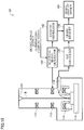
- FIG. 15 is a view schematically illustrating the configuration of an electron microscope 101 that is an example of an existing charged particle beam device.
- the electron microscope 101 includes an electron source 111, a condenser lens 112, a scanning deflector 113, an objective lens 114, a specimen stage 115, a detector 116, a scanning signal generator 120, an A/D converter 130, a frame memory 140, an address generator 142, and an image display device 150.
- the electron microscope 101 is configured so that an electron beam B generated by the electron source 111 is narrowed down by the condenser lens 112 and the objective lens 114, deflected by the scanning deflector 113, and scanned over the surface of a specimen S that is supported by the specimen stage 115. Secondary electrons and the like generated by the specimen S are detected by the detector 116, and converted into an electrical signal. The electrical signal is converted into a digital signal by the A/D converter 130, stored in a memory pixel that is included in the frame memory 140 and has an address designated by the address generator 142 corresponding to the scanning signal, and displayed on the image display device 150.
- the scanning signal generator 120 generates the scanning signal that has a sawtooth-like waveform, and drives the scanning deflector 113.
- the timing at which an image is stored in the frame memory 140 is synchronized with the scanning signal generated by the scanning signal generator 120.
- the scanning signal generator 120 raster-scans the electron beam so as to draw each scanning line in synchronization with a device power supply alternating-current signal.
- FIG. 16 is a view illustrating raster scanning that is synchronized with a power supply.
- the scanning of the electron beam that draws each scanning line is started from the same phase of the device power supply alternating-current signal. Therefore, the distortion of each scanning line due to the external disturbance magnetic field starts at the left end of the frame (see FIG. 16 ). Therefore, an image that does not undergo expansion and contraction in an irregular direction is obtained.
- Several aspects of the invention may provide a charged particle beam device and an image acquisition method that make it possible to reduce cyclic distortion of an image caused by an external disturbance magnetic field.
- a charged particle beam device that scans a charged particle beam in synchronization with an alternating-current signal, the charged particle beam device including:
- a charged particle beam device that scans a charged particle beam in synchronization with an alternating-current signal
- the charged particle beam device including: an image displacement vector calculation section that calculates an image displacement vector between a first local frame image and a second local frame image, the first local frame image including an area in a first frame image that is obtained by starting scanning at a timing that corresponds to a first phase of the alternating-current signal, and the area corresponds to a phase that undergoes a given phase shift from the first phase; the second local frame image including an area in a second frame image that is obtained by starting scanning at a timing that corresponds to a second phase of the alternating-current signal that differs from the first phase, and the area in the second frame image corresponds to a phase that undergoes the given phase shift from the second phase; a frame memory that includes a plurality of memory pixels; an address correction signal generation section that generates an address correction signal that corrects an address of a memory pixel among the plurality of memory
- an image acquisition method that is implemented in a charged particle beam device that scans a charged particle beam in synchronization with an alternating-current signal, the image acquisition method including:
- an image acquisition method that is implemented in a charged particle beam device that scans a charged particle beam in synchronization with an alternating-current signal, the image acquisition method including:
- the charged particle beam devices according to the embodiments of the invention are described below taking a scanning electron microscope (SEM) as an example. Note that the charged particle beam devices according to the embodiments of the invention may also be applied to a charged particle beam device, critical dimension scanning electron microscope for example, other than a scanning electron microscope.
- SEM scanning electron microscope
- FIG. 1 is a view schematically illustrating the configuration of an electron microscope 100 according to the first embodiment.
- the electron microscope 100 includes an electron source 11 (i.e., charged particle source), a condenser lens 12, a scanning deflector 13, an objective lens 14, a specimen stage 15, a detector 16, a scanning signal generator 20 (i.e., scanning signal supply section), an A/D converter 30, a frame memory 40, an address generator 42 (i.e., address selection section), an image display device 50, an image displacement vector calculator 60 (i.e., image displacement vector calculation section), and a scanning correction signal generator 70 (i.e., scanning correction signal generation section).
- the electron microscope 100 also includes various lenses, an aperture, and the like (not illustrated).
- the electron microscope 100 may have a configuration in which some of the elements illustrated in FIG. 1 are omitted or changed, or may have a configuration in which an additional element is further provided.
- the electron source 11 is a known electron gun, for example.
- the electron source 11 accelerates electrons released from a cathode using an anode to emit an electron beam B.
- An arbitrary electron gun may be used as the electron source 11.
- a tungsten filament thermionic-emission electron gun, a thermal field-emission electron gun, a cold cathode field-emission electron gun, or the like may be used as the electron source 11.
- the condenser lens 12 focuses the electron beam B emitted from the electron source 11.
- the scanning deflector 13 scans the electron beam B over a specimen S while deflecting the electron beam B.
- the scanning deflector 13 includes an electromagnetic coil, and deflects the electron beam B using a magnetic field, for example.
- the scanning deflector 13 can two-dimensionally scan the electron beam B while deflecting the electron beam B.
- the scanning deflector 13 scans the electron beam B based on an output signal (i.e., a scanning signal to which a scanning correction signal is added (described later)) from the scanning signal generator 20.
- the objective lens 14 focuses the electron beam B.
- the electron microscope 100 scans the electron beam B (electron probe) focused by the condenser lens 12 and the objective lens 14 over the specimen S using the scanning deflector 13.
- the specimen stage 15 supports the specimen S, and allows for example vertical and horizontal movement, rotation and tilting in the specimen S.
- the detector 16 detects a signal that is secondary electrons or backscattered electrons obtained by applying the focused electron beam B to the specimen S.
- the detection signal, that is secondary electron or backscattered electron detection signal detected by the detector 16 is converted into a digital signal by the A/D converter 30, and stored in the frame memory 40.
- the scanning signal generator 20 generates the scanning signal for scanning the electron beam B.
- the scanning signal is a signal for raster-scanning the electron beam B (see FIG. 2 , for example).
- Raster scanning refers to a method which scans the electron beam B one-dimensionally to obtain scanning lines and the electron beam B in the direction perpendicular to the scanning lines to obtain a two-dimensional image.
- the scanning signal generator 20 adds the scanning correction signal to the scanning signal to correct the scanning signal.
- the scanning signal generator 20 outputs the scanning signal to which the scanning correction signal is added to the scanning deflector 13 and the address generator 42.
- the electron microscope 100 scans the electron beam B in synchronization with a device power supply alternating-current signal.
- the device power supply alternating-current signal is supplied to the scanning signal generator 20 from a power supply unit (not illustrated) of the electron microscope 100.
- the device power supply alternating-current signal has a commercial power supply frequency, and is represented by a sine function, for example.
- the scanning signal generator 20 outputs the scanning signal to which the scanning correction signal is added in synchronization with the device power supply alternating-current signal.
- the electron beam B is scanned in synchronization with the device power supply alternating-current signal, and each scanning line (raster scanning line) is started from the same phase of the device power supply alternating-current signal.
- the frame memory 40 includes a plurality of memory pixels.
- the frame memory 40 includes the memory pixels that correspond to one frame.
- the detection signal detected by the detector 16 is stored in the memory pixel that is included in the frame memory 40 and has an address that corresponds to the scanning signal to which the scanning correction signal is added.
- the address generator 42 when storing the detection signal in the frame memory 40, the address generator 42 generates an address signal that selects the address of the memory pixel in the frame memory 40 corresponding to the scanning signal to which the scanning correction signal is added, and outputs the generated address signal to the frame memory 40.
- the detection signal is converted into a digital signal by the A/D converter 30, and stored in the memory pixel that is included in the frame memory 40 and has the selected address.
- the detection signal is thus stored in the memory pixel that is included in the frame memory 40 and has an address that corresponds to the scanning position of the electron beam B.
- the image display device 50 reads the image data (the detection signal) stored in each memory pixel included in the frame memory 40, and displays an SEM image of the specimen S.
- the image displacement vector calculator 60 calculates an image displacement vector from two local frame images described later.
- the scanning correction signal generator 70 generates the scanning correction signal from the calculated image displacement vector. The operation of the image displacement vector calculator 60 and the operation of the scanning correction signal generator 70 are described in detail below.
- the image displacement vector calculator 60 acquires a first frame image and a second frame image from the frame memory 40.
- the first frame image is obtained by starting raster scanning at a timing that corresponds to the phase 0° of the device power supply alternating-current signal.
- the second frame image is obtained by starting raster scanning at a timing that corresponds to the phase 180° of the device power supply alternating-current signal.
- FIG. 2 is a view illustrating an example of the scanning signal when raster scanning is started at a timing that corresponds to the phase 0° of the device power supply alternating-current signal.
- FIG. 3 is a view illustrating an example of the scanning signal when raster scanning is started at a timing that corresponds to the phase 180° of the device power supply alternating-current signal.
- raster scanning is started at a timing that corresponds to the phase 0° of the device power supply alternating-current signal
- the scanning of the electron beam B that draws each scanning line is started at a timing that corresponds to the phase 0° of the device power supply alternating-current signal (see FIG. 2 ).
- Each scanning line (raster scanning line) can thus be started from the phase 0° of the device power supply alternating-current signal. This also applies to the example of phase 180° illustrated in FIG. 3 and a phase other than 0° and 180°.
- the scanning signal includes a scanning signal (x) for scanning the electron beam B in the x-direction (the direction along the scanning line), and a scanning signal (y) for scanning the electron beam B in the y-direction (the direction perpendicular to the scanning line).
- the scanning signal (x) has a sawtooth-like signal waveform
- the scanning signal (y) has a step-like signal waveform.
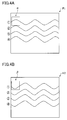
- FIG. 4A is a view schematically illustrating a first frame image F1 obtained by starting raster scanning at a timing that corresponds to the phase 0° of the device power supply alternating-current signal.
- FIG. 4B is a view schematically illustrating a second frame image F2 obtained by starting raster scanning at a timing that corresponds to the phase 180° of the device power supply alternating-current signal. Note that each line within the frame illustrated in FIGS. 4A and 4B represents the scanning line, and each number illustrated in FIGS. 4A and 4B is a number assigned to each scanning line.
- the scanning signal generator 20 supplies the scanning signal to the scanning deflector 13 at a timing that corresponds to the phase 0° of the device power supply alternating-current signal to obtain the first frame image F1 illustrated in FIG. 4A .
- the scanning signal generator 20 supplies the scanning signal to the scanning deflector 13 at a timing that corresponds to the phase 180° of the device power supply alternating-current signal to obtain the second frame image F2 illustrated in FIG. 4B .
- the first frame image F1 and the second frame image F2 are obtained by scanning the same measurement area of the specimen S with the electron beam B under the same measurement conditions, except that raster scanning is started at a different timing.
- the image displacement vector calculator 60 extracts an area that corresponds to the phase 90° of the device power supply alternating-current signal from the acquired first frame image F1 to obtain a first local frame image alpha (see FIG. 4A ).
- the image displacement vector calculator 60 extracts an area that corresponds to the phase 270° of the device power supply alternating-current signal from the acquired second frame image F2 to obtain a second local frame image beta (see FIG. 4B ).
- the area that corresponds to the phase 90° of the device power supply alternating-current signal refers to an area of the frame image that is obtained by scanning the specimen S with the electron beam B at a timing that corresponds to the phase 90° of the device power supply alternating-current signal. This also applies to an area that corresponds to the phase 180° and an area that corresponds to a phase other than 90° and 180°.
- FIG. 5A is a view schematically illustrating the first local frame image alpha
- FIG. 5B is a view schematically illustrating the second local frame image beta.
- the first local frame image alpha and the second local frame image beta are images that are formed around an area that corresponds to a phase that is shifted by 90° from the phase when raster scanning is started.
- the first local frame image alpha and the second local frame image beta are images that respectively represent the corresponding areas (i.e., areas that are identical in position and size within the frame) of the first frame image F1 and the second frame image F2. Therefore, the first local frame image alpha and the second local frame image beta are identical, when the electron beam B is not affected by the external disturbance magnetic field.
- the size of the first local frame image alpha and the second local frame image beta (the size of the area extracted from the first frame image F1 and the second frame image F2) may be set appropriately. For example, when the size of the first frame image F1 and the second frame image F2 is 1280x960 pixels, the size of the first local frame image alpha and the second local frame image beta is about 128x128 pixels.
- the phase 90° of the device power supply alternating-current signal corresponds to the ridge of the device power supply alternating-current signal where the amplitude of an external disturbance magnetic field that is synchronized with the device power supply alternating-current signal becomes a maximum. Therefore, the maximum image shift occurs corresponding to the phase 90° of the device power supply alternating-current signal.
- the electron beam B is shifted upward to the maximum extent at a timing that corresponds to the phase 90°, and the pattern of the first local frame image alpha is shifted downward to the maximum extent (see FIG. 5A ).
- the phase 270° of the device power supply alternating-current signal corresponds to the valley of the device power supply alternating-current signal where the amplitude of an external disturbance magnetic field that is synchronized with the device power supply alternating-current signal becomes a maximum in the direction opposite to the direction in which the amplitude of an external disturbance magnetic field becomes a maximum, when the phase of the device power supply alternating-current signal is 90°.
- the electron beam B is shifted downward to the maximum extent at a timing that corresponds to the phase 270°, and the pattern of the second local frame image beta is shifted upward to the maximum extent (see FIG. 5B ).
- the angle of the image displacement vector between the first local frame image alpha and the second local frame image beta corresponds to the angle of the external disturbance magnetic field
- the magnitude of the image displacement vector between the first local frame image alpha and the second local frame image beta corresponds to the magnitude of the external disturbance magnetic field.
- the image displacement vector between the first local frame image alpha and the second local frame image beta is a vector that represents the shift direction and the shift amount between the first local frame image alpha and the second local frame image beta.
- the image displacement vector calculator 60 calculates the image displacement vector G between the first local frame image alpha and the second local frame image beta.
- the image displacement vector calculator 60 calculates the image displacement vector G by performing a cross-correlation calculation process on the first local frame image alpha and the second local frame image beta.
- the cross-correlation calculation process calculates the inverse Fourier transform of the product of the complex conjugate of the two-dimensional Fourier transform of the first local frame image alpha and the second local frame image beta.
- the coordinates of the maximum value obtained by the two-dimensional cross-correlation calculation process are taken as the image displacement vector.
- the scanning correction signal generator 70 generates the scanning correction signal for correcting the scanning of the electron beam B based on the image displacement vector calculated by the image displacement vector calculator 60.
- FIG. 6 is a view illustrating the scanning correction signal.
- FIG. 6 illustrates the image displacement vector G in the scanning correction signal coordinate system (X, Y).
- the scanning correction signal generator 70 generates the scanning correction signal that produces an inverse vector from the angle theta and the magnitude H of the external disturbance magnetic field.
- the coordinate system of the scanning correction signal in the X-direction and the Y-direction is a coordinate system in which the origin is the scanning position (x, y) at a certain point represented by the uncorrected scanning signal (see 4A and 4B).
- the intensity G x of the external disturbance magnetic field in the X-direction is calculated by the following expression (1).
- G x - k H cos ⁇
- k is a device-specific constant. k may be set arbitrarily.
- the intensity G y of the external disturbance magnetic field in the Y-direction is calculated by the following expression (2).
- G y - k H sin ⁇
- the scanning correction signal is generated using the following sine function expressions (3) and (4) (X-direction and Y-direction).
- X G x sin 2 ⁇ x c
- Y G y sin 2 ⁇ x c
- C is a value determined from the cycle of the device power supply alternating-current signal that is known in advance.
- the scanning signal generator 20 adds the scanning correction signal generated by the scanning correction signal generator 70 to the scanning signal. Note that the intensity G x in the X-direction is 0 in the example illustrated in FIG. 6 .
- the scanning signal is indicated by the dotted line
- the results obtained by adding the scanning correction signal to the scanning signal are indicated by the solid line.
- the scanning correction signal is added to the scanning signal to correct the scanning signal.
- the scanning correction signal is added to only the scanning signal (y) since the intensity G x of the external disturbance magnetic field in the X-direction is 0. It is possible to reduce the shift of the image in the y-direction (vertical direction) that is synchronized with the device power supply alternating-current signal (see FIGS. 5A and 5B ) by adding the scanning correction signal to the scanning signal (y).
- FIG. 8 is a view illustrating an example of the results obtained by adding the scanning correction signal to the scanning signal when the intensity G x of the external disturbance magnetic field in the X-direction and the intensity G y of the external disturbance magnetic field in the Y-direction are not 0.
- the scanning signal is indicated by the dotted line
- the results obtained by adding the scanning correction signal to the scanning signal are indicated by the solid line.
- the scanning correction signal is respectively superimposed on the scanning signal (x) and the scanning signal (y). It is possible to reduce the expansion and contraction of the image in the x-direction that is synchronized with the device power supply alternating-current signal by superimposing the scanning correction signal on the scanning signal (x).
- the scanning signal generator 20 supplies the scanning signal to which the scanning correction signal is added to the scanning deflector 13 at a timing that corresponds to the phase 0° of the device power supply alternating-current signal, for example. This makes it possible to scan the electron beam B while deflecting the electron beam B so as to cancel the external disturbance magnetic field, and linearly scan the electron beam B.
- FIG. 9 is a flowchart illustrating an example of the image acquisition method that is implemented in the electron microscope 100 according to the first embodiment.
- the electron microscope 100 performs measurement scanning for acquiring the frame image F1 and the frame image F2 (step S10).
- the electron microscope 100 starts measurement scanning at a timing at which the scanning speed of the electron beam B is changed, for example. Measurement scanning may be carried out after the user has pressed a photographing start switch (not illustrated in the drawings), but before the photographing operation is performed, for example.
- the scanning signal generator 20 supplies the scanning signal to the scanning deflector 13 at a timing that corresponds to the phase 0° of the device power supply alternating-current signal to implement raster scanning corresponding to one frame, and then supplies the scanning signal to the scanning deflector 13 at a timing that corresponds to the phase 180° of the device power supply alternating-current signal to implement raster scanning corresponding to one frame.
- the frame image F1 is recorded in the frame memory 40 by implementing raster scanning at a timing that corresponds to the phase 0° of the device power supply alternating-current signal.
- the frame image F2 is recorded in the frame memory 40 by implementing raster scanning at a timing that corresponds to the phase 180° of the device power supply alternating-current signal.
- the image displacement vector calculator 60 extracts the first local frame image alpha from the frame image F1, and extracts the second local frame image beta from the frame image F2 (step S11).
- the image displacement vector calculator 60 then calculates the image displacement vector between the first local frame image alpha and the second local frame image beta (step S12).
- the scanning correction signal generator 70 generates the scanning correction signal based on the image displacement vector generated by the image displacement vector calculator 60 (step S13).
- the scanning signal generator 20 adds the scanning correction signal to the scanning signal, and supplies the scanning signal to which the scanning correction signal is added to the scanning deflector 13 (step S14).
- the scanning signal generator 20 supplies the scanning signal to which the scanning correction signal is added to the scanning deflector 13 at a timing that corresponds to the phase 0° of the device power supply alternating-current signal.
- the detection signal detected by the detector 16 is stored in the memory pixel that is included in the frame memory 40 and has an address that corresponds to the scanning position of the electron beam B in synchronization with the scanning signal to which the scanning correction signal is added.
- the image display device 50 reads the image data (the detection signal) stored in each memory pixel included in the frame memory 40, and displays an SEM image of the specimen S.
- An SEM image can be acquired by performing the above steps.
- the electron microscope 100 has the following features, for example.
- the electron microscope 100 is configured so that the image displacement vector calculator 60 calculates the image displacement vector between the first local frame image alpha and the second local frame image beta.
- the first local frame image alpha includes an area in the frame image F1 that is obtained by starting scanning at a timing that corresponds to the phase 0° of the device power supply alternating-current signal, and the area in the frame image F1 corresponds to the phase 90°.
- the second local frame image beta includes an area in the frame image F2 that is obtained by starting scanning at a timing that corresponds to the phase 180° of the device power supply alternating-current signal, and the area in the frame image F2 corresponds to the phase 270°.
- the scanning correction signal generator 70 generates the scanning correction signal based on the image displacement vector.
- the electron microscope 100 can correct the scanning signal based on the scanning correction signal, and scan the electron beam B while deflecting the electron beam B so as to cancel the external disturbance magnetic field. This makes it possible to reduce the cyclic distortion of the image that is caused by the external disturbance magnetic field and synchronized with the device power supply cycle, and acquire an accurate image for which the distortion is reduced.
- the electron microscope 100 can thus implement accurate observation and analysis.
- the electron microscope 100 is configured so that the first local frame image alpha includes an image that corresponds to the ridge of the device power supply alternating-current signal, and the second local frame image beta includes an image that corresponds to the valley of the device power supply alternating-current signal. This makes it possible to increase (maximize) the amount of shift between the first local frame image alpha and the second local frame image beta due to the external disturbance magnetic field. Therefore, the electron microscope 100 can more accurately calculate the direction and the magnitude of the image displacement vector, that is, the direction and the magnitude of the external disturbance magnetic field) using the image displacement vector calculator 60.
- the image acquisition method includes an image displacement vector calculation step (step S12) that calculates the image displacement vector between the first local frame image alpha and the second local frame image beta.
- the first local frame image alpha includes an area in the frame image F1 that is obtained by starting scanning at a timing that corresponds to the phase 0° of the device power supply alternating-current signal.
- the area in the frame image F1 corresponds to the phase 90°.
- the second local frame image beta includes an area in the frame image F2 that is obtained by starting scanning at a timing that corresponds to the phase 180° of the device power supply alternating-current signal, and the area in the frame image F2 corresponds to the phase 270°
- a scanning correction signal generation step step S13 that generates the scanning correction signal based on the image displacement vector. Therefore, it is possible to correct the scanning signal based on the scanning correction signal, and scan the electron beam B while deflecting the electron beam B so as to cancel the external disturbance magnetic field. This makes it possible to reduce the cyclic distortion of the image that is caused by the external disturbance magnetic field and synchronized with the device power supply cycle, and acquire an accurate image for which the distortion is reduced.
- the image acquisition method according to the first embodiment thus makes it possible to implement accurate observation and analysis.
- FIG. 10 is a view schematically illustrating the configuration of an electron microscope 200 according to the second embodiment. Note that the members of the electron microscope 200 according to the second embodiment that are identical in function to those of the electron microscope 100 according to the first embodiment are indicated by the same reference signs (symbols), and the description thereof is omitted.
- the electron microscope 100 is configured so that the scanning signal generator 20 uses the device power supply alternating-current signal as a signal with which raster scanning is synchronized (see FIG. 1 ).
- the electron microscope 200 includes a magnetic sensor 210 (see FIG. 10 ), and the scanning signal generator 20 uses an output signal from the magnetic sensor 210 as a signal with which raster scanning is synchronized.
- the magnetic sensor 210 can detect an external disturbance magnetic field.
- the magnetic sensor 210 is provided near the optical column of the electron microscope 200, for example.
- An image acquisition method that is implemented using the electron microscope 200 according to the second embodiment is the same as the image acquisition method that is implemented using the electron microscope 100 according to the first embodiment (see FIG. 9 ), except that the output signal from the magnetic sensor 210 is used instead of the device power supply alternating-current signal, and the description thereof is omitted.
- the electron microscope 200 according to the second embodiment and the image acquisition method that is implemented in the electron microscope 200 according to the second embodiment make it possible to reduce the cyclic distortion of the image that is caused by the external disturbance magnetic field, and acquire an accurate image for which the distortion is reduced in the same manner as the electron microscope 100 according to the first embodiment and the image acquisition method that is implemented in the electron microscope 100 according to the first embodiment.
- FIG. 11 is a view schematically illustrating the configuration of an electron microscope 300 according to the third embodiment. Note that the members of the electron microscope 300 according to the third embodiment that are identical in function to those of the electron microscope 100 according to the first embodiment are indicated by the same reference signs (symbols), and description thereof is omitted.
- the electron microscope 100 is configured so that the scanning signal generator 20 corrects the scanning signal by adding the scanning correction signal generated by the scanning correction signal generator 70 to the scanning signal to acquire an SEM image for which the distortion is reduced (see FIG. 1 ).
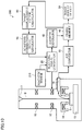
- the electron microscope 300 includes an address correction signal generator 310 (that is , an example of the address correction signal generation section) as shown in FIG. 11 , and the address generator 42 corrects the address of the memory pixel included in the frame memory 40 based on the address correction signal generated by the address correction signal generator 310, and stores the detection signal detected by the detector 16 in the memory pixel that has the corrected address to acquire an SEM image for which the distortion is reduced.
- an address correction signal generator 310 that is , an example of the address correction signal generation section
- the address correction signal generator 310 generates the address correction signal based on the image displacement vector calculated by the image displacement vector calculator 60 in the same manner as the scanning correction signal generator 70 (see FIG. 1 ).
- the address correction signal generator 310 generates the address correction signal that corrects the address of each memory pixel so that the scanning position of the electron beam B deflected by the external disturbance magnetic field corresponds to the address of the memory pixel from the angle theta and the magnitude H of the external disturbance magnetic field.
- the electron microscope 300 is configured so that the scanning signal generator 20 outputs the scanning signal (the scanning signal (x) that has a sawtooth-like signal waveform, and the scanning signal (y) that has a step-like signal waveform) to the scanning deflector 13 and the address generator 42 in synchronization with the device power supply alternating-current signal.
- the scanning signal generator 20 outputs the scanning signal (the scanning signal (x) that has a sawtooth-like signal waveform, and the scanning signal (y) that has a step-like signal waveform) to the scanning deflector 13 and the address generator 42 in synchronization with the device power supply alternating-current signal.
- the address generator 42 corrects the address of the memory pixel included in the frame memory 40 based on the address correction signal, and stores the detection signal detected by the detector 16 at the corrected address.
- the address generator 42 corrects the address that corresponds to the scanning signal from the scanning signal generator 20 based on the address correction signal to generate information about the new address.
- the address generator 42 outputs the address signal that includes the information about the new address to the frame memory 40.
- the detection signal is converted into a digital signal by the A/D converter 30, and stored in the memory pixel that has the address selected by the address signal.
- the selected address has been corrected so that the scanning position of the electron beam B corresponds to the address of the memory pixel.
- the detection signal is thus stored in the memory pixel that is included in the frame memory 40 and has the address that corresponds to the scanning position of the electron beam B.
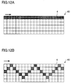
- FIG. 12A is a view illustrating the state of the frame memory 40 before the address is corrected
- FIG. 12B is a view illustrating the state of the frame memory 40 after the address is corrected.
- memory pixels 4 in which the detection signal is stored are indicated by the dark color.
- the detection signal is sequentially stored in the memory pixels 4 that are included in the frame memory 40 and arranged linearly corresponding to the scanning signal.
- the electron beam B is deflected by the external disturbance magnetic field, and the raster scanning lines are distorted cyclically, the resulting image is distorted, if the detection signal is sequentially stored in the memory pixels 4 that are arranged linearly corresponding to the scanning signal (see FIG. 12A ).
- the address generator 42 corrects the address of each memory pixel based on the address correction signal so that the scanning position of the electron beam B deflected by the external disturbance magnetic field corresponds to the address of the memory pixel (see FIG. 12B ). This makes it possible to reduce the cyclic distortion of the image caused by the external disturbance magnetic field.
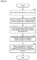
- FIG. 13 is a flowchart illustrating an example of the image acquisition method that is implemented in the electron microscope 300 according to the third embodiment.
- the electron microscope 300 performs measurement scanning for acquiring the frame image F1 and the frame image F2 (step S20).
- the image displacement vector calculator 60 extracts the first local frame image alpha from the frame image F1, and extracts the second local frame image beta from the frame image F2 (step S21).
- the image displacement vector calculator 60 then calculates the image displacement vector between the first local frame image alpha and the second local frame image beta (step S22).
- the steps S20 to S22 are respectively the same as the steps S10 to S12 illustrated in FIG. 9 , and description thereof is omitted.
- the address correction signal generator 310 generates the address correction signal based on the image displacement vector generated by the image displacement vector calculator 60 (step S23).
- the address generator 42 corrects the address of the memory pixel based on the address correction signal, and stores the detection signal at the corrected address (step S24).
- the scanning signal generator 20 outputs the scanning signal to the scanning deflector 13 and the address generator 42 in synchronization with the device power supply alternating-current signal.
- the address generator 42 corrects the address of the memory pixel that corresponds to the input scanning signal based on the address correction signal, and outputs the address signal to the frame memory 40.
- the detection signal is stored in the memory pixel that has the address selected by the address signal. The detection signal is thus stored in the memory pixel that is included in the frame memory 40 and has the address that corresponds to the scanning position of the electron beam B.
- the image display device 50 reads the image data (the detection signal) stored in each memory pixel included in the frame memory 40, and displays an SEM image of the specimen S.
- An SEM image can be acquired by performing the above steps.
- the electron microscope 300 is configured so that the image displacement vector calculator 60 calculates the image displacement vector between the first local frame image alpha and the second local frame image beta, the first local frame image alpha including an area in the frame image F1 that is obtained by starting scanning at a timing that corresponds to the phase 0° of the device power supply alternating-current signal, and the area in the frame image F1 corresponds to the phase 90°; the second local frame image beta including an area in the frame image F2 that is obtained by starting scanning at a timing that corresponds to the phase 180° of the device power supply alternating-current signal, and the area in the frame image F2 corresponds to the phase 270°, and the address correction signal generator 310 generates the address correction signal based on the image displacement vector.
- the electron microscope 300 can correct the address of the memory pixel included in the frame memory 40 based on the address correction signal so that the scanning position of the electron beam B deflected by the external disturbance magnetic field corresponds to the address of the memory pixel. This makes it possible to reduce the cyclic distortion of the image that is caused by the external disturbance magnetic field and synchronized with the device power supply cycle, and acquire an accurate image for which the distortion is reduced. The electron microscope 300 can thus implement accurate observation and analysis.
- the image acquisition method includes an image displacement vector calculation step (step S22) that calculates the image displacement vector between the first local frame image alpha and the second local frame image beta, the first local frame image alpha including an area in the frame image F1 that is obtained by starting scanning at a timing that corresponds to the phase 0° of the device power supply alternating-current signal, and the area in the frame image F1 corresponds to the phase 90°; the second local frame image beta including an area in the frame image F2 that is obtained by starting scanning at a timing that corresponds to the phase 180° of the device power supply alternating-current signal, and the area in the frame image F2 corresponds to the phase 270°, and an address correction signal generation step (step S23) that generates the address correction signal based on the image displacement vector.
- the image acquisition method according to the third embodiment thus makes it possible to implement accurate observation and analysis.
- the area that is extracted by the image displacement vector calculator 60 as the first local frame image alpha is not limited to an area that corresponds to the phase 90°, but may be an area that corresponds to an arbitrary phase other than the phase at which the intensity of the device power supply alternating-current signal becomes 0.
- the area that is extracted by the image displacement vector calculator 60 as the first local frame image alpha may be an area that corresponds to an arbitrary phase other than the phase 0° and the phase 180°.
- the area that is extracted by the image displacement vector calculator 60 as the second local frame image beta is not limited to an area that corresponds to the phase 270°, but may be an area that corresponds to an arbitrary phase other than the phase at which the intensity of the device power supply alternating-current signal becomes 0.
- the first local frame image alpha and the second local frame image beta be images that represent an area around a phase that is shifted by the same phase from the phase that corresponds to the timing at which raster scanning is started.
- the first local frame image alpha and the second local frame image beta are identical, when the electron beam B is not affected by the external disturbance magnetic field. Therefore, it is possible to more accurately calculate the direction and the magnitude of the external disturbance magnetic field from the image displacement vector between the first local frame image alpha and the second local frame image beta.
- the electron microscope according to the first modification can reduce the cyclic distortion of the image that is caused by the external disturbance magnetic field and synchronized with the device power supply cycle, and acquire an accurate image for which the distortion is reduced in the same manner as the electron microscope 100 according to the first embodiment, the electron microscope 200 according to the second embodiment, and the electron microscope 300 according to the third embodiment.
- the frame image F1 is an image obtained by starting raster scanning at a timing that corresponds to the phase 0° of the device power supply alternating-current signal (or the alternating-current signal from the magnetic sensor 210)
- the frame image F2 is an image obtained by starting raster scanning at a timing that corresponds to the phase 180° of the device power supply alternating-current signal.
- the phase that corresponds to the timing at which raster scanning is started may be an arbitrary phase as long as the frame image F1 and the frame image F2 are images obtained by starting raster scanning at a timing that corresponds to a different phase of the device power supply alternating-current signal.
- the electron microscope according to the second modification can reduce the cyclic distortion of the image that is caused by the external disturbance magnetic field and synchronized with the device power supply cycle, and acquire an accurate image for which the distortion is reduced in the same manner as the electron microscope 100 according to the first embodiment, the electron microscope 200 according to the second embodiment, and the electron microscope 300 according to the third embodiment.
- the invention includes various other configurations substantially the same as the configurations described in connection with the above embodiments (e.g., a configuration having the same function, method, and results, or a configuration having the same objective and effects).
- the invention also includes a configuration in which an unsubstantial element described in connection with the above embodiments is replaced by another element.
- the invention also includes a configuration having the same effects as those of the configurations described in connection with the above embodiments, or a configuration capable of achieving the same objective as that of the configurations described in connection with the above embodiments.
- the invention further includes a configuration in which a known technique is added to the configurations described in connection with the above embodiments.
Landscapes
- Chemical & Material Sciences (AREA)
- Analytical Chemistry (AREA)
- Electron Sources, Ion Sources (AREA)
- Analysing Materials By The Use Of Radiation (AREA)
- Testing Or Measuring Of Semiconductors Or The Like (AREA)
Applications Claiming Priority (1)
| Application Number | Priority Date | Filing Date | Title |
|---|---|---|---|
| JP2014245592A JP2016110767A (ja) | 2014-12-04 | 2014-12-04 | 荷電粒子ビーム装置および画像取得方法 |
Publications (1)
| Publication Number | Publication Date |
|---|---|
| EP3029710A1 true EP3029710A1 (de) | 2016-06-08 |
Family
ID=54780150
Family Applications (1)
| Application Number | Title | Priority Date | Filing Date |
|---|---|---|---|
| EP15197337.7A Withdrawn EP3029710A1 (de) | 2014-12-04 | 2015-12-01 | Ladungsträgerstrahlvorrichtung und bilderfassungsverfahren |
Country Status (4)
| Country | Link |
|---|---|
| US (1) | US20160163501A1 (de) |
| EP (1) | EP3029710A1 (de) |
| JP (1) | JP2016110767A (de) |
| KR (1) | KR20160067750A (de) |
Families Citing this family (4)
| Publication number | Priority date | Publication date | Assignee | Title |
|---|---|---|---|---|
| JP7299206B2 (ja) * | 2017-02-16 | 2023-06-27 | 株式会社荏原製作所 | 電子ビームの照射エリア調整方法および同調整システム、電子ビームの照射領域補正方法、ならびに、電子ビーム照射装置 |
| DE112021007695T5 (de) * | 2021-05-21 | 2024-03-07 | Mitsubishi Electric Corporation | Ic-rauschimmunitätserkennungsvorrichtung, ic-rauschimmunitätserkennungsverfahren und ic-innenimpedanzmessverfahren |
| KR20230147549A (ko) * | 2022-04-14 | 2023-10-23 | 에프이아이 컴파니 | 현미경 시스템의 간섭 보상 |
| US20250183002A1 (en) * | 2023-11-30 | 2025-06-05 | Fei Company | Scanning patterns for scientific instruments |
Citations (4)
| Publication number | Priority date | Publication date | Assignee | Title |
|---|---|---|---|---|
| US4791294A (en) * | 1986-10-08 | 1988-12-13 | Hitachi, Ltd. | Electron beam scanning method and scanning electron microscope |
| US4907287A (en) * | 1985-10-16 | 1990-03-06 | Hitachi, Ltd. | Image correction system for scanning electron microscope |
| JP2007149348A (ja) | 2005-11-24 | 2007-06-14 | Hitachi High-Technologies Corp | 走査電子顕微鏡 |
| JP2007324044A (ja) * | 2006-06-02 | 2007-12-13 | Hitachi High-Technologies Corp | 走査型荷電粒子線装置、その像表示方法、および走査型顕微鏡 |
Family Cites Families (9)
| Publication number | Priority date | Publication date | Assignee | Title |
|---|---|---|---|---|
| JPS6298544A (ja) * | 1985-10-25 | 1987-05-08 | Hitachi Ltd | 荷電粒子線装置 |
| US5225999A (en) * | 1990-07-06 | 1993-07-06 | The Trustees Of The University Of Pennsylvania | Magnetic environment stabilization for effective operation of magnetically sensitive instruments |
| JP3951590B2 (ja) * | 2000-10-27 | 2007-08-01 | 株式会社日立製作所 | 荷電粒子線装置 |
| JP4801518B2 (ja) * | 2006-07-07 | 2011-10-26 | 株式会社日立ハイテクノロジーズ | 荷電粒子線顕微方法および荷電粒子線装置 |
| JP5462434B2 (ja) * | 2007-07-13 | 2014-04-02 | 株式会社日立製作所 | 荷電粒子ビーム装置、及び荷電粒子ビーム顕微鏡 |
| JP5268532B2 (ja) * | 2008-09-30 | 2013-08-21 | 株式会社日立ハイテクノロジーズ | 試料計測方法、及び計測装置 |
| JP5537448B2 (ja) * | 2011-01-21 | 2014-07-02 | 株式会社日立ハイテクノロジーズ | 荷電粒子線装置、及び画像解析装置 |
| EP2667399A1 (de) * | 2012-05-23 | 2013-11-27 | FEI Company | Verbesserte Phasenplatte für ein TEM |
| US9177758B2 (en) * | 2013-03-25 | 2015-11-03 | Hermes Microvision Inc. | Charged particle beam apparatus |
-
2014
- 2014-12-04 JP JP2014245592A patent/JP2016110767A/ja active Pending
-
2015
- 2015-12-01 KR KR1020150170256A patent/KR20160067750A/ko not_active Withdrawn
- 2015-12-01 EP EP15197337.7A patent/EP3029710A1/de not_active Withdrawn
- 2015-12-03 US US14/957,734 patent/US20160163501A1/en not_active Abandoned
Patent Citations (4)
| Publication number | Priority date | Publication date | Assignee | Title |
|---|---|---|---|---|
| US4907287A (en) * | 1985-10-16 | 1990-03-06 | Hitachi, Ltd. | Image correction system for scanning electron microscope |
| US4791294A (en) * | 1986-10-08 | 1988-12-13 | Hitachi, Ltd. | Electron beam scanning method and scanning electron microscope |
| JP2007149348A (ja) | 2005-11-24 | 2007-06-14 | Hitachi High-Technologies Corp | 走査電子顕微鏡 |
| JP2007324044A (ja) * | 2006-06-02 | 2007-12-13 | Hitachi High-Technologies Corp | 走査型荷電粒子線装置、その像表示方法、および走査型顕微鏡 |
Also Published As
| Publication number | Publication date |
|---|---|
| JP2016110767A (ja) | 2016-06-20 |
| KR20160067750A (ko) | 2016-06-14 |
| US20160163501A1 (en) | 2016-06-09 |
Similar Documents
| Publication | Publication Date | Title |
|---|---|---|
| JP5948074B2 (ja) | 画像形成装置及び寸法測定装置 | |
| JP4801518B2 (ja) | 荷電粒子線顕微方法および荷電粒子線装置 | |
| EP3029710A1 (de) | Ladungsträgerstrahlvorrichtung und bilderfassungsverfahren | |
| US20110249110A1 (en) | Scanning electron microscope | |
| US10553391B2 (en) | SEM image acquisition device and SEM image acquisition method | |
| JP4512471B2 (ja) | 走査型電子顕微鏡及び半導体検査システム | |
| US9978558B2 (en) | Scanning-electron-microscope image processing device and scanning method | |
| KR102194151B1 (ko) | 하전 입자선 장치 | |
| WO2010095392A1 (ja) | 試料観察方法および走査電子顕微鏡 | |
| JP6770482B2 (ja) | 荷電粒子線装置および走査像の歪み補正方法 | |
| JP6130120B2 (ja) | 画像処理装置、画像処理方法、及びコンピュータ読取可能な記憶媒体 | |
| US11011346B2 (en) | Electron beam device and image processing method | |
| US9627175B2 (en) | Electron microscope and elemental mapping image generation method | |
| JP2018170166A (ja) | 荷電粒子線装置 | |
| US20060192119A1 (en) | Method of measurement accuracy improvement by control of pattern shrinkage | |
| JP7576592B2 (ja) | 荷電粒子線装置および画像取得方法 | |
| JP6078356B2 (ja) | テンプレートマッチング条件設定装置、及び荷電粒子線装置 | |
| JP6080565B2 (ja) | 荷電粒子線装置 | |
| JP6528035B2 (ja) | 電子顕微鏡 | |
| JP2564359B2 (ja) | パタ−ン検査方法及びパタ−ン測長方法並びに検査装置 | |
| JP2002075263A (ja) | 電子線装置 | |
| JPS6129645B2 (de) | ||
| JP7144485B2 (ja) | 像取得方法および電子顕微鏡 | |
| JPWO2020129164A1 (ja) | 撮像装置 | |
| JP4841407B2 (ja) | 電子顕微鏡 |
Legal Events
| Date | Code | Title | Description |
|---|---|---|---|
| PUAI | Public reference made under article 153(3) epc to a published international application that has entered the european phase |
Free format text: ORIGINAL CODE: 0009012 |
|
| AK | Designated contracting states |
Kind code of ref document: A1 Designated state(s): AL AT BE BG CH CY CZ DE DK EE ES FI FR GB GR HR HU IE IS IT LI LT LU LV MC MK MT NL NO PL PT RO RS SE SI SK SM TR |
|
| AX | Request for extension of the european patent |
Extension state: BA ME |
|
| 18D | Application deemed to be withdrawn |
Effective date: 20161209 |
|
| STAA | Information on the status of an ep patent application or granted ep patent |
Free format text: STATUS: THE APPLICATION IS DEEMED TO BE WITHDRAWN |