EP3035018A1 - Differenzieller temperatursensor - Google Patents
Differenzieller temperatursensor Download PDFInfo
- Publication number
- EP3035018A1 EP3035018A1 EP15201741.4A EP15201741A EP3035018A1 EP 3035018 A1 EP3035018 A1 EP 3035018A1 EP 15201741 A EP15201741 A EP 15201741A EP 3035018 A1 EP3035018 A1 EP 3035018A1
- Authority
- EP
- European Patent Office
- Prior art keywords
- sensor
- support member
- connection
- source
- substrate
- Prior art date
- Legal status (The legal status is an assumption and is not a legal conclusion. Google has not performed a legal analysis and makes no representation as to the accuracy of the status listed.)
- Granted
Links
Images


Classifications
-
- H—ELECTRICITY
- H10—SEMICONDUCTOR DEVICES; ELECTRIC SOLID-STATE DEVICES NOT OTHERWISE PROVIDED FOR
- H10N—ELECTRIC SOLID-STATE DEVICES NOT OTHERWISE PROVIDED FOR
- H10N10/00—Thermoelectric devices comprising a junction of dissimilar materials, i.e. devices exhibiting Seebeck or Peltier effects
- H10N10/10—Thermoelectric devices comprising a junction of dissimilar materials, i.e. devices exhibiting Seebeck or Peltier effects operating with only the Peltier or Seebeck effects
- H10N10/17—Thermoelectric devices comprising a junction of dissimilar materials, i.e. devices exhibiting Seebeck or Peltier effects operating with only the Peltier or Seebeck effects characterised by the structure or configuration of the cell or thermocouple forming the device
-
- G—PHYSICS
- G01—MEASURING; TESTING
- G01K—MEASURING TEMPERATURE; MEASURING QUANTITY OF HEAT; THERMALLY-SENSITIVE ELEMENTS NOT OTHERWISE PROVIDED FOR
- G01K1/00—Details of thermometers not specially adapted for particular types of thermometer
- G01K1/16—Special arrangements for conducting heat from the object to the sensitive element
- G01K1/18—Special arrangements for conducting heat from the object to the sensitive element for reducing thermal inertia
-
- G—PHYSICS
- G01—MEASURING; TESTING
- G01K—MEASURING TEMPERATURE; MEASURING QUANTITY OF HEAT; THERMALLY-SENSITIVE ELEMENTS NOT OTHERWISE PROVIDED FOR
- G01K17/00—Measuring quantity of heat
- G01K17/06—Measuring quantity of heat conveyed by flowing media, e.g. in heating systems e.g. the quantity of heat in a transporting medium, delivered to or consumed in an expenditure device
- G01K17/08—Measuring quantity of heat conveyed by flowing media, e.g. in heating systems e.g. the quantity of heat in a transporting medium, delivered to or consumed in an expenditure device based upon measurement of temperature difference or of a temperature
- G01K17/20—Measuring quantity of heat conveyed by flowing media, e.g. in heating systems e.g. the quantity of heat in a transporting medium, delivered to or consumed in an expenditure device based upon measurement of temperature difference or of a temperature across a radiating surface, combined with ascertainment of the heat-transmission coefficient
-
- G—PHYSICS
- G01—MEASURING; TESTING
- G01K—MEASURING TEMPERATURE; MEASURING QUANTITY OF HEAT; THERMALLY-SENSITIVE ELEMENTS NOT OTHERWISE PROVIDED FOR
- G01K3/00—Thermometers giving results other than momentary value of temperature
- G01K3/08—Thermometers giving results other than momentary value of temperature giving differences of values; giving differentiated values
- G01K3/14—Thermometers giving results other than momentary value of temperature giving differences of values; giving differentiated values in respect of space
-
- G—PHYSICS
- G01—MEASURING; TESTING
- G01K—MEASURING TEMPERATURE; MEASURING QUANTITY OF HEAT; THERMALLY-SENSITIVE ELEMENTS NOT OTHERWISE PROVIDED FOR
- G01K7/00—Measuring temperature based on the use of electric or magnetic elements directly sensitive to heat ; Power supply therefor, e.g. using thermoelectric elements
- G01K7/02—Measuring temperature based on the use of electric or magnetic elements directly sensitive to heat ; Power supply therefor, e.g. using thermoelectric elements using thermoelectric elements, e.g. thermocouples
- G01K7/028—Measuring temperature based on the use of electric or magnetic elements directly sensitive to heat ; Power supply therefor, e.g. using thermoelectric elements using thermoelectric elements, e.g. thermocouples using microstructures, e.g. made of silicon
-
- H—ELECTRICITY
- H10—SEMICONDUCTOR DEVICES; ELECTRIC SOLID-STATE DEVICES NOT OTHERWISE PROVIDED FOR
- H10N—ELECTRIC SOLID-STATE DEVICES NOT OTHERWISE PROVIDED FOR
- H10N10/00—Thermoelectric devices comprising a junction of dissimilar materials, i.e. devices exhibiting Seebeck or Peltier effects
- H10N10/80—Constructional details
- H10N10/81—Structural details of the junction
Definitions
- the present invention relates to a differential temperature sensor. More specifically, it is a thermoelectric sensor Seebeck effect.
- hot and cold mean relatively, that is, the temperature of the "hot” source is greater than the temperature of the "cold” source.
- connection pads are intended to be thermally connected to the hot source Sc and the cold source Sf.
- the set of thermoelectric layers comprises N thermocouples 100, 101, that is to say N layers made from a first thermoelectric material 100 and N layers made from a second thermoelectric material 101.
- Each first junction 10 and each second junction 11 is formed of an electrically conductive material.
- Such a sensor 1 of the state of the art forms a chip, and is part of the thin film technologies, thus differing from the macroscopic Seebeck thermoelectric effect sensors.
- chip is meant a wafer, preferably of silicon, comprising an elementary component.
- Such a sensor 1 of the state of the art is therefore used in various applications where miniaturization is sought.
- Non-restrictive examples include microelectronics, mobile telephony, home automation ( smart home , smart building , smart building , Smart Grids) and certain industrial processes.
- connection of the support member with the hot and cold sources can be direct, that is to say that the support member is in direct contact with said sources.
- the connection may be indirect, that is to say that the support member is thermally connected to said sources via a thermal path.
- thermal insulating is meant that the support member has a thermal conductivity lower than a value of the order of 150 W / m / K.
- Thermally conductive means an entity having a thermal conductivity greater than a value of the order of 150 W / m / K.
- the support member is thermally insulating so as to avoid the formation of a thermal bridge between the first and the second metal connection means via the support member.
- the thermal gradient between the hot source and the cold source can be passed between the first and the second metallic connection means, and therefore between the hot side and the cold side of the set of thermoelectric layers via the first one. and the second connection pads.
- thermal losses associated with the integration are greatly reduced by means of heat transfer means of the support member and the first and second metal connection means.
- the first and second metal connection means comprise a brazing soldered respectively on the or each first connection pad and on the or each second connection pad so as to assemble the substrate and the support.
- the first and second metal connection means comprise a wiring wire welded respectively to the or each first connection pad and to the or each second connection pad so as to assemble the substrate and the body of support.
- the heat transfer means comprise at least a first and a second metal connection pins intended to be respectively connected to the hot source and the cold source.
- the senor comprises an integrated circuit package enclosing the set of thermoelectric layers, said housing comprising the support member.
- an integrated circuit package conventionally comprises metal connection pins connectable to the hot source and the cold source.
- an integrated circuit package encapsulates the set of thermoelectric layers.
- Non-integrated planar sensors capable of performing temperature measurements of a flow orthogonal to the substrate are known from the state of the art, including documents WO 2007034048 , FR 2955708 , WO 8402037 and FR 2598803 .
- additional box allows the measurement of temperature when the hot and cold sources are arranged on either side of the integrated circuit package in a plane orthogonal to the substrate, and while maintaining a sensor chip integrated.
- the thickness and the first and second faces of the additional box are adapted to the distance between the hot and cold sources, the dimensions of the integrated circuit package can then be fixed.
- the thermally conductive faces and the vias transfer heat between the hot and cold sources and the integrated circuit package.
- the additional box comprises a support member arranged to support the integrated circuit package.
- the support member of the additional box makes it possible to improve the mechanical strength of the sensor.
- the integrated circuit package comprises at least one electrical connection pin
- the additional box comprises at least one electrical track extending from the electrical connection pin
- the senor comprises an encapsulation layer arranged on the support member so as to encapsulate the set of thermoelectric layers, the encapsulation layer being preferably made of a material based on a polymer.
- the set of thermoelectric layers has a free surface
- the sensor comprises a first and a second thermally conductive elements extending opposite and at a distance from said surface. free, and in the extension respectively of the hot side and the cold side of said assembly.
- thermally conductive elements make it possible to homogenize the heat transfer between the hot side and the cold side of the set of thermoelectric layers.
- the senor comprises a dielectric layer interposed between the substrate and the set of thermoelectric layers.
- Such a dielectric layer makes it possible to isolate the substrate electrically and thermally.
- the substrate is made of a material based on silicon.
- the substrate is made of a thermally insulating material, such as glass or quartz.
- hot and cold mean relatively, that is, the temperature of the "hot” source is greater than the temperature of the "cold” source.
- Such a sensor 1 forms a chip that is to say a substrate wafer, preferably in a silicon-based material, comprising an elementary component.
- the structure formed by the substrate 3, the set E of thermoelectric layers and the connection pads 50, 51 will be called "chip-sensor”.
- the substrate 3 is advantageously plane.
- the substrate 3 advantageously has a thickness of between 100 and 200 ⁇ m in order to limit the heat transfer towards the substrate 3.
- first direction is the direction that extends along the thickness of the substrate 3.
- the set of thermoelectric layers comprises N thermocouples 100, 101, that is to say N layers made from a first thermoelectric material 100 and N layers made from a second thermoelectric material 101.
- the first thermoelectric material 100 is advantageously electrically doped according to a first type of conductivity.
- the second thermoelectric material 101 is advantageously doped according to a second type of conductivity.
- Each first junction 10 and each second junction 11 are formed of an electrically conductive material.
- the N thermocouples 100, 101 and the thermally insulating material 102 are juxtaposed in a direction perpendicular to the first direction.
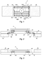
- the sensor 1 comprises a support member 2 arranged to support the substrate.
- the support member 2 is intended to be connected directly or indirectly to the hot source Sc and to the cold source Sf.
- the support member 2 is made of a thermally insulating material.
- the sensor 1 comprises first and second metallic connection means arranged to electrically connect the support member 2 with respectively the or each first connection pad 50 and the or each second connection pad 51.
- the support member 2 comprises heat transfer means arranged to transfer heat from the hot source Sc to the first metal connection means, and to transfer the heat of the second metal connection means to the cold source Sf.
- the first metal connection means comprise a soldering ball 20 brazed to each first connection pad 50.
- the second metal connection means comprise a brazing solder ball 21 on each second connection pad 51.
- the balls of brazing 20, 21 also makes it possible to assemble the substrate 3 and the support member 2.
- the sensor 1 may comprise additional solder balls 22 (visible at figure 6 ) which are not electrically connected to the connection pads 50, 51 but contribute to assemble the substrate 3 with the support member 2 to improve the mechanical strength.
- the solder balls 20, 21, 22 are preferably made of a material selected from the group consisting of Au, SnAgAu, SnAgCu.
- Brazing balls 20, 21, 22 advantageously have a diameter of about 80 microns for a thickness of about 80 microns. Such dimensions make it possible to combine compactness and heat transfer area sufficient for the functionality of the sensor 1.
- the diameter and the thickness of the solder balls 20, 21, 22 may vary, for example between a few tens and a few hundred microns.
- the first and second metallic connection means comprise a wiring wire 20, 21 respectively welded to each first connection pad 50 and to each second connection pad 51 so as to assemble the substrate 3 and the support member 2.
- the hot source Sc and the cold source Sf can be arranged on the support member 2 ( figures 3 and 5 ).
- the hot source Sc and the cold source Sf can be arranged under the support member 2 ( figures 2 and 4 ).
- such metal tracks 40, 41 have a thickness of the order of a few tens of nm for a thickness of the support member 2 of the order of 100 nm.
- the support member 2 may be a transfer substrate adapted to postpone the sensor chip.
- the sensor chip can be encapsulated using an encapsulation layer 5 arranged on the support member 2 so as to encapsulate the assembly E.
- the encapsulation layer 5 is made based on a thermally insulating material.
- the encapsulation layer 5 is preferably made of a polymer-based material.
- the support member 2 belongs to a housing 6 of integrated circuit.
- the first and second connection pins 30, 31 equip the housing 6.
- the housing 6 may be SMD ( Surface Mounted Device ) type.
- the housing 6 is preferably made of thermally insulating material.
- the housing 6 preferably has a thickness of between 0.1 and a few mm.
- the housing 6 does not preferably have a central metal surface conventionally used as a heat sink so as not to interfere with the heat transfer between the housing 6 and the sensor chip.
- connection pins 30, 31 may be continuous to form bars.
- connection can be direct, that is to say that the connection pins 30, 31 are respectively in direct contact with the hot source Sc and the cold source Sf.
- connection can be indirect, that is to say say that the connection pins 30, 31 are thermally connected to said sources via a thermal path CT.
- the first connection pins 30 form heat transfer means arranged to transfer the heat from the hot source Sc to the first metal tracks 40.
- the second connection pins 31 form heat transfer means arranged to transfer the heat of the second metal tracks 41 to the cold source Sf.
- the housing 6 has additional rows of metal connection pins 32 which are not used as heat transfer means.
- the additional metal connection pins 32 are used as simple electrical connectors.
- the sensor chip may comprise electrical connection pads electrically connected to each first junction and each second junction.
- the connection pins 32 may be electrically connected to said electrical connection pads.
- Those skilled in the art can choose different arrangements for the connection pins 30, 31 used as heat transfer means, and for the connection pins 32 used as electrical connectors. These different arrangements will be chosen in particular according to the intended application, the positioning of hot and cold sources Sc, Sf, and connectors for the integration of the sensor chip. It is also possible to use at least one metal connection pin both as an electrical connector and as a heat transfer means.
- the substrate 3 and the support member 2 belonging to the housing 6 are advantageously assembled by the process of the flip chip ( Flip-Chip in English), known to those skilled in the art, when the metal connection means comprise balls. brazing 20, 21, 22.
- the substrate 3 and the support member 2 belonging to the housing 6 are advantageously assembled by the wire bonding method , known to those skilled in the art, when the metal connection means comprise Wiring 20, 21 welded ( figure 12 ).
- the housing 6 may be connected to an electronic card 70, for example of the SMI (Isolated Metal Substrate) type.
- the hot and cold sources Sc, Sf are arranged at the rear of the electronic card 70 and are thermally connected to the wiring son 20, 21 welded.
- the additional housing 8 is advantageously made of a thermally insulating material.
- the faces 8a, 8b are made thermally conductive preferably by means of a coating based on a thermally conductive material.
- the thermally conductive material of the coating may be a metal such as Cu, Au, Ag, or a silver-based alloy, or a material selected from the group consisting of SiC, AlN, Al anodized.
- the thermally conductive material of the coating may be deposited on the additional box 8 according to various techniques such as chemical vapor deposition (CVD) or physical vapor deposition (PVD).
- CVD chemical vapor deposition
- PVD physical vapor deposition
- the thermally conductive material of the coating can be welded or brazed directly onto the additional housing 8.
- the vias 80, 81 may have different shapes.
- the vias 80, 81 may be monoblock or formed into several wells.
- the vias 80, 81 may be connected directly to the connection pins 30, 31 or indirectly via metal tracks.
- the additional box 8 advantageously comprises a support member 9 arranged to support the integrated circuit package 6 inside the additional box 8.
- the integrated circuit package 6 is advantageously fixed to the support member 9 of the additional box 8 by bonding, brazing or welding.
- the support member 9 of the additional housing 8 has orifices provided therein to receive the second via 81.
- the additional housing 8 is advantageously made of a thermally insulating material so as to avoid the formation of a thermal bridge between the first via 80 and the second through 81 via the support member 9 of the additional housing 8.
- the enclosure delimited by the additional housing 8 may advantageously be evacuated in order to concentrate the heat transfer on the vias 80, 81.
- lateral means a direction parallel to the first direction, that is to say the direction extending along the thickness of the substrate 3.
- the following table gathers parameters enabling the first via 80 as well as the support member 9 of the additional box 8 to be correctly geometrically configured: Parameter e supp 200 ⁇ m e via 700 ⁇ m ⁇ supp 0.2 W / m / K (epoxy resin) ⁇ via 386 W / m / K (Cu) S supp 5x5 mm 2 S via 3x1 mm 2 ⁇ 66
- the integrated circuit package 6 advantageously comprises at least one electrical connection pin 32 which is not used as heat transfer means.
- the additional box 8 advantageously comprises at least one electrical track 90 extending from the electrical connection pin 32.
- the person skilled in the art can choose different arrangements for the electrical connection pins 32, particularly as a function of the application envisaged, of the positioning of the hot and cold sources Sc, Sf, Thus, the person skilled in the art can choose different arrangements for the tracks.
- electrical 90 according to the arrangements of said electrical connection pins 32 to define different electrical output positions for the additional box 8.
- the or each electrical track 90 is advantageously formed in the support member 9 of the additional housing 8.
- the set E of thermoelectric layers has a free surface S L
- the sensor comprises a first and a second thermally conductive element 7a, 7b extending opposite and at a distance from said free surface S L , and in the extension respectively of the side and the cold side of said set E.
- the first and second thermally conductive elements 7a, 7b surmount lateral zones of the free surface S L without direct contact.
- the first and second thermally conductive elements 7a, 7b may be made of any thermally conductive material, as described in the document WO 2011012586 .
- the first and second thermally conductive elements 7a, 7b are advantageously metallic.
- the first and second thermally conductive elements 7a, 7b are advantageously made in the form of a metal strip.
- the senor 1 comprises a dielectric layer interposed between the substrate 3 and the set E of thermoelectric layers.
- the dielectric layer is advantageously SiO 2 or Si 3 N 4 .
- the dielectric layer has a thickness of between a few nm and several hundreds of ⁇ m.
Landscapes
- Physics & Mathematics (AREA)
- General Physics & Mathematics (AREA)
- Chemical & Material Sciences (AREA)
- Crystallography & Structural Chemistry (AREA)
- Engineering & Computer Science (AREA)
- Combustion & Propulsion (AREA)
- Measuring Temperature Or Quantity Of Heat (AREA)
- Investigating Or Analyzing Materials Using Thermal Means (AREA)
Applications Claiming Priority (1)
| Application Number | Priority Date | Filing Date | Title |
|---|---|---|---|
| FR1462975A FR3030734B1 (fr) | 2014-12-19 | 2014-12-19 | Capteur differentiel de temperature. |
Publications (2)
| Publication Number | Publication Date |
|---|---|
| EP3035018A1 true EP3035018A1 (de) | 2016-06-22 |
| EP3035018B1 EP3035018B1 (de) | 2017-10-18 |
Family
ID=52627437
Family Applications (1)
| Application Number | Title | Priority Date | Filing Date |
|---|---|---|---|
| EP15201741.4A Active EP3035018B1 (de) | 2014-12-19 | 2015-12-21 | Differenzieller temperatursensor |
Country Status (5)
| Country | Link |
|---|---|
| US (1) | US10038133B2 (de) |
| EP (1) | EP3035018B1 (de) |
| JP (1) | JP6912858B2 (de) |
| CA (1) | CA2915853C (de) |
| FR (1) | FR3030734B1 (de) |
Families Citing this family (3)
| Publication number | Priority date | Publication date | Assignee | Title |
|---|---|---|---|---|
| CA3013913A1 (en) * | 2016-02-08 | 2017-08-17 | Mtpv Power Corporation | Radiative micron-gap thermophotovoltaic system with transparent emitter |
| CN106725354A (zh) * | 2016-12-06 | 2017-05-31 | 东莞市宇朔泰合健康科技有限公司 | 一种快速热平衡内置ad转换的体温传感器结构 |
| CN114730778A (zh) * | 2019-12-27 | 2022-07-08 | 索尼半导体解决方案公司 | 传感器装置 |
Citations (8)
| Publication number | Priority date | Publication date | Assignee | Title |
|---|---|---|---|---|
| WO1984002037A1 (fr) | 1982-11-18 | 1984-05-24 | Anvar | Fluxmetre thermique a thermocouples |
| FR2598803A1 (fr) | 1986-05-16 | 1987-11-20 | Anvar | Dispositif pour mesurer l'intensite d'un flux radiatif |
| US20060076046A1 (en) * | 2004-10-08 | 2006-04-13 | Nanocoolers, Inc. | Thermoelectric device structure and apparatus incorporating same |
| WO2007034048A1 (fr) | 2005-09-22 | 2007-03-29 | Universite Des Sciences Et Technologies De Lille | Microcapteur de flux thermique sur substrat conducteur avec caisson(s) poreux |
| EP1976034A2 (de) * | 2007-03-29 | 2008-10-01 | Stichting IMEC Nederland | Herstellungsverfahren für eine Thermosäule, damit hergestellte Thermosäule und thermoelektrischer Generator mit solchen Thermosäulen |
| WO2011012586A1 (fr) | 2009-07-29 | 2011-02-03 | St-Ericsson (Grenoble) Sas | Dispositif thermoelectrique en technologie de semi-conducteurs |
| FR2955708A1 (fr) | 2010-01-25 | 2011-07-29 | Univ Lille 1 Sciences & Technologies | Microgenerateur de tension utilisant la chaleur latente de changement de phase d'un liquide |
| WO2013007593A1 (fr) * | 2011-07-13 | 2013-01-17 | Stmicroelectronics (Rousset) Sas | Procédé de génération d'énergie électrique au sein d'une structure intégrée tridimensionnelle, et dispositif de liaison correspondant |
Family Cites Families (18)
| Publication number | Priority date | Publication date | Assignee | Title |
|---|---|---|---|---|
| JPS499794B1 (de) * | 1969-02-13 | 1974-03-06 | ||
| DE3134166A1 (de) * | 1981-08-28 | 1983-03-10 | Robert Bosch Gmbh, 7000 Stuttgart | Temperaturfuehler |
| JPS60118932U (ja) * | 1984-01-13 | 1985-08-12 | 住田 康寿 | 端子付端子板 |
| JP2636119B2 (ja) * | 1992-09-08 | 1997-07-30 | 工業技術院長 | 熱電素子シートとその製造方法 |
| JPH11183270A (ja) * | 1997-12-10 | 1999-07-09 | Interuniv Micro Electron Centrum Vzw | 熱検知デバイスおよび方法 |
| JP3728198B2 (ja) * | 2000-11-10 | 2005-12-21 | 新日本製鐵株式会社 | 評価対象の状態検出装置、状態検出方法およびコンピュータ読み取り可能な記録媒体 |
| JP4041279B2 (ja) * | 2000-11-10 | 2008-01-30 | 新日本製鐵株式会社 | 鋳型内鋳片の状態検知装置、方法、及びコンピュータ読み取り可能な記憶媒体 |
| US20050034749A1 (en) * | 2003-08-12 | 2005-02-17 | Chung-Nan Chen | Structure of thermopile sensor |
| JP4482667B2 (ja) * | 2004-09-13 | 2010-06-16 | 独立行政法人産業技術総合研究所 | 冷却効果を持つ配線構造 |
| TWI405361B (zh) * | 2008-12-31 | 2013-08-11 | 財團法人工業技術研究院 | 熱電元件及其製程、晶片堆疊結構及晶片封裝結構 |
| JP2012181090A (ja) * | 2011-03-01 | 2012-09-20 | Nippon Soken Inc | 熱流束センサ |
| JP5769009B2 (ja) * | 2011-06-09 | 2015-08-26 | 江藤電気株式会社 | 熱流センサ及び熱流センサの製造方法 |
| JP5804366B2 (ja) * | 2011-08-26 | 2015-11-04 | 株式会社リコー | 温度測定装置 |
| KR101928005B1 (ko) * | 2011-12-01 | 2019-03-13 | 삼성전자주식회사 | 열전 냉각 패키지 및 이의 열관리 방법 |
| JP6047413B2 (ja) * | 2013-01-29 | 2016-12-21 | 富士フイルム株式会社 | 熱電発電モジュール |
| JP2014163428A (ja) * | 2013-02-22 | 2014-09-08 | Mitsubishi Heavy Ind Ltd | 積層部材、該積層部材の製造方法、該積層部材を用いた軸受パッド、該軸受パッドと有する軸受装置、及び該軸受装置を備えた回転機械 |
| US9719867B2 (en) * | 2013-05-30 | 2017-08-01 | Kla-Tencor Corporation | Method and system for measuring heat flux |
| FR3030889B1 (fr) * | 2014-12-19 | 2017-01-27 | Commissariat Energie Atomique | Capteur differentiel de temperature. |
-
2014
- 2014-12-19 FR FR1462975A patent/FR3030734B1/fr not_active Expired - Fee Related
-
2015
- 2015-12-18 CA CA2915853A patent/CA2915853C/fr active Active
- 2015-12-18 JP JP2015247914A patent/JP6912858B2/ja not_active Expired - Fee Related
- 2015-12-18 US US14/975,078 patent/US10038133B2/en active Active
- 2015-12-21 EP EP15201741.4A patent/EP3035018B1/de active Active
Patent Citations (8)
| Publication number | Priority date | Publication date | Assignee | Title |
|---|---|---|---|---|
| WO1984002037A1 (fr) | 1982-11-18 | 1984-05-24 | Anvar | Fluxmetre thermique a thermocouples |
| FR2598803A1 (fr) | 1986-05-16 | 1987-11-20 | Anvar | Dispositif pour mesurer l'intensite d'un flux radiatif |
| US20060076046A1 (en) * | 2004-10-08 | 2006-04-13 | Nanocoolers, Inc. | Thermoelectric device structure and apparatus incorporating same |
| WO2007034048A1 (fr) | 2005-09-22 | 2007-03-29 | Universite Des Sciences Et Technologies De Lille | Microcapteur de flux thermique sur substrat conducteur avec caisson(s) poreux |
| EP1976034A2 (de) * | 2007-03-29 | 2008-10-01 | Stichting IMEC Nederland | Herstellungsverfahren für eine Thermosäule, damit hergestellte Thermosäule und thermoelektrischer Generator mit solchen Thermosäulen |
| WO2011012586A1 (fr) | 2009-07-29 | 2011-02-03 | St-Ericsson (Grenoble) Sas | Dispositif thermoelectrique en technologie de semi-conducteurs |
| FR2955708A1 (fr) | 2010-01-25 | 2011-07-29 | Univ Lille 1 Sciences & Technologies | Microgenerateur de tension utilisant la chaleur latente de changement de phase d'un liquide |
| WO2013007593A1 (fr) * | 2011-07-13 | 2013-01-17 | Stmicroelectronics (Rousset) Sas | Procédé de génération d'énergie électrique au sein d'une structure intégrée tridimensionnelle, et dispositif de liaison correspondant |
Also Published As
| Publication number | Publication date |
|---|---|
| JP6912858B2 (ja) | 2021-08-04 |
| CA2915853A1 (fr) | 2016-06-19 |
| CA2915853C (fr) | 2023-07-11 |
| FR3030734B1 (fr) | 2017-01-27 |
| US10038133B2 (en) | 2018-07-31 |
| EP3035018B1 (de) | 2017-10-18 |
| US20160181502A1 (en) | 2016-06-23 |
| JP2016118554A (ja) | 2016-06-30 |
| FR3030734A1 (fr) | 2016-06-24 |
Similar Documents
| Publication | Publication Date | Title |
|---|---|---|
| US6084172A (en) | Thermoelectric conversion component | |
| EP3035017B1 (de) | Differenzieller temperatursensor | |
| EP2689221B1 (de) | Differenzialtemperatursensor und seine cmos/bicmos-technologiekompetenzen | |
| EP3035018B1 (de) | Differenzieller temperatursensor | |
| FR3018953A1 (fr) | Puce de circuit integre montee sur un interposeur | |
| EP1792526B1 (de) | Mit integriertem wärmeverteiler ausgestattete elektronische einrichtung | |
| WO2018091852A1 (fr) | Circuit intégré forme de deux puces connectées en série | |
| JP6851773B2 (ja) | 半導体装置 | |
| EP2750183B1 (de) | Integrierter Schaltkreis, und Herstellungsverfahren eines integrierten Schaltkreises, der mit einer Temperatursonde ausgestattet ist | |
| FR2511193A1 (fr) | Support en materiau colamine pour le refroidissement et l'encapsulation d'un substrat de circuit electronique | |
| EP1427008B1 (de) | Herstellungsverfahren für einen elektronischen Modul mit einem aktiven Bauteil auf einem Substrat | |
| EP0619616B1 (de) | Peltiereffektapparat zur Detektion der Wahrscheinlichkeit von Kondensationsbildung an einer Oberfläche, die sich in Kontakt mit feuchter Luft befindet | |
| FR2783969A1 (fr) | Dispositif hybride et procede de realisation de composants electriquement actifs par assemblage | |
| EP4409246B1 (de) | Dünnes kompaktes thermoelement und verfahren zur herstellung eines solchen thermoelements | |
| FR3002085A1 (fr) | Composant incluant un element de conversion d'energie | |
| EP4355063B1 (de) | Verfahren zur metallisierung einer thermoelektrischen struktur | |
| CN105405813B (zh) | 电子构件 | |
| EP2315243A1 (de) | Interposer zwischen integrierten Schaltkreisen | |
| FR3002084A1 (fr) | Structure electronique incluant un element de conversion d'energie | |
| FR3147930A1 (fr) | Equipement électronique comprenant au moins un module thermoélectrique, système électronique correspondant | |
| FR3053528A1 (fr) | Dispositif electronique ayant une banque integree de composants passifs | |
| EP4355062A1 (de) | Verfahren zur herstellung einer thermoelektrischen struktur | |
| FR3162911A1 (fr) | Fabrication d’un module de puissance | |
| EP2645436A1 (de) | Leuchtdiodenbauteil mit niedrigem Wärmewiderstand mit getrennten elektronischen und thermischen Leiterbahnen | |
| FR2716302A1 (fr) | Dispositif de chauffage pour la réalisation de connexions par un matériau fusible. |
Legal Events
| Date | Code | Title | Description |
|---|---|---|---|
| PUAI | Public reference made under article 153(3) epc to a published international application that has entered the european phase |
Free format text: ORIGINAL CODE: 0009012 |
|
| AK | Designated contracting states |
Kind code of ref document: A1 Designated state(s): AL AT BE BG CH CY CZ DE DK EE ES FI FR GB GR HR HU IE IS IT LI LT LU LV MC MK MT NL NO PL PT RO RS SE SI SK SM TR |
|
| AX | Request for extension of the european patent |
Extension state: BA ME |
|
| STAA | Information on the status of an ep patent application or granted ep patent |
Free format text: STATUS: REQUEST FOR EXAMINATION WAS MADE |
|
| 17P | Request for examination filed |
Effective date: 20161123 |
|
| RBV | Designated contracting states (corrected) |
Designated state(s): AL AT BE BG CH CY CZ DE DK EE ES FI FR GB GR HR HU IE IS IT LI LT LU LV MC MK MT NL NO PL PT RO RS SE SI SK SM TR |
|
| GRAP | Despatch of communication of intention to grant a patent |
Free format text: ORIGINAL CODE: EPIDOSNIGR1 |
|
| STAA | Information on the status of an ep patent application or granted ep patent |
Free format text: STATUS: GRANT OF PATENT IS INTENDED |
|
| INTG | Intention to grant announced |
Effective date: 20170426 |
|
| GRAS | Grant fee paid |
Free format text: ORIGINAL CODE: EPIDOSNIGR3 |
|
| GRAA | (expected) grant |
Free format text: ORIGINAL CODE: 0009210 |
|
| STAA | Information on the status of an ep patent application or granted ep patent |
Free format text: STATUS: THE PATENT HAS BEEN GRANTED |
|
| AK | Designated contracting states |
Kind code of ref document: B1 Designated state(s): AL AT BE BG CH CY CZ DE DK EE ES FI FR GB GR HR HU IE IS IT LI LT LU LV MC MK MT NL NO PL PT RO RS SE SI SK SM TR |
|
| REG | Reference to a national code |
Ref country code: GB Ref legal event code: FG4D Free format text: NOT ENGLISH |
|
| REG | Reference to a national code |
Ref country code: CH Ref legal event code: EP |
|
| REG | Reference to a national code |
Ref country code: AT Ref legal event code: REF Ref document number: 938370 Country of ref document: AT Kind code of ref document: T Effective date: 20171115 Ref country code: IE Ref legal event code: FG4D Free format text: LANGUAGE OF EP DOCUMENT: FRENCH |
|
| REG | Reference to a national code |
Ref country code: DE Ref legal event code: R096 Ref document number: 602015005437 Country of ref document: DE |
|
| REG | Reference to a national code |
Ref country code: FR Ref legal event code: PLFP Year of fee payment: 3 |
|
| REG | Reference to a national code |
Ref country code: NL Ref legal event code: MP Effective date: 20171018 |
|
| REG | Reference to a national code |
Ref country code: LT Ref legal event code: MG4D |
|
| REG | Reference to a national code |
Ref country code: AT Ref legal event code: MK05 Ref document number: 938370 Country of ref document: AT Kind code of ref document: T Effective date: 20171018 |
|
| PG25 | Lapsed in a contracting state [announced via postgrant information from national office to epo] |
Ref country code: NL Free format text: LAPSE BECAUSE OF FAILURE TO SUBMIT A TRANSLATION OF THE DESCRIPTION OR TO PAY THE FEE WITHIN THE PRESCRIBED TIME-LIMIT Effective date: 20171018 |
|
| PG25 | Lapsed in a contracting state [announced via postgrant information from national office to epo] |
Ref country code: SE Free format text: LAPSE BECAUSE OF FAILURE TO SUBMIT A TRANSLATION OF THE DESCRIPTION OR TO PAY THE FEE WITHIN THE PRESCRIBED TIME-LIMIT Effective date: 20171018 Ref country code: NO Free format text: LAPSE BECAUSE OF FAILURE TO SUBMIT A TRANSLATION OF THE DESCRIPTION OR TO PAY THE FEE WITHIN THE PRESCRIBED TIME-LIMIT Effective date: 20180118 Ref country code: ES Free format text: LAPSE BECAUSE OF FAILURE TO SUBMIT A TRANSLATION OF THE DESCRIPTION OR TO PAY THE FEE WITHIN THE PRESCRIBED TIME-LIMIT Effective date: 20171018 Ref country code: FI Free format text: LAPSE BECAUSE OF FAILURE TO SUBMIT A TRANSLATION OF THE DESCRIPTION OR TO PAY THE FEE WITHIN THE PRESCRIBED TIME-LIMIT Effective date: 20171018 Ref country code: LT Free format text: LAPSE BECAUSE OF FAILURE TO SUBMIT A TRANSLATION OF THE DESCRIPTION OR TO PAY THE FEE WITHIN THE PRESCRIBED TIME-LIMIT Effective date: 20171018 |
|
| PG25 | Lapsed in a contracting state [announced via postgrant information from national office to epo] |
Ref country code: IS Free format text: LAPSE BECAUSE OF FAILURE TO SUBMIT A TRANSLATION OF THE DESCRIPTION OR TO PAY THE FEE WITHIN THE PRESCRIBED TIME-LIMIT Effective date: 20180218 Ref country code: LV Free format text: LAPSE BECAUSE OF FAILURE TO SUBMIT A TRANSLATION OF THE DESCRIPTION OR TO PAY THE FEE WITHIN THE PRESCRIBED TIME-LIMIT Effective date: 20171018 Ref country code: HR Free format text: LAPSE BECAUSE OF FAILURE TO SUBMIT A TRANSLATION OF THE DESCRIPTION OR TO PAY THE FEE WITHIN THE PRESCRIBED TIME-LIMIT Effective date: 20171018 Ref country code: RS Free format text: LAPSE BECAUSE OF FAILURE TO SUBMIT A TRANSLATION OF THE DESCRIPTION OR TO PAY THE FEE WITHIN THE PRESCRIBED TIME-LIMIT Effective date: 20171018 Ref country code: AT Free format text: LAPSE BECAUSE OF FAILURE TO SUBMIT A TRANSLATION OF THE DESCRIPTION OR TO PAY THE FEE WITHIN THE PRESCRIBED TIME-LIMIT Effective date: 20171018 Ref country code: BG Free format text: LAPSE BECAUSE OF FAILURE TO SUBMIT A TRANSLATION OF THE DESCRIPTION OR TO PAY THE FEE WITHIN THE PRESCRIBED TIME-LIMIT Effective date: 20180118 Ref country code: GR Free format text: LAPSE BECAUSE OF FAILURE TO SUBMIT A TRANSLATION OF THE DESCRIPTION OR TO PAY THE FEE WITHIN THE PRESCRIBED TIME-LIMIT Effective date: 20180119 |
|
| REG | Reference to a national code |
Ref country code: DE Ref legal event code: R097 Ref document number: 602015005437 Country of ref document: DE |
|
| PG25 | Lapsed in a contracting state [announced via postgrant information from national office to epo] |
Ref country code: CZ Free format text: LAPSE BECAUSE OF FAILURE TO SUBMIT A TRANSLATION OF THE DESCRIPTION OR TO PAY THE FEE WITHIN THE PRESCRIBED TIME-LIMIT Effective date: 20171018 Ref country code: SK Free format text: LAPSE BECAUSE OF FAILURE TO SUBMIT A TRANSLATION OF THE DESCRIPTION OR TO PAY THE FEE WITHIN THE PRESCRIBED TIME-LIMIT Effective date: 20171018 Ref country code: EE Free format text: LAPSE BECAUSE OF FAILURE TO SUBMIT A TRANSLATION OF THE DESCRIPTION OR TO PAY THE FEE WITHIN THE PRESCRIBED TIME-LIMIT Effective date: 20171018 Ref country code: DK Free format text: LAPSE BECAUSE OF FAILURE TO SUBMIT A TRANSLATION OF THE DESCRIPTION OR TO PAY THE FEE WITHIN THE PRESCRIBED TIME-LIMIT Effective date: 20171018 |
|
| PLBE | No opposition filed within time limit |
Free format text: ORIGINAL CODE: 0009261 |
|
| STAA | Information on the status of an ep patent application or granted ep patent |
Free format text: STATUS: NO OPPOSITION FILED WITHIN TIME LIMIT |
|
| PG25 | Lapsed in a contracting state [announced via postgrant information from national office to epo] |
Ref country code: RO Free format text: LAPSE BECAUSE OF FAILURE TO SUBMIT A TRANSLATION OF THE DESCRIPTION OR TO PAY THE FEE WITHIN THE PRESCRIBED TIME-LIMIT Effective date: 20171018 Ref country code: PL Free format text: LAPSE BECAUSE OF FAILURE TO SUBMIT A TRANSLATION OF THE DESCRIPTION OR TO PAY THE FEE WITHIN THE PRESCRIBED TIME-LIMIT Effective date: 20171018 Ref country code: SM Free format text: LAPSE BECAUSE OF FAILURE TO SUBMIT A TRANSLATION OF THE DESCRIPTION OR TO PAY THE FEE WITHIN THE PRESCRIBED TIME-LIMIT Effective date: 20171018 Ref country code: IT Free format text: LAPSE BECAUSE OF FAILURE TO SUBMIT A TRANSLATION OF THE DESCRIPTION OR TO PAY THE FEE WITHIN THE PRESCRIBED TIME-LIMIT Effective date: 20171018 |
|
| REG | Reference to a national code |
Ref country code: IE Ref legal event code: MM4A |
|
| 26N | No opposition filed |
Effective date: 20180719 |
|
| PG25 | Lapsed in a contracting state [announced via postgrant information from national office to epo] |
Ref country code: MT Free format text: LAPSE BECAUSE OF FAILURE TO SUBMIT A TRANSLATION OF THE DESCRIPTION OR TO PAY THE FEE WITHIN THE PRESCRIBED TIME-LIMIT Effective date: 20171018 Ref country code: LU Free format text: LAPSE BECAUSE OF NON-PAYMENT OF DUE FEES Effective date: 20171221 |
|
| REG | Reference to a national code |
Ref country code: BE Ref legal event code: MM Effective date: 20171231 |
|
| PG25 | Lapsed in a contracting state [announced via postgrant information from national office to epo] |
Ref country code: IE Free format text: LAPSE BECAUSE OF NON-PAYMENT OF DUE FEES Effective date: 20171221 |
|
| PG25 | Lapsed in a contracting state [announced via postgrant information from national office to epo] |
Ref country code: BE Free format text: LAPSE BECAUSE OF NON-PAYMENT OF DUE FEES Effective date: 20171231 Ref country code: SI Free format text: LAPSE BECAUSE OF FAILURE TO SUBMIT A TRANSLATION OF THE DESCRIPTION OR TO PAY THE FEE WITHIN THE PRESCRIBED TIME-LIMIT Effective date: 20171018 |
|
| PG25 | Lapsed in a contracting state [announced via postgrant information from national office to epo] |
Ref country code: MC Free format text: LAPSE BECAUSE OF FAILURE TO SUBMIT A TRANSLATION OF THE DESCRIPTION OR TO PAY THE FEE WITHIN THE PRESCRIBED TIME-LIMIT Effective date: 20171018 Ref country code: HU Free format text: LAPSE BECAUSE OF FAILURE TO SUBMIT A TRANSLATION OF THE DESCRIPTION OR TO PAY THE FEE WITHIN THE PRESCRIBED TIME-LIMIT; INVALID AB INITIO Effective date: 20151221 |
|
| REG | Reference to a national code |
Ref country code: CH Ref legal event code: PL |
|
| PG25 | Lapsed in a contracting state [announced via postgrant information from national office to epo] |
Ref country code: CY Free format text: LAPSE BECAUSE OF FAILURE TO SUBMIT A TRANSLATION OF THE DESCRIPTION OR TO PAY THE FEE WITHIN THE PRESCRIBED TIME-LIMIT Effective date: 20171018 |
|
| PG25 | Lapsed in a contracting state [announced via postgrant information from national office to epo] |
Ref country code: MK Free format text: LAPSE BECAUSE OF FAILURE TO SUBMIT A TRANSLATION OF THE DESCRIPTION OR TO PAY THE FEE WITHIN THE PRESCRIBED TIME-LIMIT Effective date: 20171018 |
|
| PG25 | Lapsed in a contracting state [announced via postgrant information from national office to epo] |
Ref country code: LI Free format text: LAPSE BECAUSE OF NON-PAYMENT OF DUE FEES Effective date: 20181231 Ref country code: CH Free format text: LAPSE BECAUSE OF NON-PAYMENT OF DUE FEES Effective date: 20181231 |
|
| PG25 | Lapsed in a contracting state [announced via postgrant information from national office to epo] |
Ref country code: TR Free format text: LAPSE BECAUSE OF FAILURE TO SUBMIT A TRANSLATION OF THE DESCRIPTION OR TO PAY THE FEE WITHIN THE PRESCRIBED TIME-LIMIT Effective date: 20171018 |
|
| PG25 | Lapsed in a contracting state [announced via postgrant information from national office to epo] |
Ref country code: PT Free format text: LAPSE BECAUSE OF FAILURE TO SUBMIT A TRANSLATION OF THE DESCRIPTION OR TO PAY THE FEE WITHIN THE PRESCRIBED TIME-LIMIT Effective date: 20171018 |
|
| PG25 | Lapsed in a contracting state [announced via postgrant information from national office to epo] |
Ref country code: AL Free format text: LAPSE BECAUSE OF FAILURE TO SUBMIT A TRANSLATION OF THE DESCRIPTION OR TO PAY THE FEE WITHIN THE PRESCRIBED TIME-LIMIT Effective date: 20171018 |
|
| PGFP | Annual fee paid to national office [announced via postgrant information from national office to epo] |
Ref country code: GB Payment date: 20251229 Year of fee payment: 11 |
|
| PGFP | Annual fee paid to national office [announced via postgrant information from national office to epo] |
Ref country code: FR Payment date: 20251222 Year of fee payment: 11 |
|
| PGFP | Annual fee paid to national office [announced via postgrant information from national office to epo] |
Ref country code: DE Payment date: 20251222 Year of fee payment: 11 |