EP3035168A2 - Stifteingabevorrichtung, verfahren zur korrektur von eingabekoordinaten dafür und elektronische vorrichtung zur unterstützung davon - Google Patents
Stifteingabevorrichtung, verfahren zur korrektur von eingabekoordinaten dafür und elektronische vorrichtung zur unterstützung davon Download PDFInfo
- Publication number
- EP3035168A2 EP3035168A2 EP15196498.8A EP15196498A EP3035168A2 EP 3035168 A2 EP3035168 A2 EP 3035168A2 EP 15196498 A EP15196498 A EP 15196498A EP 3035168 A2 EP3035168 A2 EP 3035168A2
- Authority
- EP
- European Patent Office
- Prior art keywords
- input device
- coordinate
- pen input
- pen
- touch screen
- Prior art date
- Legal status (The legal status is an assumption and is not a legal conclusion. Google has not performed a legal analysis and makes no representation as to the accuracy of the status listed.)
- Granted
Links
Images


Classifications
-
- G—PHYSICS
- G06—COMPUTING OR CALCULATING; COUNTING
- G06F—ELECTRIC DIGITAL DATA PROCESSING
- G06F3/00—Input arrangements for transferring data to be processed into a form capable of being handled by the computer; Output arrangements for transferring data from processing unit to output unit, e.g. interface arrangements
- G06F3/01—Input arrangements or combined input and output arrangements for interaction between user and computer
- G06F3/03—Arrangements for converting the position or the displacement of a member into a coded form
- G06F3/041—Digitisers, e.g. for touch screens or touch pads, characterised by the transducing means
- G06F3/044—Digitisers, e.g. for touch screens or touch pads, characterised by the transducing means by capacitive means
- G06F3/0442—Digitisers, e.g. for touch screens or touch pads, characterised by the transducing means by capacitive means using active external devices, e.g. active pens, for transmitting changes in electrical potential to be received by the digitiser
-
- G—PHYSICS
- G06—COMPUTING OR CALCULATING; COUNTING
- G06F—ELECTRIC DIGITAL DATA PROCESSING
- G06F3/00—Input arrangements for transferring data to be processed into a form capable of being handled by the computer; Output arrangements for transferring data from processing unit to output unit, e.g. interface arrangements
- G06F3/01—Input arrangements or combined input and output arrangements for interaction between user and computer
- G06F3/03—Arrangements for converting the position or the displacement of a member into a coded form
- G06F3/033—Pointing devices displaced or positioned by the user, e.g. mice, trackballs, pens or joysticks; Accessories therefor
- G06F3/0334—Foot operated pointing devices
-
- G—PHYSICS
- G06—COMPUTING OR CALCULATING; COUNTING
- G06F—ELECTRIC DIGITAL DATA PROCESSING
- G06F3/00—Input arrangements for transferring data to be processed into a form capable of being handled by the computer; Output arrangements for transferring data from processing unit to output unit, e.g. interface arrangements
- G06F3/01—Input arrangements or combined input and output arrangements for interaction between user and computer
- G06F3/03—Arrangements for converting the position or the displacement of a member into a coded form
- G06F3/033—Pointing devices displaced or positioned by the user, e.g. mice, trackballs, pens or joysticks; Accessories therefor
- G06F3/0354—Pointing devices displaced or positioned by the user, e.g. mice, trackballs, pens or joysticks; Accessories therefor with detection of two-dimensional [2D] relative movements between the device, or an operating part thereof, and a plane or surface, e.g. 2D mice, trackballs, pens or pucks
- G06F3/03545—Pens or stylus
-
- G—PHYSICS
- G06—COMPUTING OR CALCULATING; COUNTING
- G06F—ELECTRIC DIGITAL DATA PROCESSING
- G06F3/00—Input arrangements for transferring data to be processed into a form capable of being handled by the computer; Output arrangements for transferring data from processing unit to output unit, e.g. interface arrangements
- G06F3/01—Input arrangements or combined input and output arrangements for interaction between user and computer
- G06F3/03—Arrangements for converting the position or the displacement of a member into a coded form
- G06F3/033—Pointing devices displaced or positioned by the user, e.g. mice, trackballs, pens or joysticks; Accessories therefor
- G06F3/038—Control and interface arrangements therefor, e.g. drivers or device-embedded control circuitry
-
- G—PHYSICS
- G06—COMPUTING OR CALCULATING; COUNTING
- G06F—ELECTRIC DIGITAL DATA PROCESSING
- G06F3/00—Input arrangements for transferring data to be processed into a form capable of being handled by the computer; Output arrangements for transferring data from processing unit to output unit, e.g. interface arrangements
- G06F3/01—Input arrangements or combined input and output arrangements for interaction between user and computer
- G06F3/03—Arrangements for converting the position or the displacement of a member into a coded form
- G06F3/041—Digitisers, e.g. for touch screens or touch pads, characterised by the transducing means
- G06F3/0416—Control or interface arrangements specially adapted for digitisers
- G06F3/0418—Control or interface arrangements specially adapted for digitisers for error correction or compensation, e.g. based on parallax, calibration or alignment
-
- G—PHYSICS
- G06—COMPUTING OR CALCULATING; COUNTING
- G06F—ELECTRIC DIGITAL DATA PROCESSING
- G06F3/00—Input arrangements for transferring data to be processed into a form capable of being handled by the computer; Output arrangements for transferring data from processing unit to output unit, e.g. interface arrangements
- G06F3/01—Input arrangements or combined input and output arrangements for interaction between user and computer
- G06F3/03—Arrangements for converting the position or the displacement of a member into a coded form
- G06F3/041—Digitisers, e.g. for touch screens or touch pads, characterised by the transducing means
- G06F3/044—Digitisers, e.g. for touch screens or touch pads, characterised by the transducing means by capacitive means
- G06F3/0441—Digitisers, e.g. for touch screens or touch pads, characterised by the transducing means by capacitive means using active external devices, e.g. active pens, for receiving changes in electrical potential transmitted by the digitiser, e.g. tablet driving signals
-
- G—PHYSICS
- G06—COMPUTING OR CALCULATING; COUNTING
- G06F—ELECTRIC DIGITAL DATA PROCESSING
- G06F3/00—Input arrangements for transferring data to be processed into a form capable of being handled by the computer; Output arrangements for transferring data from processing unit to output unit, e.g. interface arrangements
- G06F3/01—Input arrangements or combined input and output arrangements for interaction between user and computer
- G06F3/03—Arrangements for converting the position or the displacement of a member into a coded form
- G06F3/041—Digitisers, e.g. for touch screens or touch pads, characterised by the transducing means
- G06F3/046—Digitisers, e.g. for touch screens or touch pads, characterised by the transducing means by electromagnetic means
-
- G—PHYSICS
- G06—COMPUTING OR CALCULATING; COUNTING
- G06F—ELECTRIC DIGITAL DATA PROCESSING
- G06F2203/00—Indexing scheme relating to G06F3/00 - G06F3/048
- G06F2203/041—Indexing scheme relating to G06F3/041 - G06F3/045
- G06F2203/04106—Multi-sensing digitiser, i.e. digitiser using at least two different sensing technologies simultaneously or alternatively, e.g. for detecting pen and finger, for saving power or for improving position detection
Definitions
- the present disclosure relates to a pen input device, a method for correcting an input coordinate thereof, and an electronic device for supporting the same.
- a user input method there is a method in which a user touches a user interface displayed on a display by a finger.
- a write input is required as in Japan or China where Chinese characters are used, it is easy to conduct a picture or write input as well as being possible to enhance the accuracy thereof when a stylus pen (touch pen) rather than a finger is used.
- a touch function using a stylus pen is being magnified as an important factor in hardware differentiation.
- the touch technique using a stylus pen can be generally classified into a pressure-sensitive method, an electrostatic method, a passive method, an active method, an electromagnetic resonance (EMR), and an electromagnetic induction method.
- a pressure-sensitive pen is configured to conduct a touch or write input by applying pressure to a pressure-sensitive touch screen using a sharp tip.
- the usability of the touch screen itself is poor and there is no method of delivering the write pressure.
- an electrostatic pen includes an elastic conductor (dielectric body) provided in a tip, and is configured to conduct a touch or write input by causing an electrostatic reaction on an electrostatic touch screen.
- an elastic conductor dielectric body
- a passive type or active type pen merely substitutes for the role of a finger and it is impossible to differentiate a touch by the finger and a touch by the pen. Since the passive type or active type pen does not enable a proximity sensing function and a palm rejection function, an existing touch screen device cannot be used as it is unless a separate digitizer is used.
- the passive type pen uses a thick tip having a thickness of 5 mm or more in order to generate an electrostatic capacity similar to that generated by a finger without using a separate battery or a coil.
- the active type pen is capable of generating an electrostatic capacity similar to that generated by a finger even if its tip is thin (2 mm) since it includes a battery or a coil built therein.
- an EMR type pen is capable of conducting an input through an electromagnetic induction reaction using an electromagnetic induction portion of a terminal and the pen since a terminal is configured to be active and the pen is configured to be passive. It is necessary to mount a digitizer within the touch screen device as a separate input means. The touch by the finger and the touch by the pen can be differentiated from each other with this configuration, which enables the proximity sensing function and the palm rejection function. In addition, while the most important thing is that the pen can be implemented in a small size since touch inputs of various levels can be differentiated from each other, the EMR type pen requires an input means for recognizing a plurality of coordinates.
- An EMR type stylus pen input device is capable of detecting an inclined angle and an inclined direction by using two coils in in hardware. Whereas, an EMR type stylus pen input device using a single coil cannot measure the inclined angle and the inclined direction. Thus, there is a restriction in that a stylus pen or writing brush effect using the device cannot be variously used. Further, a coordinate error is caused when the tip of the stylus pen and the coil are deviated in position from each other.
- the values forming the tables are composed of the values additionally corrected from values of inclined angles which are generated when a standard grip is performed using the left hand/the right hand in each of the coordinate regions, which are divided in order to correct a distortion caused by the EMR sheet.
- a pen input device configured such that supports both of an EMR pen function and a passive electrostatic stylus (touch pen) function, and to provide a method for correcting an input coordinate of the pen input device that is capable of calculating an inclined angle and an inclined direction of the pen and improving an error caused by an inclination using the EMR pen function and the passive electrostatic stylus (touch pen) function, and an electronic device that supports the method.
- an electronic device configured to include: a pen input device configured to support an electromagnetic induction function and an electrostatic pen function; a touch screen device including a digitizer pad, an electrostatic capacitive touch panel disposed above the digitizer pad, a digitizer pad controller configured to detect a recognition coordinate calculated from electromagnetic induction from the digitizer pad, and a touch panel controller configured to detect an input coordinate in relation to a change of an electrostatic capacitance from the touch panel; and a processor configured to perform generation of inclination information of the pen input device and coordinate correction based on a write pressure of the pen input device, the recognition coordinate information provided by the digitizer pad controller, and the input coordinate information provided by the electrostatic capacitive touch panel controller.
- a method for correcting an input coordinate of an electronic device having a pen input device is provided.
- the input coordinate of the pen input device is detected as the pen input device is touched to a touch screen device of the electronic device to cause an electrostatic capacitance to be changed, a recognition coordinate is obtained by electromagnetic induction as the pen input device comes close to the touch screen device, and inclination information of the pen input device is generated to perform coordinate correction based on a write pressure of the pen input device, the recognition coordinate, and the input coordinate.
- a pen input device that supports an electromagnetic induction function and an electrostatic pen function.
- the pen input device includes: a housing formed in a rod shape with an opened end, and having a band-shaped dielectric coating portion formed on a grip portion to be grasped by a user's hand to define an accommodation space; a resonance circuit unit accommodated within the housing; a tip configured to be movable by a predetermined range in a longitudinal direction of the housing, the tip including a contact portion that is installed to protrude outwardly from the opened end of the housing so that a pressure is applied thereto, the contact portion being made of a dielectric material or configured by being bonded to be enclosed by a dielectric material; and a channel configured to interconnect the contact portion of the tip and the dielectric coating portion of the housing grip portion.
- a method of correcting an input coordinate of a pen input device is provided.
- the input coordinate of the pen input device is detected as the pen input device is touched to a touch screen device of the electronic device to cause an electrostatic capacitance to be changed, a recognition coordinate is obtained by electromagnetic induction as the pen input device comes close to the touch screen device, and inclination information of the pen input device is generated to perform coordinate correction based on a write pressure of the pen input device, the recognition coordinate, and the input coordinate.
- FIGURES 1 through 7 discussed below, and the various embodiments used to describe the principles of the present disclosure in this patent document are by way of illustration only and should not be construed in any way to limit the scope of the disclosure. Those skilled in the art will understand that the principles of the present disclosure may be implemented in any suitably arranged mobile device.
- the present disclosure will be described with reference to the accompanying drawings.
- the present disclosure may have various embodiments, and modifications and changes may be made therein. Therefore, the present disclosure will be described in detail with reference to particular embodiments shown in the accompanying drawings.
- An electronic device includes a communication function.
- the device can be a combination of devices including at least one of a smartphone, a tablet personal computer (PC), a mobile phone, a video phone, an e-book reader, a desktop PC, a laptop PC, a netbook computer, a personal digital assistant (PDA), a portable multimedia player (PMP), a digital audio player, a mobile medical device, an electronic bracelet, an electronic necklace, an electronic accessory, a camera, a wearable device, an electronic clock, a wrist watch, home appliances (e.g., an air-conditioner, vacuum, an oven, a microwave, a washing machine, an air cleaner, and the like), an artificial intelligence robot, a television (TV), a digital video disc (DVD) player, an audio device, various medical devices (for example, magnetic resonance angiography (MRA), magnetic resonance imaging (MRI), computed tomography (CT), a scanning machine, a ultrasonic wave device, or the like), a navigation device,
- MRA magnetic resonance ang
- FIG. 1 illustrates a configuration and an operation of a pen input device according to various embodiments of the present disclosure
- FIG. 2 is a view illustrating a configuration of a resonance circuit unit mounted in an accommodation space of a housing of FIG. 1 .
- a pen input device 100 is a hybrid stylus pen of electromagnetic induction and electrostatic types that has a conductive tip 110, and includes a housing 140 that is opened at one end thereof and defines an accommodation space for accommodating a pen core 120 therein.
- the conductive tip 110 is installed to protrude to the outside from the opened end of the housing 140, and is movable by a predetermined range to the accommodation space in the longitudinal direction toward the other end of the housing 140.
- the conductive tip 110 can be self-centered.
- self-centered can mean that when an object is deformed, it can be automatically returned to its original position.
- the conductive tip 110 is configured as a dielectric body that is formed of a conductive rubber or a metallic material, or is configured such that the dielectric body is mounted, installed, attached, adhered, or fused to a plastic tip to be enclosed by the plastic tip.
- the dielectric body can be adhered to the plastic tip by using a double-sided tape, an adhesive, or the like to be enclosed by the plastic tip.
- the housing 140 includes a ferrite core 142, an electromagnetic induction unit coil 144, an elastic body 146, a support portion 148, a variable capacitor 149, and a printed circuit board 200.
- the housing 140 further includes a push button key 150, and the push button key 150 can be positioned on a grip portion of the housing 140 which is normally grasped by the user when using the pen input device 100.
- the elastic body 146 is mounted to conduct a function that corresponds to the movement of the tip 110.
- the elastic body 146 can include a spring or the like that can be contracted by a length corresponding to the moving distance of the tip 110 into the accommodation space of the housing 140 when the pen input device 100 conducts an input (e.g., a touch input event or a drag input event on a display).
- a resonance circuit unit 250 in the accommodation space of the housing 140, a resonance circuit unit 250 can be mounted.
- the mounted resonance circuit unit 250 includes an electromagnetic induction unit coil 144 for an electromagnetic induction resonance operation, a Variable Capacitor (VC) 149, capacitors C1 and C2, and a switch SW as an equivalent circuit, and does not require a power supply.
- VC Variable Capacitor
- the electromagnetic induction unit coil 144 is an inductor (L) coil
- the capacitor C1 is a main capacitance of the resonance circuit unit 250
- the variable capacitor 149 has a capacitance that is variable according to the write pressure of the pen input device 100, i.e., the pressure applied to the tip 110, which causes a resonance frequency to be changed, through which the write pressure can be transferred to the terminal in the direction indicated by an arrow.
- the switch SW is a push button key 150 of the pen input device 100.
- the switch SW is connected to the capacitor C2 so that the resonance frequency varies, through which the button push operation can transferred to the terminal.
- the resonance circuit unit 250 includes an element of which the impedance varies according to the pressure applied when writing.
- the resonance frequency of the pen input device 100 varies, and the electromagnetic induction frequency of the pen input device 100 can also vary, so that the frequency of a magnetic signal returned back to a digitizer can also vary.
- the digitizer can sense the write pressure.
- the impedance variation element can undergo inductance variation or variable capacitance (VC) variation.
- VC variable capacitance
- the pen input device 100 includes a band-shaped dielectric coating portion 160 that is formed on the grip portion on a side portion of the housing 140 which is grasped by a user's hand.
- the pen input device 100 further includes a single antenna channel 180 formed of a conductive line of a conductive fiber that interconnects a contact portion of the dielectric body or the tip 110, to which the dielectric body is bonded to be enclosed, and the dielectric coating portion 160 of the grip portion of the housing 140.
- the pen input device 100 is additionally provided with an electrostatic pen function capable of performing a coordinate input through an electrostatic touch screen panel by interconnecting the tip 110 of the pen input device 100 and the dielectric coating portion 160 of the grip portion by the configuration of the single antenna channel 180 made of a conductive line of a conductive fiber.
- the electromagnetic induction unit of the pen input device 100 and a part of the conductive fiber are mounted in the inside of the ferrite core 142 or penetrate the inside of the ferrite core 142, the electromagnetic induction unit of the pen input device 100 and a part of the conductive fiber are electrically isolated from the electromagnetic induction coil 144 mounted on the outside of the ferrite core 142 so that interference can be minimized.
- the single antenna channel 180 of the conductive fiber can be connected with the printed circuit board 200 of the pen input device 100.
- an electric coupling can be generated in a level that is sufficient to allow the electrostatic touch screen panel to recognize a coordinate.
- the pen input device 100 of the present disclosure is a hybrid stylus pen type of the electromagnetic induction type and the electrostatic type, and the terminal is configured as an active unit and the pen is configured as a passive unit.
- an input can be executed through an electromagnetic induction reaction using the terminal and the electromagnetic induction unit of the pen.
- the resonance circuit unit 250 of the pen input device 100 of the present disclosure is configured by connecting the inductor (L) coil 144 and the capacitors C1 and C2 in parallel, an electromagnetic induction phenomenon is generated when the pen input device 100 comes close to the touch screen device.
- an Electro-Magnetic (EM) field is generated from the digitizer of the terminal, and the generated electromagnetic field is received by the resonance circuit unit 250 of the pen input device 100 so that a current is generated. With the current generated in the pen input device 100, a magnetic field can be formed.
- EM Electro-Magnetic
- the digitizer of the terminal scans this so as to determine the coordinate of the pen input device 100 based on a difference in signal intensity.
- FIG. 3 illustrates a configuration of an electronic device 500 using the pen input device of FIG. 1 according to various embodiments of the present disclosure.
- the electronic device 500 includes the pen input device 100 of the hybrid stylus pen of the electromagnetic induction type and the electrostatic type, a touch screen device 300, and a host device 400.
- the touch screen device 300 can simultaneously perform data input and output functions by providing an input/output interface between the electronic device 500 and the user. Further, the touch screen device 300 can transfer a user's touch input, which is sensed by applying a touch sensing technique, to a host device 400, and can show visual information, which is provided from the host device 400, such as a text, a graphic, or a video, to the user.
- the touch screen device 300 includes a configuration, in which a screen window 310, an electrostatic capacitive touch panel 320, an electrostatic capacitive touch panel controller 330, a display panel 340, a digitizer pad 350, and a digitizer pad controller 360 are sequentially laminated.
- the screen window 310 can be a region, on which an external input, such as a touch input, is performed by being touched by an external pen input device 100, a conductor (e.g., a finger or a palm of a human body), or the like.
- the screen window 310 can be a glass processed with a reinforcement coating or an oleophobic coating.
- the screen window 310 can be formed using at least one of alumina, silica, and sapphire.
- the screen window 310 is formed of a transparent material, and the screen window 310 can be bonded to the electrostatic capacitive touch panel 320 using an adhesive or can be fixed to a body that forms the external appearance of the electronic device 500.
- the adhesive a super view resin, an optically clear adhesive, or the like can be used.
- the electrostatic capacitive touch panel 320 includes a plurality of electrode lines including a plurality of electrodes which are formed alternately and in parallel with each other.
- the electrostatic capacitive touch panel 320 forms an electric field for sensing a touch by receiving a voltage applied from the electrostatic capacitive touch panel controller 330, and changes the electrostatic capacitance thereof when the contact portion of the tip 110 of the pen input device 100 and the dielectric coating portion 160 included in the grip portion of the housing 140 come in contact therewith or come close thereto.
- the touch screen device 300 detects the touch position of the tip 110 of the pen input device 100 as a final input coordinate.
- the electrostatic capacitive touch panel controller 330 performs a control such that a voltage is supplied to the electrostatic capacitive touch panel 320 laminated on one side of the screen window 310.
- the electrostatic capacitive touch panel controller 330 can cause a reception electrode (not illustrate) of the electrostatic capacitive touch panel 320 to acquire charges, of which the amount varies according to the proximity or contact of the pen input device 100 or a conductive object (e.g., a finger of a human body) in relation to the screen window 310.
- the electrostatic capacitive touch panel controller 330 can provide a position, which is sensed by the conductive tip 110 of the pen input device 100 based on the amount of charges acquired by the reception electrode, to the host device 400, and a processor 440 of the host device 400 can conduct an operation according to it. That is, the electrostatic capacitive touch panel controller 330 controls the display panel 340 to display the user interface.
- the electrostatic capacitive touch panel controller 330 can provide coordinate information that includes whether it is a passive stylus or not.
- the digitizer pad 350 includes an FPCB that includes a plurality of loop antenna coils which are overlapped with each other in X-axis and Y-axis arrangement directions.
- the digitizer pad 350 provides an alternating current to the digitizer pad controller 360 and generates an electromagnetic field.
- the digitizer pad 350 includes, on the rear surface thereof, a shield plate for shielding noise.
- the digitizer pad controller 360 can provide a write pressure and coordinate information of the pen input device 100.
- the resonance circuit unit 250 of the pen input device 100 can generate a current and a magnetic field can be formed in the resonance circuit unit 250 by the current.
- the digitizer pad controller 360 scans the intensity of the magnetic field applied to the digitizer pad 350 from the pen input device 100 over the entire region so as detect a position, and provides the detected position to the host device 400 as a recognition coordinate, and the processor 440 of the host device 400 performs an operation in response thereto.
- the processor 440 outputs image information, such as a text, a graphic, or a video, to the display panel 340.
- the display panel 340 outputs a screen that is generated using coordinate information, and the write pressure, the inclined angle, and the inclined direction of the pen input device 100.
- the coordinate of the passive electrostatic capacitive stylus is used first.
- the host device 400 includes an internal memory 420, one or more processors 440, and an interface 460, each of which can be a separate constituent element or can be configured as one or more integrated circuits.
- the internal memory 420 includes a conversion table for correcting a coordinate.
- the processor 440 can execute various software programs so as to perform a processing and a control for a sound, an image, or a data communication of the electronic device 500.
- a method of an embodiment of the present disclosure can be performed by executing a specific software module (a command set) stored in the internal memory 420 and/or an external memory (not illustrated).
- the interface 460 can connect other various devices 480 of the electronic device 500 with the host device 400.
- the other various devices 480 include, for example, an external memory, a camera device, a sensor device, a wireless communication device, an audio device, an external port device, etc.
- the host device 400 since the touch position of the tip 110, which is set by the electrostatic capacitive touch panel controller 330, is used as an input coordinate, and coordinate information, which includes the position detected by the digitizer pad controller 360 as a recognition coordinate, is provided to the host device 400, the host device 400 can generate inclination information of the pen using the coordinate information, and can perform coordinate correction using the conversion table included in the internal memory 420.
- FIG. 4 illustrates a digitizer pad controller.
- the digitizer panel controller 360 can discharge a varying current by selecting one of the loop antenna coils 372 included in the digitizer pad 350 by a coil switching unit 370.
- a magnetic field can be generated from the loop antenna, and a change the resonance frequency of an electromagnetic field corresponding to a push force applied by the pen input device 100 (e.g., a force applied per a unit area, or a write pressure applied to a predetermined region of the screen window 310). That is, the digitizer pad controller 360 can determine the pressure data of the pen input device 100 based on the change of the resonance frequency of the sensed electromagnetic field.
- the digitizer pad controller 360 can determine the sensed pressure data as data corresponding to a predetermined level, and the determined pressure data can be transferred to the processor 440 of the host device 400.
- the processor 440 can perform a control such that a thickness corresponding to the pressure data is displayed on the user interface 460 based on the pressure data transferred from the touch screen device 300.
- the digitizer pad controller 360 can determine whether the pen input device 100 exists within a critical distance value from the screen window 310 based on the change of the sensed electromagnetic field.
- the pen input device 100 can confirm a position region sensed on the screen window 310, and can transfer the information for the sensed position region to the processor 440.
- the processor 440 can perform a control such that the function corresponding to the sensed touch input event is deactivated.
- the pen input device 100 When the pen input device 100 passes through a generated magnetic field, the pen input device 100 can store energy in the resonance circuit unit 250 of the pen input device 100 through electromagnetic induction.
- the digitizer pad controller 360 senses an approximate position of the pen input device 100 through scanning. Thereafter, as illustrated in FIG. 4b , a plurality of antenna coils around the pen input device 100 (a sensor board in the drawing) is scanned to be used as information for calculating a correct coordinate of the pen input device 100.
- the coordinate of the pen input device 100 can be detected even if it is not in contact with the digitizer pad 350.
- FIG. 5 illustrates a configuration of an electrostatic capacitive touch panel (C-TSP) used as a coordinate recognition means of the pen input device 100.
- C-TSP electrostatic capacitive touch panel
- the electrostatic capacitive touch panel (C-TSP) 320 is a touch input means.
- An existing electrostatic capacitive touch panel is capable of recognizing a touch coordinate only when a conductor/dielectric body having a predetermined size (of about a finger touch area) is touched.
- the electrostatic capacitive touch panel 320 used in the present embodiment is capable of recognizing a touch coordinate of a conductor/dielectric body even if the conductor/dielectric body has a thickness of about 1 mm.
- the thickness of the tip 110 of the pen input device 100 of the present disclosure can be thin and a pressure is transferred to a variable impedance, which is varied by the pressure applied to the tip 110, so that the impedance is changed.
- the resonance frequency of the electromagnetic induction unit of the pen input device 100 is changed, and according to the change of the resonance frequency, the frequency of the magnetic field, which is generated by the pen input device 100 by the electromagnetic induction, can be changed.
- the pushing of the button SW of the push button key 150 can be recognized.
- the capacitor C2 is connected so that the resonance frequency of the pen input device 100 can be changed.
- a part of a pulse signal transmitted from a transmitter to the conductive fiber channel 180 is inducted so that the coupling voltage of a receiver can be changed, through which, the coordinate of the pen input device 100 can be recognized.
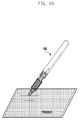
- FIG. 6 illustrates a palm rejection function using the position of the pen input device according to various embodiments of the present disclosure.
- the digitizer pad 350 senses the hovering of the pen input device 100, all the coordinates, which have been recognized by the electrostatic capacitive touch panel controller 330 until the hovering is separated, can be rejected, as illustrated in FIG. 6a .
- a write pressure of the pen input device 100 exists, as illustrated in FIG. 6b , in a case where a passive stylus coordinate within a designated distance from an EMR coordinate is separately recognizable, or when a touch coordinate is simultaneously recognized, it is used as the stylus coordinate and the EMR coordinate can be used so as to calculate the inclined direction and the inclined angle. At this time, the passive stylus coordinate and the touch coordinate out of the range can be rejected.
- the coordinate of the pen input device 100 can be recognized by the electrostatic capacitive touch panel 320, and the write pressure can be recognized by the digitizer pad 350.
- An output corresponding to the write pressure, which is recognized at the position of the coordinate of the recognized pen input device 100, can be output to the screen window 310.
- FIG. 7 is a schematic view for describing the measurement of the inclined angle and inclined direction of the pen input device according to various embodiments of the present disclosure.
- Equation 1 archcos ( ⁇ Xb - Xa 2 + Yb - Ya 2 / d
- T is an inclined angle
- a is an input coordinate input by touching by the tip 110 of the passive electrostatic stylus pen as the pen input device 100
- b is a recognition coordinate obtained by electromagnetic induction
- d is a distance between the tip 110 of the pen input device 100 and the coil center of the electromagnetic induction unit
- f indicates a write pressure of the pen input device 100.
- the distance d is changed depending on the write pressure f, and thus can be calculated through table conversion (or arithmetic operation).
- the processor 440 can calculate Equation 1 using the coordinate information provided by the electrostatic capacitive touch pad controller 330 and the digitizer pad controller 360, and then can generate inclination information (i.e. can calculate the inclined angle T) through arccosine table conversion (or arithmetic operation).
- the processor of the electronic device 500 is capable of calculating the unit vector V in the inclined direction by performing an arithmetic operation through Equation 2 using the coordinate information provided by the electrostatic capacitive touch pad controller 330 and the digitizer pad controller 360, and can perform coordinate correction to the unit vector V by calculating an azimuth through the conversion (or arithmetic operation) using the table stored in the internal memory 420.
- a pen input device is a hybrid stylus pen that uses a single coil supporting both of an EMR pen function and a passive electrostatic stylus (touch pen) function.
- a frequency change of a magnetic field which is generated by an electromagnetic induction method, is capable of being recognized by a single channel digitizer so as to recognize a write pressure of the pen input device, and based on this, an inclined angle and an inclined direction can be calculated and the error caused by the inclination can be improved.
- both the EMR pen function and the passive electrostatic stylus (touch pen) function can be supported using the single coil, and based on this, the inclined angle and the inclined direction can be calculated and the error caused by the inclination can be improved, there is an advantage in that more accurate coordinate information can be provided.
- the tip of the pen and the band-shaped portion on the housing grip portion are made of a dielectric material, charge mobility from a touch screen panel to a hand (ground) can be enhanced to improve an SNR (Signal to Noise Ratio), a more accurate electrostatic touch coordinate can be obtained without greatly increasing the area of the dielectric material, and the electrostatic touch coordinate obtained thereby can be used as a final input coordinate.
- SNR Signal to Noise Ratio
- an inclination error can be improved using a write pressure and an EMR coordinate regardless of an input direction, and an inclined angle and an inclined direction can be provided, more accurate coordinate information can be provided.
Landscapes
- Engineering & Computer Science (AREA)
- General Engineering & Computer Science (AREA)
- Theoretical Computer Science (AREA)
- Physics & Mathematics (AREA)
- Human Computer Interaction (AREA)
- General Physics & Mathematics (AREA)
- Electromagnetism (AREA)
- Position Input By Displaying (AREA)
Applications Claiming Priority (1)
| Application Number | Priority Date | Filing Date | Title |
|---|---|---|---|
| KR1020140168679A KR102307692B1 (ko) | 2014-11-28 | 2014-11-28 | 펜 입력장치, 그 입력 좌표 보정방법 및 이를 제공하는 전자장치 |
Publications (3)
| Publication Number | Publication Date |
|---|---|
| EP3035168A2 true EP3035168A2 (de) | 2016-06-22 |
| EP3035168A3 EP3035168A3 (de) | 2016-09-14 |
| EP3035168B1 EP3035168B1 (de) | 2020-07-08 |
Family
ID=54707608
Family Applications (1)
| Application Number | Title | Priority Date | Filing Date |
|---|---|---|---|
| EP15196498.8A Active EP3035168B1 (de) | 2014-11-28 | 2015-11-26 | Stifteingabevorrichtung, verfahren zur korrektur von eingabekoordinaten dafür und elektronische vorrichtung zur unterstützung davon |
Country Status (4)
| Country | Link |
|---|---|
| US (1) | US10095354B2 (de) |
| EP (1) | EP3035168B1 (de) |
| KR (1) | KR102307692B1 (de) |
| CN (1) | CN105653069B (de) |
Cited By (2)
| Publication number | Priority date | Publication date | Assignee | Title |
|---|---|---|---|---|
| CN109213381A (zh) * | 2018-11-19 | 2019-01-15 | 京东方科技集团股份有限公司 | 触控面板、触控显示面板和触控系统 |
| CN110010132A (zh) * | 2019-04-08 | 2019-07-12 | 安徽汇迈信息科技有限公司 | 一种集成语音的电子病历生产方法 |
Families Citing this family (36)
| Publication number | Priority date | Publication date | Assignee | Title |
|---|---|---|---|---|
| KR20160092360A (ko) * | 2015-01-27 | 2016-08-04 | 삼성전자주식회사 | 스타일러스 펜 및 터치 패널 |
| US10248247B2 (en) * | 2015-11-05 | 2019-04-02 | Egalax_Empia Technology Inc. | Tethered stylus, touch sensitive electronic device and system and method thereof |
| CN107153481B (zh) * | 2016-03-03 | 2021-03-02 | 禾瑞亚科技股份有限公司 | 用于校正触控笔所受的压力值的触控处理方法、装置与系统 |
| US10296089B2 (en) * | 2016-08-10 | 2019-05-21 | Microsoft Technology Licensing, Llc | Haptic stylus |
| WO2018032426A1 (zh) | 2016-08-17 | 2018-02-22 | 深圳市汇顶科技股份有限公司 | 检测输入设备的方法和检测设备 |
| US10310636B2 (en) * | 2016-11-04 | 2019-06-04 | Microsoft Technology Licensing, Llc | Active stylus |
| CN107111387B (zh) * | 2016-12-01 | 2020-06-23 | 深圳市汇顶科技股份有限公司 | 确定方位角或姿态的方法、触控输入装置、触控屏及系统 |
| US10635246B2 (en) * | 2017-03-10 | 2020-04-28 | Cypress Semiconductor Corporation | Capacitance sensing and inductance sensing in different modes |
| WO2018173420A1 (ja) * | 2017-03-24 | 2018-09-27 | 株式会社ワコム | 電子ペン |
| JP6359790B1 (ja) * | 2017-03-24 | 2018-07-18 | 株式会社ワコム | 電子ペン |
| CN107463288B (zh) * | 2017-05-26 | 2021-01-26 | 深圳市合众力拓科技有限公司 | 一种数字输入系统及实现方法 |
| US10444875B2 (en) * | 2017-05-30 | 2019-10-15 | Egalax_Empia Technology Inc. | Touch sensitive processing apparatus, method and system |
| CN110869897A (zh) * | 2017-07-14 | 2020-03-06 | 株式会社和冠 | 修正笔坐标与指示器的显示位置之间的偏离的方法 |
| JP6902423B2 (ja) * | 2017-07-31 | 2021-07-14 | シャープ株式会社 | 筆記入力システム、ボードおよび識別子 |
| TWI630513B (zh) * | 2017-08-04 | 2018-07-21 | Waltop International Corporation | 可提供傾斜角與方位角偵測訊號的電容筆 |
| KR102054960B1 (ko) * | 2017-12-08 | 2019-12-12 | 주식회사 하이딥 | 스타일러스 펜 및 그 제조 방법 |
| WO2019113906A1 (zh) * | 2017-12-14 | 2019-06-20 | 深圳市汇顶科技股份有限公司 | 触控笔的坐标确定方法、装置、电子设备及存储介质 |
| KR20190074335A (ko) * | 2017-12-19 | 2019-06-28 | 삼성디스플레이 주식회사 | 스타일러스를 포함하는 전자장치 및 이의 동작방법 |
| CN109947272B (zh) * | 2019-03-25 | 2020-04-14 | 京东方科技集团股份有限公司 | 触控笔及驱动方法 |
| WO2020066160A1 (ja) | 2018-09-27 | 2020-04-02 | 株式会社ワコム | 座標検出方法 |
| CN112346582B (zh) * | 2019-08-08 | 2022-07-22 | 华为技术有限公司 | 一种触控笔以及电子设备 |
| WO2021200521A1 (ja) * | 2020-03-31 | 2021-10-07 | 株式会社ワコム | ノック式電子ペン |
| CN111380650B (zh) * | 2020-06-01 | 2020-09-18 | 深圳市千分一智能技术有限公司 | 压力曲线校准方法、装置、设备及可读存储介质 |
| JP7688648B2 (ja) | 2020-09-04 | 2025-06-04 | 株式会社ワコム | 位置指示器 |
| CN112148139B (zh) * | 2020-09-28 | 2022-07-26 | 联想(北京)有限公司 | 一种姿态识别方法和计算机可读存储介质 |
| JP7506582B2 (ja) * | 2020-11-02 | 2024-06-26 | 三菱鉛筆株式会社 | 入力ペン |
| US11803257B2 (en) * | 2020-11-02 | 2023-10-31 | Japan Display Inc. | Input support device and input detection system |
| KR102519345B1 (ko) * | 2020-12-22 | 2023-04-10 | 유현우 | 오브젝트의 위치 및 종류 식별 장치 |
| CN112711341B (zh) * | 2021-01-05 | 2023-06-20 | 北京字节跳动网络技术有限公司 | 书写装置的控制方法、装置、终端和存储介质 |
| CN113178900B (zh) * | 2021-03-15 | 2023-02-17 | 荣耀终端有限公司 | 无线充电系统、芯片和无线充电电路 |
| CN113111312B (zh) * | 2021-04-13 | 2023-09-26 | 深圳市绘王动漫科技有限公司 | 方位角及旋转角的侦测方法及手写装置 |
| CN118140200A (zh) * | 2021-10-21 | 2024-06-04 | 希迪普公司 | 笔及触摸输入系统 |
| KR20250060937A (ko) * | 2021-10-21 | 2025-05-07 | 주식회사 하이딥 | 펜 및 터치 입력 시스템 |
| JP7569577B2 (ja) * | 2022-06-16 | 2024-10-18 | 株式会社 ハイディープ | ペン及びタッチ入力システム及びコントローラ |
| CN114816139B (zh) * | 2022-06-24 | 2022-11-01 | 基合半导体(宁波)有限公司 | 一种电容屏、电容屏与触控笔的交互方法及存储介质 |
| KR20240014658A (ko) | 2022-07-25 | 2024-02-02 | 삼성디스플레이 주식회사 | 표시 장치 |
Family Cites Families (18)
| Publication number | Priority date | Publication date | Assignee | Title |
|---|---|---|---|---|
| US6259438B1 (en) * | 1998-06-04 | 2001-07-10 | Wacom Co., Ltd. | Coordinate input stylus |
| JPH09230989A (ja) | 1996-02-26 | 1997-09-05 | Graphtec Corp | デジタイザ |
| US6552538B2 (en) * | 2001-04-11 | 2003-04-22 | Koninklijke Philips Electronics, N.V. | RF transmit calibration for open MRI systems |
| US7310091B2 (en) * | 2003-09-16 | 2007-12-18 | Acer Incorporated | Handwriting pen capable of simulating different strokes |
| US20110162894A1 (en) * | 2010-01-06 | 2011-07-07 | Apple Inc. | Stylus for touch sensing devices |
| US8482539B2 (en) * | 2010-01-12 | 2013-07-09 | Panasonic Corporation | Electronic pen system |
| KR200462280Y1 (ko) | 2010-02-08 | 2012-09-04 | 이승희 | 정전용량방식의 터치스크린을 갖는 휴대용 단말기에 적용되는 정전용량방식의 터치펜 겸용 필기구 |
| US9864440B2 (en) * | 2010-06-11 | 2018-01-09 | Microsoft Technology Licensing, Llc | Object orientation detection with a digitizer |
| JP5892595B2 (ja) * | 2012-02-06 | 2016-03-23 | 株式会社ワコム | 位置指示器 |
| KR101988310B1 (ko) * | 2012-10-31 | 2019-06-12 | 엘지전자 주식회사 | 정전식 스타일러스 펜 및 이를 포함하는 이동 단말기 |
| US9442578B2 (en) * | 2012-08-06 | 2016-09-13 | Lg Electronics Inc. | Capacitive type stylus and mobile terminal comprising the same |
| KR101995403B1 (ko) * | 2012-09-14 | 2019-07-02 | 삼성전자 주식회사 | 스타일러스 펜, 이를 이용한 입력 처리 방법 및 그 전자 장치 |
| JP6080256B2 (ja) * | 2012-12-17 | 2017-02-15 | 株式会社ワコム | 静電方式スタイラスペン |
| JP2014139759A (ja) * | 2013-01-21 | 2014-07-31 | Toshiba Corp | 情報機器及び情報処理方法 |
| US20140204038A1 (en) * | 2013-01-21 | 2014-07-24 | Kabushiki Kaisha Toshiba | Information apparatus and information processing method |
| US20140247238A1 (en) * | 2013-03-01 | 2014-09-04 | Barnesandnoble.Com Llc | System and method for dual mode stylus detection |
| TWM470283U (zh) * | 2013-06-19 | 2014-01-11 | Waltop Int Corp | 觸控輸入裝置 |
| US9513721B2 (en) * | 2013-09-12 | 2016-12-06 | Microsoft Technology Licensing, Llc | Pressure sensitive stylus for a digitizer |
-
2014
- 2014-11-28 KR KR1020140168679A patent/KR102307692B1/ko active Active
-
2015
- 2015-11-26 EP EP15196498.8A patent/EP3035168B1/de active Active
- 2015-11-27 CN CN201510848587.6A patent/CN105653069B/zh active Active
- 2015-11-27 US US14/953,237 patent/US10095354B2/en active Active
Non-Patent Citations (1)
| Title |
|---|
| None |
Cited By (2)
| Publication number | Priority date | Publication date | Assignee | Title |
|---|---|---|---|---|
| CN109213381A (zh) * | 2018-11-19 | 2019-01-15 | 京东方科技集团股份有限公司 | 触控面板、触控显示面板和触控系统 |
| CN110010132A (zh) * | 2019-04-08 | 2019-07-12 | 安徽汇迈信息科技有限公司 | 一种集成语音的电子病历生产方法 |
Also Published As
| Publication number | Publication date |
|---|---|
| EP3035168B1 (de) | 2020-07-08 |
| KR102307692B1 (ko) | 2021-10-05 |
| KR20160064719A (ko) | 2016-06-08 |
| CN105653069A (zh) | 2016-06-08 |
| CN105653069B (zh) | 2020-07-21 |
| US20160154528A1 (en) | 2016-06-02 |
| US10095354B2 (en) | 2018-10-09 |
| EP3035168A3 (de) | 2016-09-14 |
Similar Documents
| Publication | Publication Date | Title |
|---|---|---|
| US10095354B2 (en) | Pen input device, method for correcting input coordinate thereof and electronic device for supporting the same | |
| US9977529B2 (en) | Method for switching digitizer mode | |
| CN107577361B (zh) | 坐标测量装置和识别接触物体的位置的方法 | |
| CN104516549B (zh) | 触摸感测系统及其驱动方法 | |
| EP2711825B1 (de) | System zur Bereitstellung einer Benutzerschnittstelle zur Verwendung durch tragbare und andere Vorrichtungen | |
| CN103984424B (zh) | 电子笔、识别电子笔的电子装置和操作电子装置的方法 | |
| CN103389804B (zh) | 坐标指示设备和用于测量其输入位置的坐标测量设备 | |
| US10037111B2 (en) | Single point charger | |
| CN105706020A (zh) | 用于电子装置或计算机装置的保护附件设备和配备有这种附件设备的装置 | |
| JPWO2015182222A1 (ja) | 指示体検出装置及びその信号処理方法 | |
| US9760277B2 (en) | Electronic device and method for detecting proximity input and touch input | |
| KR102253676B1 (ko) | 터치 센싱 시스템과 그 구동 방법 | |
| US10120466B2 (en) | Pen input device having malfunction prevention function and method of preventing malfunction thereof | |
| KR20140137629A (ko) | 이어폰 연결을 감지하는 휴대 단말 및 방법 | |
| US20150035764A1 (en) | Digitizer pen | |
| US9519386B2 (en) | Input device and electronic device including the same | |
| KR102234249B1 (ko) | 터치 스크린 장치와 이의 엣지 좌표 보상방법 | |
| EP4191828A1 (de) | Elektronische vorrichtung mit fähigkeit zum drahtlosen laden |
Legal Events
| Date | Code | Title | Description |
|---|---|---|---|
| PUAI | Public reference made under article 153(3) epc to a published international application that has entered the european phase |
Free format text: ORIGINAL CODE: 0009012 |
|
| AK | Designated contracting states |
Kind code of ref document: A2 Designated state(s): AL AT BE BG CH CY CZ DE DK EE ES FI FR GB GR HR HU IE IS IT LI LT LU LV MC MK MT NL NO PL PT RO RS SE SI SK SM TR |
|
| AX | Request for extension of the european patent |
Extension state: BA ME |
|
| PUAL | Search report despatched |
Free format text: ORIGINAL CODE: 0009013 |
|
| AK | Designated contracting states |
Kind code of ref document: A3 Designated state(s): AL AT BE BG CH CY CZ DE DK EE ES FI FR GB GR HR HU IE IS IT LI LT LU LV MC MK MT NL NO PL PT RO RS SE SI SK SM TR |
|
| AX | Request for extension of the european patent |
Extension state: BA ME |
|
| RIC1 | Information provided on ipc code assigned before grant |
Ipc: G06F 3/0354 20130101ALI20160811BHEP Ipc: G06F 3/038 20130101AFI20160811BHEP Ipc: G06F 3/046 20060101ALI20160811BHEP Ipc: G06F 3/044 20060101ALI20160811BHEP |
|
| STAA | Information on the status of an ep patent application or granted ep patent |
Free format text: STATUS: REQUEST FOR EXAMINATION WAS MADE |
|
| 17P | Request for examination filed |
Effective date: 20161215 |
|
| RBV | Designated contracting states (corrected) |
Designated state(s): AL AT BE BG CH CY CZ DE DK EE ES FI FR GB GR HR HU IE IS IT LI LT LU LV MC MK MT NL NO PL PT RO RS SE SI SK SM TR |
|
| GRAP | Despatch of communication of intention to grant a patent |
Free format text: ORIGINAL CODE: EPIDOSNIGR1 |
|
| STAA | Information on the status of an ep patent application or granted ep patent |
Free format text: STATUS: GRANT OF PATENT IS INTENDED |
|
| RIC1 | Information provided on ipc code assigned before grant |
Ipc: G06F 3/046 20060101ALI20170301BHEP Ipc: G06F 3/038 20130101AFI20170301BHEP Ipc: G06F 3/044 20060101ALI20170301BHEP Ipc: G06F 3/041 20060101ALI20170301BHEP Ipc: G06F 3/0354 20130101ALI20170301BHEP |
|
| INTG | Intention to grant announced |
Effective date: 20170330 |
|
| GRAJ | Information related to disapproval of communication of intention to grant by the applicant or resumption of examination proceedings by the epo deleted |
Free format text: ORIGINAL CODE: EPIDOSDIGR1 |
|
| STAA | Information on the status of an ep patent application or granted ep patent |
Free format text: STATUS: REQUEST FOR EXAMINATION WAS MADE |
|
| STAA | Information on the status of an ep patent application or granted ep patent |
Free format text: STATUS: EXAMINATION IS IN PROGRESS |
|
| INTC | Intention to grant announced (deleted) | ||
| 17Q | First examination report despatched |
Effective date: 20170908 |
|
| GRAP | Despatch of communication of intention to grant a patent |
Free format text: ORIGINAL CODE: EPIDOSNIGR1 |
|
| STAA | Information on the status of an ep patent application or granted ep patent |
Free format text: STATUS: GRANT OF PATENT IS INTENDED |
|
| INTG | Intention to grant announced |
Effective date: 20200205 |
|
| GRAS | Grant fee paid |
Free format text: ORIGINAL CODE: EPIDOSNIGR3 |
|
| GRAA | (expected) grant |
Free format text: ORIGINAL CODE: 0009210 |
|
| STAA | Information on the status of an ep patent application or granted ep patent |
Free format text: STATUS: THE PATENT HAS BEEN GRANTED |
|
| AK | Designated contracting states |
Kind code of ref document: B1 Designated state(s): AL AT BE BG CH CY CZ DE DK EE ES FI FR GB GR HR HU IE IS IT LI LT LU LV MC MK MT NL NO PL PT RO RS SE SI SK SM TR |
|
| REG | Reference to a national code |
Ref country code: CH Ref legal event code: EP Ref country code: AT Ref legal event code: REF Ref document number: 1289151 Country of ref document: AT Kind code of ref document: T Effective date: 20200715 |
|
| REG | Reference to a national code |
Ref country code: DE Ref legal event code: R096 Ref document number: 602015055340 Country of ref document: DE |
|
| REG | Reference to a national code |
Ref country code: IE Ref legal event code: FG4D |
|
| REG | Reference to a national code |
Ref country code: NL Ref legal event code: FP |
|
| REG | Reference to a national code |
Ref country code: LT Ref legal event code: MG4D |
|
| REG | Reference to a national code |
Ref country code: AT Ref legal event code: MK05 Ref document number: 1289151 Country of ref document: AT Kind code of ref document: T Effective date: 20200708 |
|
| PG25 | Lapsed in a contracting state [announced via postgrant information from national office to epo] |
Ref country code: NO Free format text: LAPSE BECAUSE OF FAILURE TO SUBMIT A TRANSLATION OF THE DESCRIPTION OR TO PAY THE FEE WITHIN THE PRESCRIBED TIME-LIMIT Effective date: 20201008 Ref country code: GR Free format text: LAPSE BECAUSE OF FAILURE TO SUBMIT A TRANSLATION OF THE DESCRIPTION OR TO PAY THE FEE WITHIN THE PRESCRIBED TIME-LIMIT Effective date: 20201009 Ref country code: SE Free format text: LAPSE BECAUSE OF FAILURE TO SUBMIT A TRANSLATION OF THE DESCRIPTION OR TO PAY THE FEE WITHIN THE PRESCRIBED TIME-LIMIT Effective date: 20200708 Ref country code: FI Free format text: LAPSE BECAUSE OF FAILURE TO SUBMIT A TRANSLATION OF THE DESCRIPTION OR TO PAY THE FEE WITHIN THE PRESCRIBED TIME-LIMIT Effective date: 20200708 Ref country code: LT Free format text: LAPSE BECAUSE OF FAILURE TO SUBMIT A TRANSLATION OF THE DESCRIPTION OR TO PAY THE FEE WITHIN THE PRESCRIBED TIME-LIMIT Effective date: 20200708 Ref country code: HR Free format text: LAPSE BECAUSE OF FAILURE TO SUBMIT A TRANSLATION OF THE DESCRIPTION OR TO PAY THE FEE WITHIN THE PRESCRIBED TIME-LIMIT Effective date: 20200708 Ref country code: AT Free format text: LAPSE BECAUSE OF FAILURE TO SUBMIT A TRANSLATION OF THE DESCRIPTION OR TO PAY THE FEE WITHIN THE PRESCRIBED TIME-LIMIT Effective date: 20200708 Ref country code: ES Free format text: LAPSE BECAUSE OF FAILURE TO SUBMIT A TRANSLATION OF THE DESCRIPTION OR TO PAY THE FEE WITHIN THE PRESCRIBED TIME-LIMIT Effective date: 20200708 Ref country code: BG Free format text: LAPSE BECAUSE OF FAILURE TO SUBMIT A TRANSLATION OF THE DESCRIPTION OR TO PAY THE FEE WITHIN THE PRESCRIBED TIME-LIMIT Effective date: 20201008 Ref country code: PT Free format text: LAPSE BECAUSE OF FAILURE TO SUBMIT A TRANSLATION OF THE DESCRIPTION OR TO PAY THE FEE WITHIN THE PRESCRIBED TIME-LIMIT Effective date: 20201109 |
|
| PG25 | Lapsed in a contracting state [announced via postgrant information from national office to epo] |
Ref country code: PL Free format text: LAPSE BECAUSE OF FAILURE TO SUBMIT A TRANSLATION OF THE DESCRIPTION OR TO PAY THE FEE WITHIN THE PRESCRIBED TIME-LIMIT Effective date: 20200708 Ref country code: LV Free format text: LAPSE BECAUSE OF FAILURE TO SUBMIT A TRANSLATION OF THE DESCRIPTION OR TO PAY THE FEE WITHIN THE PRESCRIBED TIME-LIMIT Effective date: 20200708 Ref country code: RS Free format text: LAPSE BECAUSE OF FAILURE TO SUBMIT A TRANSLATION OF THE DESCRIPTION OR TO PAY THE FEE WITHIN THE PRESCRIBED TIME-LIMIT Effective date: 20200708 Ref country code: IS Free format text: LAPSE BECAUSE OF FAILURE TO SUBMIT A TRANSLATION OF THE DESCRIPTION OR TO PAY THE FEE WITHIN THE PRESCRIBED TIME-LIMIT Effective date: 20201108 |
|
| REG | Reference to a national code |
Ref country code: DE Ref legal event code: R097 Ref document number: 602015055340 Country of ref document: DE |
|
| PG25 | Lapsed in a contracting state [announced via postgrant information from national office to epo] |
Ref country code: RO Free format text: LAPSE BECAUSE OF FAILURE TO SUBMIT A TRANSLATION OF THE DESCRIPTION OR TO PAY THE FEE WITHIN THE PRESCRIBED TIME-LIMIT Effective date: 20200708 Ref country code: SM Free format text: LAPSE BECAUSE OF FAILURE TO SUBMIT A TRANSLATION OF THE DESCRIPTION OR TO PAY THE FEE WITHIN THE PRESCRIBED TIME-LIMIT Effective date: 20200708 Ref country code: EE Free format text: LAPSE BECAUSE OF FAILURE TO SUBMIT A TRANSLATION OF THE DESCRIPTION OR TO PAY THE FEE WITHIN THE PRESCRIBED TIME-LIMIT Effective date: 20200708 Ref country code: IT Free format text: LAPSE BECAUSE OF FAILURE TO SUBMIT A TRANSLATION OF THE DESCRIPTION OR TO PAY THE FEE WITHIN THE PRESCRIBED TIME-LIMIT Effective date: 20200708 Ref country code: DK Free format text: LAPSE BECAUSE OF FAILURE TO SUBMIT A TRANSLATION OF THE DESCRIPTION OR TO PAY THE FEE WITHIN THE PRESCRIBED TIME-LIMIT Effective date: 20200708 Ref country code: CZ Free format text: LAPSE BECAUSE OF FAILURE TO SUBMIT A TRANSLATION OF THE DESCRIPTION OR TO PAY THE FEE WITHIN THE PRESCRIBED TIME-LIMIT Effective date: 20200708 |
|
| PLBE | No opposition filed within time limit |
Free format text: ORIGINAL CODE: 0009261 |
|
| STAA | Information on the status of an ep patent application or granted ep patent |
Free format text: STATUS: NO OPPOSITION FILED WITHIN TIME LIMIT |
|
| PG25 | Lapsed in a contracting state [announced via postgrant information from national office to epo] |
Ref country code: AL Free format text: LAPSE BECAUSE OF FAILURE TO SUBMIT A TRANSLATION OF THE DESCRIPTION OR TO PAY THE FEE WITHIN THE PRESCRIBED TIME-LIMIT Effective date: 20200708 |
|
| 26N | No opposition filed |
Effective date: 20210409 |
|
| PG25 | Lapsed in a contracting state [announced via postgrant information from national office to epo] |
Ref country code: MC Free format text: LAPSE BECAUSE OF FAILURE TO SUBMIT A TRANSLATION OF THE DESCRIPTION OR TO PAY THE FEE WITHIN THE PRESCRIBED TIME-LIMIT Effective date: 20200708 Ref country code: SK Free format text: LAPSE BECAUSE OF FAILURE TO SUBMIT A TRANSLATION OF THE DESCRIPTION OR TO PAY THE FEE WITHIN THE PRESCRIBED TIME-LIMIT Effective date: 20200708 |
|
| REG | Reference to a national code |
Ref country code: CH Ref legal event code: PL |
|
| PG25 | Lapsed in a contracting state [announced via postgrant information from national office to epo] |
Ref country code: LU Free format text: LAPSE BECAUSE OF NON-PAYMENT OF DUE FEES Effective date: 20201126 |
|
| REG | Reference to a national code |
Ref country code: BE Ref legal event code: MM Effective date: 20201130 |
|
| PG25 | Lapsed in a contracting state [announced via postgrant information from national office to epo] |
Ref country code: CH Free format text: LAPSE BECAUSE OF NON-PAYMENT OF DUE FEES Effective date: 20201130 Ref country code: LI Free format text: LAPSE BECAUSE OF NON-PAYMENT OF DUE FEES Effective date: 20201130 Ref country code: SI Free format text: LAPSE BECAUSE OF FAILURE TO SUBMIT A TRANSLATION OF THE DESCRIPTION OR TO PAY THE FEE WITHIN THE PRESCRIBED TIME-LIMIT Effective date: 20200708 |
|
| PG25 | Lapsed in a contracting state [announced via postgrant information from national office to epo] |
Ref country code: FR Free format text: LAPSE BECAUSE OF NON-PAYMENT OF DUE FEES Effective date: 20201130 Ref country code: IE Free format text: LAPSE BECAUSE OF NON-PAYMENT OF DUE FEES Effective date: 20201126 |
|
| PG25 | Lapsed in a contracting state [announced via postgrant information from national office to epo] |
Ref country code: TR Free format text: LAPSE BECAUSE OF FAILURE TO SUBMIT A TRANSLATION OF THE DESCRIPTION OR TO PAY THE FEE WITHIN THE PRESCRIBED TIME-LIMIT Effective date: 20200708 Ref country code: MT Free format text: LAPSE BECAUSE OF FAILURE TO SUBMIT A TRANSLATION OF THE DESCRIPTION OR TO PAY THE FEE WITHIN THE PRESCRIBED TIME-LIMIT Effective date: 20200708 Ref country code: CY Free format text: LAPSE BECAUSE OF FAILURE TO SUBMIT A TRANSLATION OF THE DESCRIPTION OR TO PAY THE FEE WITHIN THE PRESCRIBED TIME-LIMIT Effective date: 20200708 |
|
| PG25 | Lapsed in a contracting state [announced via postgrant information from national office to epo] |
Ref country code: MK Free format text: LAPSE BECAUSE OF FAILURE TO SUBMIT A TRANSLATION OF THE DESCRIPTION OR TO PAY THE FEE WITHIN THE PRESCRIBED TIME-LIMIT Effective date: 20200708 |
|
| PG25 | Lapsed in a contracting state [announced via postgrant information from national office to epo] |
Ref country code: BE Free format text: LAPSE BECAUSE OF NON-PAYMENT OF DUE FEES Effective date: 20201130 |
|
| PGFP | Annual fee paid to national office [announced via postgrant information from national office to epo] |
Ref country code: NL Payment date: 20251002 Year of fee payment: 11 |
|
| PGFP | Annual fee paid to national office [announced via postgrant information from national office to epo] |
Ref country code: DE Payment date: 20251002 Year of fee payment: 11 |
|
| PGFP | Annual fee paid to national office [announced via postgrant information from national office to epo] |
Ref country code: GB Payment date: 20251001 Year of fee payment: 11 |