EP3035404A1 - Barrierenfolie mit elektrischem Stromkreis - Google Patents
Barrierenfolie mit elektrischem Stromkreis Download PDFInfo
- Publication number
- EP3035404A1 EP3035404A1 EP14198191.0A EP14198191A EP3035404A1 EP 3035404 A1 EP3035404 A1 EP 3035404A1 EP 14198191 A EP14198191 A EP 14198191A EP 3035404 A1 EP3035404 A1 EP 3035404A1
- Authority
- EP
- European Patent Office
- Prior art keywords
- foil
- barrier
- groove
- barrier foil
- sealing material
- Prior art date
- Legal status (The legal status is an assumption and is not a legal conclusion. Google has not performed a legal analysis and makes no representation as to the accuracy of the status listed.)
- Withdrawn
Links
- 239000011888 foil Substances 0.000 title claims abstract description 316
- 230000004888 barrier function Effects 0.000 title claims abstract description 283
- 239000010410 layer Substances 0.000 claims abstract description 166
- 239000003566 sealing material Substances 0.000 claims abstract description 73
- 239000012044 organic layer Substances 0.000 claims abstract description 64
- 238000000034 method Methods 0.000 claims abstract description 59
- QVGXLLKOCUKJST-UHFFFAOYSA-N atomic oxygen Chemical compound [O] QVGXLLKOCUKJST-UHFFFAOYSA-N 0.000 claims abstract description 42
- 239000011368 organic material Substances 0.000 claims abstract description 39
- 239000001301 oxygen Substances 0.000 claims abstract description 35
- 229910052760 oxygen Inorganic materials 0.000 claims abstract description 35
- 239000004020 conductor Substances 0.000 claims abstract description 13
- 238000005520 cutting process Methods 0.000 claims description 61
- 238000000151 deposition Methods 0.000 claims description 56
- 239000000758 substrate Substances 0.000 claims description 40
- 239000000463 material Substances 0.000 claims description 29
- 238000007789 sealing Methods 0.000 claims description 29
- 230000008021 deposition Effects 0.000 claims description 28
- 229910000679 solder Inorganic materials 0.000 claims description 19
- 238000009736 wetting Methods 0.000 claims description 11
- 230000008901 benefit Effects 0.000 description 14
- 230000008569 process Effects 0.000 description 14
- 230000007613 environmental effect Effects 0.000 description 12
- 238000004519 manufacturing process Methods 0.000 description 12
- 230000006870 function Effects 0.000 description 7
- QVGXLLKOCUKJST-AKLPVKDBSA-N oxygen-19 atom Chemical compound [19O] QVGXLLKOCUKJST-AKLPVKDBSA-N 0.000 description 7
- 238000012545 processing Methods 0.000 description 7
- 230000006378 damage Effects 0.000 description 6
- 230000005540 biological transmission Effects 0.000 description 5
- 238000013461 design Methods 0.000 description 5
- 238000013459 approach Methods 0.000 description 4
- 230000015572 biosynthetic process Effects 0.000 description 4
- 239000011248 coating agent Substances 0.000 description 4
- 238000000576 coating method Methods 0.000 description 4
- 229910052751 metal Inorganic materials 0.000 description 4
- 239000002184 metal Substances 0.000 description 4
- XLYOFNOQVPJJNP-UHFFFAOYSA-N water Chemical compound O XLYOFNOQVPJJNP-UHFFFAOYSA-N 0.000 description 4
- BQCADISMDOOEFD-UHFFFAOYSA-N Silver Chemical compound [Ag] BQCADISMDOOEFD-UHFFFAOYSA-N 0.000 description 3
- 238000005538 encapsulation Methods 0.000 description 3
- 150000002739 metals Chemical class 0.000 description 3
- 238000000059 patterning Methods 0.000 description 3
- 229910052709 silver Inorganic materials 0.000 description 3
- 239000004332 silver Substances 0.000 description 3
- IJGRMHOSHXDMSA-UHFFFAOYSA-N Atomic nitrogen Chemical compound N#N IJGRMHOSHXDMSA-UHFFFAOYSA-N 0.000 description 2
- 239000004696 Poly ether ether ketone Substances 0.000 description 2
- 230000009286 beneficial effect Effects 0.000 description 2
- 230000006866 deterioration Effects 0.000 description 2
- 230000002542 deteriorative effect Effects 0.000 description 2
- 230000000694 effects Effects 0.000 description 2
- 230000008018 melting Effects 0.000 description 2
- 238000002844 melting Methods 0.000 description 2
- 150000004767 nitrides Chemical class 0.000 description 2
- 230000003287 optical effect Effects 0.000 description 2
- 238000013086 organic photovoltaic Methods 0.000 description 2
- 238000000623 plasma-assisted chemical vapour deposition Methods 0.000 description 2
- 229920002530 polyetherether ketone Polymers 0.000 description 2
- -1 polyethylene terephthalate Polymers 0.000 description 2
- 229920000139 polyethylene terephthalate Polymers 0.000 description 2
- 239000005020 polyethylene terephthalate Substances 0.000 description 2
- 238000012546 transfer Methods 0.000 description 2
- NIXOWILDQLNWCW-UHFFFAOYSA-M Acrylate Chemical compound [O-]C(=O)C=C NIXOWILDQLNWCW-UHFFFAOYSA-M 0.000 description 1
- 235000001674 Agaricus brunnescens Nutrition 0.000 description 1
- RYGMFSIKBFXOCR-UHFFFAOYSA-N Copper Chemical compound [Cu] RYGMFSIKBFXOCR-UHFFFAOYSA-N 0.000 description 1
- GYHNNYVSQQEPJS-UHFFFAOYSA-N Gallium Chemical compound [Ga] GYHNNYVSQQEPJS-UHFFFAOYSA-N 0.000 description 1
- 239000004698 Polyethylene Substances 0.000 description 1
- 229910052581 Si3N4 Inorganic materials 0.000 description 1
- ATJFFYVFTNAWJD-UHFFFAOYSA-N Tin Chemical compound [Sn] ATJFFYVFTNAWJD-UHFFFAOYSA-N 0.000 description 1
- HCHKCACWOHOZIP-UHFFFAOYSA-N Zinc Chemical compound [Zn] HCHKCACWOHOZIP-UHFFFAOYSA-N 0.000 description 1
- 238000004026 adhesive bonding Methods 0.000 description 1
- 230000002411 adverse Effects 0.000 description 1
- 229910052787 antimony Inorganic materials 0.000 description 1
- WATWJIUSRGPENY-UHFFFAOYSA-N antimony atom Chemical compound [Sb] WATWJIUSRGPENY-UHFFFAOYSA-N 0.000 description 1
- 238000000149 argon plasma sintering Methods 0.000 description 1
- 229910052797 bismuth Inorganic materials 0.000 description 1
- JCXGWMGPZLAOME-UHFFFAOYSA-N bismuth atom Chemical compound [Bi] JCXGWMGPZLAOME-UHFFFAOYSA-N 0.000 description 1
- 238000010924 continuous production Methods 0.000 description 1
- 229910052802 copper Inorganic materials 0.000 description 1
- 239000010949 copper Substances 0.000 description 1
- HVMJUDPAXRRVQO-UHFFFAOYSA-N copper indium Chemical compound [Cu].[In] HVMJUDPAXRRVQO-UHFFFAOYSA-N 0.000 description 1
- 230000007547 defect Effects 0.000 description 1
- 230000000593 degrading effect Effects 0.000 description 1
- 230000001934 delay Effects 0.000 description 1
- 238000005137 deposition process Methods 0.000 description 1
- 238000009826 distribution Methods 0.000 description 1
- 230000005611 electricity Effects 0.000 description 1
- 229910052733 gallium Inorganic materials 0.000 description 1
- 239000011521 glass Substances 0.000 description 1
- 238000010438 heat treatment Methods 0.000 description 1
- 229910052738 indium Inorganic materials 0.000 description 1
- APFVFJFRJDLVQX-UHFFFAOYSA-N indium atom Chemical compound [In] APFVFJFRJDLVQX-UHFFFAOYSA-N 0.000 description 1
- 238000002347 injection Methods 0.000 description 1
- 239000007924 injection Substances 0.000 description 1
- 238000007641 inkjet printing Methods 0.000 description 1
- 229910010272 inorganic material Inorganic materials 0.000 description 1
- 239000011147 inorganic material Substances 0.000 description 1
- 238000002955 isolation Methods 0.000 description 1
- 238000010030 laminating Methods 0.000 description 1
- 239000011133 lead Substances 0.000 description 1
- 229910001092 metal group alloy Inorganic materials 0.000 description 1
- 229910052757 nitrogen Inorganic materials 0.000 description 1
- 230000000149 penetrating effect Effects 0.000 description 1
- 239000004417 polycarbonate Substances 0.000 description 1
- 229920000515 polycarbonate Polymers 0.000 description 1
- 229920000573 polyethylene Polymers 0.000 description 1
- 230000002265 prevention Effects 0.000 description 1
- 238000007639 printing Methods 0.000 description 1
- 150000003346 selenoethers Chemical class 0.000 description 1
- HQVNEWCFYHHQES-UHFFFAOYSA-N silicon nitride Chemical compound N12[Si]34N5[Si]62N3[Si]51N64 HQVNEWCFYHHQES-UHFFFAOYSA-N 0.000 description 1
- 239000000126 substance Substances 0.000 description 1
- 230000002195 synergetic effect Effects 0.000 description 1
- 230000003685 thermal hair damage Effects 0.000 description 1
- YFNCATAIYKQPOO-UHFFFAOYSA-N thiophanate Chemical compound CCOC(=O)NC(=S)NC1=CC=CC=C1NC(=S)NC(=O)OCC YFNCATAIYKQPOO-UHFFFAOYSA-N 0.000 description 1
- 239000011135 tin Substances 0.000 description 1
- 238000013519 translation Methods 0.000 description 1
- 238000011282 treatment Methods 0.000 description 1
- 239000002699 waste material Substances 0.000 description 1
- 229910052725 zinc Inorganic materials 0.000 description 1
- 239000011701 zinc Substances 0.000 description 1
Images


Classifications
-
- H—ELECTRICITY
- H10—SEMICONDUCTOR DEVICES; ELECTRIC SOLID-STATE DEVICES NOT OTHERWISE PROVIDED FOR
- H10K—ORGANIC ELECTRIC SOLID-STATE DEVICES
- H10K50/00—Organic light-emitting devices
- H10K50/80—Constructional details
- H10K50/84—Passivation; Containers; Encapsulations
- H10K50/844—Encapsulations
- H10K50/8445—Encapsulations multilayered coatings having a repetitive structure, e.g. having multiple organic-inorganic bilayers
-
- H—ELECTRICITY
- H10—SEMICONDUCTOR DEVICES; ELECTRIC SOLID-STATE DEVICES NOT OTHERWISE PROVIDED FOR
- H10K—ORGANIC ELECTRIC SOLID-STATE DEVICES
- H10K50/00—Organic light-emitting devices
- H10K50/80—Constructional details
- H10K50/84—Passivation; Containers; Encapsulations
- H10K50/842—Containers
- H10K50/8423—Metallic sealing arrangements
-
- H—ELECTRICITY
- H10—SEMICONDUCTOR DEVICES; ELECTRIC SOLID-STATE DEVICES NOT OTHERWISE PROVIDED FOR
- H10K—ORGANIC ELECTRIC SOLID-STATE DEVICES
- H10K50/00—Organic light-emitting devices
- H10K50/80—Constructional details
- H10K50/88—Terminals, e.g. bond pads
-
- H—ELECTRICITY
- H10—SEMICONDUCTOR DEVICES; ELECTRIC SOLID-STATE DEVICES NOT OTHERWISE PROVIDED FOR
- H10K—ORGANIC ELECTRIC SOLID-STATE DEVICES
- H10K71/00—Manufacture or treatment specially adapted for the organic devices covered by this subclass
- H10K71/851—Division of substrate
Definitions
- the present disclosure relates to a barrier foil comprising an electrical circuit, and a method and system for providing the same.
- Barrier foils find application in the production of device stacks for protecting sensitive components or materials from environmental influences.
- a device structure is sandwiched between barrier foils to prevent moisture and/or oxygen from seeping into the device structure.
- the device structure may e.g. comprise one or more organic layers forming an organic light emitting device (OLED), organic photovoltaic device (OPV), or other moisture and/or oxygen sensitive component.
- OLED organic light emitting device
- OOV organic photovoltaic device
- Large batches of device stacks may conveniently be produced in a roll-to-roll (R2R) or roll-to-sheet (R2S) process.
- R2R roll-to-roll
- R2S roll-to-sheet
- Such a process typically involves providing a continuous substrate known as a 'web' and passing this substrate through various production processes, e.g. involving deposition of various material layers on the substrate.
- a substrate may form a continuous barrier foil comprising a continuous layered structure with an organic layer sandwiched between barrier foil
- a busbar is an electrically conducting structure or circuit, e.g. strip or bar, comprising a material with relatively high conductivity to facilitate a substantial current throughput in an electrical circuit. To achieve high current, it is also desired to provide the busbar with a relatively large cross-section.
- a busbar is electrically connected to a circuit electrode to improve electrical access and/or conductivity to the electrode.
- the electrode may e.g. comprise a device layer having relatively low conductivity.
- the busbar can be in direct contact with the electrode, or connected via a shunt (short circuit) to carry electricity therein between.
- the busbar can allow electrical access also at a distance from the electrode without substantially increasing electrical resistance. This can allow greater design freedom for connecting a power source or drain to the circuit.
- the material of the barrier foil may form a relatively weak bond with the material of the conducting structure. This can be especially the case when depositing a relatively large cross-section circuit, e.g. busbar, onto the barrier foil.
- bonding may be improved by heating the material. However, this may also damage the barrier foil and thus deteriorating its barrier properties.
- a method for providing a barrier foil comprising an electrical circuit comprises providing the barrier foil comprising a layered structure comprising an organic layer sandwiched between barrier layers. The method further comprises partially cutting through the barrier foil forming an elongated groove from one face of the barrier foil into the barrier foil. The method further comprises depositing a sealing material into the elongated groove thus forming a sealed groove.
- the sealed groove and the barrier layers are arranged for enclosing organic material in at least part of the organic layer.
- the sealed groove and the barrier layers are adapted for preventing, in use, external moisture and/or oxygen from reaching the organic material.
- the sealing material comprises an electrically conductive material forming the electrical circuit.
- the organic layer may become exposed to external moisture and/or oxygen.
- this exposure may be alleviated.
- the filled groove can form part of an electrical circuit.
- the bonding can be improved, e.g. compared to depositing material on top of the foil.
- a contact surface between the conductive material and the foil is increased by burying the material at least partially into the foil.
- the contact can formed with an additional type of material, e.g. the organic material inside the barrier foil.
- the cross-section surface or diameter of the circuit lane formed by the electrically conducting sealing material in the groove can be larger, with minimal protrusion from a face of the foil. This can allow improved deposition of further layers on top without interruption by the conductive lane. By allowing a larger cross-section of the conductive lane, the conductive properties can be improved.
- the conductive circuit part formed by the sealed groove can function as a busbar.
- the electrical circuit formed by the sealed groove can be connected to further electrical structures and layers, either directly or through intermediate conductive structures.
- an electrically conducting shunt can be applied on top of the foil, wherein the shunt is electrically connected to the sealing material.
- the electrical circuit can be further built on top of the foil, e.g. in further layers deposited thereon.
- the sealed groove may act as busbar to provide a better connection, e.g. an electrode layer. This may improve design freedom to provide a freeform foil.
- an electrode layer of a device structure on the foil is electrically connected to the sealing material.
- a part of an electrode layer may extend from underneath the sealing to provide electrical contact to an external power source or drain. By connecting such part to the electrically conducting sealing material, the access to the electrode can be improved.
- the organic material can be further protected from exposure to moisture and/or oxygen migrating through the organic material.
- the sealed conducting groove can be formed alongside a predefined perimeter of a foil segment. When the foil segment is cut, the exposed organic layer at a side of the foil can be effectively protected by the sealed groove extending through the organic layer.
- WO2014/011044 also describes a sealed groove to prevent exposure of an organic layer.
- this prior art is not concerned with forming an electrical circuit by means of the sealed groove.
- a sealing material used for filling a groove through the device stack does not comprise conductive material, to prevent short-circuiting of the device stack.
- the sealing material has a high electric conductivity to form part of the electrical circuit, e.g. a bus bar.
- the electric conductivity ( ⁇ ) of the sealing material is preferably more than 10 5 siemens per metre (S/m), preferably more than 10 6 siemens per metre, preferably more than 5*10 6 , or even more, for example between 10 5 to 10 8 siemens per metre.
- S/m siemens per metre
- the conductive properties of the sealed groove can also be improved by having a relatively large cross-section.
- the electrical circuit formed by the sealed groove has a cross-section surface (transverse to the groove length) of more than 0.1 square millimetre, preferably more than 0.2 square millimetre, preferably more than 0.5 square millimetre, e.g. between 0.1 and 20 square millimetre.
- a cross-section diameter of a conducting groove can be between 0.5 and 10 mm.
- solder is used as sealing material to fill the groove and form the electrical circuit.
- Solder is a metal alloy, e.g. comprising a combination of two or more metals such as tin, lead, copper, silver, bismuth, indium, zinc, antimony, and/or traces of other metals.
- the melting point of the solder is relatively low, e.g. low enough to allow deposition and/or reflowing of the solder material without damage to the foil.
- a melting point of the solder is preferably between 90 to 300 °C. It will be appreciated that solder can provide synergetic advantages of a good barrier, a good conductor, and good bonding (e.g. by reflowing), especially when using also wetting layer.
- a wetting material can be optionally applied in or around the groove before applying the sealing material.
- the wetting material may comprise a seed layer, e.g. comprising silver (Ag).
- the silver seed layer can also be used advantageously in combination with solder.
- the seed and/or sealing material can e.g. be applied using a non-contact method e.g. laser induced forward transfer (LIFT).
- LIFT laser induced forward transfer
- the solder material can be reflowed after deposition to further improve bonding.
- the shallow groove is applied only in the barrier layer, while the deeper groove is cut partially or fully through the organic layer.
- the sealing material can be applied to both the deeper groove and the shallow groove to seal the organic material from external influence.
- a seed layer and/or solder layer can be applied into the deeper groove as well as cover the adjacent shallow groove.
- the shallow grooves can be applied on either side of the deeper groove. Alternatively, e.g.
- a shallow groove can be applied only on the inside direction of the sealed groove away from the cut edge of the foil.
- the shallow groove or grooves are applied before cutting the deeper groove, to prevent already crack formation during the cutting. Sealing the deeper and shallow cuts can be advantageously achieved by using solder as the sealing material. For example, the solder can be reflowed to form a relatively wide seal over the adjacent cuts.
- a laser is used for cutting, e.g. by ablating the material of the foil.
- a laser is tuned in wavelength, intensity, and timing for ablating the organic layer while leaving at least part of the continuous barrier foil in a path of the laser intact.
- cutting e.g. the foil can also be performed e.g. by contact with a cutting tool.
- a system providing a barrier foil comprising an electrical circuit.
- the system comprises a foil providing means, a layer deposition means, a groove forming means, a groove sealing means, and a controller.
- the controller is arranged and programmed for controlling the foil providing means for providing a foil substrate.
- the controller is further arranged and programmed for controlling the layer deposition means for depositing a layered structure on the foil substrate.
- the layered structure comprises an organic layer sandwiched between barrier layers forming the barrier foil.
- the controller is further arranged and programmed for controlling the groove forming means for partially cutting through the barrier foil forming an elongated groove into the barrier foil.
- the controller is further arranged and programmed for controlling the groove sealing means for depositing a sealing material into the elongated groove thus forming a sealed groove.
- the sealed groove and the barrier layers are arranged for enclosing organic material at least part of the organic layer and adapted for preventing, in use, external moisture and/or oxygen from reaching the organic material.
- the groove sealing means comprises a supply with an electrically conductive material as the sealing material for forming the electrical circuit by means of the deposited sealing material.
- the system may produce barrier foils with circuit parts that also form a seal against environmental influences such as moisture and/or oxygen. Advantages of the method according to the first aspect may similarly apply to the system according to the second aspect.
- the system may perform embodiments of the method as described herein, optionally with additional hardware.
- the system may further comprise a shunt deposition means, wherein the controller is further arranged for controlling the shunt deposition means for depositing an electrically conducting shunt on top of the foil wherein the shunt is electrically connected to the sealing material.
- the system may further comprise a foil cutting means, wherein the controller is arranged for controlling the groove forming means to form the elongated groove extending alongside a predefined segment perimeter on the barrier foil, the elongated groove extending from one face of the barrier foil all the way through at least the said organic layer; and controlling the foil cutting means for cutting through the barrier foil along the segment perimeter, wherein the sealed groove formed parallel to the predefined segment perimeter is adapted for preventing, in use, external moisture and/or oxygen from reaching the organic material when the barrier foil segment is cut along the pre-defined segment perimeter through the barrier foil.
- barrier foil comprising a layered structure.
- the layered structure comprises an organic layer sandwiched between barrier layers.
- the barrier foil segment comprises a sealed groove alongside a perimeter of the barrier foil.
- the sealed groove is formed by an elongated groove extending partially through the barrier foil segment from a face of the barrier foil.
- the groove extends all the way through at least the organic layer.
- the elongated groove is filled with a sealing material.
- the sealed groove and the barrier layers are arranged for enclosing organic material in at least part of the organic layer and adapted for preventing, in use, external moisture and/or oxygen from reaching the organic material.
- the sealing material comprises an electrically conductive material forming an electrical circuit.
- This barrier foil according to the third aspect may be conveniently produced by the method according to the first aspect or the system according to the second aspect.
- Advantages may include a barrier foil with a circuit that is more durable and/or cheaper to produce than known barrier foils.
- the barrier foil may find application in building a circuit, e.g. as part of a foil based organic light emitting device (OLED) or organic photovoltaic device (OPV).
- the barrier foil may comprise one or more electro-optical layers disposed on a face of the barrier foil.
- the barrier foil can be configured to seal the electro-optical layers at least from one side for preventing external moisture and/or oxygen from reaching the electro-optical device structure.
- the sealing material can form a part of the electrical circuit, e.g. a busbar, that is electrically connected to the electro-optical device structure.
- Patterning of flexible barrier substrates may enable the production of customized flexible light emitting as well as photovoltaic devices.
- Barrier foils find application in the production of device stacks for protecting sensitive components or materials from environmental influences. Large batches of device stacks may conveniently be produced in a roll-to-roll (R2R) or roll-to-sheet (R2S) process.
- R2R roll-to-roll
- R2S roll-to-sheet
- simply cutting the continuous barrier foil may result in exposure of the organic layer at edges of the segment where the foil is cut.
- There are challenges involved in customization One challenge is achieving a hermitical seal of the processed flexible barrier substrates. The cutting the barrier involves disturbing the inorganic layers of the barrier stack leading to collateral damage of the device.
- Another challenge is electrical contacting which should preferably not be performed on the barrier area, since it might introduce defects due to mechanical, chemical, or thermal damage to the barrier area.
- One of the techniques to alleviate this problem may comprise filling the processed barrier region with metals such as solder to achieve hermitical sealing. Along with providing the hermitical seal, another challenge lies in envisaging the electrode contacts for distribution of the current to power up the devices or retrieving the voltage generated. Solder also provides an advantage that it will have less pinholes, forms a clean and uniform layer.
- One embodiment may comprise one or more of the following steps: providing a uniformly deposited ITO/barrier substrate; free form the barrier substrate by using laser; non-contact laser based deposition of both wetting and solder in the trenches to form hermitical seal as well as embedded contact with high aspect ratio. deposition of shunt lines, by laser or other techniques.
- Some of the described techniques may allow the formation of a continuously coated barrier stack on film and subsequent free-form patterning of it already integrating the edge-barrier and contact pads as well as electrode shunting.
- the shunting process in this way may enable a lower electrode resistance and also smaller contact areas. This enables ITO only devices and more light emitting area.
- the present disclosure may provide relatively low cost and improve customization at the customer side.
- the present disclosure may provide more freedom of design.
- a laser/blade is used to process the foil, by cutting in customised shapes.
- the barrier substrates is encapsulated for example as follows.
- the top barrier layer (e.g. SiN) is prone to cracks when the barrier is completely cut through.
- the crack limiting structures are scribed on the top SiN layer.
- the isolation scribe is made by using a laser in between the crack limiting scribes.
- This step is followed by the deposition of a solder wetting layer (e.g. Ag paste). Oven/laser sintering of the wetting layer may be carried out and the solder layer is deposited by using laser followed by reflowing forming a self aligned encapsulation ring.
- the same encapsulation rings can be used as electrode contact structures eliminating the need of complicated designs for the same.
- foil refers to a sheet comprising one or more layers of material.
- the foil is flexible such that it can be used in a roll-to-roll (R2R) or roll to sheet (R2S) manufacturing process.
- R2R roll-to-roll
- R2S roll to sheet
- a foil may be considered flexible if it can be rolled or bent over a radius of curvature of 50 cm or less without losing its essential functionality, e.g. barrier and/or electronic functionality.
- a foil may be considered flexible if it has a flexural rigidity smaller than 500 Pa ⁇ m3.
- barrier foil refers to a foil that functions as a barrier against environmental influences such as moisture and/or oxygen.
- the barrier foil may be used to enclose sensitive materials or components thereby separating them from said environmental influences.
- the barrier foil may comprise one or more barrier layers having a low transmission rate for said environmental influences.
- the barrier layers are typically formed by inorganic material.
- a transmission rate of a barrier layer may be considered low if it significantly delays deterioration of the underlying layer as a result of the influence of external moisture and/or oxygen.
- WVTR intrinsic water vapor transmission rate
- an oxygen transmission rate below one milliliter (ml) of oxygen per day per square meter of the barrier may be considered low.
- a barrier layer arranged for preventing, in use, moisture and/or oxygen from reaching the organic layer is thus suitable to prevent or substantially delay external ambient moisture and/or oxygen from reaching the organic layer, which may otherwise damage the organic layer. In this way the life-time of the organic layer and/or the device may be extended during normal use, e.g.
- the sealing properties of the barrier layer may comply to more stringent conditions, e.g. being also suitable for more extreme conditions such as using the device or foil under water.
- the temperature of the foil may depend on its use, e.g. the device comprising the foil may heat the foil which may have an adverse effect on the barrier properties of the foil.
- the barrier layers may be separated by one or more planarization layers that may provide a planarized surface for depositing a barrier layer thereon.
- the planarization layer may comprise organic material.
- OCP organic coating for planarization
- Organic material in the barrier foil itself is preferably also protected from said environmental influences.
- the organic material may itself function as part of the barrier, e.g. comprising moisture getters.
- continuous foil refers to the fact that the foil comprises one or more continuous or non-segmented layers.
- the continuous layers may possess a high degree of translation symmetry along one or more of the dimensions of the foil.
- a continuous foil may also comprise a combination of continuous and non-continuous layers.
- one or more of the continuous layers may get exposed at the cut edges. In some cases it is preferred to prevent this exposure by sealing the edges, e.g. in the case of cutting a continuous barrier foil. Before cutting, the continuous foil may be divided into foil segments.
- a continuous layer may be formed e.g. in a continuous production process.
- a continuous foil may be particularly suitable to be produced in a R2R process or further processed in a R2R or R2S process.
- a substrate is supplied from a first roll and passed through a layer deposition process to form a continuous layer on the substrate before being rolled back up into a second roll (R2R).
- a non-continuous layer may be formed e.g. in a production process involving discrete steps.
- a continuous foil is supplied from a roll and passed through a pattern deposition apparatus which applies discrete patterns, e.g. circuitry lanes, onto the continuous foil.
- discrete components may be placed on the continuous foil.
- the continuous foil may be cut into discrete sheets (R2S) wherein each sheet forms a device component.
- a typical barrier layer may comprise Silicon Nitride ("SiN”), e.g. having a layer thickness between 50-200 nm. Also any other suitable material and layer thickness, known to the skilled artisan, may be used for forming a barrier layer with desired characteristics with respect of water vapor and/or oxygen transmission.
- a typical technique for depositing the barrier layer onto a substrate, e.g. a foil, may comprise using plasma enhanced chemical vapor deposition (PECVD). Also any other suitable technique known to the skilled artisan may be used for depositing a barrier layer. When using such a deposition technique it may be preferred to provide a smooth substrate so as to avoid irregularities in the deposited layer.
- a planarization layer may be provided on the substrate to provide a smooth surface.
- the planarization layer may comprise organic material, e.g. a UV curable acrylate.
- a planarization layer of an organic material is also referred to as an organic coating for planarization (OCP).
- OCP organic coating for planarization
- additional planarization layers may be provided, e.g. between a substrate and a barrier layer.
- OCP layer may typically have a layer thickness between 5-20 ⁇ m. Also other suitable planarization layers materials and/or layer thicknesses, known to the skilled artisan, may be used. It may be preferred to prevent moisture from seeping into the OCP layer, e.g. to prevent deformation and/or delaminating of barrier layers.
- a single-dyad barrier foil comprises layers of SiN - OCP -SiN.
- the barrier foil pattern may be customized to suit the needs, e.g. of a custom sized OLED or display, which are processed on it.
- the production of barrier foils may be up scaled using R2R mass-production on an industrial scale. In such a scenario the barrier film is continuously processed on a substrate roll.
- unpatterned coating of the OCP may be more commercially viable than the customized printing or patterning of the OCP.
- the OCP layer is patterned to prevent side leakage.
- a company wants to produce barrier foils in a roll-to-roll fashion e.g.
- FIG 1 shows an embodiment of a method for providing a circuit on and/or partially in a barrier foil 10 and/or optionally cutting the foil.
- Cross-sectional views of the foils are schematically shown as steps A - E.
- Step (A) comprises providing the barrier foil 10 comprising a layered structure comprising an organic layer 12 sandwiched between barrier layers 11, 13.
- Step (B) comprises partially cutting through the barrier foil 10 forming an elongated groove 16 from one face 10a of the barrier foil 10 into the barrier foil 10.
- the partially cutting the barrier foil 10 to form the elongated groove is performed by irradiation of the barrier foil 10 with a laser 80 configured to provide a free form trajectory of the groove in the barrier foil 10.
- Step (C) comprises depositing a sealing material 17m into the elongated groove 16 thus forming a sealed groove 17.
- the sealed groove 17 and the barrier layers 11, 13 are arranged for enclosing organic material 12m in the organic layer 12 or at least in a part of the organic layer enclosed by the sealed groove 17 and the barrier layers 11, 13. These parts are thus adapted for preventing, in use, external moisture and/or oxygen 19 from reaching the organic material 12m.
- the sealing material 17m comprises an electrically conductive material forming the electrical circuit.
- the sealing material 17m has a relatively high electric conductivity, e.g. more than 10 6 siemens per metre (S/m), typically more than 5*10 6 siemens per metre.
- the electrical circuit forms a busbar, i.e. electrical circuit lane having relatively high electrical conductivity.
- the sealed groove 17 has a cross-section surface between 0.1 and 20 square millimetre (mm 2 ).
- the sealing material 17m comprises solder.
- the applying of the sealing material comprises reflowing a solder material in the groove.
- the filling of the barrier foil 10 to form the sealed groove is performed by laser induced forward transfer.
- the same laser can be used for cutting and filling the groove.
- the elongated groove 16 is overfilled with the sealing material 17m.
- this may result in a 'mushroom' shaped seal 17, wherein the top 17t of the seal 17 partly overhangs the top barrier layer 11.
- This configuration may have an advantage of providing a longer path length for moisture and/or oxygen to reach the enclosed organic material 12m, especially via the edges of the seal 17.
- the groove can also be filled just up to the top barrier layer. This can have the advantage of providing a conductive track that is completely buried in the foil. Accordingly, further layers can be added on top without interference from any protruding elements.
- the groove is cut all the way through the organic layer and also the bottom barrier layer 13. This can have the advantage that the organic layer is well sealed also from the side.
- the bottom barrier layer 13 is kept intact. In this way moisture and/or oxygen may also be prevented from reaching the organic material 12m via the bottom substrate 14.
- the groove 14 can be dug only partway through the organic layer 12, e.g. to form an electric circuit in the groove without cutting the barrier foil along the perimeter 15 (i.e. omitting step E).
- Step (D) comprises optional application of an electrically conducting shunt 47 on top of the foil 10.
- the shunt 47 is electrically connected to the sealing material 17m.
- the shunt is applied to the foil on top of the sealing material, i.e. after the groove is sealed.
- the shunt can also be applied preceding step the cutting and/or filling of the groove (step A or B).
- the application of the shunt 47 can also be performed after further device structures are applied onto the foil.
- the further device structures can also be in direct electrical contact with the sealing material, thereby obviating the need for a separate shunt.
- Step (E) comprises optional cutting of the barrier foil along a predefined segment perimeter 15.
- the elongated groove 16 extends alongside the predefined segment perimeter 15 on the barrier foil 10, the elongated groove 16 extending from one face 10a of the barrier foil 10 all the way through at least the organic layer 12.
- a separate barrier foil segment 20 is obtained that is sealed from the external environment by the barrier layers 11, 13 and the sealed groove 17.
- the cutting through the continuous barrier foil 10 along the predefined segment perimeter 15 is performed during or before the sealed grooves 17 are applied. If cutting precedes sealing, it may be preferred to keep the time between these steps as short as possible to prevent environmental influences from degrading the exposed parts of the foil.
- the continuous barrier foil 10 divided by the sealed grooves 17 is kept in one piece, i.e. not cut up. The divided continuous barrier foil 10 may thus be used for further continuous processing or to be stored on roll.
- predefined segment perimeter refers to the fact that the absolute or relative position of the segment perimeter is determined at the moment that the grooves are applied, e.g. the segment is already cut or an indication of where the segment is to be cut may be established e.g. relative to the sealed groove.
- the predefined segment perimeter may e.g. depend on the size and shape of a device that is to be manufactured with the segment perimeter.
- a segment perimeter may be predefined by a controller controlling the cutting and/or sealing process.
- Said controller may e.g. comprise a memory with instructions for cutting the foil in a certain shape and/or with a certain distance interval.
- the predefined segment perimeter 15 is arranged at a distance L from the sealed groove 17, between the sealed groove 17 and a remnant 10' of the continuous barrier foil 10 from which the barrier foil segment 20 is to be cut.
- the distance L is preferably as small as possible so as not to waste material of the foil. On the other hand, the distance should be large enough so as not to damage the seal.
- the distance L may depend on the foil cutting means, e.g. the spot size of a cutting laser or the thickness of a cutting blade. Typically, L may preferably be in the range of 10 - 500 ⁇ m.
- the continuous barrier foil 10 further comprises a substrate 14 for carrying the other layers.
- the substrate 14 may e.g. comprise a flexible foil. Typical materials used for a flexible substrate foil may include one or more of polyethylene terephthalate (PET), polyethylene naphtalate (PEN), polyetheretherketone (PEEK), and polycarbonate.
- PET polyethylene terephthalate
- PEN polyethylene naphtalate
- PEEK polyetheretherketone
- the substrate 14 may have a typical thickness of 25-200 ⁇ m.
- the substrate 14 may also be non-flexible or rigid, e.g. a glass plate.
- the layers 11, 12, and 13 may be self-supporting not requiring a substrate.
- the substrate 14 may be peeled off either before applying the presently disclosed method for applying the circuit or after.
- the filling may be stopped when the sealing layer is thick enough to form sufficient protection against moisture and/or oxygen.
- the shown embodiment comprises a single dyad barrier formed by an organic layer 12 sandwiched between barrier layers 11 and 13, this configuration may be expanded with additional organic and barrier layers, forming what is referred to as a multi-dyad structure.
- the barrier layer 11 there may be another organic layer and top of that another barrier layer.
- a structure may be formed comprising the layers barrier-organic-barrier-organic-barrier. This structure may be further expanded. The more layers are provided, the better may be the barrier function.
- a barrier foil comprising a layered structure comprising two or more organic layers sandwiched between barrier layers wherein the two or more organic layers are interposed by additional barrier layers. Also, other layers, e.g. electro-optical layers, may be interposed between the organic and/or barrier layers.
- the groove 16 has an oblique angle with respect to the surface of the substrate, i.e. the angle ⁇ between a side wall of the groove and the substrate surface is less than 90 degrees, preferably less than 80 degrees, e.g. in a range between 50 - 80 degrees.
- the smaller angle ⁇ may be beneficial e.g. when a groove such as shown is filled by projecting sealing material from the top into the groove. This may particularly beneficial for an embodiment wherein the groove is not completely filled, e.g. to sufficiently cover the side walls.
- the sealed groove may comprise an inverted frustro-conical shape.
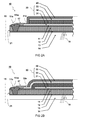
- FIGs 2A and 2B show schematic cross-section views of embodiments of a barrier foil 10 with integrated electrical circuit 17a,17b electrically connected to an electrical device stack 30 disposed on top of the foil 10.
- an electrode layer 31,33 of the device structure 30 is electrically connected to the sealing material 17m.
- FIG 2A illustrates how a bottom electrode 31 of the device stack 30 is connected by a shunt 47 to the sealing material 17m.
- FIG 2B illustrates how a top electrode 33 of the device stack 30 is connected by a shunt 47 to the sealing material 17m.
- a part 31e,33e of the respective electrode layer 31,33 extends from underneath a sealing layer 40 applied on top of the device structure 30 wherein the extended part of the electrode layer is electrically connected to the sealing material 17m. While the present embodiments show the device stack connected by a separate shunt material, alternatively, or in addition, the layer 31 or 33 can be directly in contact with the sealing material 17m.
- the device stack 30 comprises an electro-optical layer 32 between the electrode layers 31 and 33.
- the electro-optical layer 32 may e.g. comprise a light emitting layer or a light absorbing layer.
- the device stack 30 may form part of an OLED or OPV device.
- the barrier foil formed by the layers 11,12,13 may prevent external moisture and/or oxygen 19 from reaching the device stack, at least from the bottom.
- the sealing material 17m may prevent the external moisture and/or oxygen 19 from penetrating the organic layer 12 from a side 21 of the foil. At the same time the sealing material 17m may form part of the electrical circuit of the device stack 30.
- the present disclosure provides a barrier foil 10.
- the barrier foil comprises a layered structure comprising an organic layer 12 sandwiched between barrier layers 11, 13.
- the barrier foil 10 comprises a sealed groove 17 alongside a perimeter of the barrier foil 10.
- the sealed groove 17 is formed by an elongated groove 16 extending partially through the barrier foil segment 10 from a face 10a of the barrier foil 10, partly or all the way through at least the organic layer 12.
- the elongated groove 16 filled with a sealing material 17m.
- the sealed groove 17 and the barrier layers 11, 13 are arranged for enclosing organic material 12m in at least part of the organic layer 12 and adapted for preventing, in use, external moisture and/or oxygen 19 from reaching the organic material 12m.
- the sealing material 17m comprises an electrically conductive material forming an electrical circuit.
- the barrier foil is part of OLED or OPV device stack.
- the device stack may further comprise one or more electro-optical layers 31,32,33 disposed on a face of the barrier foil 10.
- the barrier foil 10 is configured to seal the electro-optical layers at least from one side for preventing external moisture and/or oxygen 19 from reaching the electro-optical device structure 30.
- the sealing material 17m forms an electrical circuit, e.g. busbar, that is electrically connected to the electro-optical device structure 30.
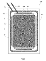
- FIG 3 shows a schematic top view of a foil segment 10 with electrical connections 57a,57b applied to the circuit.
- the sealed groove 17a extends along a perimeter 15.
- a device stack 30 is disposed on the foil inside the perimeter of the foil.
- a first electrode 31 of the device stack 30 is electrically connected to a first sealed groove 17a in the barrier foil.
- a second electrode 32 of the device stack 30 is electrically connected to a second sealed groove 17b in the barrier foil. Either one or both of the electrical connections may be facilitated by a shunt 31a,31b.
- one or more sealed grooves 17a,17b are electrically connected to an external power source or power drain, e.g.
- electrodes 57a and 57b e.g. to power the device 30 or receive electrical energy therefrom.
- the figure shows a rectangular foil segment, this may be any other desired shape such as a square, triangle, circle, oval, star, or any custom shape.
- the sealed groove / busbar may generally follow a contour of the segment perimeter 15, e.g. being approximately parallel to the segment perimeter 15.
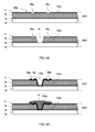
- FIG 4A shows a schematic embodiment of a method for cutting into a barrier foil.
- the method comprises (B1) providing two shallow cuts 16s in the barrier foil 10 from one face 10a of the barrier foil 10 into at least a top barrier layer 11.
- the method further comprises (B2) cutting in between the shallow cuts 16s forming the elongated groove 16 at least partially through the organic layer 12 of the barrier foil 10.
- the elongated groove 16 is cut deeper into the barrier foil than the shallow cuts 16s.
- FIG 4B shows a schematic embodiment for filling cuts in the barrier foil.
- the method comprises (C1) depositing a wetting material 17w at least into the elongated groove 16 before depositing the sealing material 17m, for improving bonding of the sealing material 17m in the groove 16 by means of the wetting material 17w.
- the method comprises (C2) depositing the sealing material 17m to cover both the shallow cuts 16s and the elongated groove 16. It is noted that the depositing of the wetting layer 17 (step C1) may also be omitted when covering the grooves 16s and 16 with sealing material 17m.
- FIG 5 shows a system 100 for providing an electrical circuit on a barrier foil 10.
- the system comprises a foil providing means 50, 60, a groove forming means 52, a groove sealing means 53, and a controller 70.
- the controller 70 is arranged (i.e. programmed and connected) for controlling the foil providing means 50, 60 for providing the continuous barrier foil 10.
- the continuous barrier foil 10 comprises a continuous layered structure comprising an organic layer 12 sandwiched between barrier layers 11 and 13.
- the controller 70 is further arranged for controlling the groove forming means 52 for partially cutting through the continuous barrier foil 10 forming an elongated groove 16 into the continuous barrier foil 10.
- the elongated groove 16 thus cut extends alongside a predefined segment perimeter 15 on the continuous barrier foil 10.
- the elongated groove 16 extends from one face of the continuous barrier foil 10 all the way through at least one of the barrier layers (11) and the organic layer 12.
- the controller in combination with the groove forming means are thus arranged to cut at least through the barrier layer 11 and the organic layer 12.
- the controller may e.g. comprise a memory with instructions for determining an absolute or relative position of the predefined segment perimeter 15 and/or the elongated groove 16.
- the instructions may also comprise a duration and/or cutting power applied by the groove forming means 52 on the layered structure to cut at least through the barrier layer 11 and the organic layer 12
- the controller 70 is further arranged for controlling the groove sealing means 53 for depositing a sealing material into the elongated groove 16 thus forming a sealed groove 17 alongside the segment perimeter 15.
- the sealed groove 17 and the barrier layers 11, 13 are arranged for enclosing organic material 12m in at least part of the organic layer 12 and adapted for preventing, in use, external moisture and/or oxygen from reaching the organic material 12m when the barrier foil segment 20 is cut from the continuous barrier foil 10 along the pre-defined segment perimeter 15 through the continuous barrier foil 10.
- the groove sealing means 53 comprises a supply with an electrically conductive material as the sealing material 17m for forming the electrical circuit by means of the deposited sealing material 17m.
- the system further comprises a foil cutting means 54.
- the controller 70 is further arranged for controlling the groove forming means 52 to form the elongated groove 16 extending alongside a predefined segment perimeter 15 on the barrier foil 10, the elongated groove 16 extending from one face 10a of the barrier foil 10 all the way through at least the said organic layer 12
- the controller 70 is further arranged for controlling the foil cutting means 54 for cutting through the barrier foil 10 along the segment perimeter 15.
- the sealed groove 17 formed parallel to the predefined segment perimeter 15 and adapted for preventing, in use, external moisture and/or oxygen 19 from reaching the organic material 12m when the barrier foil segment 20 is cut along the pre-defined segment perimeter 15 through the barrier foil 10.
- the foil 10 may also be kept intact e.g. for further processing or storing the divided continuous foil back on a roll.
- system further comprises a shunt deposition means 57.
- controller 70 is further arranged for controlling the shunt deposition means 57 for depositing an electrically conducting shunt 47 on top of the foil 10 wherein the shunt 47 is electrically connected to the sealing material 17m.
- the system 100 further comprises layer deposition means 51, arranged for providing one or more layers onto a foil substrate 14.
- the controller 70 is arranged for controlling the layer deposition means 51 for depositing a continuous layered structure on the foil substrate 14.
- the continuous layered structure comprises an organic layer 12 sandwiched between barrier layers 11,13 forming the continuous barrier foil 10.
- the layer deposition means 51 comprises a barrier layer deposition means and an organic layer deposition means.
- the barrier layer deposition means comprises a barrier material supply that is, in use, filled with a barrier material to be deposited on the substrate 14 to form the barrier layers 11 and/or 13.
- the organic layer deposition means comprises an organic material supply that is, in use, filled with organic material to be deposited on the substrate 14 to form the organic layer 12.
- the foil providing means comprises a foil supply 50 on a roll and a foil transport system 60, wherein the foil transport system 60 carries the foil along the said sequence of foil treatments, wherein the sequence comprises a groove forming means arranged to form a groove in the barrier foil after a outer top barrier layer 11 is deposited on the organic layer 12 by a barrier layer deposition means.
- the foil substrate 14 is supplied from a foil supply roll 50 and transported by a foil conveyor system 60, e.g. an endless conveyor belt moving the foil in direction 61. Also other known means for transporting a foil may be used, e.g. rollers.
- the layers deposited onto the substrate 14 may form the continuous barrier foil 10.
- the substrate 14 may be part of the continuous barrier foil 10 or may be removed after layer deposition.
- the continuous barrier foil 10 may also be directly provided, e.g. from a supply roll comprising the continuous barrier foil 10.
- the continuous barrier foil 10 may e.g. be manufactured in a preceding R2R process.
- the continuous barrier foil 10 may also be provided as a sheet.
- a continuous barrier foil sheet may be divided into barrier foil segments by the system and process described herein.
- a foil segment 20 can be divided and cut from a continuous barrier foil sheet 10.
- a foil providing means may thus include any and all means for providing a foil.
- the system 100 further comprises an enclosure 56.
- the continuous barrier foil is processed inside the enclosure.
- An environmental control system 55 may be used to provide a low-humidity and/or low oxygen environment inside the enclosure 56.
- the continuous barrier foil 10 While the continuous barrier foil 10 is cut it may be kept from external moisture and/or oxygen 19 by environmental control system 55 and/or the enclosure 56. For example, dry nitrogen may be flushed through the enclosure for providing an environment with low humidity and low oxygen. Alternatively or in addition, the enclosure may be kept at low pressure, e.g. vacuum.
- the partially cutting B the continuous barrier foil 10 may thus be preceded by bringing the foil into an environment having low moisture and/or low oxygen adapted to prevent deterioration of the organic material 12m when exposed to said environment.
- the foil is further processed in processing system 101.
- Further processing may include additional layer deposition.
- Further processing may take place on cut foil segments or on a non-cut foil.
- An advantage of cutting the foil segments may be to more easily handle them, e.g. when gluing separate foil segments. Keeping the divided foil segments together in a continuous foil facilitates further R2R processing.
- an OLED layer is deposited onto the divided barrier foil segments 20.
- the OLED layer may comprise additional layers such as, but not limited to light emitting layers, cathode and anode layers, and/or charge injection layers.
- the OLED layer may be covered by a second barrier foil layer.
- the second barrier foil layer may be deposited onto the OLED layer or glued to the OLED layer.
- the barrier foil segments may enclose the OLED layer.
- the barrier foil segments may be fused together or sealed in another way at the edges. In this way the OLED layer may be protected from moisture and/or oxygen.
- the continuous barrier foil comprises an OLED layer as one of its organic layers. The OLED layer is thus sealed by sealing the continuous barrier foil.
- While example systems were shown for providing a foil, digging grooves in a foil, sealing the grooves, depositing further layers, and/or cutting a foil, also alternative systems and means may be used for achieving similar results. Whereas in the discussion, reference is made to a foil, the same methods and systems may be applicable to other structures, e.g. rigid substrates and layers. Optical components such as lasers, mirrors, lenses, etc may be combined or split up into one or more alternative optical components having similar effect. Similarly electrical components such as controllers and processors may be split into separate and/or dedicated components or be comprised in integrated circuitry.
- the present disclosure may also find application in sealing other types of layered structures.
Landscapes
- Chemical & Material Sciences (AREA)
- Inorganic Chemistry (AREA)
- Physics & Mathematics (AREA)
- Optics & Photonics (AREA)
- Electroluminescent Light Sources (AREA)
Priority Applications (3)
| Application Number | Priority Date | Filing Date | Title |
|---|---|---|---|
| EP14198191.0A EP3035404A1 (de) | 2014-12-16 | 2014-12-16 | Barrierenfolie mit elektrischem Stromkreis |
| PCT/NL2015/050845 WO2016099255A1 (en) | 2014-12-16 | 2015-12-04 | Barrier foil comprising an electrical circuit |
| TW104142057A TW201640710A (zh) | 2014-12-16 | 2015-12-15 | 具有電子電路的阻障箔 |
Applications Claiming Priority (1)
| Application Number | Priority Date | Filing Date | Title |
|---|---|---|---|
| EP14198191.0A EP3035404A1 (de) | 2014-12-16 | 2014-12-16 | Barrierenfolie mit elektrischem Stromkreis |
Publications (1)
| Publication Number | Publication Date |
|---|---|
| EP3035404A1 true EP3035404A1 (de) | 2016-06-22 |
Family
ID=52133882
Family Applications (1)
| Application Number | Title | Priority Date | Filing Date |
|---|---|---|---|
| EP14198191.0A Withdrawn EP3035404A1 (de) | 2014-12-16 | 2014-12-16 | Barrierenfolie mit elektrischem Stromkreis |
Country Status (3)
| Country | Link |
|---|---|
| EP (1) | EP3035404A1 (de) |
| TW (1) | TW201640710A (de) |
| WO (1) | WO2016099255A1 (de) |
Cited By (5)
| Publication number | Priority date | Publication date | Assignee | Title |
|---|---|---|---|---|
| CN109065552A (zh) * | 2018-08-03 | 2018-12-21 | 武汉华星光电半导体显示技术有限公司 | Oled显示装置 |
| CN109671864A (zh) * | 2018-12-20 | 2019-04-23 | 武汉华星光电技术有限公司 | Oled显示面板 |
| CN110556407A (zh) * | 2019-08-30 | 2019-12-10 | 武汉天马微电子有限公司 | 一种显示面板及显示装置 |
| DE102020130230A1 (de) | 2020-11-16 | 2022-05-19 | Lightpat Gmbh | Anordnung umfassend organische Leuchtdioden auf einem flexiblen Substrat |
| DE102020008109A1 (de) | 2020-11-16 | 2022-05-19 | Lightpat Gmbh | Anordnung umfassend organische Leuchtdioden auf einem flexiblen Substrat |
Families Citing this family (3)
| Publication number | Priority date | Publication date | Assignee | Title |
|---|---|---|---|---|
| CN109065644A (zh) * | 2018-08-15 | 2018-12-21 | 汉能新材料科技有限公司 | 一种太阳能电池 |
| CN109873022B (zh) | 2019-03-21 | 2021-01-22 | 京东方科技集团股份有限公司 | 一种背板、显示装置以及背板的制备方法 |
| CN113192983B (zh) * | 2021-04-19 | 2022-12-06 | 武汉华星光电半导体显示技术有限公司 | 显示面板及其制备方法 |
Citations (3)
| Publication number | Priority date | Publication date | Assignee | Title |
|---|---|---|---|---|
| EP2151876A1 (de) * | 2008-08-05 | 2010-02-10 | Nederlandse Organisatie voor toegepast- natuurwetenschappelijk onderzoek TNO | Elektrische Transportkomponente, Herstellungsverfahren dafür sowie elektro-optische Vorrichtung und opto-elektrische Vorrichtung |
| WO2014011044A1 (en) | 2012-07-12 | 2014-01-16 | Nederlandse Organisatie Voor Toegepast-Natuurwetenschappelijk Onderzoek Tno | Method and system for dividing a barrier foil |
| US20140206177A1 (en) * | 2013-01-23 | 2014-07-24 | Disco Corporation | Wafer processing method |
-
2014
- 2014-12-16 EP EP14198191.0A patent/EP3035404A1/de not_active Withdrawn
-
2015
- 2015-12-04 WO PCT/NL2015/050845 patent/WO2016099255A1/en not_active Ceased
- 2015-12-15 TW TW104142057A patent/TW201640710A/zh unknown
Patent Citations (3)
| Publication number | Priority date | Publication date | Assignee | Title |
|---|---|---|---|---|
| EP2151876A1 (de) * | 2008-08-05 | 2010-02-10 | Nederlandse Organisatie voor toegepast- natuurwetenschappelijk onderzoek TNO | Elektrische Transportkomponente, Herstellungsverfahren dafür sowie elektro-optische Vorrichtung und opto-elektrische Vorrichtung |
| WO2014011044A1 (en) | 2012-07-12 | 2014-01-16 | Nederlandse Organisatie Voor Toegepast-Natuurwetenschappelijk Onderzoek Tno | Method and system for dividing a barrier foil |
| US20140206177A1 (en) * | 2013-01-23 | 2014-07-24 | Disco Corporation | Wafer processing method |
Cited By (8)
| Publication number | Priority date | Publication date | Assignee | Title |
|---|---|---|---|---|
| CN109065552A (zh) * | 2018-08-03 | 2018-12-21 | 武汉华星光电半导体显示技术有限公司 | Oled显示装置 |
| WO2020024347A1 (zh) * | 2018-08-03 | 2020-02-06 | 武汉华星光电半导体显示技术有限公司 | Oled显示装置 |
| CN109671864A (zh) * | 2018-12-20 | 2019-04-23 | 武汉华星光电技术有限公司 | Oled显示面板 |
| CN109671864B (zh) * | 2018-12-20 | 2020-06-30 | 武汉华星光电技术有限公司 | Oled显示面板 |
| CN110556407A (zh) * | 2019-08-30 | 2019-12-10 | 武汉天马微电子有限公司 | 一种显示面板及显示装置 |
| DE102020130230A1 (de) | 2020-11-16 | 2022-05-19 | Lightpat Gmbh | Anordnung umfassend organische Leuchtdioden auf einem flexiblen Substrat |
| DE102020008109A1 (de) | 2020-11-16 | 2022-05-19 | Lightpat Gmbh | Anordnung umfassend organische Leuchtdioden auf einem flexiblen Substrat |
| WO2022101241A2 (de) | 2020-11-16 | 2022-05-19 | Lightpat Gmbh | Anordnung umfassend organische leuchtdioden auf einem flexiblen substrat |
Also Published As
| Publication number | Publication date |
|---|---|
| WO2016099255A1 (en) | 2016-06-23 |
| TW201640710A (zh) | 2016-11-16 |
Similar Documents
| Publication | Publication Date | Title |
|---|---|---|
| WO2016099255A1 (en) | Barrier foil comprising an electrical circuit | |
| EP2873104B1 (de) | Verfahren und system zur aufteilung einer grenzfolie | |
| RU2697573C2 (ru) | Способ изготовления устройства тонкопленочных солнечных элементов и такое устройство тонкопленочных солнечных элементов | |
| JP5834009B2 (ja) | モノリシック並列相互接続構造 | |
| KR101896139B1 (ko) | 광전자 디바이스 패키지, 어레이 및 제조 방법 | |
| TWI433339B (zh) | 薄膜太陽能電池模組之製造方法及薄膜太陽能電池模組 | |
| TWI433340B (zh) | 半導體元件以及增加半導體元件有效運作面積的方法 | |
| CN102598268A (zh) | 薄层太阳能电池的串接方法 | |
| CN103843149B (zh) | 包括有涂覆步骤的制造结构的方法和对应的结构及装置 | |
| TW201242042A (en) | Process for forming flexible substrates having patterned contact areas | |
| US20150108433A1 (en) | Organic light-emitting diode display and manufacturing method thereof | |
| US11581502B2 (en) | Method of making a current collecting grid for solar cells | |
| EP2510563A2 (de) | Elektrooptische vorrichtung, elektrode dafür sowie verfahren und vorrichtung zur herstellung einer elektrode und der elektrooptischen vorrichtung damit | |
| US20150367616A1 (en) | Pressure-transferred components | |
| CN102456769B (zh) | 半导体元件以及增加半导体元件有效运作面积的方法 | |
| US12290879B2 (en) | Method for creating shunt free translucent flexible thin-film photovoltaic module | |
| US10651430B2 (en) | Organic electronic element manufacturing method and organic electronic element | |
| US20170012239A1 (en) | Light emitting apparatus | |
| EP3358914A1 (de) | Verfahren zur herstellung eines organischen elements | |
| CN111095593A (zh) | 用于无掩模oled沉积和制造的方法 | |
| CN121358006A (zh) | 一种单玻光伏组件的制备方法及光伏组件 | |
| JP2013258176A (ja) | 光電変換装置の製造方法 | |
| GB2533127A (en) | A flexible thin film electronic device |
Legal Events
| Date | Code | Title | Description |
|---|---|---|---|
| PUAI | Public reference made under article 153(3) epc to a published international application that has entered the european phase |
Free format text: ORIGINAL CODE: 0009012 |
|
| AK | Designated contracting states |
Kind code of ref document: A1 Designated state(s): AL AT BE BG CH CY CZ DE DK EE ES FI FR GB GR HR HU IE IS IT LI LT LU LV MC MK MT NL NO PL PT RO RS SE SI SK SM TR |
|
| AX | Request for extension of the european patent |
Extension state: BA ME |
|
| STAA | Information on the status of an ep patent application or granted ep patent |
Free format text: STATUS: THE APPLICATION IS DEEMED TO BE WITHDRAWN |
|
| 18D | Application deemed to be withdrawn |
Effective date: 20161223 |