EP3035510A2 - Verfahren und vorrichtung zur modulierung eines fünfstufigen umrichters und fotovoltaiksystem - Google Patents
Verfahren und vorrichtung zur modulierung eines fünfstufigen umrichters und fotovoltaiksystem Download PDFInfo
- Publication number
- EP3035510A2 EP3035510A2 EP15193963.4A EP15193963A EP3035510A2 EP 3035510 A2 EP3035510 A2 EP 3035510A2 EP 15193963 A EP15193963 A EP 15193963A EP 3035510 A2 EP3035510 A2 EP 3035510A2
- Authority
- EP
- European Patent Office
- Prior art keywords
- switching device
- switched
- v1neg
- v1pos
- dthrs
- Prior art date
- Legal status (The legal status is an assumption and is not a legal conclusion. Google has not performed a legal analysis and makes no representation as to the accuracy of the status listed.)
- Ceased
Links
Images


Classifications
-
- H—ELECTRICITY
- H02—GENERATION; CONVERSION OR DISTRIBUTION OF ELECTRIC POWER
- H02M—APPARATUS FOR CONVERSION BETWEEN AC AND AC, BETWEEN AC AND DC, OR BETWEEN DC AND DC, AND FOR USE WITH MAINS OR SIMILAR POWER SUPPLY SYSTEMS; CONVERSION OF DC OR AC INPUT POWER INTO SURGE OUTPUT POWER; CONTROL OR REGULATION THEREOF
- H02M7/00—Conversion of AC power input into DC power output; Conversion of DC power input into AC power output
- H02M7/42—Conversion of DC power input into AC power output without possibility of reversal
- H02M7/44—Conversion of DC power input into AC power output without possibility of reversal by static converters
- H02M7/48—Conversion of DC power input into AC power output without possibility of reversal by static converters using discharge tubes with control electrode or semiconductor devices with control electrode
- H02M7/483—Converters with outputs that each can have more than two voltages levels
- H02M7/487—Neutral point clamped inverters
-
- H—ELECTRICITY
- H02—GENERATION; CONVERSION OR DISTRIBUTION OF ELECTRIC POWER
- H02M—APPARATUS FOR CONVERSION BETWEEN AC AND AC, BETWEEN AC AND DC, OR BETWEEN DC AND DC, AND FOR USE WITH MAINS OR SIMILAR POWER SUPPLY SYSTEMS; CONVERSION OF DC OR AC INPUT POWER INTO SURGE OUTPUT POWER; CONTROL OR REGULATION THEREOF
- H02M7/00—Conversion of AC power input into DC power output; Conversion of DC power input into AC power output
- H02M7/42—Conversion of DC power input into AC power output without possibility of reversal
- H02M7/44—Conversion of DC power input into AC power output without possibility of reversal by static converters
- H02M7/48—Conversion of DC power input into AC power output without possibility of reversal by static converters using discharge tubes with control electrode or semiconductor devices with control electrode
- H02M7/483—Converters with outputs that each can have more than two voltages levels
-
- H—ELECTRICITY
- H02—GENERATION; CONVERSION OR DISTRIBUTION OF ELECTRIC POWER
- H02M—APPARATUS FOR CONVERSION BETWEEN AC AND AC, BETWEEN AC AND DC, OR BETWEEN DC AND DC, AND FOR USE WITH MAINS OR SIMILAR POWER SUPPLY SYSTEMS; CONVERSION OF DC OR AC INPUT POWER INTO SURGE OUTPUT POWER; CONTROL OR REGULATION THEREOF
- H02M7/00—Conversion of AC power input into DC power output; Conversion of DC power input into AC power output
- H02M7/42—Conversion of DC power input into AC power output without possibility of reversal
- H02M7/44—Conversion of DC power input into AC power output without possibility of reversal by static converters
- H02M7/48—Conversion of DC power input into AC power output without possibility of reversal by static converters using discharge tubes with control electrode or semiconductor devices with control electrode
- H02M7/53—Conversion of DC power input into AC power output without possibility of reversal by static converters using discharge tubes with control electrode or semiconductor devices with control electrode using devices of a triode or transistor type requiring continuous application of a control signal
- H02M7/537—Conversion of DC power input into AC power output without possibility of reversal by static converters using discharge tubes with control electrode or semiconductor devices with control electrode using devices of a triode or transistor type requiring continuous application of a control signal using semiconductor devices only, e.g. single switched pulse inverters
- H02M7/539—Conversion of DC power input into AC power output without possibility of reversal by static converters using discharge tubes with control electrode or semiconductor devices with control electrode using devices of a triode or transistor type requiring continuous application of a control signal using semiconductor devices only, e.g. single switched pulse inverters with automatic control of output wave form or frequency
- H02M7/5395—Conversion of DC power input into AC power output without possibility of reversal by static converters using discharge tubes with control electrode or semiconductor devices with control electrode using devices of a triode or transistor type requiring continuous application of a control signal using semiconductor devices only, e.g. single switched pulse inverters with automatic control of output wave form or frequency by pulse-width modulation
-
- H—ELECTRICITY
- H02—GENERATION; CONVERSION OR DISTRIBUTION OF ELECTRIC POWER
- H02S—GENERATION OF ELECTRIC POWER BY CONVERSION OF INFRARED RADIATION, VISIBLE LIGHT OR ULTRAVIOLET LIGHT, e.g. USING PHOTOVOLTAIC [PV] MODULES
- H02S40/00—Components or accessories in combination with PV modules, not provided for in groups H02S10/00 - H02S30/00
-
- H—ELECTRICITY
- H02—GENERATION; CONVERSION OR DISTRIBUTION OF ELECTRIC POWER
- H02M—APPARATUS FOR CONVERSION BETWEEN AC AND AC, BETWEEN AC AND DC, OR BETWEEN DC AND DC, AND FOR USE WITH MAINS OR SIMILAR POWER SUPPLY SYSTEMS; CONVERSION OF DC OR AC INPUT POWER INTO SURGE OUTPUT POWER; CONTROL OR REGULATION THEREOF
- H02M1/00—Details of apparatus for conversion
- H02M1/0095—Hybrid converter topologies, e.g. NPC mixed with flying capacitor, thyristor converter mixed with MMC or charge pump mixed with buck
-
- H—ELECTRICITY
- H02—GENERATION; CONVERSION OR DISTRIBUTION OF ELECTRIC POWER
- H02M—APPARATUS FOR CONVERSION BETWEEN AC AND AC, BETWEEN AC AND DC, OR BETWEEN DC AND DC, AND FOR USE WITH MAINS OR SIMILAR POWER SUPPLY SYSTEMS; CONVERSION OF DC OR AC INPUT POWER INTO SURGE OUTPUT POWER; CONTROL OR REGULATION THEREOF
- H02M1/00—Details of apparatus for conversion
- H02M1/12—Arrangements for reducing harmonics from AC input or output
-
- H—ELECTRICITY
- H02—GENERATION; CONVERSION OR DISTRIBUTION OF ELECTRIC POWER
- H02M—APPARATUS FOR CONVERSION BETWEEN AC AND AC, BETWEEN AC AND DC, OR BETWEEN DC AND DC, AND FOR USE WITH MAINS OR SIMILAR POWER SUPPLY SYSTEMS; CONVERSION OF DC OR AC INPUT POWER INTO SURGE OUTPUT POWER; CONTROL OR REGULATION THEREOF
- H02M3/00—Conversion of DC power input into DC power output
-
- Y—GENERAL TAGGING OF NEW TECHNOLOGICAL DEVELOPMENTS; GENERAL TAGGING OF CROSS-SECTIONAL TECHNOLOGIES SPANNING OVER SEVERAL SECTIONS OF THE IPC; TECHNICAL SUBJECTS COVERED BY FORMER USPC CROSS-REFERENCE ART COLLECTIONS [XRACs] AND DIGESTS
- Y02—TECHNOLOGIES OR APPLICATIONS FOR MITIGATION OR ADAPTATION AGAINST CLIMATE CHANGE
- Y02E—REDUCTION OF GREENHOUSE GAS [GHG] EMISSIONS, RELATED TO ENERGY GENERATION, TRANSMISSION OR DISTRIBUTION
- Y02E10/00—Energy generation through renewable energy sources
- Y02E10/50—Photovoltaic [PV] energy
- Y02E10/56—Power conversion systems, e.g. maximum power point trackers
Definitions
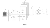
- the present disclosure relates to the technical field of photovoltaic power generation, and in particular to a method for modulating a five-level inverter, a device for modulating a five-level inverter, and a photovoltaic system.
- a direct current side of a five-level inverter 10 is connected to a photovoltaic array 20 and configured to receive a PV input voltage at the direct current side.
- the PV input voltage is applied across a positive electrode of a capacitor C1 and a negative electrode of a capacitor C2, voltages of C1 and C2 relative to a middle point of DC-bus are V1Pos and V1Neg respectively.
- the PV input voltage is step up by two Boost circuits at the front of the five-level inverter 10, then is applied across a positive electrode of a bus capacitor C3 and a negative electrode of a bus capacitor C4, and voltages of C3 and C4 relative to the middle point of the DC-bus are V2Pos and V2Neg respectively.
- An output voltage from the grid side of the five-level inverter 10 is filtered by a filter 30, step up by a transformer 40 and then transmitted to a power grid.
- the five-level inverter 10 alternately outputs levels +V1Pos, -V1Neg, +V2Pos, -V2Neg and a zero level corresponding to the middle point of the DC-bus.
- the modulation may include four modulation sections:
- a corresponding duty ratio command value Dcmd meets 1-Vx/V1Pos ⁇ Dcmd ⁇ 1; in a case that Vcmd is greater than 0 and approaches V1Pos from a value less than V1Pos, Dcmd is close to 1, thereby resulting in many narrow pulses; and in a case that Vx/V1Pos is less than the duty ratio Dthrs corresponding to the sum of narrow pulse time and dead-band time, in order to ensure that switching devices operate safely, these narrow pulses need to be deleted and Dcmd is clamped to 1.
- Vcmd is greater than 0 and approaches +V1Pos from a value greater than +V1Pos
- Vcmd is less than 0 and approaches -V1Neg from a value greater than -V1Neg
- Vcmd is less than 0 and approaches -V1Neg from a value less than -V1Neg
- Vcmd approaches 0 there are also many narrow pulses to be deleted.
- deleting of narrow pulses results in distortion of the phase bridge output voltage.
- a method for modulating a five-level inverter, a device for modulating a five-level inverter, and a photovoltaic system are provided according to the present disclosure, to reduce the number of narrow pulses generated during modulating of the five-level inverter, thereby reducing the impact on the distortion of the phase bridge output voltage of the five-level inverter due to deleting of the narrow pulses, and the safety operation of the switching devices is guaranteed at the same time.
- a method for modulating a five-level inverter which includes:
- Vthrs1 Dthrs*(V2Pos-V1Pos)
- Vthrs2 Dthrs*V1Pos
- Vthrs3 Dthrs*V1Neg
- Vthrs4 Dthrs*(V2Neg-V1Neg).
- a method for modulating a five-level inverter which includes:
- Vthrs1 Dthrs*(V2Pos-V1Pos)
- Vthrs2 Dthrs*V1Pos
- Vthrs3 Dthrs*V1Neg
- Vthrs4 Dthrs*(V2Neg-V1Neg)
- Vthrs5 Dthrs*V1Pos
- Vthrs6 Dthrs*V1Neg.
- a device for modulating a five-level inverter which includes:
- Vthrs1 Dthrs*(V2Pos-V1Pos)
- Vthrs2 Dthrs*V1Pos
- Vthrs3 Dthrs*V1Neg
- Vthrs4 Dthrs*(V2Neg-V1Neg).
- a device for modulating a five-level inverter which includes:
- Vthrs1 Dthrs*(V2Pos-V1Pos)
- Vthrs2 Dthrs*V1Pos
- Vthrs3 Dthrs*V1Neg
- Vthrs4 Dthrs*(V2Neg-V1Neg)
- Vthrs5 Dthrs*V1Pos
- Vthrs6 Dthrs*V1Neg.
- a photovoltaic system which includes a photovoltaic array, two Boost circuits, a five-level inverter, a filter and a transformer, where a direct current side of the five-level inverter is connected to the photovoltaic array, and the grid side of the five-level inverter is connected to the power grid via the filter and the transformer; and the photovoltaic system further includes a controller connected to the five-level inverter, and the controller is configured to: acquire a voltage command value Vcmd of the phase bridge of the five-level inverter; control a first switching device and a fourth switching device to be switched on alternately in a case that Vcmd ⁇ V1Pos+Vthrs1; control the first switching device and a third switching device to be switched on alternately in a case that V1Pos-Vthrs2 ⁇ Vcmd ⁇ V1Pos+Vthrs1; control the fourth switching device and the third switching device to be switched on alternately in a case that 0 ⁇
- a photovoltaic system which includes a photovoltaic array, two Boost circuits, a five-level inverter, a filter and a transformer, where a direct current side of the five-level inverter is connected to the photovoltaic array via the two Boost circuits, and a grid side of the five-level inverter is connected to a power grid via the filter and the transformer; and the photovoltaic system further includes a controller connected to the five-level inverter, and the controller is configured to: acquire a voltage command value Vcmd of a phase bridge of the five-level inverter; control a first switching device and a fourth switching device to be switched on alternately in a case that Vcmd ⁇ V1Pos+Vthrs1; control the first switching device and a third switching device to be switched on alternately in a case that V1Pos-Vthrs2 ⁇ Vcmd ⁇ V1Pos+Vthrs1; control the fourth switching device and the third switching device to be switched on on
- the output voltage level of the five-level inverter is switched cross levels according to the present disclosure rather than between adjacent levels, such that the duty ratio is far away from 0 or 1 rather than approaching 0 or 1, thereby preventing generating narrow pulses in a case that Vcmd approaches +V1Pos or -V1Neg.
- the narrow pulses are generated in a case that Vcmd approaches +V1Pos, -V1Neg or 0; and according to the present disclosure, the number of the narrow pulses generated during modulating of the five-level inverter is reduced significantly, thereby reducing the impact on the distortion of the phase bridge output voltage of the five-level inverter due to deleting of the narrow pulses, and the safety operation of the switching devices is guaranteed at the same time.
- a method for modulating a five-level inverter is disclosed, to reduce the number of narrow pulses generated during modulating of the five-level inverter, thereby reducing the impact on the distortion of the phase bridge output voltage of the five-level inverter due to deleting of the narrow pulses, and the safety operation of the switching devices is guaranteed at the same time.
- a five-level inverter 10 alternately outputs five voltage levels +1, -1, +2, -2 and 0 in different combinations of switching states of switching devices, and values of the five voltage levels are +V1Pos, -V1Neg, +V2Pos, -V2Neg and 0 respectively.
- S2Pos indicates a first switching device, the level +2 is outputted when the first switching device is switched on;
- S2Neg indicates a second switching device, the level -2 is outputted when the second switching device is switched on;
- SO indicates a third switching device, the level 0 is outputted when the third switching device is switched on;
- S1Pos indicates a fourth switching device, the level +1 is outputted when the fourth switching device is switched on;
- S1Neg indicates a fifth switching device, the level -1 is outputted when the fifth switching device is switched on.
- Dthrs indicates a duty ratio corresponding to the sum of narrow pulse time and dead-band time of the five-level inverter 10, which is a known constant.
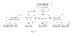
- the method for modulating a five-level inverter may include step S201 to step S212 hereinafter.
- step S201 a voltage command value Vcmd of a phase bridge of the five-level inverter is acquired.
- step 202 it is determined whether Vcmd ⁇ 0 is met; and if Vcmd ⁇ 0 is met, the method proceeds to step S203; otherwise, the method proceeds to step S205.
- step S203 it is determined whether Vcmd ⁇ V1Pos+Vthrs1 is met; and if Vcmd ⁇ V1Pos+Vthrs1 is met, the method proceeds to step S207; otherwise, the method proceeds to step S204, where Vthrs1 ⁇ Dthrs*(V2Pos-V1Pos).
- step S204 it is determined whether V1Pos-Vthrs2 ⁇ Vcmd ⁇ V1Pos+Vthrs1 is met; if V1Pos-Vthrs2 ⁇ Vcmd ⁇ V1Pos+Vthrs1 is met, the method proceeds to step 208; otherwise the method proceeds to step 209, where Vthrs2 ⁇ Dthrs*V1Pos.
- step S205 it is determined whether -V1Neg+Vthrs3 ⁇ Vcmd ⁇ 0 is met; and if -V1Neg+Vthrs3 ⁇ Vcmd ⁇ 0 is met, the method proceeds to step 210; otherwise, the method proceeds to step 206, where Vthrs3 ⁇ Dthrs*V1Neg.
- step 206 it is determined whether -V1Neg-Vthrs4 ⁇ Vcmd ⁇ -V1Neg+Vthrs3 is met; and if -V1Neg-Vthrs4 ⁇ Vcmd ⁇ -V1Neg+Vthrs3 is met, the method proceeds to step 211; otherwise, the method proceeds to step 212, where Vthrs4 ⁇ Dthrs*(V2Neg-V1Neg).
- step 207 a first modulation section is entered, in which the switching device S2Pos and the switching device S1Pos are controlled to be switched on alternately, and an output voltage level is switched between +V2Pos and +V1Pos.
- step 208 a second modulation section is entered, in which the switching device S2Pos and the switching device SO are controlled to be switched on alternately, and the output voltage level is switched between +V2Pos and 0.
- step 209 a third modulation section is entered, in which the switching device S1Pos and the switching device SO are controlled to be switched on alternately, and the output voltage level is switched between +V1Pos and 0.
- step 210 a fourth modulation section is entered, in which the switching device SO and the switching device S1Neg are controlled to be switched on alternately, and the output voltage level is switched between 0 and -V1Neg.
- step 211 a fifth modulation section is entered, in which the switching device SO and the switching device S2Neg are controlled to be switched on alternately, and the output voltage level is switched between 0 and -V2Neg.
- step 212 a sixth modulation section is entered, in which the switching device S1Neg and the switching device S2Neg are controlled to be switched on alternately, and the output voltage level is switched between -V1Neg and -V2Neg.
- duty ratio command values Dcmd for different modulation sections may be calculated based on the voltage command value Vcmd of each phase bridge (Vthrs1, Vthrs2, Vthrs3 and Vthrs4 are voltage thresholds for adjusting the modulation sections).
- Vcmd approaches -V1Neg
- the output voltage level of the five-level inverter is switched cross levels rather than between adjacent levels, such that the duty ratio is far way from 0 or 1 rather than approaching 0 or 1, thereby preventing generating narrow pulses in a case that Vcmd approaches +V1Pos or -V1Neg.
- the narrow pulses are generated only in a case that Vcmd approaches 0, the number of the narrow pulses is reduced greatly, thereby reducing the impact on the distortion of the phase bridge output voltage of the five-level inverter due to deleting of the narrow pulses, and the safety operation of the switching devices is guaranteed at the same time.
- FIG. 3 another method for modulating a five-level inverter is disclosed according to an embodiment of the present disclosure.
- the method may include step 301 to step 314 hereinafter.
- step 301 a voltage command value Vcmd of a phase bridge of the five-level inverter is acquired.
- step 302 it is determined whether Vcmd ⁇ Vthrs5 is met; and if Vcmd ⁇ Vthrs5 is met, the method proceeds to step 303; otherwise, the method proceeds to step 305.
- step 303 it is determined whether Vcmd ⁇ V1Pos+Vthrs1 is met; and if Vcmd ⁇ V1Pos+Vthrs1 is met, the method proceeds to step 308; otherwise, the method proceeds to step 304.
- step 304 it is determined whether V1Pos-Vthrs2 ⁇ Vcmd ⁇ V1Pos+Vthrs1 is met; and if V1Pos-Vthrs2 ⁇ Vcmd ⁇ V1Pos+Vthrs1 is met, the method proceeds to step 309; otherwise, the method proceeds to step 310.
- step 305 it is determined whether -Vthrs6 ⁇ Vcmd ⁇ Vthrs5 is met; and if -Vthrs6 ⁇ Vcmd ⁇ Vthrs5 is met, the method proceeds to step 311; otherwise, the method proceeds to step 306.
- step 306 it is determined whether -V1Neg+Vthrs3 ⁇ Vcmd ⁇ -Vthrs6 is met; and if -V1Neg+Vthrs3 ⁇ Vcmd ⁇ -Vthrs6 is met, the method proceeds to step 312; otherwise, the method proceeds to step 307.
- step 307 it is determined whether -V1Neg-Vthrs4 ⁇ Vcmd ⁇ -V1Neg+Vthrs3 is met; and if -V1Neg-Vthrs4 ⁇ Vcmd ⁇ -V1Neg+Vthrs3 is met, the method proceeds to step 313; otherwise, the method proceeds to step 314.
- step 308 a first modulation section is entered, in which the switching device S2Pos and the switching device S1Pos are controlled to be switched on alternately, and an output voltage level is switched between +V2Pos and +V1Pos.
- step 309 a second modulation section is entered, in which the switching device S2Pos and the switching device SO are controlled to be switched on alternately, and the output voltage level is switched between +V2Pos and 0.
- step 310 a third modulation section is entered, in which the switching device S1Pos and the switching device SO are controlled to be switched on alternately, and the output voltage level is switched between +V1Pos and 0.
- step 311 a fourth modulation section is entered, in which the switching device S1Pos and the switching device S1Neg are controlled to be switched on alternately, and the output voltage level is switched between +V1Pos and -V1Neg.
- step 312 a fifth modulation section is entered, in which the switching device SO and the switching device S1Neg are controlled to be switched on alternately, and the output voltage level is switched between 0 and -V1Neg.
- step 313 a sixth modulation section is entered, in which the switching device SO and the switching device S2Neg are controlled to be switched on alternately, and the output voltage level is switched between 0 and -V2Neg.
- step 314 a seventh modulation section is entered, in which the switching device S1Neg and the switching device S2Neg are controlled to be switched on alternately, and the output voltage level is switched between -V1Neg and -V2Neg.
- duty ratio command values Dcmd for different modulation sections may be calculated based on the voltage command value Vcmd of the phase bridge (Vthrs1, Vthrs2, Vthrs3, Vthrs4, Vthrs5 and Vthrs6 are voltage thresholds for adjusting the modulation sections).
- Vcmd approaches -V1Neg
- the output voltage level of the five-level inverter is switched cross levels rather than between adjacent levels, such that the duty ratio is far way from 0 or 1 rather than approaching 0 or 1, thereby preventing generating narrow pulses in a case that Vcmd approaches +V1Pos, -V1Neg or 0.
- the narrow pulses can be prevented from being generated both in a case that Vcmd approaches +V1Pos or -V1Neg and in a case that Vcmd approaches 0, thereby further reducing the impact on the distortion of the phase bridge output voltage of the five-level inverter due to deleting of the narrow pulses, and the safety operation of the switching devices is guaranteed at the same time.
- the modulation section to be entered is determined based on the value of Vcmd.
- the way for determining the modulation section to be entered based on Vcmd is not limited to the way disclosed above.
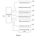
- a device for modulating a five-level inverter is further disclosed according to an embodiment of the present disclosure, to reduce the number of narrow pulses generated during modulating of the five-level inverter, thereby reducing the impact on the distortion of the phase bridge output voltage of the five-level inverter due to deleting of the narrow pulses, and the safety operation of the switching devices is guaranteed at the same time.
- the device includes an acquiring unit 401, a first processing unit 402, a second processing unit 403, a third processing unit 404, a fourth processing unit 405, a fifth processing unit 406 and a sixth processing unit 407.
- the acquiring unit 401 is configured to acquire a voltage command value Vcmd of a phase bridge of the five-level inverter.
- the first processing unit 402 is configured to control a switching device S2Pos and a switching device S1Pos to be switched on alternately in a case that Vcmd ⁇ V1Pos+Vthrs1.
- the second processing unit 403 is configured to control the switching device S2Pos and a switching device SO to be switched on alternately in a case that V1Pos-Vthrs2 ⁇ Vcmd ⁇ V1Pos+Vthrs1.
- the third processing unit 404 is configured to control the switching device S1Pos and the switching device SO to be switched on alternately in a case that 0 ⁇ Vcmd ⁇ V1Pos-Vthrs2.
- the fourth processing unit 405 is configured to control the switching device SO and a switching device S1Neg to be switched on alternately in a case that -V1Neg+Vthrs3 ⁇ Vcmd ⁇ 0.
- the fifth processing unit 406 is configured to control the switching device SO and a switching device S2Neg to be switched on alternately in a case that -V1Neg-Vthrs4 ⁇ Vcmd ⁇ -V1Neg+Vthrs3.
- the sixth processing unit 407 is configured to control the switching device S1Neg and the switching device S2Neg to be switched on alternately in a case that Vcmd ⁇ -V1Neg-Vthrs4.
- the device includes an acquiring unit 501, a first processing unit 502, a second processing unit 503, a third processing unit 504, a fourth processing unit 505, a fifth processing unit 506, a sixth processing unit 507 and a seventh processing unit 508.
- the acquiring unit 501 is configured to acquire a voltage command value Vcmd of a phase bridge of the five-level inverter.
- the first processing unit 502 is configured to control a switching device S2Pos and a switching device S1Pos to be switched on alternately in a case that Vcmd ⁇ V1Pos+Vthrs1.
- the second processing unit 503 is configured to control the switching device S2Pos and a switching device SO to be switched on alternately in a case that V1Pos-Vthrs2 ⁇ Vcmd ⁇ V1Pos+Vthrs1.
- the third processing unit 504 is configured to control the switching device S1Pos and the switching device SO to be switched on alternately in a case that Vthrs5 ⁇ Vcmd ⁇ V1Pos-Vthrs2.
- the fourth processing unit 505 is configured to control the switching device S1Pos and a switching device S1Neg to be switched on alternately in a case that -Vthrs6 ⁇ Vcmd ⁇ Vthrs5.
- the fifth processing unit 506 is configured to control the switching device SO and the switching device S1Neg to be switched on alternately in a case that -V1Neg+Vthrs3 ⁇ Vcmd ⁇ -Vthrs6.
- the sixth processing unit 507 is configured to control the switching device SO and a switching device S2Neg to be switched on alternately in a case that -V1Neg-Vthrs4 ⁇ Vcmd ⁇ -V1Neg+Vthrs3.
- the seventh processing unit 508 is configured to control the switching device S1Neg and the switching device S2Neg to be switched on alternately in a case that Vcmd ⁇ -V1Neg-Vthrs4.
- a photovoltaic system is further disclosed according to an embodiment of the present disclosure, to reduce the number of narrow pulses generated during modulating of a five-level inverter, thereby reducing the impact on the distortion of the phase bridge output voltage of the five-level inverter due to deleting of the narrow pulses, and the safety operation of the switching devices is guaranteed at the same time.
- the photovoltaic system includes a five-level inverter 10, a photovoltaic array 20, a filter 30, a transformer 40, two Boost circuits 50 and a controller 60.
- a direct current side of the five-level inverter 10 is connected to the photovoltaic array 20 via the two Boost circuits 50, and a grid side of the five-level inverter 10 is connected to a power grid via the filter 30 and the transformer 40.
- the controller 60 is connected to the five-level inverter 10 and configured to: acquire a voltage command value Vcmd of a phase bridge of the five-level inverter 10; control a switching device S2Pos and a switching device S1Pos to be switched on alternately in a case that Vcmd ⁇ V1Pos+Vthrs1; control the switching device S2Pos and a switching device SO to be switched on alternately in a case that V1Pos-Vthrs2 ⁇ Vcmd ⁇ V1Pos+Vthrs1; control the switching device S1Pos and the switching device SO to be switched on alternately in a case that 0 ⁇ Vcmd ⁇ V1Pos-Vthrs2; control the switching device SO and a switching device S1Neg to be switched on alternately in a case that -V1Neg+Vthrs3 ⁇ Vcmd ⁇ 0; control the switching device SO and a switching device S2Neg to be switched on alternately
- the photovoltaic system includes a five-level inverter, a photovoltaic array, a filter, a transformer, two Boost circuits and a controller.
- the embodiment differs from the above embodiment of the photovoltaic system in that: in the embodiment, the controller is connected to the five-level inverter and configured to: acquire a voltage command value Vcmd of a phase bridge of the five-level inverter; control a switching device S2Pos and a switching device S1Pos to be switched on alternately in a case that Vcmd ⁇ V1Pos+Vthrs1; control the switching device S2Pos and a switching device SO to be switched on alternately in a case that V1Pos-Vthrs2 ⁇ Vcmd ⁇ V1Pos+Vthrs1; control the switching device S1Pos and the switching device SO to be switched on alternately in a case that Vthrs5 ⁇ V
- the output voltage level of the five-level inverter is switched cross levels rather than between adjacent levels, such that the duty ratio is far away from 0 or 1 rather than approaching 0 or 1, thereby preventing generating narrow pulses in a case that Vcmd approaches +V1Pos or -V1Neg.
- the narrow pulses are generated in a case that Vcmd approaches +V1Pos, -V1Neg or 0; and according to the present disclosure, the number of the narrow pulses generated during modulating of the five-level inverter is reduced significantly, thereby reducing the impact on the distortion of the phase bridge output voltage of the five-level inverter due to deleting of the narrow pulses, and the safety operation of the switching devices is guaranteed at the same time.
Landscapes
- Engineering & Computer Science (AREA)
- Power Engineering (AREA)
- Inverter Devices (AREA)
Applications Claiming Priority (1)
| Application Number | Priority Date | Filing Date | Title |
|---|---|---|---|
| CN201410802612.2A CN104393778B (zh) | 2014-12-18 | 2014-12-18 | 五电平逆变器调制方法、装置以及光伏系统 |
Publications (2)
| Publication Number | Publication Date |
|---|---|
| EP3035510A2 true EP3035510A2 (de) | 2016-06-22 |
| EP3035510A3 EP3035510A3 (de) | 2016-08-03 |
Family
ID=52611628
Family Applications (1)
| Application Number | Title | Priority Date | Filing Date |
|---|---|---|---|
| EP15193963.4A Ceased EP3035510A3 (de) | 2014-12-18 | 2015-11-10 | Verfahren und vorrichtung zur modulierung eines fünfstufigen umrichters und fotovoltaiksystem |
Country Status (4)
| Country | Link |
|---|---|
| US (1) | US10044291B2 (de) |
| EP (1) | EP3035510A3 (de) |
| JP (1) | JP6197015B2 (de) |
| CN (1) | CN104393778B (de) |
Families Citing this family (6)
| Publication number | Priority date | Publication date | Assignee | Title |
|---|---|---|---|---|
| CN105207506B (zh) * | 2014-06-25 | 2017-12-29 | 华为技术有限公司 | 一种逆变器的控制方法、装置和系统 |
| CN104410307B (zh) * | 2014-12-18 | 2017-01-18 | 阳光电源股份有限公司 | 五电平逆变器的工作模式切换方法和装置 |
| WO2017138103A1 (ja) * | 2016-02-10 | 2017-08-17 | 田淵電機株式会社 | 自立運転制御装置、パワーコンディショナ及び自立運転制御方法 |
| JP6962081B2 (ja) * | 2017-09-06 | 2021-11-05 | 株式会社明電舎 | マルチレベル電力変換装置 |
| CN111478613B (zh) * | 2020-04-20 | 2021-07-27 | 上海正泰电源系统有限公司 | 一种抑制逆变器窄脉冲的dsp实现方法 |
| CN113556053B (zh) * | 2021-07-21 | 2022-10-28 | 华为数字能源技术有限公司 | 三相多电平逆变器的控制方法以及逆变器系统 |
Family Cites Families (16)
| Publication number | Priority date | Publication date | Assignee | Title |
|---|---|---|---|---|
| US8031495B2 (en) * | 2007-06-04 | 2011-10-04 | Sustainable Energy Technologies | Prediction scheme for step wave power converter and inductive inverter topology |
| JP2010246267A (ja) | 2009-04-06 | 2010-10-28 | Fuji Electric Systems Co Ltd | 5レベルインバータ |
| JP5734609B2 (ja) | 2010-09-22 | 2015-06-17 | 株式会社ダイヘン | インバータ装置、および、このインバータ装置を備えた系統連系インバータシステム |
| DE202010012993U1 (de) * | 2010-11-25 | 2012-02-27 | Sma Solar Technology Ag | Mehrpunktwechselrichter-Schaltung |
| US20120218795A1 (en) * | 2011-02-28 | 2012-08-30 | Siemens Corporation | Pulse width modulated control for hybrid inverters |
| JP5682459B2 (ja) * | 2011-06-07 | 2015-03-11 | 富士電機株式会社 | 5レベル変換回路 |
| TWI479794B (zh) * | 2011-08-04 | 2015-04-01 | Ablerex Electonic Co Ltd | 五階式直流轉交流電源電路 |
| WO2013080465A1 (ja) | 2011-11-30 | 2013-06-06 | パナソニック 株式会社 | インバータ装置の制御方法及びインバータ装置 |
| EP2624433A1 (de) * | 2012-02-03 | 2013-08-07 | ABB Research Ltd. | Nicht isoliertes PV Wechselrichtersystem mit Erdstromreduktion |
| US9413268B2 (en) * | 2012-05-10 | 2016-08-09 | Futurewei Technologies, Inc. | Multilevel inverter device and method |
| US9270168B2 (en) * | 2013-03-15 | 2016-02-23 | Hamilton Sundstrand Corporation | Electromagnetic interference (EMI) reduction in multi-level power converter |
| DE102013005277B3 (de) * | 2013-03-26 | 2014-07-03 | Platinum Gmbh | Verfahren zum Umwandeln von Gleichspannung in Wechselspannung und Wechselrichterschaltung dafür |
| US9806637B2 (en) * | 2013-04-30 | 2017-10-31 | Futurewei Technologies, Inc. | Soft switching inverter device and method |
| CN103457502A (zh) * | 2013-05-17 | 2013-12-18 | 湖南大学 | 一种新型的五电平逆变器七段式svpwm调制方法 |
| CN103368433A (zh) * | 2013-07-31 | 2013-10-23 | 华为技术有限公司 | 逆变器及pwm调制方法 |
| US9325252B2 (en) * | 2014-01-13 | 2016-04-26 | Rockwell Automation Technologies, Inc. | Multilevel converter systems and sinusoidal pulse width modulation methods |
-
2014
- 2014-12-18 CN CN201410802612.2A patent/CN104393778B/zh active Active
-
2015
- 2015-11-10 EP EP15193963.4A patent/EP3035510A3/de not_active Ceased
- 2015-11-11 US US14/938,192 patent/US10044291B2/en active Active
- 2015-11-19 JP JP2015226897A patent/JP6197015B2/ja active Active
Non-Patent Citations (1)
| Title |
|---|
| None |
Also Published As
| Publication number | Publication date |
|---|---|
| US10044291B2 (en) | 2018-08-07 |
| JP2016119831A (ja) | 2016-06-30 |
| JP6197015B2 (ja) | 2017-09-13 |
| CN104393778B (zh) | 2017-01-18 |
| US20160181945A1 (en) | 2016-06-23 |
| CN104393778A (zh) | 2015-03-04 |
| EP3035510A3 (de) | 2016-08-03 |
Similar Documents
| Publication | Publication Date | Title |
|---|---|---|
| EP3035510A2 (de) | Verfahren und vorrichtung zur modulierung eines fünfstufigen umrichters und fotovoltaiksystem | |
| US20220368227A1 (en) | Boost power conversion circuit, method, inverter, apparatus, and system | |
| JP6600841B2 (ja) | カスケード型光起電グリッド接続インバータ、そのための制御方法及び制御装置 | |
| CN103973146B (zh) | 一种电池板接入模式的判断方法及逆变器 | |
| EP3742605A1 (de) | Verfahren für einen wechselrichter zur unterdrückung von gleichtaktimpulsstrom, der beim einschalten eines wechselstromschalters erzeugt wird, und anwendungsvorrichtung dafür | |
| JP4527767B2 (ja) | 電力変換装置 | |
| EP3285350B1 (de) | Kaskadierter photovoltaiknetzgekoppelter wechselrichter, steuerungsverfahren und steuerungsvorrichtung dafür | |
| CN110249497B (zh) | 母线电压的调节方法及相关设备 | |
| EP3958452A1 (de) | Neutralpunktgeklemmte dreistufenschaltung und steuerungsverfahren | |
| WO2018010972A1 (en) | A control method for improving conversion efficiency of a multi-channel mppt inverter | |
| CN110299696B (zh) | T型三电平变流器及其短路保护电路 | |
| EP2802054A9 (de) | Schaltungsanordnung für Wechselrichter sowie Wechselrichter | |
| CN107040155A (zh) | 多电平变换器中脉冲的调节方法、装置及多电平变换器 | |
| EP3035509B1 (de) | Verfahren und vorrichtung zum schalten des betriebsmodus eines fünfstufigen umrichters | |
| US12081167B2 (en) | Method for limiting voltage of module, and apparatus and system for applying the same | |
| EP3258580B1 (de) | Vorrichtung und verfahren zum schutz einer gleichstromquelle | |
| KR102132036B1 (ko) | 전원 장치 및 아크 가공용 전원 장치 | |
| US20170244334A1 (en) | Converter and power conversion device manufactured using the same | |
| CN104238623B (zh) | 一种多输入的光伏逆变器控制方法及系统 | |
| CN106357132B (zh) | 一种三相三线整流电路的控制方法及设备 | |
| WO2016159517A1 (ko) | H-브리지 멀티 레벨 인버터 | |
| CN104467499A (zh) | 一种五电平逆变器中点平衡控制方法及系统 | |
| CN104038036B (zh) | 悬浮电压抑制方法、装置、逆变器控制系统及其逆变器 | |
| Kim et al. | Commutation technique for high frequency link inverter without operational limitations and dead time | |
| CN106655756B (zh) | 电压生成电路 |
Legal Events
| Date | Code | Title | Description |
|---|---|---|---|
| PUAI | Public reference made under article 153(3) epc to a published international application that has entered the european phase |
Free format text: ORIGINAL CODE: 0009012 |
|
| AK | Designated contracting states |
Kind code of ref document: A2 Designated state(s): AL AT BE BG CH CY CZ DE DK EE ES FI FR GB GR HR HU IE IS IT LI LT LU LV MC MK MT NL NO PL PT RO RS SE SI SK SM TR |
|
| AX | Request for extension of the european patent |
Extension state: BA ME |
|
| PUAL | Search report despatched |
Free format text: ORIGINAL CODE: 0009013 |
|
| AK | Designated contracting states |
Kind code of ref document: A3 Designated state(s): AL AT BE BG CH CY CZ DE DK EE ES FI FR GB GR HR HU IE IS IT LI LT LU LV MC MK MT NL NO PL PT RO RS SE SI SK SM TR |
|
| AX | Request for extension of the european patent |
Extension state: BA ME |
|
| RIC1 | Information provided on ipc code assigned before grant |
Ipc: H02M 7/487 20070101ALI20160630BHEP Ipc: H02M 3/00 20060101ALN20160630BHEP Ipc: H02M 1/12 20060101ALN20160630BHEP Ipc: H02M 1/00 20060101AFI20160630BHEP Ipc: H02M 7/5395 20060101ALI20160630BHEP |
|
| STAA | Information on the status of an ep patent application or granted ep patent |
Free format text: STATUS: REQUEST FOR EXAMINATION WAS MADE |
|
| 17P | Request for examination filed |
Effective date: 20170203 |
|
| RBV | Designated contracting states (corrected) |
Designated state(s): AL AT BE BG CH CY CZ DE DK EE ES FI FR GB GR HR HU IE IS IT LI LT LU LV MC MK MT NL NO PL PT RO RS SE SI SK SM TR |
|
| STAA | Information on the status of an ep patent application or granted ep patent |
Free format text: STATUS: EXAMINATION IS IN PROGRESS |
|
| 17Q | First examination report despatched |
Effective date: 20180712 |
|
| STAA | Information on the status of an ep patent application or granted ep patent |
Free format text: STATUS: THE APPLICATION HAS BEEN REFUSED |
|
| 18R | Application refused |
Effective date: 20210207 |