EP3035529A1 - Réseau d'impédance accordable intégré - Google Patents
Réseau d'impédance accordable intégré Download PDFInfo
- Publication number
- EP3035529A1 EP3035529A1 EP14199406.1A EP14199406A EP3035529A1 EP 3035529 A1 EP3035529 A1 EP 3035529A1 EP 14199406 A EP14199406 A EP 14199406A EP 3035529 A1 EP3035529 A1 EP 3035529A1
- Authority
- EP
- European Patent Office
- Prior art keywords
- impedance
- bank
- routing
- unit cells
- network
- Prior art date
- Legal status (The legal status is an assumption and is not a legal conclusion. Google has not performed a legal analysis and makes no representation as to the accuracy of the status listed.)
- Granted
Links
- 238000000034 method Methods 0.000 claims description 15
- 239000003990 capacitor Substances 0.000 claims description 10
- 230000001939 inductive effect Effects 0.000 claims description 3
- 230000001965 increasing effect Effects 0.000 description 6
- 230000003071 parasitic effect Effects 0.000 description 5
- 239000002184 metal Substances 0.000 description 4
- 230000005540 biological transmission Effects 0.000 description 3
- 230000006870 function Effects 0.000 description 2
- 230000007547 defect Effects 0.000 description 1
- 230000001066 destructive effect Effects 0.000 description 1
- 238000005457 optimization Methods 0.000 description 1
- 230000009467 reduction Effects 0.000 description 1
- 238000004088 simulation Methods 0.000 description 1
Images


Classifications
-
- H—ELECTRICITY
- H03—ELECTRONIC CIRCUITRY
- H03H—IMPEDANCE NETWORKS, e.g. RESONANT CIRCUITS; RESONATORS
- H03H7/00—Multiple-port networks comprising only passive electrical elements as network components
- H03H7/38—Impedance-matching networks
- H03H7/383—Impedance-matching networks comprising distributed impedance elements together with lumped impedance elements
-
- H—ELECTRICITY
- H03—ELECTRONIC CIRCUITRY
- H03H—IMPEDANCE NETWORKS, e.g. RESONANT CIRCUITS; RESONATORS
- H03H7/00—Multiple-port networks comprising only passive electrical elements as network components
- H03H7/38—Impedance-matching networks
- H03H7/40—Automatic matching of load impedance to source impedance
-
- H—ELECTRICITY
- H03—ELECTRONIC CIRCUITRY
- H03M—CODING; DECODING; CODE CONVERSION IN GENERAL
- H03M1/00—Analogue/digital conversion; Digital/analogue conversion
- H03M1/66—Digital/analogue converters
- H03M1/74—Simultaneous conversion
- H03M1/80—Simultaneous conversion using weighted impedances
Definitions
- the present disclosure relates to a tunable impedance network and a method for tuning the impedance of a network.
- impedance matching between the input impedance of an electrical load and the fixed output impedance of the signal source to which it is ultimately connected is of crucial importance to ensure the correct functionality of the device. It is well known in the art that efficient transmission of power between a source and a load is impeded by power reflection from the load back to the source. In other words, if the impedance between a source and a load is not correctly matched, only a portion of the power is ultimately transferred to the load while the remaining power is reflected back to the source. This is a major problem in the design of high-frequency electronics where it is desired that the radio frequency power is efficiently transmitted into the load so as to minimise extra power loss and signal distortion, which may negatively impact the overall performance of the system.
- An alternative solution is to provide between the source and the load an impedance matching network, which is designed such that the impedance of the source is matched to the impedance of the load. In this way an efficient transmission of power between the source and the load can be effected while minimising power reflection.
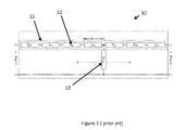
- the impedance of the source or the load may vary over time, thereby requiring the impedance matching network to be tunable so as to ensure the efficient transmission of power between the source and the load. This may be achieved by providing a tunable impedance network containing one or more tunable impedance sub-networks such as the one shown in figure 1 .
- the tunable impedance network 10 of figure 1 consists of a metal wire 11 and a slidable impedance element 13 that can be moved continuously up and down the wire 11. By sliding the impedance element Z TUNE 13 up and down the length of the wire 11, as indicated by the arrows, the impedance parameters seen at the two ports of the tunable impedance network 10 can be adjusted.
- Such a tunable impedance network is of course not suitable for integrated circuit solutions due the large area overhead required for its implementation and the need for manual control of the slidable impedance element 13.
- the same functionality can be approximated with a discrete set of switchable impedance elements in a switched capacitor array. By switching one of the elements, a capacitor can as it were be moved up and down along the wire.
- a switchable capacitor array as a conventional DAC, e.g. a thermometer-coded DAC, may provide a much larger tuning range.
- the maximum amount of capacitance that can then be connected to the wire is then n*C UNIT .
- the capacitance connected to the wire is influenced by routing inductance of the wire, which may, together with process variations, affect the precision of the switched capacitance, which is of crucial importance when the tunable impedance network is used for impedance balancing in electrical-balance duplexers.
- the basic concept is to create a so-called balance network impedance, the complex impedance value of which enables destructive signal interference at the receive output of a hybrid transformer.
- a tunable impedance network is provided.
- the tunable impedance network is provided with at least one variable impedance bank comprising a plurality of digitally controlled unit cells each connected from at least a first end to a routing wire in a parallel configuration and arranged when switched-on to adjust the impedance of the variable impedance bank by a discrete value.
- the unit cells may comprise a digitally controlled capacitor, which when activated adjusts the impedance of the variable impedance bank by its nominal value.
- the tunable impedance is provided with selection means comprising a plurality of predetermined digital control signals each corresponding to a desired impedance.
- the selection means are arranged for selecting based on the desired impedance the corresponding digital control signal to be supplied to the bank to switch-on a corresponding combination of said unit cells.
- the tunable impedance network is designed such that between each pair of unit cells in the bank a routing wire section is provided having a routing impedance, which contributes to the actual impedance generated by the variable impedance bank.
- Each of the predetermined control signals is provided for switching-on a combination of unit cells in such a way that the routing impedance of the routing wire section is exploited to fine-tune the actual impedance generated by the variable impedance bank.
- the actual impedance generated may be fine-tuned in the digital domain without the need for increasing the design complexity or increasing the area overhead of the impedance network.
- the actual impedance generated by the variable impedance bank may be fine-tuned without the need for providing additional components for this purpose, e.g. unit cells with a higher resolution to adjust the impedance of the variable impedance bank by a smaller discrete value, which may considerably increase the area overhead and design complexity of the tunable impedance network.
- variable impedance bank may negatively impact the tuning range of the actual impedance generated due to parasitics introduced in the layout of the unit cells. Therefore, by taking advantage of the routing impedance of the wire sections the actual impedance generated may be fine-tuned at a higher precision than the one defined strictly by the resolution of the unit cells in the variable impedance bank, without the need for providing unit cells having a higher resolution.
- each predetermined control signal may be provided for exploiting the impedance of the routing wire section to improve the precision of the actual impedance generated by the variable impedance bank.
- each desired impedance a control signal to switch-on a combination of unit cells, which are connected to one another by routing sections, each having a predetermined routing impedance, which when combined with the impedance adjustments effected by each switched-on unit cell generate an actual impedance that more closely matches the desired impedance.
- the impedance of the tunable impedance network may be tuned at a higher precision than the one defined strictly by the resolution of the unit cells in the variable impedance bank, without the need for providing unit cells having a higher resolution.
- the level of precision of the impedance generated may be further enhanced by giving at least some of the routing wire sections provided between each pair of unit cells a predetermined routing impedance. This may be achieved by means of a predetermined length of at least some of the routing wire sections, or by adding inductive components such as a loop to at least some of the routing wire sections.
- each predetermined control signal may be provided for exploiting the process variability of each unit cell so as to improve the precision of the actual impedance generated by the variable impedance bank. It has been found that by exploiting the process variability of the unit cells the precision of the actual impedance generated by the variable impedance bank may be adjusted in the digital domain rather providing unit cells of higher resolution for compensation, which would increase the design complexity and area overhead of the impedance network.
- control signals are in the form of a weighted coding scheme, such as a thermometer code.
- the variable impedance bank may be operated as a weight-coded Digital-to-Analogue Converter (DAC).
- DAC Digital-to-Analogue Converter
- each predetermined control signal may be provided for exploiting the impedance of the routing wire section to increase the resolution of the variable impedance bank. This can be achieved for example by designing the routing wire sections in such a way that their contribution to the overall impedance provides for a stepwise variation of the generated impedance at a granularity below that of the unit cells.
- the tunable impedance network is configured for operating in the RF frequency range, for example for impedance matching in an RF signal line.
- top, bottom, over, under and the like in the description and the claims are used for descriptive purposes and not necessarily for describing relative positions. The terms so used are interchangeable under appropriate circumstances and the embodiments of the disclosure described herein can operate in other orientations than described or illustrated herein.
- the tunable impedance network 10 of figure 1 may be realised in an integrated circuit by providing a variable impedance bank, an example of which is shown in figure 2 .
- the variable impedance bank 24 may be provided with an array of digitally controlled unit cells 23 each connected from at least a first end to a metal routing wire 11 and controlled by a control signal. Between each pair of unit cells 23 in the variable impedance bank 23 a routing wire section 22 is provided having a routing impedance, represented in figure 2 as a L wire , which contributes to the actual impedance generated by the variable impedance bank 24.
- Each of the unit cells 23 may comprise an impedance element, such as a capacitor, which when switched-on adjusts the impedance of the variable impedance bank 24.
- the impedance element may be operable between the on-state and off-state by means of a digital control signal supplied to a switch, e.g. a transistor, which is provided in series with the impedance element. Therefore, by providing different digital control signals the activated unit capacitances can be moved up and down the metal wire 21, i.e. a different combination can be selected, thereby adjusting the number of routing wire sections 22 that contribute to the actual impedance generated by the variable impedance bank 24. So this principle can be used to fine-tune the impedance of an impedance network 20.
- the variable impedance bank may be operated in a similar fashion as a Digital-to-Analogue Converter (DAC) comprising a number of unit cells arranged to be operated by a control signal supplied in the form of a thermometer code, or other coding/weighting schemes.
- DAC Digital-to-Analogue Converter
- the maximum impedance generated by the variable bank depends on the number of unit cells connected to the wire.
- Each of the unit cells in the variable impedance bank may be designed to have the same nominal value. For example, in the case where the unit cells comprise at least one digitally controlled capacitor, each unit cell may have the same nominal capacitance value.
- the variable impedance bank if desired, may also be designed so that there are sets of unit cells with a different nominal value.
- Figure 3 shows an example of how a variable impedance bank 24 of figure 2 may be operated as a thermometer-coded continuous-time DAC, for example a 3-bit variable impedance bank 34 comprising seven thermometer-coded unit cells 33.
- the cells which may be operated by applying a thermometer-coded control signal corresponding to a desired impedance value.
- a thermometer-coded control signal may be applied to the digitally controlled unit cells 33 asserting bits[0] to bit[2] so as to switch-on the corresponding combination of unit cells 33, while maintaining the remaining unit-cells 33 in the variable impedance bank 34 switched-off.
- the impedance of the routing section provided between each pair of unit cells contributes to the actual impedance generated by the variable impedance bank. Therefore, each time a different combination of unit-cells is switched-on the actual impedance generated may be different due to the different routing impedance of the wire sections connecting the switched-on unit cells.
- This may be achieved by providing to the variable impedance bank a control code that switches-on a predetermined combination of unit cells, which in combination with the routing impedance generate an actual impedance that closely matches the desired impedance.
- the routing impedance contributed by the routing wire section connecting each pair of unit cells, represented in figures 2 to 4 as L wire may be exploited to fine-tune the actual impedance generated by the variable impedance bank, for example when operated as a DAC.
- this may be achieved by providing for each desired impedance a predetermined control signal, which is each time provided for switching-on a corresponding combination of unit cells so as to generate, in combination with the routing impedance contributed by the routing sections, an actual impedance that is fine-tuned, for example more precise or even of higher resolution that the one provided by the nominal value of the unit cells of the variable impedance bank (see below).
- variable impedance bank By exploiting the impedance of the routing section connecting each pair of unit cells the actual impedance generated by the variable impedance bank may be fine-tuned in the digital domain without the need for providing unit cells of higher resolution, which would increase the design complexity and area overhead of the impedance network.
- Figure 4 shows an example of how the 3-bit variable impedance bank 34 of figure 3 may be operated so as to exploit the routing impedance of the routing wire section connecting each pair of unit cells to fine-tune the impedance of the tunable impedance network 30.
- the variable impedance bank 34 is operated in a similar function as a DAC comprising seven digitally controlled unit cells, arranged for receiving a control signal in the form of a thermometer code, or other coding/weighting schemes.
- a control code of 3 in the binary format, is coded in a conventional and logical way, with bits 0-2 asserted.
- a predetermined control signal may be selected to activate a corresponding combination of unit cells 33 that generate an actual impedance that more closely matches the desired impedance, thereby improving the precision of the actual impedance generated by the variable impedance bank 34.
- the natural process variability, caused due to the physical process spread and defects, in the matching of the unit cells may be exploited to fine-tune the actual impedance generated by the variable impedance bank 34. In the latter case, a calibration procedure would be applied to determine the most appropriate control signals.
- the level of fine-tuning of the actual impedance generated by the variable impedance bank may be controlled by means of the impedance of the routing wire section provided between each pair of unit cells.
- a predetermined impedance may be chosen, for example by choosing a predetermined length for at least some of the wire routing sections between pairs of cells. For example, by placing the unit cells in the physical layout at more or less compact spacing from each other, the level of the fine-tuning may be adjusted through the adjustment of the value of L wire .
- a compact physical layout may generate a smaller value for L wire , while a distributed physical layout may generate a larger value for L wire . In this way, the length of L wire can be used to set the minimum step precision that can be obtained by exploiting the routing impedance of the wire sections.
- inductive components may be applied in the routing wire sections, such as loops.
- the extent to which the precision of the actual impedance generated by the variable impedance bank can be adjusted depends on the thermometer code provided to the unit cells for generating a desired impedance. For example, in the 3-bit example of figure 4 , if the control code is equal to 0, i.e. all unit cells switched-off, or 7, e.g. all unit cells switched-on, there may be less freedom for adjustment. If the control code is equal to 1, i.e. one unit cell is switched-on, or 6, i.e. six unit cells switched-on, then the number of possible combinations of unit cells to realise the desired impedance value is equal to 8. If the control code is equal to 2, i.e. two unit cells switched-on, or 5, i.e.
- control codes near the mid-code will have the highest potential for precision enhancement.
- the digital control scheme can be orchestrated from the viewpoint of the entire tunable network.
- each of the predetermined control signals (unit cell combinations) corresponding to a desired impedance may be pre-selected.
- the selection of the predetermined digital control signals may be performed by means of a simulation or a calibration process effected prior or during the operation of the impedance network.
- the impedance network may further comprise selection means, for example a selector, comprising a plurality of predetermined digital control signals each corresponding to a desired impedance.
- the selector may be arranged for selecting based on the desired impedance the corresponding digital control signal to be supplied to the bank to switch-on a corresponding combination of said unit cells so that the impedance generated by the variable impedance bank more closely matches the desired impedance.
- the selector may iteratively use knowledge of the system's impedance network's governing equations and physical arrangement to iteratively tune to the desired actual impedance of the impedance bank in a deterministic way until the desired impedance value is reached. For example, the selector may itiratively go though the complete control code range or a portion of the control code range so as to "slide" each capacitor from left to right, one by one, until the desired value is achieved.
- Figure 5 shows an example of an impedance network 40 comprising a selector 42 arranged for providing to the variable impedance bank 34 a predetermined control signal based on desired impedance 41 received at a selector input.
- the selector 42 may be arranged for storing the predetermined control signals in a memory, e.g. a Look-up-Table (LUT), and arranged upon receiving a desired impedance value 41 at the input to select the corresponding control signal, which when applied to unit cells of the variable impedance bank 34 generates an impedance that matches the desired impedance received at the input of the selector 42 as close as possible.
- LUT Look-up-Table
- the selector 42 may be part of a closed loop control system that uses knowledge of the impedance network's governing equations and physical arrangement to iteratively tune the actual impedance of the impedance bank in a deterministic way until the desired impedance value is reached. Control steps using control feedback can be followed to systematically reach the desired control code.
- the selector 42 is thus arranged for providing to the variable impedance bank a number of control codes each arranged for switching-on a different combination of unit cells, and based on the actual impedance generated by the bank select the combination of unit cells that generates an actual impedance closely matching the desired impedance.
- the routing impedance of the wire sections connecting each pair of unit cells may be exploited to increase the resolution of the variable impedance bank. This may be achieved by providing a variable impedance bank operated as a DAC that has a resolution i.e. the smallest adjustment of impedance effected by the variable impedance bank to the tunable impedance network, at the same level as the fine-tuning step provided by the impedance of the routing wire sections.
- control code is only 3-bits
- the impedance generated with the impedance network may be tuned by "shifting" the active unit cells 53 along the routing wire 51.
- C TOT which is the sum of the capacitance generated by the switched-on unit cells, may be shifted along the routing wire 51 thereby enabling the generation of any integer multiple of L P , which is the routing inductance of the routing wire section 52 connecting each pair of unit cells 53.
- variable impedance bank 50 To exemplify the operation of the variable impedance bank 50, let's assume the simple case where all the digitally controlled capacitors 53 are switched-on in the variable impedance bank and are selected in a contiguous block that results in an effective capacitance C TOT , which includes all unwanted parasitics contributed among others from the routing wire sections 52 in that part of the variable impedance bank.
- C TOT represents the effective bank capacitance
- L p represents the routing parasitics leading from the RF signal line into the variable impedance bank.
- L p can be used to shift C TOT to become C TOT + C TOT /M, where M determines the desired granularity.
- M 2 ⁇ 5 would provide the extra precision required without requiring to increase the number of unit cells 53 in the variable impedance bank or to increase the resolution of each unit cell 53.
- the precision of the actual impedance generated by the variable impedance bank 50 may be improved from 8-bit to 10-bit, without the need for increasing the number of unit cells 53 or their respective resolution.
- the precision of the variable impedance bank may be improved by using the otherwise unwanted routing impedance of the wire sections provided between each pair of unit cells.
- the routing parasitic L p contributed by the routing wire section between the unit cells may be implemented in an integrated circuit using a metal wire having a predetermined length, e.g 50 micro-meters.
Landscapes
- Networks Using Active Elements (AREA)
- Semiconductor Integrated Circuits (AREA)
Priority Applications (4)
| Application Number | Priority Date | Filing Date | Title |
|---|---|---|---|
| EP14199406.1A EP3035529B1 (fr) | 2014-12-19 | 2014-12-19 | Réseau d'impédance accordable intégré |
| US14/971,597 US9979376B2 (en) | 2014-12-19 | 2015-12-16 | Integrated tunable impedance network |
| JP2015246295A JP6734047B2 (ja) | 2014-12-19 | 2015-12-17 | 集積化された調整可能なインピーダンス回路網 |
| US15/985,964 US20180302058A1 (en) | 2014-12-19 | 2018-05-22 | Integrated Tunable Impedance Network |
Applications Claiming Priority (1)
| Application Number | Priority Date | Filing Date | Title |
|---|---|---|---|
| EP14199406.1A EP3035529B1 (fr) | 2014-12-19 | 2014-12-19 | Réseau d'impédance accordable intégré |
Publications (2)
| Publication Number | Publication Date |
|---|---|
| EP3035529A1 true EP3035529A1 (fr) | 2016-06-22 |
| EP3035529B1 EP3035529B1 (fr) | 2019-07-17 |
Family
ID=52144490
Family Applications (1)
| Application Number | Title | Priority Date | Filing Date |
|---|---|---|---|
| EP14199406.1A Not-in-force EP3035529B1 (fr) | 2014-12-19 | 2014-12-19 | Réseau d'impédance accordable intégré |
Country Status (3)
| Country | Link |
|---|---|
| US (1) | US9979376B2 (fr) |
| EP (1) | EP3035529B1 (fr) |
| JP (1) | JP6734047B2 (fr) |
Families Citing this family (2)
| Publication number | Priority date | Publication date | Assignee | Title |
|---|---|---|---|---|
| WO2019217892A1 (fr) | 2018-05-10 | 2019-11-14 | Advanced Energy Industries, Inc. | Conversion numérique-analogique de précision en présence de contributions de bits fractionnaires variables et incertaines |
| JP7105183B2 (ja) * | 2018-12-27 | 2022-07-22 | 株式会社ダイヘン | インピーダンス整合装置及びインピーダンス整合方法 |
Citations (6)
| Publication number | Priority date | Publication date | Assignee | Title |
|---|---|---|---|---|
| US20040121745A1 (en) * | 2001-08-29 | 2004-06-24 | Meck Ronald A. | Method and apparatus for impedance matching in an amplifier using lumped and distributed inductance |
| US20090066443A1 (en) * | 2007-09-10 | 2009-03-12 | Ntt Docomo, Inc | Signal selecting device |
| US20090128386A1 (en) * | 2007-10-25 | 2009-05-21 | Stichting Imec Nederland | Analogue-to-digital converter and method for using the same |
| US20110043285A1 (en) * | 2009-08-19 | 2011-02-24 | Qualcomm Incorporated | Digital tunable inter-stage matching circuit |
| CN103337717A (zh) * | 2013-06-25 | 2013-10-02 | 华为技术有限公司 | 天线阻抗匹配装置、半导体芯片和方法 |
| US20140159987A1 (en) * | 2012-12-05 | 2014-06-12 | Thomson Licensing | Radio frequency device with compensation of permittivity dispersion of the substrate and adjustment method |
Family Cites Families (3)
| Publication number | Priority date | Publication date | Assignee | Title |
|---|---|---|---|---|
| US7468686B2 (en) * | 2007-02-06 | 2008-12-23 | Linear Technology Corporation | Systems and methods for providing compact digitally controlled trim of multi-segment circuits |
| JP2008227643A (ja) * | 2007-03-09 | 2008-09-25 | Matsushita Electric Ind Co Ltd | 平衡−不平衡変換回路 |
| US8963611B2 (en) * | 2009-06-19 | 2015-02-24 | Qualcomm Incorporated | Power and impedance measurement circuits for a wireless communication device |
-
2014
- 2014-12-19 EP EP14199406.1A patent/EP3035529B1/fr not_active Not-in-force
-
2015
- 2015-12-16 US US14/971,597 patent/US9979376B2/en not_active Expired - Fee Related
- 2015-12-17 JP JP2015246295A patent/JP6734047B2/ja not_active Expired - Fee Related
Patent Citations (7)
| Publication number | Priority date | Publication date | Assignee | Title |
|---|---|---|---|---|
| US20040121745A1 (en) * | 2001-08-29 | 2004-06-24 | Meck Ronald A. | Method and apparatus for impedance matching in an amplifier using lumped and distributed inductance |
| US20090066443A1 (en) * | 2007-09-10 | 2009-03-12 | Ntt Docomo, Inc | Signal selecting device |
| US20090128386A1 (en) * | 2007-10-25 | 2009-05-21 | Stichting Imec Nederland | Analogue-to-digital converter and method for using the same |
| US20110043285A1 (en) * | 2009-08-19 | 2011-02-24 | Qualcomm Incorporated | Digital tunable inter-stage matching circuit |
| US20140159987A1 (en) * | 2012-12-05 | 2014-06-12 | Thomson Licensing | Radio frequency device with compensation of permittivity dispersion of the substrate and adjustment method |
| CN103337717A (zh) * | 2013-06-25 | 2013-10-02 | 华为技术有限公司 | 天线阻抗匹配装置、半导体芯片和方法 |
| US20140375523A1 (en) * | 2013-06-25 | 2014-12-25 | Huawei Technologies Co., Ltd. | Antenna impedance matching apparatus, semiconductor chip, and method |
Also Published As
| Publication number | Publication date |
|---|---|
| EP3035529B1 (fr) | 2019-07-17 |
| US9979376B2 (en) | 2018-05-22 |
| JP6734047B2 (ja) | 2020-08-05 |
| JP2016119671A (ja) | 2016-06-30 |
| US20160182004A1 (en) | 2016-06-23 |
Similar Documents
| Publication | Publication Date | Title |
|---|---|---|
| JP7126529B2 (ja) | 位相スイッチト素子を使用したチューニング可能整合ネットワーク | |
| US9521023B2 (en) | Systems for analog phase shifting | |
| US8395459B2 (en) | Methods for tuning an adaptive impedance matching network with a look-up table | |
| KR101235048B1 (ko) | 개선된 적응형 임피던스 매칭을 위한 장치, 방법 및 기계 판독가능 저장매체 | |
| US9634823B1 (en) | Systems for integrated self-interference cancellation | |
| CN101689869A (zh) | 匹配天线的方法和装置 | |
| US10038415B2 (en) | Power amplifier matching circuit with DVCs | |
| JP2012518298A (ja) | 適応インピーダンス整合ネットワーク | |
| US20210159870A1 (en) | High Resolution Attenuator or Phase Shifter with Weighted Bits | |
| US20180302058A1 (en) | Integrated Tunable Impedance Network | |
| US10992334B2 (en) | Radio frequency switches with controllable resonant frequency | |
| KR20110037223A (ko) | 다중대역/다중모드 안테나의 임피던스 정합 장치 및 이를 이용한 안테나 | |
| EP3035529A1 (fr) | Réseau d'impédance accordable intégré | |
| EP3084958B1 (fr) | Ligne de charge accordable | |
| US11626893B2 (en) | Agile harmonic filtering | |
| US9634696B2 (en) | Transmitter for supporting multimode and multiband using multiple radio frequency (RF) digital-to-analog converters (DAC) and control method of the transmitter | |
| JP7376059B2 (ja) | スイッチ切り替え型可変容量、スイッチ切り替え型可変容量の設計方法、及びインピーダンス整合回路 | |
| KR20250089909A (ko) | 고주파수 위상천이기를 위한 장치 및 방법 | |
| JP6258270B2 (ja) | 適応インピーダンス整合ネットワーク | |
| US20130285762A1 (en) | Variable capacitor module |
Legal Events
| Date | Code | Title | Description |
|---|---|---|---|
| PUAI | Public reference made under article 153(3) epc to a published international application that has entered the european phase |
Free format text: ORIGINAL CODE: 0009012 |
|
| AK | Designated contracting states |
Kind code of ref document: A1 Designated state(s): AL AT BE BG CH CY CZ DE DK EE ES FI FR GB GR HR HU IE IS IT LI LT LU LV MC MK MT NL NO PL PT RO RS SE SI SK SM TR |
|
| AX | Request for extension of the european patent |
Extension state: BA ME |
|
| STAA | Information on the status of an ep patent application or granted ep patent |
Free format text: STATUS: REQUEST FOR EXAMINATION WAS MADE |
|
| 17P | Request for examination filed |
Effective date: 20161123 |
|
| RBV | Designated contracting states (corrected) |
Designated state(s): AL AT BE BG CH CY CZ DE DK EE ES FI FR GB GR HR HU IE IS IT LI LT LU LV MC MK MT NL NO PL PT RO RS SE SI SK SM TR |
|
| STAA | Information on the status of an ep patent application or granted ep patent |
Free format text: STATUS: EXAMINATION IS IN PROGRESS |
|
| 17Q | First examination report despatched |
Effective date: 20171027 |
|
| GRAP | Despatch of communication of intention to grant a patent |
Free format text: ORIGINAL CODE: EPIDOSNIGR1 |
|
| STAA | Information on the status of an ep patent application or granted ep patent |
Free format text: STATUS: GRANT OF PATENT IS INTENDED |
|
| RIC1 | Information provided on ipc code assigned before grant |
Ipc: H03H 7/38 20060101AFI20190130BHEP Ipc: H03H 7/40 20060101ALN20190130BHEP Ipc: H03M 1/80 20060101ALN20190130BHEP |
|
| INTG | Intention to grant announced |
Effective date: 20190304 |
|
| RIN1 | Information on inventor provided before grant (corrected) |
Inventor name: VAN LIEMPD, BAREND Inventor name: PORIS HERSHBERG, BENJAMIN |
|
| GRAS | Grant fee paid |
Free format text: ORIGINAL CODE: EPIDOSNIGR3 |
|
| GRAA | (expected) grant |
Free format text: ORIGINAL CODE: 0009210 |
|
| STAA | Information on the status of an ep patent application or granted ep patent |
Free format text: STATUS: THE PATENT HAS BEEN GRANTED |
|
| AK | Designated contracting states |
Kind code of ref document: B1 Designated state(s): AL AT BE BG CH CY CZ DE DK EE ES FI FR GB GR HR HU IE IS IT LI LT LU LV MC MK MT NL NO PL PT RO RS SE SI SK SM TR |
|
| REG | Reference to a national code |
Ref country code: GB Ref legal event code: FG4D |
|
| REG | Reference to a national code |
Ref country code: CH Ref legal event code: EP |
|
| REG | Reference to a national code |
Ref country code: DE Ref legal event code: R096 Ref document number: 602014050083 Country of ref document: DE |
|
| REG | Reference to a national code |
Ref country code: IE Ref legal event code: FG4D |
|
| REG | Reference to a national code |
Ref country code: AT Ref legal event code: REF Ref document number: 1156750 Country of ref document: AT Kind code of ref document: T Effective date: 20190815 |
|
| REG | Reference to a national code |
Ref country code: NL Ref legal event code: MP Effective date: 20190717 |
|
| REG | Reference to a national code |
Ref country code: LT Ref legal event code: MG4D |
|
| REG | Reference to a national code |
Ref country code: AT Ref legal event code: MK05 Ref document number: 1156750 Country of ref document: AT Kind code of ref document: T Effective date: 20190717 |
|
| PG25 | Lapsed in a contracting state [announced via postgrant information from national office to epo] |
Ref country code: FI Free format text: LAPSE BECAUSE OF FAILURE TO SUBMIT A TRANSLATION OF THE DESCRIPTION OR TO PAY THE FEE WITHIN THE PRESCRIBED TIME-LIMIT Effective date: 20190717 Ref country code: PT Free format text: LAPSE BECAUSE OF FAILURE TO SUBMIT A TRANSLATION OF THE DESCRIPTION OR TO PAY THE FEE WITHIN THE PRESCRIBED TIME-LIMIT Effective date: 20191118 Ref country code: HR Free format text: LAPSE BECAUSE OF FAILURE TO SUBMIT A TRANSLATION OF THE DESCRIPTION OR TO PAY THE FEE WITHIN THE PRESCRIBED TIME-LIMIT Effective date: 20190717 Ref country code: NL Free format text: LAPSE BECAUSE OF FAILURE TO SUBMIT A TRANSLATION OF THE DESCRIPTION OR TO PAY THE FEE WITHIN THE PRESCRIBED TIME-LIMIT Effective date: 20190717 Ref country code: SE Free format text: LAPSE BECAUSE OF FAILURE TO SUBMIT A TRANSLATION OF THE DESCRIPTION OR TO PAY THE FEE WITHIN THE PRESCRIBED TIME-LIMIT Effective date: 20190717 Ref country code: BG Free format text: LAPSE BECAUSE OF FAILURE TO SUBMIT A TRANSLATION OF THE DESCRIPTION OR TO PAY THE FEE WITHIN THE PRESCRIBED TIME-LIMIT Effective date: 20191017 Ref country code: LT Free format text: LAPSE BECAUSE OF FAILURE TO SUBMIT A TRANSLATION OF THE DESCRIPTION OR TO PAY THE FEE WITHIN THE PRESCRIBED TIME-LIMIT Effective date: 20190717 Ref country code: NO Free format text: LAPSE BECAUSE OF FAILURE TO SUBMIT A TRANSLATION OF THE DESCRIPTION OR TO PAY THE FEE WITHIN THE PRESCRIBED TIME-LIMIT Effective date: 20191017 Ref country code: AT Free format text: LAPSE BECAUSE OF FAILURE TO SUBMIT A TRANSLATION OF THE DESCRIPTION OR TO PAY THE FEE WITHIN THE PRESCRIBED TIME-LIMIT Effective date: 20190717 |
|
| PG25 | Lapsed in a contracting state [announced via postgrant information from national office to epo] |
Ref country code: ES Free format text: LAPSE BECAUSE OF FAILURE TO SUBMIT A TRANSLATION OF THE DESCRIPTION OR TO PAY THE FEE WITHIN THE PRESCRIBED TIME-LIMIT Effective date: 20190717 Ref country code: IS Free format text: LAPSE BECAUSE OF FAILURE TO SUBMIT A TRANSLATION OF THE DESCRIPTION OR TO PAY THE FEE WITHIN THE PRESCRIBED TIME-LIMIT Effective date: 20191117 Ref country code: LV Free format text: LAPSE BECAUSE OF FAILURE TO SUBMIT A TRANSLATION OF THE DESCRIPTION OR TO PAY THE FEE WITHIN THE PRESCRIBED TIME-LIMIT Effective date: 20190717 Ref country code: AL Free format text: LAPSE BECAUSE OF FAILURE TO SUBMIT A TRANSLATION OF THE DESCRIPTION OR TO PAY THE FEE WITHIN THE PRESCRIBED TIME-LIMIT Effective date: 20190717 Ref country code: GR Free format text: LAPSE BECAUSE OF FAILURE TO SUBMIT A TRANSLATION OF THE DESCRIPTION OR TO PAY THE FEE WITHIN THE PRESCRIBED TIME-LIMIT Effective date: 20191018 Ref country code: RS Free format text: LAPSE BECAUSE OF FAILURE TO SUBMIT A TRANSLATION OF THE DESCRIPTION OR TO PAY THE FEE WITHIN THE PRESCRIBED TIME-LIMIT Effective date: 20190717 |
|
| PG25 | Lapsed in a contracting state [announced via postgrant information from national office to epo] |
Ref country code: TR Free format text: LAPSE BECAUSE OF FAILURE TO SUBMIT A TRANSLATION OF THE DESCRIPTION OR TO PAY THE FEE WITHIN THE PRESCRIBED TIME-LIMIT Effective date: 20190717 |
|
| PG25 | Lapsed in a contracting state [announced via postgrant information from national office to epo] |
Ref country code: RO Free format text: LAPSE BECAUSE OF FAILURE TO SUBMIT A TRANSLATION OF THE DESCRIPTION OR TO PAY THE FEE WITHIN THE PRESCRIBED TIME-LIMIT Effective date: 20190717 Ref country code: IT Free format text: LAPSE BECAUSE OF FAILURE TO SUBMIT A TRANSLATION OF THE DESCRIPTION OR TO PAY THE FEE WITHIN THE PRESCRIBED TIME-LIMIT Effective date: 20190717 Ref country code: EE Free format text: LAPSE BECAUSE OF FAILURE TO SUBMIT A TRANSLATION OF THE DESCRIPTION OR TO PAY THE FEE WITHIN THE PRESCRIBED TIME-LIMIT Effective date: 20190717 Ref country code: PL Free format text: LAPSE BECAUSE OF FAILURE TO SUBMIT A TRANSLATION OF THE DESCRIPTION OR TO PAY THE FEE WITHIN THE PRESCRIBED TIME-LIMIT Effective date: 20190717 Ref country code: DK Free format text: LAPSE BECAUSE OF FAILURE TO SUBMIT A TRANSLATION OF THE DESCRIPTION OR TO PAY THE FEE WITHIN THE PRESCRIBED TIME-LIMIT Effective date: 20190717 |
|
| PG25 | Lapsed in a contracting state [announced via postgrant information from national office to epo] |
Ref country code: CZ Free format text: LAPSE BECAUSE OF FAILURE TO SUBMIT A TRANSLATION OF THE DESCRIPTION OR TO PAY THE FEE WITHIN THE PRESCRIBED TIME-LIMIT Effective date: 20190717 Ref country code: SK Free format text: LAPSE BECAUSE OF FAILURE TO SUBMIT A TRANSLATION OF THE DESCRIPTION OR TO PAY THE FEE WITHIN THE PRESCRIBED TIME-LIMIT Effective date: 20190717 Ref country code: IS Free format text: LAPSE BECAUSE OF FAILURE TO SUBMIT A TRANSLATION OF THE DESCRIPTION OR TO PAY THE FEE WITHIN THE PRESCRIBED TIME-LIMIT Effective date: 20200224 Ref country code: SM Free format text: LAPSE BECAUSE OF FAILURE TO SUBMIT A TRANSLATION OF THE DESCRIPTION OR TO PAY THE FEE WITHIN THE PRESCRIBED TIME-LIMIT Effective date: 20190717 |
|
| REG | Reference to a national code |
Ref country code: DE Ref legal event code: R097 Ref document number: 602014050083 Country of ref document: DE |
|
| PLBE | No opposition filed within time limit |
Free format text: ORIGINAL CODE: 0009261 |
|
| STAA | Information on the status of an ep patent application or granted ep patent |
Free format text: STATUS: NO OPPOSITION FILED WITHIN TIME LIMIT |
|
| PG2D | Information on lapse in contracting state deleted |
Ref country code: IS |
|
| REG | Reference to a national code |
Ref country code: CH Ref legal event code: PL |
|
| 26N | No opposition filed |
Effective date: 20200603 |
|
| REG | Reference to a national code |
Ref country code: BE Ref legal event code: MM Effective date: 20191231 |
|
| PG25 | Lapsed in a contracting state [announced via postgrant information from national office to epo] |
Ref country code: MC Free format text: LAPSE BECAUSE OF FAILURE TO SUBMIT A TRANSLATION OF THE DESCRIPTION OR TO PAY THE FEE WITHIN THE PRESCRIBED TIME-LIMIT Effective date: 20190717 Ref country code: SI Free format text: LAPSE BECAUSE OF FAILURE TO SUBMIT A TRANSLATION OF THE DESCRIPTION OR TO PAY THE FEE WITHIN THE PRESCRIBED TIME-LIMIT Effective date: 20190717 |
|
| PG25 | Lapsed in a contracting state [announced via postgrant information from national office to epo] |
Ref country code: IE Free format text: LAPSE BECAUSE OF NON-PAYMENT OF DUE FEES Effective date: 20191219 Ref country code: LU Free format text: LAPSE BECAUSE OF NON-PAYMENT OF DUE FEES Effective date: 20191219 |
|
| PG25 | Lapsed in a contracting state [announced via postgrant information from national office to epo] |
Ref country code: BE Free format text: LAPSE BECAUSE OF NON-PAYMENT OF DUE FEES Effective date: 20191231 Ref country code: LI Free format text: LAPSE BECAUSE OF NON-PAYMENT OF DUE FEES Effective date: 20191231 Ref country code: CH Free format text: LAPSE BECAUSE OF NON-PAYMENT OF DUE FEES Effective date: 20191231 |
|
| PGFP | Annual fee paid to national office [announced via postgrant information from national office to epo] |
Ref country code: GB Payment date: 20201123 Year of fee payment: 7 Ref country code: FR Payment date: 20201120 Year of fee payment: 7 Ref country code: DE Payment date: 20201119 Year of fee payment: 7 |
|
| PG25 | Lapsed in a contracting state [announced via postgrant information from national office to epo] |
Ref country code: CY Free format text: LAPSE BECAUSE OF FAILURE TO SUBMIT A TRANSLATION OF THE DESCRIPTION OR TO PAY THE FEE WITHIN THE PRESCRIBED TIME-LIMIT Effective date: 20190717 |
|
| PG25 | Lapsed in a contracting state [announced via postgrant information from national office to epo] |
Ref country code: MT Free format text: LAPSE BECAUSE OF FAILURE TO SUBMIT A TRANSLATION OF THE DESCRIPTION OR TO PAY THE FEE WITHIN THE PRESCRIBED TIME-LIMIT Effective date: 20190717 Ref country code: HU Free format text: LAPSE BECAUSE OF FAILURE TO SUBMIT A TRANSLATION OF THE DESCRIPTION OR TO PAY THE FEE WITHIN THE PRESCRIBED TIME-LIMIT; INVALID AB INITIO Effective date: 20141219 |
|
| PG25 | Lapsed in a contracting state [announced via postgrant information from national office to epo] |
Ref country code: MK Free format text: LAPSE BECAUSE OF FAILURE TO SUBMIT A TRANSLATION OF THE DESCRIPTION OR TO PAY THE FEE WITHIN THE PRESCRIBED TIME-LIMIT Effective date: 20190717 |
|
| REG | Reference to a national code |
Ref country code: DE Ref legal event code: R119 Ref document number: 602014050083 Country of ref document: DE |
|
| GBPC | Gb: european patent ceased through non-payment of renewal fee |
Effective date: 20211219 |
|
| PG25 | Lapsed in a contracting state [announced via postgrant information from national office to epo] |
Ref country code: GB Free format text: LAPSE BECAUSE OF NON-PAYMENT OF DUE FEES Effective date: 20211219 Ref country code: DE Free format text: LAPSE BECAUSE OF NON-PAYMENT OF DUE FEES Effective date: 20220701 |
|
| PG25 | Lapsed in a contracting state [announced via postgrant information from national office to epo] |
Ref country code: FR Free format text: LAPSE BECAUSE OF NON-PAYMENT OF DUE FEES Effective date: 20211231 |