EP3035530B1 - Vergleichsschaltkreis einer spannung mit einer schwelle - Google Patents
Vergleichsschaltkreis einer spannung mit einer schwelle Download PDFInfo
- Publication number
- EP3035530B1 EP3035530B1 EP15199659.2A EP15199659A EP3035530B1 EP 3035530 B1 EP3035530 B1 EP 3035530B1 EP 15199659 A EP15199659 A EP 15199659A EP 3035530 B1 EP3035530 B1 EP 3035530B1
- Authority
- EP
- European Patent Office
- Prior art keywords
- node
- circuit
- transistor
- voltage
- resistor
- Prior art date
- Legal status (The legal status is an assumption and is not a legal conclusion. Google has not performed a legal analysis and makes no representation as to the accuracy of the status listed.)
- Active
Links
Images


Classifications
-
- G—PHYSICS
- G01—MEASURING; TESTING
- G01R—MEASURING ELECTRIC VARIABLES; MEASURING MAGNETIC VARIABLES
- G01R19/00—Arrangements for measuring currents or voltages or for indicating presence or sign thereof
- G01R19/165—Indicating that current or voltage is either above or below a predetermined value or within or outside a predetermined range of values
- G01R19/16533—Indicating that current or voltage is either above or below a predetermined value or within or outside a predetermined range of values characterised by the application
- G01R19/16538—Indicating that current or voltage is either above or below a predetermined value or within or outside a predetermined range of values characterised by the application in AC or DC supplies
-
- H—ELECTRICITY
- H02—GENERATION; CONVERSION OR DISTRIBUTION OF ELECTRIC POWER
- H02J—ELECTRIC POWER NETWORKS; CIRCUIT ARRANGEMENTS OR SYSTEMS FOR SUPPLYING OR DISTRIBUTING ELECTRIC POWER; SYSTEMS FOR STORING ELECTRIC ENERGY
- H02J7/00—Circuit arrangements for charging or discharging batteries or for supplying loads from batteries
- H02J7/34—Parallel operation in networks using both storage and other DC sources, e.g. providing buffering
- H02J7/345—Parallel operation in networks using both storage and other DC sources, e.g. providing buffering using capacitors as storage or buffering devices
-
- G—PHYSICS
- G01—MEASURING; TESTING
- G01R—MEASURING ELECTRIC VARIABLES; MEASURING MAGNETIC VARIABLES
- G01R19/00—Arrangements for measuring currents or voltages or for indicating presence or sign thereof
- G01R19/0084—Measuring voltage only
-
- G—PHYSICS
- G01—MEASURING; TESTING
- G01R—MEASURING ELECTRIC VARIABLES; MEASURING MAGNETIC VARIABLES
- G01R19/00—Arrangements for measuring currents or voltages or for indicating presence or sign thereof
- G01R19/165—Indicating that current or voltage is either above or below a predetermined value or within or outside a predetermined range of values
- G01R19/16566—Circuits and arrangements for comparing voltage or current with one or several thresholds and for indicating the result not covered by subgroups G01R19/16504, G01R19/16528, G01R19/16533
- G01R19/16576—Circuits and arrangements for comparing voltage or current with one or several thresholds and for indicating the result not covered by subgroups G01R19/16504, G01R19/16528, G01R19/16533 comparing DC or AC voltage with one threshold
-
- H—ELECTRICITY
- H02—GENERATION; CONVERSION OR DISTRIBUTION OF ELECTRIC POWER
- H02M—APPARATUS FOR CONVERSION BETWEEN AC AND AC, BETWEEN AC AND DC, OR BETWEEN DC AND DC, AND FOR USE WITH MAINS OR SIMILAR POWER SUPPLY SYSTEMS; CONVERSION OF DC OR AC INPUT POWER INTO SURGE OUTPUT POWER; CONTROL OR REGULATION THEREOF
- H02M3/00—Conversion of DC power input into DC power output
- H02M3/02—Conversion of DC power input into DC power output without intermediate conversion into AC
- H02M3/04—Conversion of DC power input into DC power output without intermediate conversion into AC by static converters
- H02M3/10—Conversion of DC power input into DC power output without intermediate conversion into AC by static converters using discharge tubes with control electrode or semiconductor devices with control electrode
- H02M3/145—Conversion of DC power input into DC power output without intermediate conversion into AC by static converters using discharge tubes with control electrode or semiconductor devices with control electrode using devices of a triode or transistor type requiring continuous application of a control signal
- H02M3/155—Conversion of DC power input into DC power output without intermediate conversion into AC by static converters using discharge tubes with control electrode or semiconductor devices with control electrode using devices of a triode or transistor type requiring continuous application of a control signal using semiconductor devices only
- H02M3/156—Conversion of DC power input into DC power output without intermediate conversion into AC by static converters using discharge tubes with control electrode or semiconductor devices with control electrode using devices of a triode or transistor type requiring continuous application of a control signal using semiconductor devices only with automatic control of output voltage or current, e.g. switching regulators
-
- H—ELECTRICITY
- H02—GENERATION; CONVERSION OR DISTRIBUTION OF ELECTRIC POWER
- H02N—ELECTRIC MACHINES NOT OTHERWISE PROVIDED FOR
- H02N2/00—Electric machines in general using piezoelectric effect, electrostriction or magnetostriction
- H02N2/18—Electric machines in general using piezoelectric effect, electrostriction or magnetostriction producing electrical output from mechanical input, e.g. generators
- H02N2/181—Circuits; Control arrangements or methods
-
- H—ELECTRICITY
- H03—ELECTRONIC CIRCUITRY
- H03K—PULSE TECHNIQUE
- H03K17/00—Electronic switching or gating, i.e. not by contact-making and –breaking
- H03K17/30—Modifications for providing a predetermined threshold before switching
- H03K17/302—Modifications for providing a predetermined threshold before switching in field-effect transistor switches
-
- H—ELECTRICITY
- H03—ELECTRONIC CIRCUITRY
- H03K—PULSE TECHNIQUE
- H03K3/00—Circuits for generating electric pulses; Monostable, bistable or multistable circuits
- H03K3/02—Generators characterised by the type of circuit or by the means used for producing pulses
- H03K3/021—Generators characterised by the type of circuit or by the means used for producing pulses by the use, as active elements, of more than one type of element or means, e.g. BIMOS, composite devices such as IGBT
-
- H—ELECTRICITY
- H03—ELECTRONIC CIRCUITRY
- H03K—PULSE TECHNIQUE
- H03K3/00—Circuits for generating electric pulses; Monostable, bistable or multistable circuits
- H03K3/02—Generators characterised by the type of circuit or by the means used for producing pulses
- H03K3/26—Generators characterised by the type of circuit or by the means used for producing pulses by the use, as active elements, of bipolar transistors with internal or external positive feedback
- H03K3/28—Generators characterised by the type of circuit or by the means used for producing pulses by the use, as active elements, of bipolar transistors with internal or external positive feedback using means other than a transformer for feedback
- H03K3/281—Generators characterised by the type of circuit or by the means used for producing pulses by the use, as active elements, of bipolar transistors with internal or external positive feedback using means other than a transformer for feedback using at least two transistors so coupled that the input of one is derived from the output of another, e.g. multivibrator
- H03K3/286—Generators characterised by the type of circuit or by the means used for producing pulses by the use, as active elements, of bipolar transistors with internal or external positive feedback using means other than a transformer for feedback using at least two transistors so coupled that the input of one is derived from the output of another, e.g. multivibrator bistable
- H03K3/2893—Bistables with hysteresis, e.g. Schmitt trigger
-
- H—ELECTRICITY
- H03—ELECTRONIC CIRCUITRY
- H03K—PULSE TECHNIQUE
- H03K3/00—Circuits for generating electric pulses; Monostable, bistable or multistable circuits
- H03K3/02—Generators characterised by the type of circuit or by the means used for producing pulses
- H03K3/353—Generators characterised by the type of circuit or by the means used for producing pulses by the use, as active elements, of field-effect transistors with internal or external positive feedback
- H03K3/356—Bistable circuits
- H03K3/3565—Bistables with hysteresis, e.g. Schmitt trigger
-
- G—PHYSICS
- G01—MEASURING; TESTING
- G01R—MEASURING ELECTRIC VARIABLES; MEASURING MAGNETIC VARIABLES
- G01R19/00—Arrangements for measuring currents or voltages or for indicating presence or sign thereof
- G01R19/165—Indicating that current or voltage is either above or below a predetermined value or within or outside a predetermined range of values
- G01R19/16504—Indicating that current or voltage is either above or below a predetermined value or within or outside a predetermined range of values characterised by the components employed
- G01R19/16519—Indicating that current or voltage is either above or below a predetermined value or within or outside a predetermined range of values characterised by the components employed using FET's
-
- H—ELECTRICITY
- H02—GENERATION; CONVERSION OR DISTRIBUTION OF ELECTRIC POWER
- H02M—APPARATUS FOR CONVERSION BETWEEN AC AND AC, BETWEEN AC AND DC, OR BETWEEN DC AND DC, AND FOR USE WITH MAINS OR SIMILAR POWER SUPPLY SYSTEMS; CONVERSION OF DC OR AC INPUT POWER INTO SURGE OUTPUT POWER; CONTROL OR REGULATION THEREOF
- H02M1/00—Details of apparatus for conversion
- H02M1/0003—Details of control, feedback or regulation circuits
- H02M1/0016—Control circuits providing compensation of output voltage deviations using feedforward of disturbance parameters
- H02M1/0022—Control circuits providing compensation of output voltage deviations using feedforward of disturbance parameters the disturbance parameters being input voltage fluctuations
-
- H—ELECTRICITY
- H03—ELECTRONIC CIRCUITRY
- H03K—PULSE TECHNIQUE
- H03K2217/00—Indexing scheme related to electronic switching or gating, i.e. not by contact-making or -breaking covered by H03K17/00
- H03K2217/0036—Means reducing energy consumption
Definitions
- the present application relates to electronic circuits in general, and more particularly to a circuit for comparing a voltage to a threshold. It is aimed in particular at a circuit with reduced consumption, which can notably be used in a generator with ambient energy recovery. It also relates to an ambient energy recovery generator comprising such a circuit.
- Such a generator typically comprises an element for converting ambient energy into electricity, for example a piezoelectric element, and an electrical energy conversion circuit placed downstream of the ambient energy conversion element into electricity, adapted transforming the electrical energy supplied by the conversion element into electrical energy that can be exploited by an electronic system.
- the electrical energy conversion circuit may include a circuit adapted to compare an input voltage to a threshold, and provide a power supply to a load when the input voltage exceeds that threshold.
- circuit adapted to compare an input voltage to a threshold and to supply a supply voltage to a load when the input voltage exceeds the threshold, this circuit does not require power supply. other than the input voltage for its operation.
- a circuit is disclosed for example in the document US 7,105.98 .
- An object of an embodiment is to provide such a circuit according to claims 1 to 8, having a reduced power consumption compared to existing circuits.
- An object of an embodiment is to provide an ambient energy recovery generator according to claims 9 to 14, including such a circuit.
- an embodiment provides a circuit for comparing a voltage at a threshold, comprising: first and second nodes for applying said voltage; a first branch having a first transistor in series with a first resistance between the first and second nodes; a second branch parallel to the first branch, having second and third series resistors forming a voltage divider bridge between the first and second nodes, the midpoint of the divider bridge being connected to a control node of the first transistor; and a third branch comprising a second transistor in series with a resistive and / or capacitive element, between the control node of the first transistor and the first or second node, a control node of the second transistor being connected to the midpoint of the association in series of the first transistor and the first resistor.
- the midpoint of the series association of the second transistor and the element resistive and / or capacitive, and the application node of said voltage not connected to the third branch constitute nodes for supplying an output voltage of the circuit, intended to be connected to a load to be powered.
- the circuit further comprises: between the middle point of the series association of the second transistor and the resistive and / or capacitive element, and the application node of said voltage not connected to the third branch, a fourth resistance; and between the application node of said voltage not connected to the third branch and a third node, a third transistor having a control node connected to the midpoint of the series connection of the second transistor and the resistive element and or capacitive, in which the application node of said voltage connected to the third branch, and the third node, constitute nodes for supplying an output voltage of the circuit, intended to be connected to a load to be powered.
- the first transistor is an NPN bipolar transistor or an N-channel MOS transistor
- the second transistor is a P-channel MOS transistor or a PNP bipolar transistor
- the first resistor is on the first node side and the first transistor is on the second node side
- the third branch is between the control node of the first transistor and the first node.
- the first transistor is a PNP bipolar transistor or a P-channel MOS transistor
- the second transistor is an N-channel MOS transistor or an NPN bipolar transistor
- the first resistor is on the second node side and the first transistor is on the first node side
- the third branch is between the control node of the first transistor and the second node.
- the resistive and / or capacitive element is a resistor.
- the resistive and / or capacitive element is an RC cell comprising a resistor and a capacitor.
- At least one of the second and third resistors is a thermistor or a combination of one or more resistors and one or more thermistors.
- an ambient energy recovery generator comprising: an element for converting ambient energy into electrical energy; a first capacitor adapted to store charges generated by said conversion element; and a first comparison circuit of the aforementioned type, the first capacitor being connected between the first and second nodes of the first comparison circuit.
- the generator further comprises an inductive loading circuit of a second capacitor from the input voltage and the first comparison circuit.
- the inductive charging circuit is a voltage-reducing circuit.
- the inductive charging circuit is a voltage booster circuit.
- the generator further comprises a second comparison circuit of the aforementioned type, the second capacitor being connected between the first and second nodes of the second comparison circuit.
- the same elements have been designated with the same references in the various figures.
- the terms “approximately”, “substantially”, “about”, “in the order of”, etc. mean “to within 20%”, or, where it is a zero voltage, “between -300 and 300 mV", or, in the case of a zero current, "between -50 and 50 nA”.
- the term “connected” will be used to designate a direct electrical connection, without intermediate electronic component, for example by means of a conductive track, and the term “coupled” or the term “connected”, to designate either a direct electrical connection (meaning “connected”) or a connection via one or more intermediate components (resistor, capacitor, etc.).
- the figure 1 is an electrical diagram illustrating an example of an embodiment of a circuit for comparing an input voltage Ve with a threshold.
- the comparison circuit 100 of the figure 1 comprises a first branch comprising a resistor R1 and a transistor T1 in series between nodes A and B for applying the voltage Ve. More particularly, in the example shown, the resistor R1 has a first end connected to the node A and a second end connected to a node C, and the transistor T1 has a first conduction node connected to the node C and a second conduction node connected to the node B.
- the transistor T1 is a bipolar transistor NPN type whose collector (c) is connected to the node C and whose emitter (e) is connected to the node B.
- the circuit 100 further comprises a second branch parallel to the first branch, comprising two resistors R2 and R3 in series between the nodes A and B. More particularly, in the example shown, the resistor R2 has a first end connected to the node A and a second end connected to a node D, and the resistor R3 has a first end connected to the node D and a second end connected to the node B.
- the resistors R2 and R3 form a voltage divider bridge.
- the node D, or midpoint of the divider bridge is connected to a control node of the transistor T1, namely the base (b) of the transistor T1 in the example shown.
- the circuit 100 further comprises a third branch, comprising a transistor T2 in series with a resistive element Rf, between the node A and the node D. More particularly, in the example shown, the resistor Rf has a first end connected to the node D and a second end connected to a node E, and the transistor T2 has a first conduction node connected to the node E and a second conduction node connected to the node A.
- the transistor T2 is a MOS transistor to channel P whose source (s) is connected to the node A and whose drain (d) is connected to the node E.
- a control node of the transistor T2, its gate (g) in this example, is connected to the node C.
- the input voltage Ve may be a DC voltage supplied by a source of electrical energy (not shown), for example the voltage across a capacitor for collecting electric charges generated by an ambient energy conversion element. electricity.
- the nodes E and B are nodes for supplying an output voltage Vs of the circuit 100.
- An LD load to be powered for example a wireless sensor (temperature, humidity, brightness sensor, etc.), a light source using for example a light emitting diode or a set of light-emitting diodes, etc., is connected between the nodes E and B of the circuit 100.
- circuit 100 The operation of circuit 100 is as follows. When the input voltage Ve is low, the voltage across the resistor R3 of the divider bridge is not sufficient to turn on the transistor T1. The transistor T1 is blocked. The voltage across the resistor R1, corresponding to the gate-source voltage of the transistor T2 in this example, is then substantially zero. The transistor T2 is thus blocked. The current flowing through the load LD is then substantially zero, and the load LD is not powered. The output voltage Vs of the circuit 100 is then approximately zero.
- the resistive element Rf then contributes to lowering the potential of the node D by pulling it towards that of the node E (then substantially equal to that of the node B), and thus reinforcing the blocking of the transistor T1.
- the voltage across the resistor R3 reaches the turn-on threshold of the transistor T1.
- the transistor T1 then becomes conducting, and a current flows in the branch comprising the resistor R1 and the transistor T1.
- the voltage across the resistor R1, or source-gate voltage of the transistor T2 in this example then increases until the conduction threshold of the transistor T2 is reached.
- the transistor T2 therefore becomes him also passing.
- the load LD is then fed, and the output voltage Vs of the circuit 100 becomes substantially equal to the input voltage Ve (at the voltage drop of the transistor T2 near).
- the resistive element Rf then tends to enhance the potential of the node D by pulling it towards that of the node E (then substantially equal to that of the node A), and thus contributes to maintaining the transistor T1 in the on state.
- the thresholds V SH and V SB can be calculated as follows: V SH ⁇ von * 1 R 3 + 1 R 2 + 1 Rf 1 R 2 ; and V SB ⁇ von * 1 R 3 + 1 R 2 + 1 Rf 1 R 2 + 1 Rf .
- the values of the resistors R1, R2, R3 and Rf are preferably relatively high in order to limit the electrical consumption of the circuit 100.
- the resistor R1, the resistor R2 + R3 of the divider bridge, and the resistor Rf are greater than 5 M ⁇ , and preferably greater than 50 M ⁇ .
- the resistor R1 is about 10 M ⁇
- the resistor R2 is about 50 M ⁇
- the resistor R3 is about 7 M ⁇
- the resistor Rf is about 150 M ⁇ .
- the transistor T1 may be replaced by an N-channel MOS transistor whose source, drain and gate are respectively connected to the node B, the node C and the node D.
- the use of a bipolar transistor has the advantage, however, of improving the accuracy of the switching thresholds, insofar as the conduction voltage of a bipolar transistor is generally less sensitive to temperature variations and to manufacturing variations than that of a MOS transistor. .
- the transistor T2 can be replaced by a PNP bipolar transistor whose emitter, collector and base are respectively connected to the node A, the node E and the node C.
- MOS transistor presents however the advantage of limiting the consumption of the circuit 100, a bipolar transistor in fact consuming a basic current in the on state.
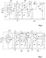
- the figure 2 is an electrical diagram illustrating an alternative embodiment of a comparison circuit of an input voltage Ve to a threshold.
- the comparison circuit 200 of the figure 2 substantially comprises the same elements as the circuit 100 of the figure 1 , and differs from circuit 100 from figure 1 essentially in that the conductivity types of the transistors T1 and T2 are reversed, in that the positions of the transistor T1 and the resistor R1 are inverted, in that the positions of the resistors R2 and R3 are inverted, and that the Transistor T2 and Load LD positions are inverted.
- the nodes conduction of the transistor T1 are connected to the nodes A and C
- the ends of the resistor R1 are connected to the nodes C and B
- the ends of the resistor R2 are connected to the nodes D and B
- the ends of the resistor R3 are connected to the nodes D and A
- the conduction nodes of the transistor T2 are connected to the nodes E and B
- the ends of the resistor Rf are connected to the nodes D and E
- the control node of the transistor T1 is connected to the node D
- the node of transistor T2 control is connected to the node C
- the load LD is connected between the nodes A and E, which constitute the supply nodes of the output voltage Vs of the circuit 200.
- the input voltage Ve is applied between the nodes A and B.
- the transistor T1 is a PNP bipolar transistor whose emitter (e) is connected to the node A, whose collector (c) is connected to the node C and whose base (b) is connected to the node D, and the transistor T2 is an N-channel MOS transistor whose source (s) is connected to the node B, whose drain (d) is connected to the node E, and whose gate (g) is connected to the node C .
- circuit 200 of the figure 2 is the next.
- the voltage across the resistor R3 of the divider bridge is not sufficient to turn on the transistor T1.
- the transistor T1 is blocked.
- the voltage across the resistor R1, corresponding to the gate-source voltage of the transistor T2 in this example, is then substantially zero.
- the transistor T2 is thus blocked.
- the current flowing through the load LD is then substantially zero, and the load LD is not powered.
- the output voltage Vs of the circuit 200 is then approximately zero.
- the resistive element Rf contributes to raising the potential of the node D by pulling it towards that of the node E (then substantially equal to that of the node A), and thus reinforces the blocking of the transistor T1.
- the voltage across the resistor R3 reaches the threshold conduction of transistor T1.
- the transistor T1 then becomes conducting, and a current flows in the branch comprising the resistor R1 and the transistor T1.
- the voltage across the resistor R1, or gate-source voltage of the transistor T2 in this example then increases until the conduction threshold of the transistor T2 is reached.
- the transistor T2 thus becomes also passing.
- the load LD is then fed and the output voltage Vs of the circuit 200 then becomes substantially equal to the input voltage Ve (at the voltage drop of the transistor T2 near).
- the resistive element Rf then tends to lower the potential of the node D by pulling it towards that of the node E (then substantially equal to that of the node B), and thus contributes to maintaining the transistor T1 in the on state.
- the circuit 200 has a function identical or similar to that of the circuit 100 of the figure 1 , and has, like the circuit 100, a hysteresis operation, the high switching thresholds V SH and low V SB of the circuit being able to be calculated by the formulas mentioned above in connection with the example of the figure 1 (Von designating, as in the example of the figure 1 , the voltage to be applied across the resistor R3 to make the transistor T1 conductive).
- the transistor T1 of the circuit 200 may be replaced by a P-channel MOS transistor whose source, drain and gate are respectively connected to the node A, the node C and the node D.
- a bipolar transistor however, as in the example of the figure 1 , the advantage of improving the accuracy of the switching thresholds V SH and V SB .
- the transistor T2 of the circuit 200 can be replaced by a bipolar transistor of the NPN type whose emitter, collector and base are respectively connected to the node B, the node E and the node C.
- the use of a MOS transistor has the advantage of reducing the power consumption of the circuit 200.
- the figure 3 is an electrical diagram illustrating another variant embodiment of a circuit for comparing an input voltage Ve with a threshold.
- the comparison circuit 300 of the figure 3 includes the same elements as circuit 200 of the figure 2 , arranged substantially in the same manner as in the example of figure 2 , and differs from circuit 200 from figure 2 in that it further comprises a resistor R4 whose ends are respectively connected to the nodes A and E, and a transistor T3 whose conduction nodes are respectively connected to the node A and to a node F, and whose control node is connected to the node E.
- the resistor R4 preferably has a value lower than the resistance Rf, for example between 5% and 20% of the value of the resistor Rf, for example of the order of 10% of the value of the resistor Rf, so to enable the blocking of the transistor T3 when the transistor T2 is off.
- the transistor T3 is a P-channel MOS transistor whose source is connected to the node A, whose drain is connected to the node F, and whose gate is connected to the node E.
- the input voltage Ve is applied between the nodes A and B.
- the load LD is connected between the nodes F and B, which constitute the supply nodes of the output voltage Vs of the circuit.
- circuit 300 The operation of circuit 300 is as follows. When the input voltage Ve is low, the voltage at the terminals of the R3 resistor of the divider bridge is not sufficient to turn on the transistor T1, which is blocked. The voltage across the resistor R1 is then substantially zero, which results in the transistor T2 being off. The voltage across the resistor R4 is then lower than the switching threshold of the transistor T3, and the transistor T3 is off. The load LD is then not powered, and the output voltage Vs of the circuit 300 is approximately zero.
- the resistive element Rf contributes to raising the potential of the node D by pulling it towards that of the node E (then substantially equal to that of the node A), and thus reinforces the blocking of the transistor T1.
- the resistive element Rf then tends to lower the potential of the node D by pulling it towards that of the node E (then substantially equal to that of the node B), and thus contributes to maintaining the transistor T1 in the on state.
- circuit 300 of the figure 3 present, as in the previous examples, a type of operation hysteresis, the switching thresholds V SH and V SB being the same as in the example of the figure 2 with the difference that the term Rf in the aforementioned calculation formula must be replaced by Rf + R4.
- the transistor T3 can be replaced by a PNP bipolar transistor, whose emitter is connected to the node A, whose collector is connected to the node F, and whose base is connected to the node E.
- a MOS transistor has the advantage of reducing the electrical consumption of the circuit 300.
- An advantage of the embodiment of the figure 3 is that the load LD has a power node connected to ground (node B), which provides a robust control, and avoid unwanted switching related parasitic transient signals.
- a complementary embodiment of the circuit 300 of the figure 3 can be performed by inverting the conductivity types of transistors T1, T2 and T3.
- This variant embodiment has not been shown and will not be detailed, but follows directly from the previous examples.
- this variant can be obtained by adding to the circuit 100 of the figure 1 a resistor R4 between the nodes E and B, and an N-channel MOS transistor or a NPN type bipolar transistor T3 between the node B and a node F, the control node of this transistor T3 being connected to the node E.
- the load LD is then connected between the nodes A and F, which constitute the nodes for supplying the output voltage Vs of the circuit.
- the figure 4 is an electrical diagram illustrating another variant embodiment of a circuit for comparing an input voltage Ve with a threshold.
- the comparison circuit 400 of the figure 4 comprises substantially the same elements as the circuit 200 of the figure 2 and differs from the circuit 200 essentially in that, in the circuit 400, the resistor Rf is replaced by a series association of a resistor Rf and a capacitor Cf connecting the nodes D and E. More particularly, in the example shown, the resistor Rf has a first end connected to the node D and a second end connected to a node G, and the capacitor Cf has a first electrode connected to the node G and a second electrode connected to the node E.
- the resistor Rf and the capacitor Cf can, however, be inverted. In other words, in the example of the figure 4 the resistance Rf is replaced by an RC cell.
- the output voltage Vs of the circuit 400 becomes substantially equal to the input voltage Ve (at the voltage drop of the transistor T2 near), and the load LD is fed .
- the falling edge of the voltage between the nodes E and B is transmitted to the node G by the capacitor Cf, which tends to lower the potential of the node D and thus contributes to maintaining the the on state of the transistor T1 as the capacitor Cf is not discharged.
- the circuit 400 remains on and feeds the load LD for a time ⁇ adjustable in particular by the value of the resistor Rf and by the value of the capacitor Cf.
- circuit 400 of the figure 4 does not have a hysteresis operation
- the presence of the RC cell between the nodes D and E makes it possible, by guaranteeing a minimum duration of supply of the load LD, to avoid an unwanted oscillation between the powered mode and the non-powered mode the load LD, especially in the case where switching from the off state to the on state is accompanied by a strong current draw in the LD load.
- the value of the resistor Rf is between 100 k ⁇ and 10 M ⁇ , for example of the order of 1 M ⁇ , and the capacity of the capacitor Cf is between 1 nF and 100 nF, for example of the order of 10 nF .
- the RC cell can be replaced by a single capacitor, or by a RC cell of another type, for example a parallel association of a resistor Rf and a capacitor Cf.
- a resistive element additional (not shown) and / or additional capacitive element (not shown) can be connected in parallel with the RC cell, between the nodes D and E.
- the variant embodiment of the figure 4 is compatible with all the examples of comparison circuits described above, that is to say that in each of the circuits described in connection with the Figures 1, 2 and 3 the resistor Rf may be replaced by an RC cell, or by a parallel association of an RC cell and a resistive element and / or a capacitive element.
- the comparison circuit may further comprise a discharge resistor, not shown, between the supply nodes of the output voltage Vs, in parallel with the load LD.
- a discharge resistor not shown, between the supply nodes of the output voltage Vs, in parallel with the load LD.
- the discharge resistor may have a value of between 10 k ⁇ and 5 M ⁇ , for example of the order of 100 k ⁇ .
- one and / or the other of the resistors R2 and R3 of the voltage divider bridge can be replaced by a thermistor, or by a series and / or parallel association comprising one or more resistors and one or more thermistors, chosen to compensate for the temperature drift of the voltage Von of conduction of the transistor T1 (so as to maintain the switching thresholds of the circuit substantially independent of the temperature).
- the figure 5 is an electrical diagram illustrating an example of an embodiment of an ambient energy recovery generator comprising a circuit for comparing a voltage at a threshold of the type described in relation to the Figures 1 to 4 .
- the generator of the figure 5 comprises an element 501 for converting ambient energy into electricity, for example a piezoelectric conversion element.
- the generator of the figure 5 further comprises a first circuit 510 for shaping the electrical energy produced by the element 501.
- the circuit 510 comprises a voltage rectifier circuit 512 and a capacitor Cb1 for storing the electrical energy produced by the element 501.
- the element 501 is connected between input nodes H and I of the rectifying circuit 512, which constitute nodes of input circuit 510, and the capacitor Cb1 is connected between output nodes J and K of the rectifier circuit 512, which constitute output nodes of the circuit 510.
- the rectifier circuit 512 is a bridge of diodes comprising a first branch of two diodes in series between the nodes K and J, and, in parallel with the first branch, a second branch of two diodes in series between the nodes K and J, the four diodes of the bridge having all the same direction of conductivity, namely that each diode has its node-side anode K and its node-side cathode J.
- the midpoint of the first branch is connected to the node H, and the middle point of the second branch is connected to node I.
- the generator of the figure 5 further comprises a circuit for comparing a voltage at a threshold of the type described in relation to the Figures 1 to 4 , circuit 400 of the figure 4 in this example.
- the output nodes J and K of the conversion circuit 510 are respectively connected to the input nodes A and B of the comparison circuit 400.
- the generator of the figure 5 further comprises, at the output of the comparison circuit 400, a circuit 520 for inductive charging of a second capacitor Cb2, of capacitance greater than that of the capacitor Cb1.
- the circuit 520 comprises input nodes L and M respectively connected to the output nodes A and E of the circuit 400, and output nodes N and O, the capacitor Cb2 being connected between the nodes N and O.
- the node O is connected to the node B of the comparison circuit 400.
- the circuit 520 is a voltage-reducing circuit (Buck converter type), that is to say that the voltage it delivers across the capacitor Cb2 is lower than the input voltage applied between the nodes L and O of the circuit 520.
- the circuit 520 comprises a resistor R5 whose first end is connected to the node L and a second end of which is connected to the node M, and a transistor T4 whose first conduction node is connected to the node L, a second conduction node of which is connected to a node P, and a control node of which is connected to the node M.
- the transistor T4 is a P-channel MOS transistor whose source (s) and drain (d) regions are respectively connected to the nodes L and P, and whose gate (g) is connected to the node M.
- the circuit 520 further comprises an inductance L1, a first end of which is connected to the node P and a second end of which is connected to the node N, and a diode D1, or freewheeling diode of the power circuit, whose anode is connected to the node O and whose cathode is connected to the node P.
- a load to be powered may be connected to the N and O output nodes of the circuit 520, which in this example constitute generator output nodes.
- the operation of the generator of the figure 5 is the next.
- the element 501 for converting ambient energy into electricity and the rectifying circuit 512 form a source of electrical energy delivering a current to the capacitance Cb1, causing the appearance of a voltage Ve across the capacitor Cb1, this voltage being itself applied to the input of the comparison circuit 400.
- the output voltage Vs of the circuit 400 becomes substantially equal to the input voltage Ve (at the voltage drop of the transistor T2 near), which causes the conduction of transistor T4.
- the circuit 400 then remains on for a time ⁇ adjustable in particular by the value of the resistor Rf and by the value of the capacitor Cf.
- the voltage Ve charges, through the inductor L1, the capacitor Cb2.
- the circuit 400 After the duration ⁇ , if the voltage Ve has fallen below the threshold V SH , the circuit 400 is blocked, and the voltage Vs is canceled until the voltage Ve rises above the threshold V SH . During the blocking period of the circuit 400, the freewheeling diode D1 ends up transferring in the capacitor Cb2 the residual energy present in the inductance L1.
- the generator of the figure 5 enables the capacitor Cb2 to be charged by means of the inductive circuit 520, from a capacitor Cb1 of smaller capacity.
- This arrangement makes it possible to avoid putting a capacitor of large capacity directly at the output of the conversion element 501, which would degrade the efficiency of the conversion element 501.
- the figure 6 is an electrical diagram illustrating an alternative embodiment of an ambient energy recovery generator comprising a circuit for comparing a voltage at a threshold of the type described in relation to the Figures 1 to 4 .
- the generator of the figure 6 differs from the generator of the figure 5 basically in that the voltage-lowering charging circuit 520 of the generator of the figure 5 has been replaced by a voltage boosting circuit 620 (Boost converter type).
- Boost converter type voltage boosting circuit 620
- the circuit 620 comprises, as in the example of the figure 5 , L and M input nodes respectively connected to the output nodes A and E of the comparison circuit 400, and N and O output nodes connected to the electrodes of a capacitor Cb2 of capacitance greater than that of the capacitor Cb1.
- the node O is connected to the node B of the comparison circuit 400.
- the circuit 620 comprises an inductor L1 whose first end is connected to the node L and whose second end is connected to the node M, and a diode D1 whose anode is connected to the node M and whose cathode is connected to the node N.
- a load to be powered may be connected to the N and O output nodes of the circuit 620, which in this example constitute generator output nodes.
- the operation of the generator of the figure 6 is identical or similar to that of the figure 5 with the difference that, in the example of figure 6 , the output voltage of the generator delivered across the capacitor Cb2 is greater than the voltage across the capacitor Cb1.
- the figure 7 is an electrical diagram illustrating another alternative embodiment of an ambient energy recovery generator comprising a circuit for comparing a voltage at a threshold of the type described in relation to the Figures 1 to 4 .
- the generator of the figure 7 includes the same elements as the generator of the figure 6 , arranged in substantially the same manner, and further comprises a second voltage comparison circuit 400 '.
- the circuit 400 ' is identical to the circuit 400, with component values that may be different, and all the elements of the circuit 400' have been designated on the figure 7 by the same references as those of the figure 4 , supplemented by the sign "'".
- the input nodes A 'and B' of the circuit 400 ' are respectively connected to the output nodes N and O of the circuit 620.
- a load LD to be powered is connected between the output nodes A' and E 'of the circuit 400'. which constitute the output nodes of the generator of the figure 7 .
- the load LD is supplied for a duration ⁇ ' by a voltage substantially equal to the voltage across the capacitor Cb2 (at the voltage drop of transistor T2 'near).
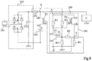
- the figure 8 is a circuit diagram of another alternative embodiment of an ambient energy recovery generator comprising a circuit for comparing a voltage at a threshold of the type described in relation to the Figures 1 to 4 .
- the generator of the figure 8 comprises an element 501 for converting ambient energy into electricity, and a circuit 510 for shaping the electrical energy produced by the element 501.
- These elements are for example identical to what has been described previously.
- the generator of the figure 8 further comprises a booster battery 801 for taking over for supplying a load C, for example a sensor or a light source, when the ambient energy converter into electricity does not provide enough electricity.
- the battery is connected in series with a diode D2 and a P-channel MOS transistor T5 between the output nodes J and K of the circuit 510 (in parallel with the capacitor Cb1). More particularly, in the example shown, the anode of the diode D2 is connected to the node J, the cathode of the diode D2 is connected to the drain of the transistor T5, the source of the transistor T5 is connected to the positive terminal (+) of the battery 801, and the negative (-) terminal of the battery 801 is connected to the node K.
- the generator of the figure 8 further comprises a circuit for comparing a voltage at a threshold of the type described in relation to the Figures 1 to 4 , circuit 100 of the figure 1 in this example.
- the output nodes J and K of the conversion circuit 510 are respectively connected to the input nodes A and B of the comparison circuit 100.
- the generator of the figure 8 further comprises, at the output of the comparison circuit 100, a resistor RL.
- the ends of the resistor RL are respectively connected to the output nodes E and B of the circuit 100.
- the node E is further connected (connected in the example shown) to the gate (g) of the transistor T5 .
- the charge C to be supplied has its positive and negative supply terminals respectively connected to the midpoint S between the diode D2 and the transistor T5, and to the node K.
- the voltage across the capacitor Cb1 is substantially zero, and the transistor T5 is conducting.
- the charge C is then powered only by the battery 801.
- the capacitor Cb1 is charged.
- the circuit 100 switches, which causes the transistor T5 to open.
- the charge C is then fed by the capacitor Cb1 via the diode D2. If the voltage across the capacitor Cb1 continues to increase, the conversion circuit 510 recharges the battery 801 via the intrinsic drain-source diode of the transistor 801, while continuing to supply the load C.
- the circuit 100 switches again, which causes the transistor T5 to be turned on.
- the charge C is then powered only by the battery 801, until the voltage across the capacitor Cb1 again reaches the high switching threshold of the hysteresis comparator.
- the voltage comparison circuits of the type described in relation to the Figures 1 to 4 may be used in applications other than ambient energy recovery generators.
- a circuit for comparing a voltage at a threshold of the type described in relation to the Figures 1 to 4 may be used to monitor the charge and / or discharge of a battery, for example to trigger an alarm or disconnect switch when a critical charge and / or discharge level is reached.
- the described embodiments are not limited to the particular examples of generator architectures described in connection with the Figures 5 to 7 .
- an ambient energy recovery generator may comprise only the upstream portion of the generator of the figure 5 , without the inductive charging circuit 520, a load to be powered can then be connected between the output nodes of the comparison circuit.
- the two voltage comparison circuits 400 and 400 ' may not be identical, but have different architectures, chosen from the architectures described in connection with the Figures 1 to 4 .
Landscapes
- Engineering & Computer Science (AREA)
- Power Engineering (AREA)
- Physics & Mathematics (AREA)
- General Physics & Mathematics (AREA)
- Dc-Dc Converters (AREA)
Claims (14)
- Eine Schaltung (100; 200; 300; 400) zum Vergleichen einer Spannung (Ve) mit einem Schwellenwert, die Folgendes aufweist:erste (A) und zweite (B) Knoten zum Anlegen der Spannung (Ve);einen ersten Zweig, der einen ersten Transistor (T1) aufweist, der in Reihe mit einem ersten Widerstand (R1) zwischen den ersten (A) und zweiten (B) Knoten gekoppelt ist;einen zweiten Zweig, der parallel zu dem ersten Zweig ist und zweite (R2) und dritte (R3) Widerstände aufweist, die in Serie gekoppelt eine Spannungsteilerbrücke zwischen dem ersten (A) und zweiten (B) Knoten bilden, wobei der Mittelpunkt (D) der Spannungsteilerbrücke direkt mit einem Steuerknoten des ersten Transistors (T1) verbunden ist; undeinen dritten Zweig, der Folgendes aufweist: einen zweiten Transistor (T2), der seinen Leitungsknoten jeweils direkt verbunden mit dem ersten (A) oder zweiten (B) Knoten und mit einem dritten Knoten (E) hat, und der einen Steuerknoten direkt verbunden mit dem Mittelpunkt (C) des ersten Transistors (T1) und des ersten Widerstandes (R1) hat; und einen Widerstand (Rf) oder einen Kondensator (Cf) oder eine Serien- oder Parallelassoziation eines Widerstandes (Rf) und eines Kondensators (Cf), die ihre Enden jeweils direkt mit dem dritten Knoten (E) und mit dem Steuerknoten (D) des ersten Transistors (T1) verbunden haben.
- Schaltung (100; 200; 400) nach Anspruch 1, wobei der dritte Knoten (E) und der erste oder zweite Knoten (A; B) zum Anlegen der Spannung (Ve), der nicht mit dem dritten Zweig verbunden ist, Knoten zum Liefern einer Ausgangsspannung (Vs) der Schaltung bilden mit dem Ziel der direkten Verbindung mit einer mit Leistung zu versorgenden Last (LD).
- Schaltung (300) nach Anspruch 1, die ferner Folgendes aufweist:zwischen dem dritten Knoten (E) und dem ersten oder zweiten Knoten (A; B) zum Anlegen der Spannung (Ve), der nicht mit dem dritten Zweig gekoppelt ist, ein vierter Widerstand (R4); undzwischen dem ersten oder zweiten Knoten (A; B) zum Anlegen der Spannung (Ve), der nicht mit dem dritten Zweig gekoppelt ist, und einem vierten Knoten (F), einen dritten Transistor (T3), der einen Steuerknoten besitzt, der mit dem dritten Knoten (E) gekoppelt ist,wobei der erste oder zweite Knoten (B; A) zum Anlegen der Spannung (Ve), der mit dem dritten Zweig und dem vierten Knoten (F) gekoppelt ist, Knoten zum Liefern einer Ausgangsspannung (Vs) der Schaltung bildet, mit dem Ziel des direkten Verbindens mit einer mit Energie zu versorgenden Last (LD).
- Schaltung (100) nach einem der Ansprüche 1 bis 3, wobei:der erste Transistor (T1) ein NPN-Bipolartransistor oder ein N-Kanal-MOS-Transistor ist;der zweite Transistor (T2) ein P-Kanal-MOS-Transistor oder ein PNP-Bipolartransistor ist;in dem ersten Zweig, der erste Widerstand (R1) auf der Seite des ersten Knotens (A) und der erste Transistor (T1) auf der Seite des zweiten Knotens (B) ist; undder dritte Zweig zwischen dem Steuerknoten (D) des ersten Transistors (T1) und dem ersten Knoten (A) liegt.
- Schaltung (200; 300; 400) nach einem der Ansprüche 1 bis 3, wobei:der erste Transistor (T1) ein PNP-Bipolartransistor oder ein P-Kanal-MOS-Transistor ist;der zweite Transistor (T2) ein N-Kanal-MOS-Transistor oder ein NPN-Bipolartransistor ist;in dem ersten Zweig, der erste Widerstand (R1) auf der Seite des zweiten Knotens (B) und der erste Transistor (T1) auf der Seite des ersten Knotens (A) ist; undder dritte Zweig zwischen dem Steuerknoten (D) des ersten Transistors (T1) und dem zweiten Knoten (B) liegt.
- Schaltung (100; 200; 300) nach einem der Ansprüche 1 bis 5, wobei der Widerstand (Rf) oder der Kondensator (Cf) oder die Serien-oder Parallelassoziation aus einem Widerstand (Rf) und einem Kondensator (Cf) ein Widerstand (Rf) ist.
- Schaltung (400) nach einem der Ansprüche 1 bis 5, wobei der Widerstand (Rf) oder der Kondensator (Cf) oder die Serien-oder Parallelassoziation aus einem Widerstand (Rf) und einem Kondensators (Cf) eine Serien-oder Parallelassoziation aus einem Widerstand (Rf) und einem Kondensator (Cf) ist.
- Schaltung (100; 200; 300; 400) nach einem der Ansprüche 1 bis 7, wobei mindestens einer der zweiten (R2) und dritten (R3) Widerstände ein Thermistor oder eine Assoziation von einem oder einer Vielzahl von Widerständen und von einem oder einer Vielzahl von Thermistoren ist.
- Ein Umgebungsenergie-Gewinnungs-Generator, der Folgendes aufweist:ein Element (501) zum Umwandeln von Umgebungsenergie in elektrische Energie;einen ersten Kondensator (Cb1), der geeignet ist, Ladungen zu speichern, die von dem Konversionselement (501) erzeugt werden; undeine erste Vergleichsschaltung (400) nach einem der Ansprüche 1 bis 8, wobei der erste Kondensator (Cb1) direkt zwischen dem ersten (A) und zweiten (B) Knoten der ersten Vergleichsschaltung verbunden ist.
- Generator nach Anspruch 9, der ferner eine Schaltung (520; 620) zum induktiven Laden eines zweiten Kondensators (Cb2) aus der Eingangsspannung (Ve) und der ersten Vergleichsspannung (400) aufweist.
- Generator nach Anspruch 10, wobei die induktive Ladeschaltung (520) eine Spannungsabwärtsschaltung ist.
- Generator nach Anspruch 10, wobei die induktive Ladeschaltung (620) eine Spannungsaufwärtsschaltung ist.
- Generator nach einem der Ansprüche 10 bis 12, der ferner eine zweite Vergleichsschaltung (400') nach einem der Ansprüche 1 bis 8 aufweist, wobei der zweite Kondensator (Cb2) direkt zwischen dem ersten (A') und zweiten (B') Knoten der zweiten Vergleichsschaltung verbunden ist.
- Generator nach Anspruch 9, der ferner eine Diode (D2), einen Transistor (T5) und eine elektrische Zusatzbatterie (801) aufweist, die direkt in Serie zwischen den Anschlüssen des ersten Kondensators (Cb1) verbunden sind.
Applications Claiming Priority (1)
| Application Number | Priority Date | Filing Date | Title |
|---|---|---|---|
| FR1462427A FR3030157A1 (fr) | 2014-12-15 | 2014-12-15 | Circuit de comparaison d'une tension a un seuil |
Publications (2)
| Publication Number | Publication Date |
|---|---|
| EP3035530A1 EP3035530A1 (de) | 2016-06-22 |
| EP3035530B1 true EP3035530B1 (de) | 2018-01-10 |
Family
ID=52807904
Family Applications (1)
| Application Number | Title | Priority Date | Filing Date |
|---|---|---|---|
| EP15199659.2A Active EP3035530B1 (de) | 2014-12-15 | 2015-12-11 | Vergleichsschaltkreis einer spannung mit einer schwelle |
Country Status (3)
| Country | Link |
|---|---|
| US (1) | US9742219B2 (de) |
| EP (1) | EP3035530B1 (de) |
| FR (1) | FR3030157A1 (de) |
Families Citing this family (13)
| Publication number | Priority date | Publication date | Assignee | Title |
|---|---|---|---|---|
| US20170019022A1 (en) * | 2014-03-10 | 2017-01-19 | Iain Alexander Anderson | Electrical converter |
| US10365329B2 (en) * | 2016-05-26 | 2019-07-30 | Infineon Technologies Ag | Measurements in switch devices |
| FR3057350B1 (fr) * | 2016-10-07 | 2019-10-11 | Commissariat A L'energie Atomique Et Aux Energies Alternatives | Systeme de mesure d'un niveau de puissance d'une source d'energie ambiante |
| FR3066269B1 (fr) | 2017-05-09 | 2019-07-12 | Commissariat A L'energie Atomique Et Aux Energies Alternatives | Systeme de mesure du niveau de puissance d'une source d'energie ambiante |
| CN108880241B (zh) * | 2017-05-12 | 2022-03-18 | 北京纳米能源与系统研究所 | 摩擦纳米发电机的电源管理模块、管理方法及能源系统 |
| CN108934103B (zh) * | 2017-05-25 | 2021-07-30 | 卡任特照明解决方案有限公司 | Led灯的电路 |
| IT201700084511A1 (it) * | 2017-07-25 | 2019-01-25 | St Microelectronics Srl | Circuito comparatore, dispositivo e procedimento corrispondenti |
| JP2020072564A (ja) * | 2018-10-31 | 2020-05-07 | 株式会社アウルソリューション | 電源回路およびその電源回路を備えた電子機器 |
| CN109900952B (zh) * | 2019-03-13 | 2020-11-24 | 清华四川能源互联网研究院 | 一种暂态信号快速提取处理方法 |
| US11392155B2 (en) * | 2019-08-09 | 2022-07-19 | Analog Devices International Unlimited Company | Low power voltage generator circuit |
| JP2022048740A (ja) * | 2020-09-15 | 2022-03-28 | 株式会社東芝 | 制御装置及びセンサ装置 |
| CN112751403B (zh) * | 2021-01-06 | 2023-02-03 | 电子科技大学 | 复合电源电路 |
| CN115561656A (zh) * | 2021-07-01 | 2023-01-03 | 一汽-大众汽车有限公司 | 一种电芯模组模拟器 |
Family Cites Families (9)
| Publication number | Priority date | Publication date | Assignee | Title |
|---|---|---|---|---|
| GB1134230A (en) * | 1964-12-17 | 1968-11-20 | Matsushita Electric Industrial Co Ltd | Voltage switching device |
| DE3044658C2 (de) * | 1980-11-27 | 1983-02-24 | Licentia Patent-Verwaltungs-Gmbh, 6000 Frankfurt | Schaltungsanordnung zum unterbrechungsfreien Umschalten eines Verbrauchers auf eine Reserve-Stromquelle |
| US5952870A (en) * | 1997-12-29 | 1999-09-14 | Motorola, Inc. | Circuit with hysteresis and method using same |
| US6259292B1 (en) * | 1999-04-21 | 2001-07-10 | James S. Congdon | Three-terminal inverting hysteretic transistor switch |
| US6310497B1 (en) * | 2000-05-01 | 2001-10-30 | Agere Systems Guardian Corp. | Power supply loss detector method and apparatus |
| US7105982B1 (en) * | 2003-03-26 | 2006-09-12 | Polatis Photonics, Inc. | System for optimal energy harvesting and storage from an electromechanical transducer |
| JP4075823B2 (ja) * | 2004-02-25 | 2008-04-16 | 株式会社デンソー | コンパレータ回路装置 |
| JP5530155B2 (ja) * | 2009-11-11 | 2014-06-25 | ルネサスエレクトロニクス株式会社 | 発電機能付き手動操作機器、発電機能付き遠隔操作装置 |
| US9762150B2 (en) * | 2011-09-13 | 2017-09-12 | Mide Technology Corporation | Self-powered sensor system |
-
2014
- 2014-12-15 FR FR1462427A patent/FR3030157A1/fr not_active Ceased
-
2015
- 2015-12-11 EP EP15199659.2A patent/EP3035530B1/de active Active
- 2015-12-15 US US14/970,329 patent/US9742219B2/en active Active
Non-Patent Citations (1)
| Title |
|---|
| None * |
Also Published As
| Publication number | Publication date |
|---|---|
| US9742219B2 (en) | 2017-08-22 |
| US20160172898A1 (en) | 2016-06-16 |
| EP3035530A1 (de) | 2016-06-22 |
| FR3030157A1 (fr) | 2016-06-17 |
Similar Documents
| Publication | Publication Date | Title |
|---|---|---|
| EP3035530B1 (de) | Vergleichsschaltkreis einer spannung mit einer schwelle | |
| EP2256578A1 (de) | Low-dropout Spannungsregler mit niedrigem Ruhestrom | |
| EP3493357A1 (de) | Schaltkreis zum aufladen einer elektrobatterie mithilfe eines fotovoltaikmoduls | |
| FR2983300A1 (fr) | Systeme de mesure d'un courant de charge et de diagnostic d'une absence de charge ou d'une surcharge | |
| CN101557119A (zh) | 二次电池的充电控制电路 | |
| FR2970123A1 (fr) | Circuit de protection d'une batterie en couches minces | |
| EP3386053A1 (de) | Verfahren zum schutz gegen eine überspannung in einem schwingkreis | |
| EP2932588B1 (de) | Schaltung zum vergleichen einer spannung mit einem schwellenwert und umwandlung von elektrischer energie | |
| FR2731111A1 (fr) | Dispositif de protection d'elements rechargeables et transistor mosfet equipant ce dispositif | |
| FR3039905A1 (fr) | Source de tension | |
| FR3066269B1 (fr) | Systeme de mesure du niveau de puissance d'une source d'energie ambiante | |
| EP3510685B1 (de) | Lokales analoges ausgleichssystem für eine gruppe von vorrichtungen zur speicherung von elektrischer energie mittels eines kapazitiven effekts, elektrische einrichtung, transportfahrzeug und wiederaufladbares speichermodul mit solch einem system | |
| EP3843255B1 (de) | Schaltung zur steuerung der eingangsimpedanz einer rekuperator-schnittstelle | |
| EP2950435B1 (de) | Elektronische Vorrichtung, die einen Energiegenerator mit sehr niedriger Spannung umfasst, der eine Batterie speist | |
| FR3029713A1 (fr) | Convertisseur continu-continu a demarrage a froid | |
| EP3588719B1 (de) | Methode zum schutz eines gleichstrom-gleichstrom-wandlers | |
| FR3007909A1 (fr) | Accumulateur de machine-outil portative comportant un pont redresseur | |
| FR2773280A1 (fr) | Alimentation en mode a commutation | |
| EP3502826A1 (de) | Suchschaltung des maximalen leistungspunkts | |
| FR2941577A1 (fr) | Dispositif de commande d'un transistor jfet | |
| EP2198507B1 (de) | Variable steuerung | |
| JP3886501B2 (ja) | 電池の過電流保護回路 | |
| EP0012634B1 (de) | Spannungsregelvorrichtung, insbesondere für tragbaren Fernsehempfänger | |
| FR3144411A1 (fr) | Installation solaire à panneau photovoltaïque | |
| FR3046890A1 (fr) | Dispositif d'alimentation electrique |
Legal Events
| Date | Code | Title | Description |
|---|---|---|---|
| PUAI | Public reference made under article 153(3) epc to a published international application that has entered the european phase |
Free format text: ORIGINAL CODE: 0009012 |
|
| AK | Designated contracting states |
Kind code of ref document: A1 Designated state(s): AL AT BE BG CH CY CZ DE DK EE ES FI FR GB GR HR HU IE IS IT LI LT LU LV MC MK MT NL NO PL PT RO RS SE SI SK SM TR |
|
| AX | Request for extension of the european patent |
Extension state: BA ME |
|
| 17P | Request for examination filed |
Effective date: 20160826 |
|
| RBV | Designated contracting states (corrected) |
Designated state(s): AL AT BE BG CH CY CZ DE DK EE ES FI FR GB GR HR HU IE IS IT LI LT LU LV MC MK MT NL NO PL PT RO RS SE SI SK SM TR |
|
| GRAP | Despatch of communication of intention to grant a patent |
Free format text: ORIGINAL CODE: EPIDOSNIGR1 |
|
| STAA | Information on the status of an ep patent application or granted ep patent |
Free format text: STATUS: GRANT OF PATENT IS INTENDED |
|
| INTG | Intention to grant announced |
Effective date: 20170804 |
|
| GRAS | Grant fee paid |
Free format text: ORIGINAL CODE: EPIDOSNIGR3 |
|
| GRAA | (expected) grant |
Free format text: ORIGINAL CODE: 0009210 |
|
| STAA | Information on the status of an ep patent application or granted ep patent |
Free format text: STATUS: THE PATENT HAS BEEN GRANTED |
|
| AK | Designated contracting states |
Kind code of ref document: B1 Designated state(s): AL AT BE BG CH CY CZ DE DK EE ES FI FR GB GR HR HU IE IS IT LI LT LU LV MC MK MT NL NO PL PT RO RS SE SI SK SM TR |
|
| REG | Reference to a national code |
Ref country code: CH Ref legal event code: EP Ref country code: AT Ref legal event code: REF Ref document number: 963488 Country of ref document: AT Kind code of ref document: T Effective date: 20180115 |
|
| REG | Reference to a national code |
Ref country code: IE Ref legal event code: FG4D Free format text: LANGUAGE OF EP DOCUMENT: FRENCH |
|
| REG | Reference to a national code |
Ref country code: DE Ref legal event code: R096 Ref document number: 602015007440 Country of ref document: DE |
|
| REG | Reference to a national code |
Ref country code: NL Ref legal event code: MP Effective date: 20180110 |
|
| REG | Reference to a national code |
Ref country code: AT Ref legal event code: MK05 Ref document number: 963488 Country of ref document: AT Kind code of ref document: T Effective date: 20180110 |
|
| PG25 | Lapsed in a contracting state [announced via postgrant information from national office to epo] |
Ref country code: NL Free format text: LAPSE BECAUSE OF FAILURE TO SUBMIT A TRANSLATION OF THE DESCRIPTION OR TO PAY THE FEE WITHIN THE PRESCRIBED TIME-LIMIT Effective date: 20180110 |
|
| PG25 | Lapsed in a contracting state [announced via postgrant information from national office to epo] |
Ref country code: HR Free format text: LAPSE BECAUSE OF FAILURE TO SUBMIT A TRANSLATION OF THE DESCRIPTION OR TO PAY THE FEE WITHIN THE PRESCRIBED TIME-LIMIT Effective date: 20180110 Ref country code: LT Free format text: LAPSE BECAUSE OF FAILURE TO SUBMIT A TRANSLATION OF THE DESCRIPTION OR TO PAY THE FEE WITHIN THE PRESCRIBED TIME-LIMIT Effective date: 20180110 Ref country code: ES Free format text: LAPSE BECAUSE OF FAILURE TO SUBMIT A TRANSLATION OF THE DESCRIPTION OR TO PAY THE FEE WITHIN THE PRESCRIBED TIME-LIMIT Effective date: 20180110 Ref country code: CY Free format text: LAPSE BECAUSE OF FAILURE TO SUBMIT A TRANSLATION OF THE DESCRIPTION OR TO PAY THE FEE WITHIN THE PRESCRIBED TIME-LIMIT Effective date: 20180110 Ref country code: FI Free format text: LAPSE BECAUSE OF FAILURE TO SUBMIT A TRANSLATION OF THE DESCRIPTION OR TO PAY THE FEE WITHIN THE PRESCRIBED TIME-LIMIT Effective date: 20180110 Ref country code: NO Free format text: LAPSE BECAUSE OF FAILURE TO SUBMIT A TRANSLATION OF THE DESCRIPTION OR TO PAY THE FEE WITHIN THE PRESCRIBED TIME-LIMIT Effective date: 20180410 |
|
| PG25 | Lapsed in a contracting state [announced via postgrant information from national office to epo] |
Ref country code: AT Free format text: LAPSE BECAUSE OF FAILURE TO SUBMIT A TRANSLATION OF THE DESCRIPTION OR TO PAY THE FEE WITHIN THE PRESCRIBED TIME-LIMIT Effective date: 20180110 Ref country code: BG Free format text: LAPSE BECAUSE OF FAILURE TO SUBMIT A TRANSLATION OF THE DESCRIPTION OR TO PAY THE FEE WITHIN THE PRESCRIBED TIME-LIMIT Effective date: 20180410 Ref country code: GR Free format text: LAPSE BECAUSE OF FAILURE TO SUBMIT A TRANSLATION OF THE DESCRIPTION OR TO PAY THE FEE WITHIN THE PRESCRIBED TIME-LIMIT Effective date: 20180411 Ref country code: PL Free format text: LAPSE BECAUSE OF FAILURE TO SUBMIT A TRANSLATION OF THE DESCRIPTION OR TO PAY THE FEE WITHIN THE PRESCRIBED TIME-LIMIT Effective date: 20180110 Ref country code: RS Free format text: LAPSE BECAUSE OF FAILURE TO SUBMIT A TRANSLATION OF THE DESCRIPTION OR TO PAY THE FEE WITHIN THE PRESCRIBED TIME-LIMIT Effective date: 20180110 Ref country code: IS Free format text: LAPSE BECAUSE OF FAILURE TO SUBMIT A TRANSLATION OF THE DESCRIPTION OR TO PAY THE FEE WITHIN THE PRESCRIBED TIME-LIMIT Effective date: 20180510 Ref country code: LV Free format text: LAPSE BECAUSE OF FAILURE TO SUBMIT A TRANSLATION OF THE DESCRIPTION OR TO PAY THE FEE WITHIN THE PRESCRIBED TIME-LIMIT Effective date: 20180110 Ref country code: SE Free format text: LAPSE BECAUSE OF FAILURE TO SUBMIT A TRANSLATION OF THE DESCRIPTION OR TO PAY THE FEE WITHIN THE PRESCRIBED TIME-LIMIT Effective date: 20180110 |
|
| PG25 | Lapsed in a contracting state [announced via postgrant information from national office to epo] |
Ref country code: MT Free format text: LAPSE BECAUSE OF FAILURE TO SUBMIT A TRANSLATION OF THE DESCRIPTION OR TO PAY THE FEE WITHIN THE PRESCRIBED TIME-LIMIT Effective date: 20180110 |
|
| REG | Reference to a national code |
Ref country code: DE Ref legal event code: R097 Ref document number: 602015007440 Country of ref document: DE |
|
| PG25 | Lapsed in a contracting state [announced via postgrant information from national office to epo] |
Ref country code: AL Free format text: LAPSE BECAUSE OF FAILURE TO SUBMIT A TRANSLATION OF THE DESCRIPTION OR TO PAY THE FEE WITHIN THE PRESCRIBED TIME-LIMIT Effective date: 20180110 Ref country code: RO Free format text: LAPSE BECAUSE OF FAILURE TO SUBMIT A TRANSLATION OF THE DESCRIPTION OR TO PAY THE FEE WITHIN THE PRESCRIBED TIME-LIMIT Effective date: 20180110 Ref country code: EE Free format text: LAPSE BECAUSE OF FAILURE TO SUBMIT A TRANSLATION OF THE DESCRIPTION OR TO PAY THE FEE WITHIN THE PRESCRIBED TIME-LIMIT Effective date: 20180110 Ref country code: IT Free format text: LAPSE BECAUSE OF FAILURE TO SUBMIT A TRANSLATION OF THE DESCRIPTION OR TO PAY THE FEE WITHIN THE PRESCRIBED TIME-LIMIT Effective date: 20180110 |
|
| PLBE | No opposition filed within time limit |
Free format text: ORIGINAL CODE: 0009261 |
|
| STAA | Information on the status of an ep patent application or granted ep patent |
Free format text: STATUS: NO OPPOSITION FILED WITHIN TIME LIMIT |
|
| PG25 | Lapsed in a contracting state [announced via postgrant information from national office to epo] |
Ref country code: DK Free format text: LAPSE BECAUSE OF FAILURE TO SUBMIT A TRANSLATION OF THE DESCRIPTION OR TO PAY THE FEE WITHIN THE PRESCRIBED TIME-LIMIT Effective date: 20180110 Ref country code: SM Free format text: LAPSE BECAUSE OF FAILURE TO SUBMIT A TRANSLATION OF THE DESCRIPTION OR TO PAY THE FEE WITHIN THE PRESCRIBED TIME-LIMIT Effective date: 20180110 Ref country code: CZ Free format text: LAPSE BECAUSE OF FAILURE TO SUBMIT A TRANSLATION OF THE DESCRIPTION OR TO PAY THE FEE WITHIN THE PRESCRIBED TIME-LIMIT Effective date: 20180110 Ref country code: SK Free format text: LAPSE BECAUSE OF FAILURE TO SUBMIT A TRANSLATION OF THE DESCRIPTION OR TO PAY THE FEE WITHIN THE PRESCRIBED TIME-LIMIT Effective date: 20180110 |
|
| 26N | No opposition filed |
Effective date: 20181011 |
|
| PG25 | Lapsed in a contracting state [announced via postgrant information from national office to epo] |
Ref country code: SI Free format text: LAPSE BECAUSE OF FAILURE TO SUBMIT A TRANSLATION OF THE DESCRIPTION OR TO PAY THE FEE WITHIN THE PRESCRIBED TIME-LIMIT Effective date: 20180110 |
|
| REG | Reference to a national code |
Ref country code: CH Ref legal event code: PL |
|
| PG25 | Lapsed in a contracting state [announced via postgrant information from national office to epo] |
Ref country code: LU Free format text: LAPSE BECAUSE OF NON-PAYMENT OF DUE FEES Effective date: 20181211 Ref country code: MC Free format text: LAPSE BECAUSE OF FAILURE TO SUBMIT A TRANSLATION OF THE DESCRIPTION OR TO PAY THE FEE WITHIN THE PRESCRIBED TIME-LIMIT Effective date: 20180110 |
|
| REG | Reference to a national code |
Ref country code: IE Ref legal event code: MM4A |
|
| REG | Reference to a national code |
Ref country code: BE Ref legal event code: MM Effective date: 20181231 |
|
| PG25 | Lapsed in a contracting state [announced via postgrant information from national office to epo] |
Ref country code: IE Free format text: LAPSE BECAUSE OF NON-PAYMENT OF DUE FEES Effective date: 20181211 |
|
| PG25 | Lapsed in a contracting state [announced via postgrant information from national office to epo] |
Ref country code: BE Free format text: LAPSE BECAUSE OF NON-PAYMENT OF DUE FEES Effective date: 20181231 |
|
| PG25 | Lapsed in a contracting state [announced via postgrant information from national office to epo] |
Ref country code: CH Free format text: LAPSE BECAUSE OF NON-PAYMENT OF DUE FEES Effective date: 20181231 Ref country code: LI Free format text: LAPSE BECAUSE OF NON-PAYMENT OF DUE FEES Effective date: 20181231 |
|
| PG25 | Lapsed in a contracting state [announced via postgrant information from national office to epo] |
Ref country code: TR Free format text: LAPSE BECAUSE OF FAILURE TO SUBMIT A TRANSLATION OF THE DESCRIPTION OR TO PAY THE FEE WITHIN THE PRESCRIBED TIME-LIMIT Effective date: 20180110 |
|
| PG25 | Lapsed in a contracting state [announced via postgrant information from national office to epo] |
Ref country code: PT Free format text: LAPSE BECAUSE OF FAILURE TO SUBMIT A TRANSLATION OF THE DESCRIPTION OR TO PAY THE FEE WITHIN THE PRESCRIBED TIME-LIMIT Effective date: 20180110 |
|
| PG25 | Lapsed in a contracting state [announced via postgrant information from national office to epo] |
Ref country code: MK Free format text: LAPSE BECAUSE OF NON-PAYMENT OF DUE FEES Effective date: 20180110 Ref country code: HU Free format text: LAPSE BECAUSE OF FAILURE TO SUBMIT A TRANSLATION OF THE DESCRIPTION OR TO PAY THE FEE WITHIN THE PRESCRIBED TIME-LIMIT; INVALID AB INITIO Effective date: 20151211 |
|
| PGFP | Annual fee paid to national office [announced via postgrant information from national office to epo] |
Ref country code: DE Payment date: 20241219 Year of fee payment: 10 |
|
| PGFP | Annual fee paid to national office [announced via postgrant information from national office to epo] |
Ref country code: GB Payment date: 20251229 Year of fee payment: 11 |
|
| PGFP | Annual fee paid to national office [announced via postgrant information from national office to epo] |
Ref country code: FR Payment date: 20251222 Year of fee payment: 11 |