EP3036818B1 - Vorrichtung zum ausgleich der ladung von elementen einer strombatterie - Google Patents
Vorrichtung zum ausgleich der ladung von elementen einer strombatterie Download PDFInfo
- Publication number
- EP3036818B1 EP3036818B1 EP14742250.5A EP14742250A EP3036818B1 EP 3036818 B1 EP3036818 B1 EP 3036818B1 EP 14742250 A EP14742250 A EP 14742250A EP 3036818 B1 EP3036818 B1 EP 3036818B1
- Authority
- EP
- European Patent Office
- Prior art keywords
- charge
- balancing
- voltage
- current
- output
- Prior art date
- Legal status (The legal status is an assumption and is not a legal conclusion. Google has not performed a legal analysis and makes no representation as to the accuracy of the status listed.)
- Not-in-force
Links
Images



Classifications
-
- H—ELECTRICITY
- H02—GENERATION; CONVERSION OR DISTRIBUTION OF ELECTRIC POWER
- H02J—ELECTRIC POWER NETWORKS; CIRCUIT ARRANGEMENTS OR SYSTEMS FOR SUPPLYING OR DISTRIBUTING ELECTRIC POWER; SYSTEMS FOR STORING ELECTRIC ENERGY
- H02J7/00—Circuit arrangements for charging or discharging batteries or for supplying loads from batteries
- H02J7/50—Circuit arrangements for charging or discharging batteries or for supplying loads from batteries acting upon multiple batteries simultaneously or sequentially
- H02J7/52—Circuit arrangements for charging or discharging batteries or for supplying loads from batteries acting upon multiple batteries simultaneously or sequentially for charge balancing, e.g. equalisation of charge between batteries
- H02J7/56—Active balancing, e.g. using capacitor-based, inductor-based or DC-DC converters
-
- H—ELECTRICITY
- H02—GENERATION; CONVERSION OR DISTRIBUTION OF ELECTRIC POWER
- H02J—ELECTRIC POWER NETWORKS; CIRCUIT ARRANGEMENTS OR SYSTEMS FOR SUPPLYING OR DISTRIBUTING ELECTRIC POWER; SYSTEMS FOR STORING ELECTRIC ENERGY
- H02J7/00—Circuit arrangements for charging or discharging batteries or for supplying loads from batteries
- H02J7/90—Regulation of charging or discharging current or voltage
-
- Y—GENERAL TAGGING OF NEW TECHNOLOGICAL DEVELOPMENTS; GENERAL TAGGING OF CROSS-SECTIONAL TECHNOLOGIES SPANNING OVER SEVERAL SECTIONS OF THE IPC; TECHNICAL SUBJECTS COVERED BY FORMER USPC CROSS-REFERENCE ART COLLECTIONS [XRACs] AND DIGESTS
- Y02—TECHNOLOGIES OR APPLICATIONS FOR MITIGATION OR ADAPTATION AGAINST CLIMATE CHANGE
- Y02T—CLIMATE CHANGE MITIGATION TECHNOLOGIES RELATED TO TRANSPORTATION
- Y02T10/00—Road transport of goods or passengers
- Y02T10/60—Other road transportation technologies with climate change mitigation effect
- Y02T10/70—Energy storage systems for electromobility, e.g. batteries
Definitions
- the invention relates to a charge balancing device for a power battery with electrochemical accumulators.
- Hybrid combustion / electric or electric vehicles notably include high-power batteries. Such batteries are used to drive an AC electric motor through an inverter. The voltage levels required for such motors reach several hundred volts, typically of the order of 400 volts. Such batteries also have a high capacity in order to promote the autonomy of the vehicle in electric mode.
- a charged or discharged accumulator is considered when it has reached a voltage level defined by its electrochemical process.
- the current flowing through the stages is the same.
- the level of charge or discharge of the stages therefore depends on the intrinsic characteristics of the accumulators. Voltage differences between the stages appear during charging or discharging due to disparities in manufacture, aging, assembly and operating temperature between the different accumulators.
- a voltage that is too high or too low can damage or destroy the latter.
- the overcharging of a Li-ion accumulator based on cobalt oxide can cause its thermal runaway and start a fire.
- a Li-ion battery based on iron phosphate overcharging results in the decomposition of the electrolyte which reduces its life or deteriorates it.
- a too deep discharge which leads to a voltage lower than 2 V causes mainly an oxidation of the current collector of the negative electrode when the latter is made of copper and therefore a deterioration of the accumulator. Consequently, monitoring of the voltages at the terminals of each accumulator stage (s) is compulsory during charging and discharging for a question of safety and reliability.
- a monitoring device is thus generally arranged in parallel with each stage and enables this function to be performed.
- the function of the monitoring device is to follow the state of charge (or the residual charge) of each stage of accumulator (s) and to transmit the information to a control circuit in order to stop the charging or discharging of the battery when a stage has reached its threshold voltage.
- a control circuit in order to stop the charging or discharging of the battery when a stage has reached its threshold voltage.
- the monitoring device is generally associated with a load balancing device.
- the function of the balancing device is to optimize the charge of the battery and therefore its autonomy by bringing the accumulator stages (s) placed in series to an identical state of charge and / or discharge.
- balancing devices There are two categories of balancing devices, the so-called energy dissipation or so-called energy transfer balancing devices.
- the voltage across the stages is standardized by diverting the load current from one or more stages that have reached the threshold voltage and dissipating the energy in a resistor.
- the voltage across the stages is standardized by discharging one or more stages that have reached the high threshold voltage.
- Energy transfer balancing systems exchange energy between the accumulator stages and the auxiliary battery or an auxiliary energy network.
- the energy transfer can be carried out either unidirectionally, for example from the battery to the stages or from the stages to the battery, or either bidirectionally from the auxiliary battery to the stages and from the stages to the auxiliary battery, or alternatively between adjacent floors.
- An electrical energy storage device has several stages electrically connected in series. Each stage is connected to the input of a respective DC / DC converter. Each converter provides a constant current limited isolated output voltage. The converter outputs are connected in parallel to the auxiliary network. The output voltage value of each converter is defined by a setpoint supplied by a common control device. Each converter includes a closed loop for regulating its output voltage to provide the constant output voltage defined by the control circuit. The higher the residual charge of a stage, the higher the setpoint voltage supplied by the control device to this stage. Therefore, the converters, whose respective stages have the highest residual load, give priority to current to the auxiliaries through their output.
- the structure of the converters is relatively complex, causing a significant additional cost. Furthermore, the operation of the device remains relatively complex and requires the recovery of load information from the stages, and the processing of this information by the control circuit in order to be able to optimize the load balancing by supplying the auxiliary network. Such a load balancing device is also vulnerable in the event of a control circuit malfunction.
- the document US2005 / 017682 describes DC / DC converters whose input is connected to an accumulator stage. The output voltage of each converter decreases in proportion to the current delivered until it reaches zero voltage. Such converters have their output connected to a common bus for setting a reference voltage. Through the bidirectional converters, the most loaded stages recharge the less loaded stages. Such converters include an output resistor Rpar which causes undesirable heating near the batteries. All the converters, the output voltage of which is initially greater than the reference voltage on the common bus, simultaneously deliver current on this common bus.
- the invention aims to resolve one or more of these drawbacks.
- the invention thus relates to a device for balancing the charge of an electrical power storage device including several electrical storage elements connected in series, as defined in the appended claims.
- the invention also relates to a power supply system, as defined in the appended claims.
- the figures 1 and 2 are schematic representations of an electric power supply system 1 including an electric energy storage system in the form of a power battery 2.
- the battery 2 comprises k stages Et 1 to Et k , forming k electric energy storage elements, electrically connected in series (with k at least equal to 2, preferably at least equal to 3).
- Each stage i advantageously includes n accumulators A i, 1 to A i, n electrically connected in parallel (with n at least equal to 2).
- the power supply system 1 also includes a charge balancing device 3 of the battery 2.
- the voltage between the positive terminal and the negative terminal of the battery 2 has a value typically between 100 V and 750 V, for example. of the order of 400 V.
- the battery 2 is for example intended to supply the engine of a hybrid or electric vehicle by being connected to the terminals of an inverter, and is advantageously isolated from the metal frame of such a vehicle.
- the balancing device 3 comprises a connection interface configured to be connected to the terminals of each of the stages or elements Et i .
- the balancing device 3 also comprises a connection interface configured to be connected to an auxiliary network 6, for example an electrical network on board a vehicle, the voltage of which is generally regulated to a value close to 12 V.
- This voltage can for example vary within a range between 10.5 V and 14 V. This regulated voltage is typically at least six times lower than the voltage at the terminals of battery 2.
- the balancing device 3 comprises converters 301 to 30k, for example one converter per stage of the battery 2. It is also possible to provide a converter for several stages in series of the battery 2.
- the converters 301 to 30k are advantageously isolated.
- the 301 to 30k converters can be unidirectional or bidirectional. As described later, the converters 301 to 30k are intended both to ensure the balancing of the stages Et i of the battery 2 (and thus to optimize the charging of this power battery 2) and to supply the auxiliary network 6, by applying respectively output voltages vs1 to vsk and providing output currents i1 to ik.
- the output of each of the converters 301 to 30k is connected to the auxiliary network 6 in order to apply the same potential difference at the terminals of the auxiliary network 6.
- the balancing device 3 supplies an ial current to the auxiliary network 6.
- Auxiliary loads 61 to 63 such as an air conditioner or a car radio are connected to network 6.
- the balancing device 3 also includes a control module 4 connected to the converters 30i.
- the balancing device 3 typically applies binary activation or deactivation commands to each of the converters 30i.
- An auxiliary battery 5 (or a capacitor, or a super-capacitor) is advantageously connected to the terminals of the network 6.
- the auxiliary battery 5 or the capacitor makes it possible to stabilize the voltage at the terminals of the auxiliary network 6.
- the 301 to 30k converters are designed as current limited voltage sources.
- a converter 30i has a current limitation denoted limax.
- Each converter 30i recovers the current value li that it supplies at its output to the auxiliary network 6.
- each converter 30i includes a current sensor 31i measuring the current li that it supplies at its output.
- f (Ii) K2 ⁇ Ii, with K2 a constant.
- f (Ii) K2 ⁇ Ii, with K2 a constant.
- f (Ii) ⁇ 0.1 ⁇ K1 ⁇ Veimin, with Veimin a minimum input voltage to be applied to the input of converter 30i.
- the control law is defined for the average current li.
- the converter 30i is a voltage step-down, which implies K1 ⁇ 1.
- K1 can be fixed according to the number of stages of accumulators to the terminals of which a converter 30i is connected, according to their technology and according to the order of magnitude of the voltage desired on the auxiliary network 6.
- each of the converters can operate in current regulation.
- the value of the output voltage Vouti is thus not defined by the control circuit. command 4, but determined autonomously by converter 30i.
- the system may include a monitor, not shown, monitoring each of the voltages Vei. When this monitoring device identifies a voltage Vei below a low threshold or above a high threshold, this device can deactivate or activate the corresponding Vei converter or transmit the information to the control circuit 4.
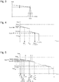
- the figure 3 illustrates examples of output voltage / output current control laws of a converter 30i for a given value of the input voltage of this converter.
- an output current regulation can be carried out at constant coefficient (solid line), at re-entering coefficient or at exiting coefficient, as illustrated.
- the auxiliary battery 5 is not connected to the network 6. It will be assumed that the input voltages at the terminals of the converters have the same order of magnitude, due in particular to the same number of stages d. 'electrochemical accumulators connected in series and of identical accumulator technology.
- the method of regulating the voltage on the network 6 proposed by the invention takes advantage of the tolerance of the voltage level of the network 6, and possibly of the auxiliary battery 5, the nominal voltages of which can vary by approximately 10.5 V 14V, corresponding respectively to the Vaux max values and min Vaux shown in figure 4 .
- the operation detailed in the diagram of the figure 4 corresponds to a simplified case with only two converters 301 and 302 exhibiting the same transformation law.
- the input voltage Ve1 of the converter 301 is greater than the input voltage Ve2 of the converter 302 (the state of charge of the accumulators of the stage connected to the input of the converter 301 is greater than the state of charge of the stage accumulators et2 connected to the input of converter 302). Consequently, the output voltage Vout1 of the converter 301 is greater than the output voltage Vout2 of the converter 302.
- the voltage Vomax1 corresponds to the no-load output voltage of the converter 301.
- the voltage Vomax2 corresponds to the no-load output voltage of the converter. converter 302.
- the current I aux called by network 6 is greater than the limit I1 max but less than the limit I1 max + I2 max .
- the output voltage Vout1 then drops below Vomax2 (current regulation of converter 301).
- the converter 302 thus supplies the complementary current I2 according to its transformation law (voltage regulation).
- the current is thus distributed over the different stages by discharging the most heavily loaded stages as a priority, which helps to balance the charges between the stages.
- balancing is carried out by supplying the network 6, the use of such balancing currents thus being optimized to limit unnecessary losses by dissipation.
- the greater the difference between the output voltages of the converters the more the auxiliary current is supplied primarily by the converter connected to a stage with the most load.
- such a balancing device 3 dispenses with complex interdependent regulation loops at the level of the converters, and moreover avoids having to resort to complex communication interfaces adapted to the voltage levels of the various stages.
- the converters 301 and 302 here have the same limax current limit. However, converters having different limits of limax intensity can of course be used within the framework of the invention.
- the operation detailed in the diagram of the figure 5 corresponds to a more complex case with a large number of converters 30i, or a case where the electrochemical accumulators of the different stages have a low voltage variation as a function of their state of charge. In such a case, an overlap between the output voltages of several converters 30i is probable.
- the converters 30i have the same transformation law.
- the converters are requested as a function of their no-load output voltage, as a function of their decrease slope (constant K2) and as a function of the auxiliary voltage values.
- converters 1 and 4 are connected to stages at the same state of charge and therefore have identical no-load voltages Vomax1 and Vomax4.
- the converters 301 and 304 each provide identical currents I1 and I4 (determined from the individual transformation law of each of these converters, not illustrated).
- converters 301, 303 and 304 supply currents distributed according to voltage Vaux, according to constant K2 and according to their respective off-load voltages.
- the point A is defined as the point for which the voltage Vaux is equal to the no-load voltage Vomax3.
- Point B is defined as the point for which the voltage Vaux is equal to Vomax1-K2 ⁇ I1max.
- the converters 301 and 304 each supply identical currents I1 max and I4 max .
- the converter 303 supplies the complementary current to reach a value iout3.
- Point C is defined as the point for which the voltage Vaux is equal to the voltage Vomax6.
- the voltage monitoring of the stages of the power battery 2 can advantageously be carried out by measuring the output voltages of the converters 30i.
- communication between a device for monitoring these voltage levels and a control circuit arranged at a low voltage level is facilitated.
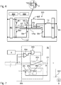
- the figure 6 illustrates an example of a converter 30i which is particularly advantageous for a balancing device according to the invention.
- the converter 30i has an FE input filter connected to the input connection interface.
- the output of the FE filter is connected to a full bridge inverter OP of a DC / DC converter circuit 303.
- the full bridge inverter includes controlled switches M1, M2, M3 and M4.
- the DC / DC converter circuit also includes a midpoint transformer at the secondary TPM.
- the TPM transformer has a primary winding EP connected as a bridge between switches M1 to M4.
- the switches M1 to M4 are controlled in pulse width modulation by a control circuit 320, in order to define the output voltage level.
- the 30i converter further includes a Synchronous rectifier including controlled switches M5 and M6.
- the secondary winding ES is connected between switches M5 and M6.
- the control circuit 320 can itself receive setpoint values from a regulation circuit 350, examples of which are detailed below.
- the TPM midpoint transformer minimizes the number of switches on the secondary to ensure signal rectification.
- the controlled switches M1 to M6 are controlled by the control circuit 320.
- the controlled switches M1 to M6 can have the structure shown: a transistor TM of the nMOS type with a free-rolling diode D connected in parallel. Such switches M5 and M6 are to be preferred instead of rectifying via diodes in order to maximize the efficiency of the conversion circuit 303.
- the use of MOSFET transistors also makes it possible to ensure bidirectional operation of the device. 30i converter.
- An output filter FS has its inputs connected between the midpoint of the secondary winding (via a storage inductor Ls) and a node common to switches M5 and M6.
- the outputs of the FS filter form the output interface of the converter 30i.
- a possible operating regime for a conversion circuit 303 can be a continuous conduction regime, operation applicable to any bidirectional converter in current, for example a converter as detailed with reference to the figure 6 .
- the conversion circuit 303 can be controlled at constant duty cycle, as long as the limax current limit is not reached.
- a switching frequency of 260KHz of the switches M1, M2, M3 and M4 can for example be used.
- the figure 7 illustrates an example of a converter 30i intended to implement a continuous conduction regime.
- the control circuit is here integrated into the DC / DC conversion circuit 303.
- the converter 30i includes a DC / DC conversion circuit 303 advantageously comprising galvanic isolation.
- the converter 30i further comprises a regulation circuit 350.
- the regulation circuit 350 generates a duty cycle ai the value of which is between 0 and 1.
- the regulation circuit 350 applies its duty cycle set point ai to the control circuit. control of the conversion circuit 303.
- the regulation circuit 350 does not use a closed voltage regulation loop here, limiting the output current proving sufficient.
- the regulation circuit 350 includes a subtractor 351 receiving the current li measured by the current sensor 31i on an inverting input, and the current limax on a non-inverting input.
- the subtracter 351 thus generates a current deviation signal ⁇ i to implement a closed current limiting loop.
- ⁇ i is applied to the input of a corrector 352, intended to develop a duty cycle value from this signal, by limiting the value of the duty cycle developed between a minimum value and a maximum value.
- This corrector 352 is for example of the PI (proportional integral) type.
- the output of the corrector 352 is applied to the input of a circuit 353.
- An areaf reference duty cycle value is also applied to another input of the circuit 353.
- the circuit 353 outputs the value ai, equal to the minimum between the two values applied to its input.
- ai is fixed at the value areaf.
- the value of areaf defines the open loop of output voltage regulation.
- the value ai is defined by the corrector 352 and therefore lowered, in order to reduce the output voltage of the conversion circuit 303.
- the control circuit 4 provides here only a binary activation or deactivation signal, applied to an input of an OR gate 355. Another input of the OR gate 355 is connected to the output of a comparator 354. The signal output of comparator 354 is applied to the conversion circuit 303 and thus allows to activate or deactivate the converter 30i.
- the comparator 354 makes it possible to deactivate the converter 30i if the voltage applied to its input by the stage Eti is less than the low threshold Veimin.
- f (li) 0, but it is also possible to provide a reduction in the duty cycle applied to the conversion circuit 303, as a function of the value li measured by the sensor 31i, in order to obtain a decrease in the voltage output with increasing li value.
- independently controlled converters 30i with the same output voltages distribute their contribution to the current i aux homogeneously.
- the figure 8 illustrates an example of a converter 30i intended to implement a discontinuous conduction regime.
- the control circuit is here integrated into the DC / DC conversion circuit 303.
- the converter 30i is here based on two nested closed regulation loops. A fast loop allows control of the output current li. A slow loop regulates the output voltage of the 30i converter.
- the converter 30 i comprises a regulation circuit 350.
- the regulation circuit 350 generates a duty cycle ai the value of which is between 0 and 1.
- the regulation circuit 350 applies its duty cycle set point ai to the control circuit of the circuit. conversion 303.
- the regulation circuit 350 comprises a subtracter 351 receiving the current li measured by the current sensor 31i on an inverting input, and a current Iref (detailed below) on a non-inverting input.
- the subtracter 351 thus generates a current deviation signal ⁇ i.
- ⁇ i is applied to the input of a corrector 352, intended to develop a duty cycle value from this signal, by limiting the value of the duty cycle developed between a minimum value and a maximum value.
- This corrector 352 is for example of the PI (proportional integral) type.
- the output of the corrector 352 applies the duty cycle ⁇ 1 to a control input of the conversion circuit 303.
- the voltage value Vi is applied to a non-inverting input of a subtracter 357.
- a voltage sensor 36i measures the output voltage of the conversion circuit 303 and applies this voltage value to the inverting input of the subtracter 357.
- a signal voltage error ⁇ v is thus generated.
- the signal ⁇ v is applied to the input of a corrector 358 (for example of type PI).
- the corrector 358 generates the current reference iref.
- the slow loop is active as long as the current setpoint iref is lower than the limax value.
- the output current of the conversion circuit 303 is limited to limax.
- control circuit 4 provides here only a binary activation or deactivation signal, applied to an input of an OR gate 355.
- Another input of the OR gate 355 is connected to the output of a comparator 354.
- the output signal of comparator 354 is applied to conversion circuit 303.
- the figures 9 and 10 illustrate examples of one-way converters further having a switch function in series with the DC / DC conversion circuit.
- the switch function allows the converter to be isolated in the event of a fault.
- the unidirectional conduction function is intended to prevent the converter, having an output voltage lower than that of the auxiliary network or of another converter to which it is connected, from being passed through by a current to the stage connected to its input.
- these functions are performed by a circuit connected in series between the output of a converter and the output of its conversion circuit.
- the converters 30k and 30 (k-1) thus comprise respective circuits 34k and 34 (k-1).
- Each of these circuits 34k and 34 (k-1) comprises a MOSFET transistor controlled by a control circuit not shown. This variant makes it possible to limit the losses for implementing these switch and monodirectional conduction functions.
- the use of a MOFSET transistor also allows bidirectional current operation.
- the invention is advantageously applied with electrical energy storage devices 2 including electrochemical accumulators whose voltage variation at their terminals is significant during a variation in their residual charge.
- the charging and discharging of an electrochemical accumulator results in an increase or decrease in the voltage at its terminals, respectively.
- the nominal voltage at the terminals of an electrochemical accumulator is fixed by the electrochemical characteristics of the materials used.
- the operating voltage of an accumulator depends on its nominal voltage but also on the current flowing through it, its internal resistance, its temperature, its aging and its residual charge.
- the curves shown in figure 11 illustrate typical discharges for different technologies of electrochemical accumulators discharged at a discharge current of 0.2 C.
- a Li-ion battery based on iron phosphate presents a typical voltage level which varies little as a function of the discharge current: a variation of the order of 5.5% is typically observed with respect to the nominal voltage between 10% and 90% of the residual charge of the accumulator.
- a lead acid (Pb) -based accumulator exhibits a typical variation in the voltage at its terminals more pronounced (approximately 10%) for this same variation in charge.
- An alkaline accumulator based on zinc and manganese dioxide (Zn / MnO2) exhibits an even more pronounced variation in the voltage at its terminals (approximately 44%) for this same variation in charge.
- a Li-ion accumulator with a positive electrode containing cobalt (NMC, NCA, LiCoO2, etc.) has a typical voltage variation across its terminals of around 12% for this same variation in charge.
- one or more stages of the battery are recharged.
- Such recharging of one or more stages can be ensured by discharging one or more other stages exhibiting a higher state of charge, via their respective converters (for example a converter as detailed with reference to figure 6 ).
- the converters 30i will then advantageously also have an Irimax recharge limit.
- the figure 12 illustrates an example of an output voltage / current output diagram of such a converter 30i. It is preferable to limit the recharging resistance of 30i converters to avoid losses during balancing between stages.
- the electric power supply system 1 advantageously comprises a device for measuring and monitoring the voltage at the terminals of the accumulator stages Et i .
Landscapes
- Engineering & Computer Science (AREA)
- Power Engineering (AREA)
- Dc-Dc Converters (AREA)
- Charge And Discharge Circuits For Batteries Or The Like (AREA)
- Direct Current Feeding And Distribution (AREA)
- Secondary Cells (AREA)
Claims (13)
- Vorrichtung zum Ausgleich (3) der Ladung einer elektrischen Leistungsspeichervorrichtung (2) mit mehreren in Reihe geschalteten elektrischen Speicherelementen (Et1, ... Etk), dadurch gekennzeichnet, dass sie Folgendes aufweist:- mindestens zwei DC/DC-Wandler (30i) mit Strombegrenzung, von denen jeder Folgendes aufweist:- einen Eingang, der dazu bestimmt ist, an die Klemmen eines jeweiligen Speicherelements (Eti) angeschlossen zu werden;- einen Ausgang, der dazu bestimmt ist, an ein elektrisches Netz (6) angeschlossen zu werden, dessen Spannung auf einen Pegel geregelt ist, der niedriger ist als die Spannung an den Anschlüssen der Speichervorrichtung (2);- ein Transformationsgesetz vom Typ Vout=K1∗Ve-f(I) für I≤Iimax, wobei Vout die Potentialdifferenz an dem Ausgang ist, K1 eine Konstante ist, Ve die Potentialdifferenz an dem Eingang ist, f(l) eine affine Funktion des Stroms I ist, der an dem Ausgang abgegeben wird, und limax die Strombegrenzung des Wandlers ist und f(Iimax)<K1∗Ve ist;- einen Stromregelungsbetrieb, wenn I den Wert limax erreicht.
- Vorrichtung (3) zum Ausgleich der Ladung einer elektrischen Leistungsspeichervorrichtung nach Anspruch 1, wobei jeder der Wandler eine Schaltung zum Messen des Stroms aufweist, der an seinem Ausgang abgegeben wird.
- Vorrichtung (3) zum Ausgleich der Ladung einer elektrischen Leistungsspeichervorrichtung nach Anspruch 2, wobei jeder der Wandler eine Schaltung zum Regeln aufweist, die das Transformationsgesetz in Abhängigkeit vom gemessenen Strom anwendet.
- Vorrichtung (3) zum Ausgleich der Ladung einer elektrischen Leistungsspeichervorrichtung nach Anspruch 2 oder 3, wobei jeder der Wandler eine Induktivität (Ls) aufweist, die an seinem Ausgang angeschlossen ist, und eine Schaltung zum Regeln aufweist, die den Wandler im Dauerbetrieb hält, solange der am Ausgang abgegebene Strom unter dem Wert limax liegt.
- Vorrichtung zum Ausgleich der Ladung einer elektrischen Leistungsspeichervorrichtung nach einem der vorhergehenden Ansprüche, wobei K1 eine Konstante ist, deren Wert zwischen 0 und 1 liegt.
- Vorrichtung zum Ausgleich der Ladung einer elektrischen Leistungsspeichervorrichtung nach einem der vorhergehenden Ansprüche, wobei f(l) < 0,1∗K1∗Ve.
- Vorrichtung zum Ausgleich der Ladung einer elektrischen Leistungsspeichervorrichtung nach einem der vorhergehenden Ansprüche, wobei die Wandler vom Typ bidirektionaler Stromwandler sind.
- Vorrichtung zum Ausgleich der Ladung einer elektrischen Leistungsspeichervorrichtung nach Anspruch 7, wobei die Wandler jeweils einen Transformator (TPM) enthalten, von dem eine Primärwicklung (EP) in einer Brücke zwischen vier über Pulsweitenmodulation gesteuerte Schalter angeschlossen ist.
- Vorrichtung zum Ausgleich der Ladung nach Anspruch 8, wobei der Transformator (TPM) ein Transformator mit Mittelanzapfung ist, von dem eine Sekundärwicklung (ES) zwischen zwei gesteuerten Schaltern angeschlossen ist, wobei die Sekundärwicklung (ES) eine Mittelanzapfung aufweist, die an einen Ausgang des zugehörigen Wandlers angeschlossen ist.
- Vorrichtung (3) zum Ausgleich der Ladung einer elektrischen Leistungsspeichervorrichtung nach einem der vorhergehenden Ansprüche, wobei f(I) eine streng positive affine Funktion ist, wenn der Ausgang des entsprechenden Wandlers Strom abgibt.
- Vorrichtung zum Ausgleich der Ladung nach einem der vorhergehenden Ansprüche, wobei die Werte K1, limax und die Funktion f(l) für jeden der DC/DC-Wandler identisch sind.
- Stromversorgungssystem (1), das Folgendes aufweist:- eine Vorrichtung (3) zum Ausgleich der Ladung nach einem der vorhergehenden Ansprüche;- eine elektrische Leistungsspeichervorrichtung (2) mit mehreren elektrischen Speicherelementen, wobei diese Elemente an die jeweiligen Wandler der Vorrichtung zum Ausgleich der Ladung (3) angeschlossen sind;- ein elektrisches Netz (6), das an die Vorrichtung zum Ausgleich der Ladung angeschlossen ist und dessen Spannung auf einen Pegel geregelt ist, der niedriger ist als die Spannung an den Anschlüssen der Speichervorrichtung (2).
- System nach Anspruch 12, wobei die elektrischen Speicherelemente elektrochemische Akkumulatoren sind, bei denen die Spannungsänderung zwischen 90 und 10 % ihres Ladezustands mindestens 10 % ihrer Nennspannung beträgt.
Applications Claiming Priority (2)
| Application Number | Priority Date | Filing Date | Title |
|---|---|---|---|
| FR1358062A FR3009903B1 (fr) | 2013-08-20 | 2013-08-20 | Dispositif d'equilibrage de charge des elements d'un batterie de puissance |
| PCT/EP2014/065976 WO2015024731A2 (fr) | 2013-08-20 | 2014-07-24 | Dispositif d'equilibrage de charge des elements d'une batterie de puissance |
Publications (2)
| Publication Number | Publication Date |
|---|---|
| EP3036818A2 EP3036818A2 (de) | 2016-06-29 |
| EP3036818B1 true EP3036818B1 (de) | 2020-08-05 |
Family
ID=50069012
Family Applications (1)
| Application Number | Title | Priority Date | Filing Date |
|---|---|---|---|
| EP14742250.5A Not-in-force EP3036818B1 (de) | 2013-08-20 | 2014-07-24 | Vorrichtung zum ausgleich der ladung von elementen einer strombatterie |
Country Status (5)
| Country | Link |
|---|---|
| US (1) | US9997931B2 (de) |
| EP (1) | EP3036818B1 (de) |
| JP (1) | JP6427574B2 (de) |
| FR (1) | FR3009903B1 (de) |
| WO (1) | WO2015024731A2 (de) |
Families Citing this family (11)
| Publication number | Priority date | Publication date | Assignee | Title |
|---|---|---|---|---|
| DE102017206254B4 (de) * | 2016-04-13 | 2024-07-11 | Dialog Semiconductor (Uk) Limited | DC-DC-Umwandlung für Mehrzellen-Batterien |
| US9912177B2 (en) * | 2016-06-17 | 2018-03-06 | Qualcomm Incorporated | Single transformer high-power balancer |
| JP6928347B2 (ja) * | 2017-08-02 | 2021-09-01 | NExT−e Solutions株式会社 | 管理装置、蓄電装置、蓄電システム、及び、電気機器 |
| CN107294177B (zh) * | 2017-08-07 | 2023-07-04 | 上海山源电子科技股份有限公司 | 一种本安矿灯充电系统及其充电方法 |
| US10879519B2 (en) | 2018-12-17 | 2020-12-29 | Bayco Products, Inc. | Spark protection apparatus for intrinsically safe, battery-operated devices |
| FR3101488B1 (fr) * | 2019-10-01 | 2021-09-03 | Commissariat Energie Atomique | Unité de conversion électrique pour module de stockage d’énergie électrique |
| US11569668B2 (en) * | 2020-07-14 | 2023-01-31 | Igrenenergi, Inc. | System and method for dynamic balancing power in a battery pack |
| CN113708466B (zh) * | 2021-10-25 | 2022-03-11 | 广东希荻微电子股份有限公司 | 一种电池充放电电路和终端设备 |
| EP4173872A1 (de) * | 2021-11-02 | 2023-05-03 | Vitesco Technologies GmbH | Verfahren zur steuerung eines batteriesystems |
| FR3130457A1 (fr) * | 2021-12-13 | 2023-06-16 | Powzl | Generateur electrique comportant une pluralite de batteries |
| JP2026031021A (ja) * | 2024-08-09 | 2026-02-24 | トヨタ自動車株式会社 | 蓄電池システム |
Family Cites Families (8)
| Publication number | Priority date | Publication date | Assignee | Title |
|---|---|---|---|---|
| US4717833A (en) | 1984-04-30 | 1988-01-05 | Boschert Inc. | Single wire current share paralleling of power supplies |
| JPH07337001A (ja) * | 1994-06-07 | 1995-12-22 | Hitachi Ltd | 電源装置 |
| US7378818B2 (en) * | 2002-11-25 | 2008-05-27 | Tiax Llc | Bidirectional power converter for balancing state of charge among series connected electrical energy storage units |
| US6873134B2 (en) * | 2003-07-21 | 2005-03-29 | The Boeing Company | Autonomous battery cell balancing system with integrated voltage monitoring |
| US7592775B2 (en) * | 2006-05-31 | 2009-09-22 | Aeroflex Plainview, Inc. | Battery balancing including resonant frequency compensation |
| CN101521083A (zh) | 2008-11-25 | 2009-09-02 | 天水电气传动研究所有限责任公司 | 用igbt实现的超导磁铁电源 |
| FR2959885B1 (fr) * | 2010-05-05 | 2014-12-05 | Commissariat Energie Atomique | Systeme d'equilibrage pour batterie de puissance, procede d'equilibrage de charge et procede combine d'equilibrage de charge et d'alimentation correspondants |
| FR2982090B1 (fr) * | 2011-10-31 | 2013-12-20 | Commissariat Energie Atomique | Dispositif d'equilibrage de charge des elements d'une batterie de puissance |
-
2013
- 2013-08-20 FR FR1358062A patent/FR3009903B1/fr not_active Expired - Fee Related
-
2014
- 2014-07-24 JP JP2016535385A patent/JP6427574B2/ja not_active Expired - Fee Related
- 2014-07-24 WO PCT/EP2014/065976 patent/WO2015024731A2/fr not_active Ceased
- 2014-07-24 US US14/911,221 patent/US9997931B2/en active Active
- 2014-07-24 EP EP14742250.5A patent/EP3036818B1/de not_active Not-in-force
Non-Patent Citations (1)
| Title |
|---|
| None * |
Also Published As
| Publication number | Publication date |
|---|---|
| JP6427574B2 (ja) | 2018-11-21 |
| US9997931B2 (en) | 2018-06-12 |
| FR3009903A1 (fr) | 2015-02-27 |
| JP2016528868A (ja) | 2016-09-15 |
| FR3009903B1 (fr) | 2016-12-30 |
| US20160197498A1 (en) | 2016-07-07 |
| EP3036818A2 (de) | 2016-06-29 |
| WO2015024731A2 (fr) | 2015-02-26 |
| WO2015024731A3 (fr) | 2015-06-18 |
Similar Documents
| Publication | Publication Date | Title |
|---|---|---|
| EP3036818B1 (de) | Vorrichtung zum ausgleich der ladung von elementen einer strombatterie | |
| EP2774240B1 (de) | Vorrichtung zum ausgleich der ladung von elementen einer strombatterie | |
| EP2532069B1 (de) | Ladungsausgleichssystem für batterien | |
| EP2684274B1 (de) | Ladungsausgleichssysteme für batterien | |
| EP3075058B1 (de) | Vorrichtung zum auswuchten der last eines hochleistungsbatterieelements | |
| EP2532068B1 (de) | Ladungsausgleich für batterien | |
| US10081259B2 (en) | Charging facility and energy management method for charging facility | |
| EP2532070B1 (de) | Ausgleichssystem für akkumulatoren | |
| EP2781001B1 (de) | Gleichspannungsquelle einschliesslich brennstoffzellen mit anpassungfähigem spannungspegel | |
| EP2567443A2 (de) | Ausgleichssystem für strombatterie und entsprechende lastverteilungsmethode | |
| CN102195333A (zh) | 直流电源装置 | |
| FR3064848A1 (fr) | Procede de commande d'un dispositif de charge embarque sur un vehicule electrique ou hybride. | |
| US20180233929A1 (en) | Battery to battery charger using asymmetric batteries | |
| JP6214607B2 (ja) | 蓄電装置及び輸送機器 | |
| JP2009296719A (ja) | 直流バックアップ電源システムおよびその充電方法 | |
| FR2994896A1 (fr) | Dispositif de stockage d'electricite comportant une batterie a haute tension et une batterie a basse tension de type lithium-ion | |
| JP5275889B2 (ja) | 充電装置および充電方法 | |
| WO2022018226A1 (fr) | Systeme d'alimentation d'un moteur de traction | |
| FR3159118A1 (fr) | Procédé de contrôle de puissance d’un réseau haute tension de véhicule électrifié |
Legal Events
| Date | Code | Title | Description |
|---|---|---|---|
| PUAI | Public reference made under article 153(3) epc to a published international application that has entered the european phase |
Free format text: ORIGINAL CODE: 0009012 |
|
| 17P | Request for examination filed |
Effective date: 20160210 |
|
| AK | Designated contracting states |
Kind code of ref document: A2 Designated state(s): AL AT BE BG CH CY CZ DE DK EE ES FI FR GB GR HR HU IE IS IT LI LT LU LV MC MK MT NL NO PL PT RO RS SE SI SK SM TR |
|
| AX | Request for extension of the european patent |
Extension state: BA ME |
|
| DAX | Request for extension of the european patent (deleted) | ||
| GRAP | Despatch of communication of intention to grant a patent |
Free format text: ORIGINAL CODE: EPIDOSNIGR1 |
|
| STAA | Information on the status of an ep patent application or granted ep patent |
Free format text: STATUS: GRANT OF PATENT IS INTENDED |
|
| INTG | Intention to grant announced |
Effective date: 20200221 |
|
| GRAS | Grant fee paid |
Free format text: ORIGINAL CODE: EPIDOSNIGR3 |
|
| GRAA | (expected) grant |
Free format text: ORIGINAL CODE: 0009210 |
|
| STAA | Information on the status of an ep patent application or granted ep patent |
Free format text: STATUS: THE PATENT HAS BEEN GRANTED |
|
| AK | Designated contracting states |
Kind code of ref document: B1 Designated state(s): AL AT BE BG CH CY CZ DE DK EE ES FI FR GB GR HR HU IE IS IT LI LT LU LV MC MK MT NL NO PL PT RO RS SE SI SK SM TR |
|
| REG | Reference to a national code |
Ref country code: GB Ref legal event code: FG4D Free format text: NOT ENGLISH |
|
| REG | Reference to a national code |
Ref country code: CH Ref legal event code: EP |
|
| REG | Reference to a national code |
Ref country code: AT Ref legal event code: REF Ref document number: 1300077 Country of ref document: AT Kind code of ref document: T Effective date: 20200815 |
|
| REG | Reference to a national code |
Ref country code: DE Ref legal event code: R096 Ref document number: 602014068583 Country of ref document: DE |
|
| REG | Reference to a national code |
Ref country code: IE Ref legal event code: FG4D Free format text: LANGUAGE OF EP DOCUMENT: FRENCH |
|
| REG | Reference to a national code |
Ref country code: LT Ref legal event code: MG4D |
|
| REG | Reference to a national code |
Ref country code: NL Ref legal event code: MP Effective date: 20200805 |
|
| REG | Reference to a national code |
Ref country code: AT Ref legal event code: MK05 Ref document number: 1300077 Country of ref document: AT Kind code of ref document: T Effective date: 20200805 |
|
| PG25 | Lapsed in a contracting state [announced via postgrant information from national office to epo] |
Ref country code: PT Free format text: LAPSE BECAUSE OF FAILURE TO SUBMIT A TRANSLATION OF THE DESCRIPTION OR TO PAY THE FEE WITHIN THE PRESCRIBED TIME-LIMIT Effective date: 20201207 Ref country code: HR Free format text: LAPSE BECAUSE OF FAILURE TO SUBMIT A TRANSLATION OF THE DESCRIPTION OR TO PAY THE FEE WITHIN THE PRESCRIBED TIME-LIMIT Effective date: 20200805 Ref country code: LT Free format text: LAPSE BECAUSE OF FAILURE TO SUBMIT A TRANSLATION OF THE DESCRIPTION OR TO PAY THE FEE WITHIN THE PRESCRIBED TIME-LIMIT Effective date: 20200805 Ref country code: FI Free format text: LAPSE BECAUSE OF FAILURE TO SUBMIT A TRANSLATION OF THE DESCRIPTION OR TO PAY THE FEE WITHIN THE PRESCRIBED TIME-LIMIT Effective date: 20200805 Ref country code: AT Free format text: LAPSE BECAUSE OF FAILURE TO SUBMIT A TRANSLATION OF THE DESCRIPTION OR TO PAY THE FEE WITHIN THE PRESCRIBED TIME-LIMIT Effective date: 20200805 Ref country code: NO Free format text: LAPSE BECAUSE OF FAILURE TO SUBMIT A TRANSLATION OF THE DESCRIPTION OR TO PAY THE FEE WITHIN THE PRESCRIBED TIME-LIMIT Effective date: 20201105 Ref country code: ES Free format text: LAPSE BECAUSE OF FAILURE TO SUBMIT A TRANSLATION OF THE DESCRIPTION OR TO PAY THE FEE WITHIN THE PRESCRIBED TIME-LIMIT Effective date: 20200805 Ref country code: GR Free format text: LAPSE BECAUSE OF FAILURE TO SUBMIT A TRANSLATION OF THE DESCRIPTION OR TO PAY THE FEE WITHIN THE PRESCRIBED TIME-LIMIT Effective date: 20201106 Ref country code: BG Free format text: LAPSE BECAUSE OF FAILURE TO SUBMIT A TRANSLATION OF THE DESCRIPTION OR TO PAY THE FEE WITHIN THE PRESCRIBED TIME-LIMIT Effective date: 20201105 Ref country code: SE Free format text: LAPSE BECAUSE OF FAILURE TO SUBMIT A TRANSLATION OF THE DESCRIPTION OR TO PAY THE FEE WITHIN THE PRESCRIBED TIME-LIMIT Effective date: 20200805 |
|
| PG25 | Lapsed in a contracting state [announced via postgrant information from national office to epo] |
Ref country code: IS Free format text: LAPSE BECAUSE OF FAILURE TO SUBMIT A TRANSLATION OF THE DESCRIPTION OR TO PAY THE FEE WITHIN THE PRESCRIBED TIME-LIMIT Effective date: 20201205 Ref country code: NL Free format text: LAPSE BECAUSE OF FAILURE TO SUBMIT A TRANSLATION OF THE DESCRIPTION OR TO PAY THE FEE WITHIN THE PRESCRIBED TIME-LIMIT Effective date: 20200805 Ref country code: LV Free format text: LAPSE BECAUSE OF FAILURE TO SUBMIT A TRANSLATION OF THE DESCRIPTION OR TO PAY THE FEE WITHIN THE PRESCRIBED TIME-LIMIT Effective date: 20200805 Ref country code: PL Free format text: LAPSE BECAUSE OF FAILURE TO SUBMIT A TRANSLATION OF THE DESCRIPTION OR TO PAY THE FEE WITHIN THE PRESCRIBED TIME-LIMIT Effective date: 20200805 Ref country code: RS Free format text: LAPSE BECAUSE OF FAILURE TO SUBMIT A TRANSLATION OF THE DESCRIPTION OR TO PAY THE FEE WITHIN THE PRESCRIBED TIME-LIMIT Effective date: 20200805 |
|
| PG25 | Lapsed in a contracting state [announced via postgrant information from national office to epo] |
Ref country code: EE Free format text: LAPSE BECAUSE OF FAILURE TO SUBMIT A TRANSLATION OF THE DESCRIPTION OR TO PAY THE FEE WITHIN THE PRESCRIBED TIME-LIMIT Effective date: 20200805 Ref country code: DK Free format text: LAPSE BECAUSE OF FAILURE TO SUBMIT A TRANSLATION OF THE DESCRIPTION OR TO PAY THE FEE WITHIN THE PRESCRIBED TIME-LIMIT Effective date: 20200805 Ref country code: CZ Free format text: LAPSE BECAUSE OF FAILURE TO SUBMIT A TRANSLATION OF THE DESCRIPTION OR TO PAY THE FEE WITHIN THE PRESCRIBED TIME-LIMIT Effective date: 20200805 Ref country code: RO Free format text: LAPSE BECAUSE OF FAILURE TO SUBMIT A TRANSLATION OF THE DESCRIPTION OR TO PAY THE FEE WITHIN THE PRESCRIBED TIME-LIMIT Effective date: 20200805 Ref country code: SM Free format text: LAPSE BECAUSE OF FAILURE TO SUBMIT A TRANSLATION OF THE DESCRIPTION OR TO PAY THE FEE WITHIN THE PRESCRIBED TIME-LIMIT Effective date: 20200805 |
|
| REG | Reference to a national code |
Ref country code: DE Ref legal event code: R097 Ref document number: 602014068583 Country of ref document: DE |
|
| PG25 | Lapsed in a contracting state [announced via postgrant information from national office to epo] |
Ref country code: AL Free format text: LAPSE BECAUSE OF FAILURE TO SUBMIT A TRANSLATION OF THE DESCRIPTION OR TO PAY THE FEE WITHIN THE PRESCRIBED TIME-LIMIT Effective date: 20200805 |
|
| PLBE | No opposition filed within time limit |
Free format text: ORIGINAL CODE: 0009261 |
|
| STAA | Information on the status of an ep patent application or granted ep patent |
Free format text: STATUS: NO OPPOSITION FILED WITHIN TIME LIMIT |
|
| PG25 | Lapsed in a contracting state [announced via postgrant information from national office to epo] |
Ref country code: SK Free format text: LAPSE BECAUSE OF FAILURE TO SUBMIT A TRANSLATION OF THE DESCRIPTION OR TO PAY THE FEE WITHIN THE PRESCRIBED TIME-LIMIT Effective date: 20200805 |
|
| 26N | No opposition filed |
Effective date: 20210507 |
|
| PG25 | Lapsed in a contracting state [announced via postgrant information from national office to epo] |
Ref country code: IT Free format text: LAPSE BECAUSE OF FAILURE TO SUBMIT A TRANSLATION OF THE DESCRIPTION OR TO PAY THE FEE WITHIN THE PRESCRIBED TIME-LIMIT Effective date: 20200805 |
|
| PG25 | Lapsed in a contracting state [announced via postgrant information from national office to epo] |
Ref country code: SI Free format text: LAPSE BECAUSE OF FAILURE TO SUBMIT A TRANSLATION OF THE DESCRIPTION OR TO PAY THE FEE WITHIN THE PRESCRIBED TIME-LIMIT Effective date: 20200805 |
|
| REG | Reference to a national code |
Ref country code: CH Ref legal event code: PL |
|
| GBPC | Gb: european patent ceased through non-payment of renewal fee |
Effective date: 20210724 |
|
| PG25 | Lapsed in a contracting state [announced via postgrant information from national office to epo] |
Ref country code: MC Free format text: LAPSE BECAUSE OF FAILURE TO SUBMIT A TRANSLATION OF THE DESCRIPTION OR TO PAY THE FEE WITHIN THE PRESCRIBED TIME-LIMIT Effective date: 20200805 |
|
| REG | Reference to a national code |
Ref country code: BE Ref legal event code: MM Effective date: 20210731 |
|
| PG25 | Lapsed in a contracting state [announced via postgrant information from national office to epo] |
Ref country code: LI Free format text: LAPSE BECAUSE OF NON-PAYMENT OF DUE FEES Effective date: 20210731 Ref country code: GB Free format text: LAPSE BECAUSE OF NON-PAYMENT OF DUE FEES Effective date: 20210724 Ref country code: CH Free format text: LAPSE BECAUSE OF NON-PAYMENT OF DUE FEES Effective date: 20210731 |
|
| PG25 | Lapsed in a contracting state [announced via postgrant information from national office to epo] |
Ref country code: LU Free format text: LAPSE BECAUSE OF NON-PAYMENT OF DUE FEES Effective date: 20210724 |
|
| PG25 | Lapsed in a contracting state [announced via postgrant information from national office to epo] |
Ref country code: IE Free format text: LAPSE BECAUSE OF NON-PAYMENT OF DUE FEES Effective date: 20210724 Ref country code: BE Free format text: LAPSE BECAUSE OF NON-PAYMENT OF DUE FEES Effective date: 20210731 |
|
| PG25 | Lapsed in a contracting state [announced via postgrant information from national office to epo] |
Ref country code: HU Free format text: LAPSE BECAUSE OF FAILURE TO SUBMIT A TRANSLATION OF THE DESCRIPTION OR TO PAY THE FEE WITHIN THE PRESCRIBED TIME-LIMIT; INVALID AB INITIO Effective date: 20140724 |
|
| PG25 | Lapsed in a contracting state [announced via postgrant information from national office to epo] |
Ref country code: CY Free format text: LAPSE BECAUSE OF FAILURE TO SUBMIT A TRANSLATION OF THE DESCRIPTION OR TO PAY THE FEE WITHIN THE PRESCRIBED TIME-LIMIT Effective date: 20200805 |
|
| PG25 | Lapsed in a contracting state [announced via postgrant information from national office to epo] |
Ref country code: MK Free format text: LAPSE BECAUSE OF FAILURE TO SUBMIT A TRANSLATION OF THE DESCRIPTION OR TO PAY THE FEE WITHIN THE PRESCRIBED TIME-LIMIT Effective date: 20200805 |
|
| PG25 | Lapsed in a contracting state [announced via postgrant information from national office to epo] |
Ref country code: MT Free format text: LAPSE BECAUSE OF FAILURE TO SUBMIT A TRANSLATION OF THE DESCRIPTION OR TO PAY THE FEE WITHIN THE PRESCRIBED TIME-LIMIT Effective date: 20200805 |
|
| PGFP | Annual fee paid to national office [announced via postgrant information from national office to epo] |
Ref country code: DE Payment date: 20240719 Year of fee payment: 11 |
|
| PGFP | Annual fee paid to national office [announced via postgrant information from national office to epo] |
Ref country code: FR Payment date: 20240723 Year of fee payment: 11 |
|
| PG25 | Lapsed in a contracting state [announced via postgrant information from national office to epo] |
Ref country code: TR Free format text: LAPSE BECAUSE OF FAILURE TO SUBMIT A TRANSLATION OF THE DESCRIPTION OR TO PAY THE FEE WITHIN THE PRESCRIBED TIME-LIMIT Effective date: 20200805 |
|
| REG | Reference to a national code |
Ref country code: DE Ref legal event code: R119 Ref document number: 602014068583 Country of ref document: DE |
|
| PG25 | Lapsed in a contracting state [announced via postgrant information from national office to epo] |
Ref country code: DE Free format text: LAPSE BECAUSE OF NON-PAYMENT OF DUE FEES Effective date: 20260203 |
|
| PG25 | Lapsed in a contracting state [announced via postgrant information from national office to epo] |
Ref country code: FR Free format text: LAPSE BECAUSE OF NON-PAYMENT OF DUE FEES Effective date: 20250731 |