EP3038436B1 - Fabrication d'un systeme de commutation comprenant des trous metallises - Google Patents
Fabrication d'un systeme de commutation comprenant des trous metallises Download PDFInfo
- Publication number
- EP3038436B1 EP3038436B1 EP15197167.8A EP15197167A EP3038436B1 EP 3038436 B1 EP3038436 B1 EP 3038436B1 EP 15197167 A EP15197167 A EP 15197167A EP 3038436 B1 EP3038436 B1 EP 3038436B1
- Authority
- EP
- European Patent Office
- Prior art keywords
- vias
- circuit board
- thermal
- thermal vias
- solder
- Prior art date
- Legal status (The legal status is an assumption and is not a legal conclusion. Google has not performed a legal analysis and makes no representation as to the accuracy of the status listed.)
- Active
Links
Images


Classifications
-
- H—ELECTRICITY
- H05—ELECTRIC TECHNIQUES NOT OTHERWISE PROVIDED FOR
- H05K—PRINTED CIRCUITS; CASINGS OR CONSTRUCTIONAL DETAILS OF ELECTRIC APPARATUS; MANUFACTURE OF ASSEMBLAGES OF ELECTRICAL COMPONENTS
- H05K1/00—Printed circuits
- H05K1/02—Details
- H05K1/0201—Thermal arrangements, e.g. for cooling, heating or preventing overheating
- H05K1/0203—Cooling of mounted components
- H05K1/0204—Cooling of mounted components using means for thermal conduction connection in the thickness direction of the substrate
- H05K1/0206—Cooling of mounted components using means for thermal conduction connection in the thickness direction of the substrate by printed thermal vias
-
- H—ELECTRICITY
- H05—ELECTRIC TECHNIQUES NOT OTHERWISE PROVIDED FOR
- H05K—PRINTED CIRCUITS; CASINGS OR CONSTRUCTIONAL DETAILS OF ELECTRIC APPARATUS; MANUFACTURE OF ASSEMBLAGES OF ELECTRICAL COMPONENTS
- H05K3/00—Apparatus or processes for manufacturing printed circuits
- H05K3/0094—Filling or covering plated through-holes or blind plated vias, e.g. for masking or for mechanical reinforcement
-
- H—ELECTRICITY
- H05—ELECTRIC TECHNIQUES NOT OTHERWISE PROVIDED FOR
- H05K—PRINTED CIRCUITS; CASINGS OR CONSTRUCTIONAL DETAILS OF ELECTRIC APPARATUS; MANUFACTURE OF ASSEMBLAGES OF ELECTRICAL COMPONENTS
- H05K3/00—Apparatus or processes for manufacturing printed circuits
- H05K3/30—Assembling printed circuits with electric components, e.g. with resistors
- H05K3/32—Assembling printed circuits with electric components, e.g. with resistors electrically connecting electric components or wires to printed circuits
- H05K3/34—Assembling printed circuits with electric components, e.g. with resistors electrically connecting electric components or wires to printed circuits by soldering
-
- H—ELECTRICITY
- H05—ELECTRIC TECHNIQUES NOT OTHERWISE PROVIDED FOR
- H05K—PRINTED CIRCUITS; CASINGS OR CONSTRUCTIONAL DETAILS OF ELECTRIC APPARATUS; MANUFACTURE OF ASSEMBLAGES OF ELECTRICAL COMPONENTS
- H05K3/00—Apparatus or processes for manufacturing printed circuits
- H05K3/30—Assembling printed circuits with electric components, e.g. with resistors
- H05K3/32—Assembling printed circuits with electric components, e.g. with resistors electrically connecting electric components or wires to printed circuits
- H05K3/34—Assembling printed circuits with electric components, e.g. with resistors electrically connecting electric components or wires to printed circuits by soldering
- H05K3/341—Surface mounted components
-
- H—ELECTRICITY
- H05—ELECTRIC TECHNIQUES NOT OTHERWISE PROVIDED FOR
- H05K—PRINTED CIRCUITS; CASINGS OR CONSTRUCTIONAL DETAILS OF ELECTRIC APPARATUS; MANUFACTURE OF ASSEMBLAGES OF ELECTRICAL COMPONENTS
- H05K7/00—Constructional details common to different types of electric apparatus
- H05K7/20—Modifications to facilitate cooling, ventilating, or heating
- H05K7/2039—Modifications to facilitate cooling, ventilating, or heating characterised by the heat transfer by conduction from the heat generating element to a dissipating body
- H05K7/205—Heat-dissipating body thermally connected to heat generating element via thermal paths through printed circuit board [PCB]
-
- H—ELECTRICITY
- H05—ELECTRIC TECHNIQUES NOT OTHERWISE PROVIDED FOR
- H05K—PRINTED CIRCUITS; CASINGS OR CONSTRUCTIONAL DETAILS OF ELECTRIC APPARATUS; MANUFACTURE OF ASSEMBLAGES OF ELECTRICAL COMPONENTS
- H05K7/00—Constructional details common to different types of electric apparatus
- H05K7/20—Modifications to facilitate cooling, ventilating, or heating
- H05K7/20845—Modifications to facilitate cooling, ventilating, or heating for automotive electronic casings
- H05K7/20854—Heat transfer by conduction from internal heat source to heat radiating structure
-
- H—ELECTRICITY
- H05—ELECTRIC TECHNIQUES NOT OTHERWISE PROVIDED FOR
- H05K—PRINTED CIRCUITS; CASINGS OR CONSTRUCTIONAL DETAILS OF ELECTRIC APPARATUS; MANUFACTURE OF ASSEMBLAGES OF ELECTRICAL COMPONENTS
- H05K1/00—Printed circuits
- H05K1/02—Details
- H05K1/11—Printed elements for providing electric connections to or between printed circuits
- H05K1/111—Pads for surface mounting, e.g. lay-out
- H05K1/112—Pads for surface mounting, e.g. lay-out directly combined with via connections
- H05K1/113—Via provided in pad; Pad over filled via
-
- H—ELECTRICITY
- H05—ELECTRIC TECHNIQUES NOT OTHERWISE PROVIDED FOR
- H05K—PRINTED CIRCUITS; CASINGS OR CONSTRUCTIONAL DETAILS OF ELECTRIC APPARATUS; MANUFACTURE OF ASSEMBLAGES OF ELECTRICAL COMPONENTS
- H05K2201/00—Indexing scheme relating to printed circuits covered by H05K1/00
- H05K2201/06—Thermal details
-
- H—ELECTRICITY
- H05—ELECTRIC TECHNIQUES NOT OTHERWISE PROVIDED FOR
- H05K—PRINTED CIRCUITS; CASINGS OR CONSTRUCTIONAL DETAILS OF ELECTRIC APPARATUS; MANUFACTURE OF ASSEMBLAGES OF ELECTRICAL COMPONENTS
- H05K2201/00—Indexing scheme relating to printed circuits covered by H05K1/00
- H05K2201/06—Thermal details
- H05K2201/066—Heatsink mounted on the surface of the printed circuit board [PCB]
-
- H—ELECTRICITY
- H05—ELECTRIC TECHNIQUES NOT OTHERWISE PROVIDED FOR
- H05K—PRINTED CIRCUITS; CASINGS OR CONSTRUCTIONAL DETAILS OF ELECTRIC APPARATUS; MANUFACTURE OF ASSEMBLAGES OF ELECTRICAL COMPONENTS
- H05K2201/00—Indexing scheme relating to printed circuits covered by H05K1/00
- H05K2201/09—Shape and layout
- H05K2201/09209—Shape and layout details of conductors
- H05K2201/095—Conductive through-holes or vias
- H05K2201/09572—Solder filled plated through-hole in the final product
-
- H—ELECTRICITY
- H05—ELECTRIC TECHNIQUES NOT OTHERWISE PROVIDED FOR
- H05K—PRINTED CIRCUITS; CASINGS OR CONSTRUCTIONAL DETAILS OF ELECTRIC APPARATUS; MANUFACTURE OF ASSEMBLAGES OF ELECTRICAL COMPONENTS
- H05K2201/00—Indexing scheme relating to printed circuits covered by H05K1/00
- H05K2201/10—Details of components or other objects attached to or integrated in a printed circuit board
- H05K2201/10007—Types of components
- H05K2201/10106—Light emitting diode [LED]
-
- H—ELECTRICITY
- H05—ELECTRIC TECHNIQUES NOT OTHERWISE PROVIDED FOR
- H05K—PRINTED CIRCUITS; CASINGS OR CONSTRUCTIONAL DETAILS OF ELECTRIC APPARATUS; MANUFACTURE OF ASSEMBLAGES OF ELECTRICAL COMPONENTS
- H05K2201/00—Indexing scheme relating to printed circuits covered by H05K1/00
- H05K2201/10—Details of components or other objects attached to or integrated in a printed circuit board
- H05K2201/10613—Details of electrical connections of non-printed components, e.g. special leads
- H05K2201/10954—Other details of electrical connections
- H05K2201/10969—Metallic case or integral heatsink of component electrically connected to a pad on PCB
-
- H—ELECTRICITY
- H05—ELECTRIC TECHNIQUES NOT OTHERWISE PROVIDED FOR
- H05K—PRINTED CIRCUITS; CASINGS OR CONSTRUCTIONAL DETAILS OF ELECTRIC APPARATUS; MANUFACTURE OF ASSEMBLAGES OF ELECTRICAL COMPONENTS
- H05K2203/00—Indexing scheme relating to apparatus or processes for manufacturing printed circuits covered by H05K3/00
- H05K2203/04—Soldering or other types of metallurgic bonding
- H05K2203/0455—PTH for surface mount device [SMD], e.g. wherein solder flows through the PTH during mounting
-
- H—ELECTRICITY
- H05—ELECTRIC TECHNIQUES NOT OTHERWISE PROVIDED FOR
- H05K—PRINTED CIRCUITS; CASINGS OR CONSTRUCTIONAL DETAILS OF ELECTRIC APPARATUS; MANUFACTURE OF ASSEMBLAGES OF ELECTRICAL COMPONENTS
- H05K3/00—Apparatus or processes for manufacturing printed circuits
- H05K3/0058—Laminating printed circuit boards onto other substrates, e.g. metallic substrates
-
- H—ELECTRICITY
- H05—ELECTRIC TECHNIQUES NOT OTHERWISE PROVIDED FOR
- H05K—PRINTED CIRCUITS; CASINGS OR CONSTRUCTIONAL DETAILS OF ELECTRIC APPARATUS; MANUFACTURE OF ASSEMBLAGES OF ELECTRICAL COMPONENTS
- H05K3/00—Apparatus or processes for manufacturing printed circuits
- H05K3/10—Apparatus or processes for manufacturing printed circuits in which conductive material is applied to the insulating support in such a manner as to form the desired conductive pattern
- H05K3/12—Apparatus or processes for manufacturing printed circuits in which conductive material is applied to the insulating support in such a manner as to form the desired conductive pattern using thick film techniques, e.g. printing techniques to apply the conductive material or similar techniques for applying conductive paste or ink patterns
- H05K3/1216—Apparatus or processes for manufacturing printed circuits in which conductive material is applied to the insulating support in such a manner as to form the desired conductive pattern using thick film techniques, e.g. printing techniques to apply the conductive material or similar techniques for applying conductive paste or ink patterns by screen printing or stencil printing
-
- H—ELECTRICITY
- H05—ELECTRIC TECHNIQUES NOT OTHERWISE PROVIDED FOR
- H05K—PRINTED CIRCUITS; CASINGS OR CONSTRUCTIONAL DETAILS OF ELECTRIC APPARATUS; MANUFACTURE OF ASSEMBLAGES OF ELECTRICAL COMPONENTS
- H05K3/00—Apparatus or processes for manufacturing printed circuits
- H05K3/30—Assembling printed circuits with electric components, e.g. with resistors
- H05K3/32—Assembling printed circuits with electric components, e.g. with resistors electrically connecting electric components or wires to printed circuits
- H05K3/34—Assembling printed circuits with electric components, e.g. with resistors electrically connecting electric components or wires to printed circuits by soldering
- H05K3/3452—Solder masks
-
- H—ELECTRICITY
- H10—SEMICONDUCTOR DEVICES; ELECTRIC SOLID-STATE DEVICES NOT OTHERWISE PROVIDED FOR
- H10W—GENERIC PACKAGES, INTERCONNECTIONS, CONNECTORS OR OTHER CONSTRUCTIONAL DETAILS OF DEVICES COVERED BY CLASS H10
- H10W40/00—Arrangements for thermal protection or thermal control
- H10W40/20—Arrangements for cooling
- H10W40/22—Arrangements for cooling characterised by their shape, e.g. having conical or cylindrical projections
- H10W40/226—Arrangements for cooling characterised by their shape, e.g. having conical or cylindrical projections characterised by projecting parts, e.g. fins to increase surface area
- H10W40/228—Arrangements for cooling characterised by their shape, e.g. having conical or cylindrical projections characterised by projecting parts, e.g. fins to increase surface area the projecting parts being wire-shaped or pin-shaped
-
- Y—GENERAL TAGGING OF NEW TECHNOLOGICAL DEVELOPMENTS; GENERAL TAGGING OF CROSS-SECTIONAL TECHNOLOGIES SPANNING OVER SEVERAL SECTIONS OF THE IPC; TECHNICAL SUBJECTS COVERED BY FORMER USPC CROSS-REFERENCE ART COLLECTIONS [XRACs] AND DIGESTS
- Y02—TECHNOLOGIES OR APPLICATIONS FOR MITIGATION OR ADAPTATION AGAINST CLIMATE CHANGE
- Y02P—CLIMATE CHANGE MITIGATION TECHNOLOGIES IN THE PRODUCTION OR PROCESSING OF GOODS
- Y02P70/00—Climate change mitigation technologies in the production process for final industrial or consumer products
- Y02P70/50—Manufacturing or production processes characterised by the final manufactured product
Definitions
- the invention relates to a method for producing a circuit arrangement on a carrier plate, in which components are applied to an upper side of the printed circuit board, the printed circuit board having thermal vias which run through the printed circuit board to an underside opposite the upper side.
- Circuit arrangements of the type considered here are typically implemented on a printed circuit board which, as a carrier plate, carries a number of electronic components ("parts"), as a rule on one of the two sides of the printed circuit board.
- This side carrying the components is referred to in the context of this disclosure in accordance with the usual terminology as the "upper side”; the side opposite this is referred to as the "underside”.
- Electrical connection lines for the electronic components can be located on both sides of the circuit board, typically predominantly on the underside.
- the circuit board is conventionally made of a plastic or composite material such as FR4, an epoxy-fiberglass material; suitable circuit board materials are known per se and are not the subject of the invention.
- heat spreading surfaces are provided, i.e. surfaces made of thermally conductive material on a surface of the circuit board, which are in thermal contact with the component to be cooled. Such a heat spreading surface leads to an effective enlargement of the thermal surface of the component, via which heat can be given off.
- the thermal budget on a circuit board is becoming more and more critical due to the increasing integration and the ever increasing packing density, which results, among other things, from limitations in the space available for the circuit board and / or its components. Of the The free space required for thermally stressed components that can be used for heat spreading surfaces is therefore increasingly no longer available in sufficient size.
- heat spreading surfaces have the further disadvantage that the heat is only dissipated to the ambient air and not into a heat sink.
- the thermal vias are mostly outside the surfaces to be soldered, thus not directly in the component pads, which makes it difficult to dissipate the heat;
- expanded pad areas are necessary, so that thermal vias that are outside the component pads, in turn, lead to increased space requirements.
- thermal vias are placed in the component pads and are already filled ("plugged") with components, for example by the manufacturer of the printed circuit board, before they are fitted.
- Such filled vias meet the technical specifications, but are expensive.
- thermal vias often cannot be arranged in the most effective place and therefore do not provide optimal heat dissipation.
- unfilled vias only have a small surface area for heat dissipation and thus result in a limited conductivity of the heat path from the component to the heat sink.
- EP 0 869 704 A1 describes a method according to the preamble of claim 1, wherein after the thermal vias have been filled, a thermal adhesive layer is formed on the underside.
- DE 199 09 505 A1 describes an application of a screen printing material on the underside of the carrier body, which penetrates into the plated-through holes.
- This solution according to the invention contains as a basic idea that a layer of thermally conductive, electrically insulating material is applied in a first process step to the back of the printed circuit board, for example by a printing process of a type known per se. TIM), such as thermal paste, can be considered.
- thermal conductivity is to be understood as meaning a material which has a comparatively high thermal conductivity, which makes it suitable for use in a thermal via.
- thermal conductivity is above that of the Carrier plate is, preferably by at least one order of magnitude or by several orders of magnitude.
- This layer leads to little or no additional costs, and nevertheless an optimal thermal dissipation of the heat from components on the upper side of the circuit board to the heat sink can be ensured.
- the method according to the invention is particularly suitable for use in the production of a printed circuit board of a vehicle headlight, the printed circuit board comprising a carrier plate with at least one thermal through-hole contact, which is located in the area of a connection pad of a light-generating component. This plated-through hole is thus filled according to the method according to the invention.
- the cooling capacity can be additionally increased on the one hand and a simple design of the TIM layer can be used on the other hand if the layer applied in step a) jointly covers the opening of several vias on the underside.
- the thermal vias in step a) can remain at least predominantly free in their areas between the bottom and the top and only be filled in step b).
- step b) can be carried out by a soldering process at elevated temperature, preferably a reflow process.
- the components can advantageously be fitted between steps a) and b), for example by first applying solder paste to the thermal vias on the top after step a) and then fitting the components.
- a circuit board 30 is shown in which two solder-filled thermal vias 34, 35 are provided in the area of a pad 38 of a component 39 which is arranged on the top 31 of the circuit board 30 and which is via the thermal vias filled with solder 33 34, 35 is to be cooled via the underside 32.
- a circuit board 30 is shown in which two solder-filled thermal vias 34, 35 are provided in the area of a pad 38 of a component 39 which is arranged on the top 31 of the circuit board 30 and which is via the thermal vias filled with solder 33 34, 35 is to be cooled via the underside 32.
- Fig. 1 illustrates the problems that can arise with thermal vias of this type. Both vias are open towards the bottom 32.
- via 34 for example, this has the result that it was incompletely filled with solder 33 and / or solder has flowed off to the bottom 32; Solder that has flowed off can, for example, have dripped off or run off to the side, where it can possibly form disruptive drops 36. Even if a via 35 remains completely filled with solder 33, it must be expected that a more or less large part of the solder will run off through the via during the soldering process, which can lead to solder in the area of the pad 38 on the upper side 31 is absent, so that voids 37 form in the solder, which reduce the thermal conductivity and thus hinder the dissipation of heat from the component 39 to the underside 32.
- a layer of a TIM is printed on the underside of the circuit board.
- the TIM has a high thermal conductivity and sufficient electrical insulation strength. This makes it possible to place thermal vias directly in the pads of thermally stressed components - such as LEDs for headlights - without this leading to the disadvantages described above. This is explained below with the embodiment of FIG Figures 2a to 2c explained.
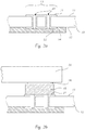
- FIG. 10 shows a circuit board 10 which is structurally similar to circuit board 30 of FIG Fig. 1 is equivalent to.
- the circuit board consists for example of FR-4 material; in the area 13 of a pad, which is provided for a component to be applied to the top side 11 of the circuit board in a later step, there are two thermal vias 20 with a diameter of typically 350 ⁇ m; However, thanks to the invention, larger diameters are also possible, larger vias also being easier to fill and offering a higher overall thermal conductivity.
- the two vias 20 are representative of any number of one, two, three or more thermal vias, the number being able to be selected depending on the application and the desired heat throughput (cooling capacity) to the underside 12.
- thermal vias 20 consist of a known type each of a - usually cylindrical - bore, the inner surface of which is lined with an electrically conductive material - e.g. copper - and a flat area 21 each at the two openings on the top and bottom , 22 passes.
- the area 21 on the upper side 11 and that 22 on the lower side 12 can be the same with regard to the surface shape or (not shown) can be of different sizes.
- a layer 14 of a TIM for example a heat-resistant to the temperatures of the later soldering process, printed on the bottom 12, so that the vias 20 are closed at their lower openings.
- the layer 14 preferably covers the entire area 22 of the vias 20 and can also protrude around the edge of the area 22, thereby electrically isolating the vias on the underside.
- the TIM of the layer 14 is printed over the vias according to the invention, whereby it (for example due to its viscosity) does not penetrate into the vias; the interface between the TIM layer and the underside of a vias is only slightly sickle-shaped (viewed in the longitudinal section).
- the size of an individual area of the printed layer 14 is typically in the region of one square centimeter, these areas as a rule not being over the entire area but being structured.
- solder paste 15 is printed on the upper side of the circuit board and the component 39 including its component pad 38 facing the circuit board 10 is fitted.
- the pad 38 is used here for both the electrical and the thermal Contacting the component 39; in other applications, a pad can only be used for a thermal connection.
- the solder paste is a SnAgCu solder of a type known per se with a silver content of, for example, 3%; a higher proportion of silver can improve the thermal conductivity, but leads to the risk of the formation of an undesirable, brittle Ag 3 Sn phase.
- solder 16 completely fills the vias 20.
- the amount of solder 16 that is required for filling the via can be provided by solder paste extensions on the upper side 11 of the circuit board (not shown).
- the TIM layer 14 applied according to the invention to the underside prevents the solder 16 from flowing away onto the underside of the printed circuit board 12, as well as the formation of undesirable gaps or bubbles in the solder 16 that would otherwise (cf. Fig. 1 ) could occur as a result of loss of solder material.
- a heat sink 24 can be applied over the underside 12 of the circuit board 10 on the TIM layer 14, which additionally improves the heat transfer e.g. to the cooling air or (not shown) a cooling medium due to its shape.
- the heat sink 24 can be applied directly to the TIM layer 14 or by means of an adhesive layer (not shown), it being possible for a fastening by means of a screw connection 23 or the like to be provided for mechanical fixing.
- Fig. 3 shows the obtained circuit arrangement 40 of the exemplary embodiment.
- the exemplary embodiment shown is not to be understood as limiting the invention, but merely serves to illustrate the invention, which extends to a large number of possible embodiments.
- the filled vias have a thermal resistance R th , which is typically about 2/3 of the thermal resistance R. th 0 of the corresponding unfilled Is vias and can be further reduced by increasing the cross-sectional area of the vias.
- the TIM used in the exemplary embodiment preferably has a dielectric strength of 20 to 30 kV / mm. Such a value of the dielectric strength is favorable in order to achieve sufficient mutual electrical insulation of components on the circuit board without further insulation from the heat sink 24, for example of LEDs connected in series in an LED circuit board of a headlight.
- the high thermal conductivity of the TIM allows it to be applied over the entire surface in the form of layer 14. Therefore only one printing step is necessary. Because the solder 16 in the thermal vias 20 makes thermal contact with the TIM layer 14, the effective cross section of the heat-conducting path increases.
Landscapes
- Engineering & Computer Science (AREA)
- Microelectronics & Electronic Packaging (AREA)
- Manufacturing & Machinery (AREA)
- Physics & Mathematics (AREA)
- Thermal Sciences (AREA)
- Structure Of Printed Boards (AREA)
- Cooling Or The Like Of Electrical Apparatus (AREA)
Claims (6)
- Procédé de fabrication d'un circuit (40) sur une plaque de support (10), dans lequel des composants (39) sont appliqués sur une face supérieure (11) de la plaque de support (10), la plaque de support (10) présentant des vias thermiques (20) qui s'étendent à travers la plaque de support (10) jusqu'à une face inférieure (12) opposée à la face supérieure (11),
caractérisé en ce quea) les vias thermiques (20) sont fermés sur la face inférieure (12) par l'application d'une couche (14) de matériau thermoconducteur et électriquement isolant qui ne pénètre pas dans les vias thermiques (20), puisb) les vias thermiques (20) sont remplies de matériau de soudure (15, 16) de la face supérieure (11). - Procédé selon la revendication 1, caractérisé en ce que la couche (14) appliquée à l'étape a) couvre l'ouverture de plusieurs vias (20) ensemble sur la face inférieure (12).
- Procédé selon la revendication 1 ou 2, caractérisé en ce que les vias thermiques (20) dans l'étape a) restent libres au moins en grande partie dans leurs régions entre les faces inférieure et supérieure et ne sont remplies que dans l'étape b).
- Procédé selon l'une quelconque des revendications précédentes, caractérisé en ce que l'étape b) est réalisée par un procédé de brasage à température élevée, de préférence un procédé de refusion.
- Procédé selon l'une quelconque des revendications précédentes, caractérisé en ce qu'après l'étape a) et encore avant l'étape b), une pâte à souder (15) est appliquée sur les vias thermiques (20) sur la face supérieure (11) et ensuite les composants (39) sont montés.
- Utilisation du procédé selon l'une quelconque des revendications précédentes dans la fabrication d'une carte de circuit imprimé d'un projecteur de véhicule, la carte de circuit imprimé comprenant une plaque de support (10) avec au moins un via thermique (20) situé dans la région d'une plage de connexion d'un composant générateur de lumière (39).
Applications Claiming Priority (1)
| Application Number | Priority Date | Filing Date | Title |
|---|---|---|---|
| ATA50934/2014A AT516724B1 (de) | 2014-12-22 | 2014-12-22 | Herstellen einer schaltungsanordnung mit thermischen durchkontaktierungen |
Publications (2)
| Publication Number | Publication Date |
|---|---|
| EP3038436A1 EP3038436A1 (fr) | 2016-06-29 |
| EP3038436B1 true EP3038436B1 (fr) | 2021-10-20 |
Family
ID=54754545
Family Applications (1)
| Application Number | Title | Priority Date | Filing Date |
|---|---|---|---|
| EP15197167.8A Active EP3038436B1 (fr) | 2014-12-22 | 2015-12-01 | Fabrication d'un systeme de commutation comprenant des trous metallises |
Country Status (3)
| Country | Link |
|---|---|
| EP (1) | EP3038436B1 (fr) |
| CN (1) | CN105722308B (fr) |
| AT (1) | AT516724B1 (fr) |
Families Citing this family (6)
| Publication number | Priority date | Publication date | Assignee | Title |
|---|---|---|---|---|
| JP6591673B2 (ja) * | 2016-07-08 | 2019-10-16 | 日立オートモティブシステムズ株式会社 | 電力変換装置 |
| AT520301B1 (de) * | 2017-10-12 | 2019-03-15 | Zkw Group Gmbh | Verfahren zum erzeugen einer leiterplatte mit thermischen durchkontaktierungen, sowie leiterplatte |
| EP3562279A1 (fr) * | 2018-04-25 | 2019-10-30 | Siemens Aktiengesellschaft | Fabrication d'une connexion électrique de composants avec une plaque de contact |
| CZ34499U1 (cs) * | 2020-08-17 | 2020-11-03 | MGM COMPRO s.r.o. | Výkonový regulátor |
| DE102021114658A1 (de) | 2021-06-08 | 2022-12-08 | Continental Automotive Gmbh | Leiterplatte für ein Leistungshalbleitermodul, Leistungshalbleitermodul sowie Verfahren zur Herstellung einer Leiterplatte und eines Leistungshalbleitermoduls |
| EP4456687A1 (fr) * | 2023-04-28 | 2024-10-30 | ZKW Group GmbH | Système de composants |
Citations (1)
| Publication number | Priority date | Publication date | Assignee | Title |
|---|---|---|---|---|
| DE4107312A1 (de) * | 1991-03-07 | 1992-09-10 | Telefunken Electronic Gmbh | Montageanordnung von halbleiterbauelementen auf einer leiterplatte |
Family Cites Families (5)
| Publication number | Priority date | Publication date | Assignee | Title |
|---|---|---|---|---|
| EP0869704A1 (fr) * | 1997-03-31 | 1998-10-07 | Ford Motor Company | Procédé de montage de composants sur une plaque à circuits imprimés |
| DE19842590A1 (de) * | 1998-09-17 | 2000-04-13 | Daimler Chrysler Ag | Verfahren zur Herstellung von Schaltungsanordnungen |
| DE19909505C2 (de) * | 1999-03-04 | 2001-11-15 | Daimler Chrysler Ag | Verfahren zur Herstellung von Schaltungsanordnungen |
| DE10101359A1 (de) * | 2001-01-13 | 2002-07-25 | Conti Temic Microelectronic | Verfahren zur Herstellung einer elektronischen Baugruppe |
| US8166650B2 (en) * | 2008-05-30 | 2012-05-01 | Steering Solutions IP Holding Company | Method of manufacturing a printed circuit board |
-
2014
- 2014-12-22 AT ATA50934/2014A patent/AT516724B1/de active
-
2015
- 2015-12-01 EP EP15197167.8A patent/EP3038436B1/fr active Active
- 2015-12-22 CN CN201510966149.XA patent/CN105722308B/zh active Active
Patent Citations (1)
| Publication number | Priority date | Publication date | Assignee | Title |
|---|---|---|---|---|
| DE4107312A1 (de) * | 1991-03-07 | 1992-09-10 | Telefunken Electronic Gmbh | Montageanordnung von halbleiterbauelementen auf einer leiterplatte |
Also Published As
| Publication number | Publication date |
|---|---|
| EP3038436A1 (fr) | 2016-06-29 |
| CN105722308A (zh) | 2016-06-29 |
| AT516724B1 (de) | 2016-08-15 |
| CN105722308B (zh) | 2019-05-28 |
| AT516724A4 (de) | 2016-08-15 |
Similar Documents
| Publication | Publication Date | Title |
|---|---|---|
| DE102009055691B4 (de) | Leistungshalbleitermodul | |
| EP3036761B1 (fr) | Procédé de soudage par diffusion d'un composant électronique avec une surface de montage avec des enfoncements sur un substrat | |
| AT516724B1 (de) | Herstellen einer schaltungsanordnung mit thermischen durchkontaktierungen | |
| DE19532992A1 (de) | Leiterplatte | |
| EP3698400B1 (fr) | Procédé de fabrication d'un dissipateur thermique sur un module électronique | |
| EP3695691B1 (fr) | Procédé de génération d'une carte de circuit imprimé avec des trous d'interconnexion thermique, ainsi que carte de circuit imprimé | |
| DE102018213859A1 (de) | Leistungshalbleitermodul | |
| EP1445799A2 (fr) | Dispositif à dissipation de chaleur pour un semi-conducteur sur un circuit imprimé | |
| DE102007008912A1 (de) | Halbleitervorrichtung | |
| EP1929847B1 (fr) | Carte de circuits imprimes | |
| DE102007021073B4 (de) | Verfahren zum Herstellen einer Schaltungsanordnung | |
| DE102017208973A1 (de) | Elektronische baugruppe für beleuchtungsanwendungen, beleuchtungseinrichtung sowie verfahren zur herstellung einer elektronischen baugruppe | |
| DE102020200196A1 (de) | Halbleitervorrichtung | |
| DE102015200031A1 (de) | Platine und elektronische vorrichtung | |
| EP3581005B1 (fr) | Dispositif électrique et procédé de fabrication d'un dispositif électrique | |
| WO2009121697A1 (fr) | Composant électroconducteur doté d’un support, de pistes conductrices et de plaquettes conductrices | |
| DE102015204915B4 (de) | Wärmeleitkörper mit einer Koppeloberfläche mit Vertiefung und Wärmetransfervorrichtung | |
| DE102004016847A1 (de) | Leuchtdiodenanordnung und Verfahren zum Herstellen einer Leuchtdiodenanordnung | |
| WO2017001108A1 (fr) | Porte-circuits pour un circuit électronique et procédé de fabrication d'un porte-circuits de ce type | |
| EP3718136B1 (fr) | Ensemble semi-conducteur et procédé de fabrication de l'ensemble semi-conducteur | |
| EP3289619B1 (fr) | Module à del avec dissipation de chaleur améliorée | |
| EP3432692A1 (fr) | Couplage thermique de surfaces de distribution de chaleur en cuivre | |
| DE102009014852A1 (de) | Baugruppe mit einem Kühlelement, Kühlelement für eine derartige Baugruppe und Verfahren zur Herstellung eines derartigen Kühlelements | |
| DE102017207329A1 (de) | Elektronische Baugruppe mit einem zwischen zwei Substraten eingebauten Bauelement und Verfahren zu dessen Herstellung | |
| DE102016202171A1 (de) | Leiterplattenanordnung mit einem abstandshalter zwischen einer platine und einem kühlkörper sowie verfahren und verwendung hierzu |
Legal Events
| Date | Code | Title | Description |
|---|---|---|---|
| PUAI | Public reference made under article 153(3) epc to a published international application that has entered the european phase |
Free format text: ORIGINAL CODE: 0009012 |
|
| AK | Designated contracting states |
Kind code of ref document: A1 Designated state(s): AL AT BE BG CH CY CZ DE DK EE ES FI FR GB GR HR HU IE IS IT LI LT LU LV MC MK MT NL NO PL PT RO RS SE SI SK SM TR |
|
| AX | Request for extension of the european patent |
Extension state: BA ME |
|
| RAP1 | Party data changed (applicant data changed or rights of an application transferred) |
Owner name: ZKW GROUP GMBH |
|
| STAA | Information on the status of an ep patent application or granted ep patent |
Free format text: STATUS: REQUEST FOR EXAMINATION WAS MADE |
|
| 17P | Request for examination filed |
Effective date: 20161223 |
|
| RBV | Designated contracting states (corrected) |
Designated state(s): AL AT BE BG CH CY CZ DE DK EE ES FI FR GB GR HR HU IE IS IT LI LT LU LV MC MK MT NL NO PL PT RO RS SE SI SK SM TR |
|
| STAA | Information on the status of an ep patent application or granted ep patent |
Free format text: STATUS: EXAMINATION IS IN PROGRESS |
|
| 17Q | First examination report despatched |
Effective date: 20181115 |
|
| GRAP | Despatch of communication of intention to grant a patent |
Free format text: ORIGINAL CODE: EPIDOSNIGR1 |
|
| STAA | Information on the status of an ep patent application or granted ep patent |
Free format text: STATUS: GRANT OF PATENT IS INTENDED |
|
| RIC1 | Information provided on ipc code assigned before grant |
Ipc: H05K 3/34 20060101ALN20210428BHEP Ipc: H05K 3/12 20060101ALN20210428BHEP Ipc: H05K 1/11 20060101ALN20210428BHEP Ipc: H05K 3/00 20060101ALI20210428BHEP Ipc: H05K 1/02 20060101AFI20210428BHEP |
|
| INTG | Intention to grant announced |
Effective date: 20210526 |
|
| GRAS | Grant fee paid |
Free format text: ORIGINAL CODE: EPIDOSNIGR3 |
|
| GRAA | (expected) grant |
Free format text: ORIGINAL CODE: 0009210 |
|
| STAA | Information on the status of an ep patent application or granted ep patent |
Free format text: STATUS: THE PATENT HAS BEEN GRANTED |
|
| AK | Designated contracting states |
Kind code of ref document: B1 Designated state(s): AL AT BE BG CH CY CZ DE DK EE ES FI FR GB GR HR HU IE IS IT LI LT LU LV MC MK MT NL NO PL PT RO RS SE SI SK SM TR |
|
| REG | Reference to a national code |
Ref country code: GB Ref legal event code: FG4D Free format text: NOT ENGLISH |
|
| REG | Reference to a national code |
Ref country code: CH Ref legal event code: EP |
|
| REG | Reference to a national code |
Ref country code: DE Ref legal event code: R096 Ref document number: 502015015312 Country of ref document: DE |
|
| REG | Reference to a national code |
Ref country code: IE Ref legal event code: FG4D Free format text: LANGUAGE OF EP DOCUMENT: GERMAN |
|
| REG | Reference to a national code |
Ref country code: AT Ref legal event code: REF Ref document number: 1440982 Country of ref document: AT Kind code of ref document: T Effective date: 20211115 |
|
| REG | Reference to a national code |
Ref country code: LT Ref legal event code: MG9D |
|
| REG | Reference to a national code |
Ref country code: NL Ref legal event code: MP Effective date: 20211020 |
|
| PG25 | Lapsed in a contracting state [announced via postgrant information from national office to epo] |
Ref country code: RS Free format text: LAPSE BECAUSE OF FAILURE TO SUBMIT A TRANSLATION OF THE DESCRIPTION OR TO PAY THE FEE WITHIN THE PRESCRIBED TIME-LIMIT Effective date: 20211020 Ref country code: LT Free format text: LAPSE BECAUSE OF FAILURE TO SUBMIT A TRANSLATION OF THE DESCRIPTION OR TO PAY THE FEE WITHIN THE PRESCRIBED TIME-LIMIT Effective date: 20211020 Ref country code: FI Free format text: LAPSE BECAUSE OF FAILURE TO SUBMIT A TRANSLATION OF THE DESCRIPTION OR TO PAY THE FEE WITHIN THE PRESCRIBED TIME-LIMIT Effective date: 20211020 Ref country code: BG Free format text: LAPSE BECAUSE OF FAILURE TO SUBMIT A TRANSLATION OF THE DESCRIPTION OR TO PAY THE FEE WITHIN THE PRESCRIBED TIME-LIMIT Effective date: 20220120 |
|
| PG25 | Lapsed in a contracting state [announced via postgrant information from national office to epo] |
Ref country code: IS Free format text: LAPSE BECAUSE OF FAILURE TO SUBMIT A TRANSLATION OF THE DESCRIPTION OR TO PAY THE FEE WITHIN THE PRESCRIBED TIME-LIMIT Effective date: 20220220 Ref country code: SE Free format text: LAPSE BECAUSE OF FAILURE TO SUBMIT A TRANSLATION OF THE DESCRIPTION OR TO PAY THE FEE WITHIN THE PRESCRIBED TIME-LIMIT Effective date: 20211020 Ref country code: PT Free format text: LAPSE BECAUSE OF FAILURE TO SUBMIT A TRANSLATION OF THE DESCRIPTION OR TO PAY THE FEE WITHIN THE PRESCRIBED TIME-LIMIT Effective date: 20220221 Ref country code: PL Free format text: LAPSE BECAUSE OF FAILURE TO SUBMIT A TRANSLATION OF THE DESCRIPTION OR TO PAY THE FEE WITHIN THE PRESCRIBED TIME-LIMIT Effective date: 20211020 Ref country code: NO Free format text: LAPSE BECAUSE OF FAILURE TO SUBMIT A TRANSLATION OF THE DESCRIPTION OR TO PAY THE FEE WITHIN THE PRESCRIBED TIME-LIMIT Effective date: 20220120 Ref country code: NL Free format text: LAPSE BECAUSE OF FAILURE TO SUBMIT A TRANSLATION OF THE DESCRIPTION OR TO PAY THE FEE WITHIN THE PRESCRIBED TIME-LIMIT Effective date: 20211020 Ref country code: LV Free format text: LAPSE BECAUSE OF FAILURE TO SUBMIT A TRANSLATION OF THE DESCRIPTION OR TO PAY THE FEE WITHIN THE PRESCRIBED TIME-LIMIT Effective date: 20211020 Ref country code: HR Free format text: LAPSE BECAUSE OF FAILURE TO SUBMIT A TRANSLATION OF THE DESCRIPTION OR TO PAY THE FEE WITHIN THE PRESCRIBED TIME-LIMIT Effective date: 20211020 Ref country code: GR Free format text: LAPSE BECAUSE OF FAILURE TO SUBMIT A TRANSLATION OF THE DESCRIPTION OR TO PAY THE FEE WITHIN THE PRESCRIBED TIME-LIMIT Effective date: 20220121 Ref country code: ES Free format text: LAPSE BECAUSE OF FAILURE TO SUBMIT A TRANSLATION OF THE DESCRIPTION OR TO PAY THE FEE WITHIN THE PRESCRIBED TIME-LIMIT Effective date: 20211020 |
|
| REG | Reference to a national code |
Ref country code: DE Ref legal event code: R097 Ref document number: 502015015312 Country of ref document: DE |
|
| PG25 | Lapsed in a contracting state [announced via postgrant information from national office to epo] |
Ref country code: SM Free format text: LAPSE BECAUSE OF FAILURE TO SUBMIT A TRANSLATION OF THE DESCRIPTION OR TO PAY THE FEE WITHIN THE PRESCRIBED TIME-LIMIT Effective date: 20211020 Ref country code: SK Free format text: LAPSE BECAUSE OF FAILURE TO SUBMIT A TRANSLATION OF THE DESCRIPTION OR TO PAY THE FEE WITHIN THE PRESCRIBED TIME-LIMIT Effective date: 20211020 Ref country code: RO Free format text: LAPSE BECAUSE OF FAILURE TO SUBMIT A TRANSLATION OF THE DESCRIPTION OR TO PAY THE FEE WITHIN THE PRESCRIBED TIME-LIMIT Effective date: 20211020 Ref country code: MC Free format text: LAPSE BECAUSE OF FAILURE TO SUBMIT A TRANSLATION OF THE DESCRIPTION OR TO PAY THE FEE WITHIN THE PRESCRIBED TIME-LIMIT Effective date: 20211020 Ref country code: EE Free format text: LAPSE BECAUSE OF FAILURE TO SUBMIT A TRANSLATION OF THE DESCRIPTION OR TO PAY THE FEE WITHIN THE PRESCRIBED TIME-LIMIT Effective date: 20211020 Ref country code: DK Free format text: LAPSE BECAUSE OF FAILURE TO SUBMIT A TRANSLATION OF THE DESCRIPTION OR TO PAY THE FEE WITHIN THE PRESCRIBED TIME-LIMIT Effective date: 20211020 Ref country code: CZ Free format text: LAPSE BECAUSE OF FAILURE TO SUBMIT A TRANSLATION OF THE DESCRIPTION OR TO PAY THE FEE WITHIN THE PRESCRIBED TIME-LIMIT Effective date: 20211020 |
|
| REG | Reference to a national code |
Ref country code: CH Ref legal event code: PL |
|
| PLBE | No opposition filed within time limit |
Free format text: ORIGINAL CODE: 0009261 |
|
| STAA | Information on the status of an ep patent application or granted ep patent |
Free format text: STATUS: NO OPPOSITION FILED WITHIN TIME LIMIT |
|
| REG | Reference to a national code |
Ref country code: BE Ref legal event code: MM Effective date: 20211231 |
|
| 26N | No opposition filed |
Effective date: 20220721 |
|
| GBPC | Gb: european patent ceased through non-payment of renewal fee |
Effective date: 20220120 |
|
| PG25 | Lapsed in a contracting state [announced via postgrant information from national office to epo] |
Ref country code: LU Free format text: LAPSE BECAUSE OF NON-PAYMENT OF DUE FEES Effective date: 20211201 Ref country code: IE Free format text: LAPSE BECAUSE OF NON-PAYMENT OF DUE FEES Effective date: 20211201 Ref country code: GB Free format text: LAPSE BECAUSE OF NON-PAYMENT OF DUE FEES Effective date: 20220120 Ref country code: AL Free format text: LAPSE BECAUSE OF FAILURE TO SUBMIT A TRANSLATION OF THE DESCRIPTION OR TO PAY THE FEE WITHIN THE PRESCRIBED TIME-LIMIT Effective date: 20211020 |
|
| PG25 | Lapsed in a contracting state [announced via postgrant information from national office to epo] |
Ref country code: SI Free format text: LAPSE BECAUSE OF FAILURE TO SUBMIT A TRANSLATION OF THE DESCRIPTION OR TO PAY THE FEE WITHIN THE PRESCRIBED TIME-LIMIT Effective date: 20211020 Ref country code: BE Free format text: LAPSE BECAUSE OF NON-PAYMENT OF DUE FEES Effective date: 20211231 |
|
| PG25 | Lapsed in a contracting state [announced via postgrant information from national office to epo] |
Ref country code: LI Free format text: LAPSE BECAUSE OF NON-PAYMENT OF DUE FEES Effective date: 20211231 Ref country code: CH Free format text: LAPSE BECAUSE OF NON-PAYMENT OF DUE FEES Effective date: 20211231 |
|
| REG | Reference to a national code |
Ref country code: AT Ref legal event code: MM01 Ref document number: 1440982 Country of ref document: AT Kind code of ref document: T Effective date: 20211201 |
|
| PG25 | Lapsed in a contracting state [announced via postgrant information from national office to epo] |
Ref country code: AT Free format text: LAPSE BECAUSE OF NON-PAYMENT OF DUE FEES Effective date: 20211201 |
|
| PG25 | Lapsed in a contracting state [announced via postgrant information from national office to epo] |
Ref country code: IT Free format text: LAPSE BECAUSE OF FAILURE TO SUBMIT A TRANSLATION OF THE DESCRIPTION OR TO PAY THE FEE WITHIN THE PRESCRIBED TIME-LIMIT Effective date: 20211020 Ref country code: HU Free format text: LAPSE BECAUSE OF FAILURE TO SUBMIT A TRANSLATION OF THE DESCRIPTION OR TO PAY THE FEE WITHIN THE PRESCRIBED TIME-LIMIT; INVALID AB INITIO Effective date: 20151201 |
|
| PG25 | Lapsed in a contracting state [announced via postgrant information from national office to epo] |
Ref country code: CY Free format text: LAPSE BECAUSE OF FAILURE TO SUBMIT A TRANSLATION OF THE DESCRIPTION OR TO PAY THE FEE WITHIN THE PRESCRIBED TIME-LIMIT Effective date: 20211020 |
|
| P01 | Opt-out of the competence of the unified patent court (upc) registered |
Effective date: 20230528 |
|
| PG25 | Lapsed in a contracting state [announced via postgrant information from national office to epo] |
Ref country code: MK Free format text: LAPSE BECAUSE OF FAILURE TO SUBMIT A TRANSLATION OF THE DESCRIPTION OR TO PAY THE FEE WITHIN THE PRESCRIBED TIME-LIMIT Effective date: 20211020 |
|
| PG25 | Lapsed in a contracting state [announced via postgrant information from national office to epo] |
Ref country code: MT Free format text: LAPSE BECAUSE OF FAILURE TO SUBMIT A TRANSLATION OF THE DESCRIPTION OR TO PAY THE FEE WITHIN THE PRESCRIBED TIME-LIMIT Effective date: 20211020 |
|
| REG | Reference to a national code |
Ref country code: DE Ref legal event code: R084 Ref document number: 502015015312 Country of ref document: DE |
|
| PG25 | Lapsed in a contracting state [announced via postgrant information from national office to epo] |
Ref country code: TR Free format text: LAPSE BECAUSE OF FAILURE TO SUBMIT A TRANSLATION OF THE DESCRIPTION OR TO PAY THE FEE WITHIN THE PRESCRIBED TIME-LIMIT Effective date: 20211020 |
|
| PGFP | Annual fee paid to national office [announced via postgrant information from national office to epo] |
Ref country code: FR Payment date: 20251217 Year of fee payment: 11 |
|
| PGFP | Annual fee paid to national office [announced via postgrant information from national office to epo] |
Ref country code: DE Payment date: 20251222 Year of fee payment: 11 |