EP3039718B1 - Modules solaires à couches minces en partie transparentes - Google Patents
Modules solaires à couches minces en partie transparentes Download PDFInfo
- Publication number
- EP3039718B1 EP3039718B1 EP14777014.3A EP14777014A EP3039718B1 EP 3039718 B1 EP3039718 B1 EP 3039718B1 EP 14777014 A EP14777014 A EP 14777014A EP 3039718 B1 EP3039718 B1 EP 3039718B1
- Authority
- EP
- European Patent Office
- Prior art keywords
- transparent
- solar cell
- contact layer
- surface regions
- structuring
- Prior art date
- Legal status (The legal status is an assumption and is not a legal conclusion. Google has not performed a legal analysis and makes no representation as to the accuracy of the status listed.)
- Active
Links
Images




Classifications
-
- H—ELECTRICITY
- H10—SEMICONDUCTOR DEVICES; ELECTRIC SOLID-STATE DEVICES NOT OTHERWISE PROVIDED FOR
- H10F—INORGANIC SEMICONDUCTOR DEVICES SENSITIVE TO INFRARED RADIATION, LIGHT, ELECTROMAGNETIC RADIATION OF SHORTER WAVELENGTH OR CORPUSCULAR RADIATION
- H10F77/00—Constructional details of devices covered by this subclass
- H10F77/10—Semiconductor bodies
- H10F77/14—Shape of semiconductor bodies; Shapes, relative sizes or dispositions of semiconductor regions within semiconductor bodies
-
- H—ELECTRICITY
- H10—SEMICONDUCTOR DEVICES; ELECTRIC SOLID-STATE DEVICES NOT OTHERWISE PROVIDED FOR
- H10F—INORGANIC SEMICONDUCTOR DEVICES SENSITIVE TO INFRARED RADIATION, LIGHT, ELECTROMAGNETIC RADIATION OF SHORTER WAVELENGTH OR CORPUSCULAR RADIATION
- H10F19/00—Integrated devices, or assemblies of multiple devices, comprising at least one photovoltaic cell covered by group H10F10/00, e.g. photovoltaic modules
- H10F19/30—Integrated devices, or assemblies of multiple devices, comprising at least one photovoltaic cell covered by group H10F10/00, e.g. photovoltaic modules comprising thin-film photovoltaic cells
- H10F19/31—Integrated devices, or assemblies of multiple devices, comprising at least one photovoltaic cell covered by group H10F10/00, e.g. photovoltaic modules comprising thin-film photovoltaic cells having multiple laterally adjacent thin-film photovoltaic cells deposited on the same substrate
- H10F19/33—Patterning processes to connect the photovoltaic cells, e.g. laser cutting of conductive or active layers
-
- H—ELECTRICITY
- H10—SEMICONDUCTOR DEVICES; ELECTRIC SOLID-STATE DEVICES NOT OTHERWISE PROVIDED FOR
- H10F—INORGANIC SEMICONDUCTOR DEVICES SENSITIVE TO INFRARED RADIATION, LIGHT, ELECTROMAGNETIC RADIATION OF SHORTER WAVELENGTH OR CORPUSCULAR RADIATION
- H10F19/00—Integrated devices, or assemblies of multiple devices, comprising at least one photovoltaic cell covered by group H10F10/00, e.g. photovoltaic modules
- H10F19/30—Integrated devices, or assemblies of multiple devices, comprising at least one photovoltaic cell covered by group H10F10/00, e.g. photovoltaic modules comprising thin-film photovoltaic cells
- H10F19/31—Integrated devices, or assemblies of multiple devices, comprising at least one photovoltaic cell covered by group H10F10/00, e.g. photovoltaic modules comprising thin-film photovoltaic cells having multiple laterally adjacent thin-film photovoltaic cells deposited on the same substrate
- H10F19/37—Integrated devices, or assemblies of multiple devices, comprising at least one photovoltaic cell covered by group H10F10/00, e.g. photovoltaic modules comprising thin-film photovoltaic cells having multiple laterally adjacent thin-film photovoltaic cells deposited on the same substrate comprising means for obtaining partial light transmission through the integrated devices, or the assemblies of multiple devices, e.g. partially transparent thin-film photovoltaic modules for windows
-
- H—ELECTRICITY
- H10—SEMICONDUCTOR DEVICES; ELECTRIC SOLID-STATE DEVICES NOT OTHERWISE PROVIDED FOR
- H10F—INORGANIC SEMICONDUCTOR DEVICES SENSITIVE TO INFRARED RADIATION, LIGHT, ELECTROMAGNETIC RADIATION OF SHORTER WAVELENGTH OR CORPUSCULAR RADIATION
- H10F19/00—Integrated devices, or assemblies of multiple devices, comprising at least one photovoltaic cell covered by group H10F10/00, e.g. photovoltaic modules
- H10F19/80—Encapsulations or containers for integrated devices, or assemblies of multiple devices, having photovoltaic cells
- H10F19/804—Materials of encapsulations
-
- H—ELECTRICITY
- H10—SEMICONDUCTOR DEVICES; ELECTRIC SOLID-STATE DEVICES NOT OTHERWISE PROVIDED FOR
- H10F—INORGANIC SEMICONDUCTOR DEVICES SENSITIVE TO INFRARED RADIATION, LIGHT, ELECTROMAGNETIC RADIATION OF SHORTER WAVELENGTH OR CORPUSCULAR RADIATION
- H10F19/00—Integrated devices, or assemblies of multiple devices, comprising at least one photovoltaic cell covered by group H10F10/00, e.g. photovoltaic modules
- H10F19/80—Encapsulations or containers for integrated devices, or assemblies of multiple devices, having photovoltaic cells
- H10F19/807—Double-glass encapsulation, e.g. photovoltaic cells arranged between front and rear glass sheets
-
- H—ELECTRICITY
- H10—SEMICONDUCTOR DEVICES; ELECTRIC SOLID-STATE DEVICES NOT OTHERWISE PROVIDED FOR
- H10F—INORGANIC SEMICONDUCTOR DEVICES SENSITIVE TO INFRARED RADIATION, LIGHT, ELECTROMAGNETIC RADIATION OF SHORTER WAVELENGTH OR CORPUSCULAR RADIATION
- H10F19/00—Integrated devices, or assemblies of multiple devices, comprising at least one photovoltaic cell covered by group H10F10/00, e.g. photovoltaic modules
- H10F19/90—Structures for connecting between photovoltaic cells, e.g. interconnections or insulating spacers
- H10F19/902—Structures for connecting between photovoltaic cells, e.g. interconnections or insulating spacers for series or parallel connection of photovoltaic cells
- H10F19/908—Structures for connecting between photovoltaic cells, e.g. interconnections or insulating spacers for series or parallel connection of photovoltaic cells for back-contact photovoltaic cells
-
- H—ELECTRICITY
- H10—SEMICONDUCTOR DEVICES; ELECTRIC SOLID-STATE DEVICES NOT OTHERWISE PROVIDED FOR
- H10F—INORGANIC SEMICONDUCTOR DEVICES SENSITIVE TO INFRARED RADIATION, LIGHT, ELECTROMAGNETIC RADIATION OF SHORTER WAVELENGTH OR CORPUSCULAR RADIATION
- H10F71/00—Manufacture or treatment of devices covered by this subclass
-
- H—ELECTRICITY
- H10—SEMICONDUCTOR DEVICES; ELECTRIC SOLID-STATE DEVICES NOT OTHERWISE PROVIDED FOR
- H10F—INORGANIC SEMICONDUCTOR DEVICES SENSITIVE TO INFRARED RADIATION, LIGHT, ELECTROMAGNETIC RADIATION OF SHORTER WAVELENGTH OR CORPUSCULAR RADIATION
- H10F77/00—Constructional details of devices covered by this subclass
- H10F77/20—Electrodes
- H10F77/206—Electrodes for devices having potential barriers
- H10F77/211—Electrodes for devices having potential barriers for photovoltaic cells
- H10F77/219—Arrangements for electrodes of back-contact photovoltaic cells
-
- Y—GENERAL TAGGING OF NEW TECHNOLOGICAL DEVELOPMENTS; GENERAL TAGGING OF CROSS-SECTIONAL TECHNOLOGIES SPANNING OVER SEVERAL SECTIONS OF THE IPC; TECHNICAL SUBJECTS COVERED BY FORMER USPC CROSS-REFERENCE ART COLLECTIONS [XRACs] AND DIGESTS
- Y02—TECHNOLOGIES OR APPLICATIONS FOR MITIGATION OR ADAPTATION AGAINST CLIMATE CHANGE
- Y02E—REDUCTION OF GREENHOUSE GAS [GHG] EMISSIONS, RELATED TO ENERGY GENERATION, TRANSMISSION OR DISTRIBUTION
- Y02E10/00—Energy generation through renewable energy sources
- Y02E10/50—Photovoltaic [PV] energy
Definitions
- the invention relates to thin-film solar modules in which a desired partial transparency for the incident light is achieved by deliberately removing certain parts of the non-or only very weakly transparent, photovoltaically active surface.
- transparency is understood to mean the permeability to light in the visible spectral range (380 nm to 780 nm), based on the entire area examined. This means explicitly that the area examined (e.g. a solar module) can have areas that are highly opaque or even completely opaque and more translucent. In this context, partial transparency means that the surface under consideration is transparent to part of the incident light.
- Solar cells will play an important role in future energy generation.
- Thin-film solar modules in particular have advantages in terms of low material consumption and easier mass production.
- Such solar modules are constructed from amorphous or polycrystalline semiconductor materials which can be deposited inexpensively on large-area substrates, in particular glass substrates.
- the most important representatives are solar modules based on cadmium sulfide-cadmium telluride (CdS / CdTe), copper indium diselenide (CIS-CIGS) or amorphous silicon (a-Si).
- Thin-film solar modules consist of several layers that are successively deposited on the substrate and possibly further treated.
- the transparent front contact layer, the non-or only very weakly transparent, photovoltaically active semiconductor layers and the back contact layer are deposited from the substrate (usually glass).
- the back contact layer is not transparent.
- designs with transparent back contact layers are also known.
- the generally non-transparent back contact layer, the non-transparent, photovoltaically active semiconductor layers and the transparent front contact layer are deposited from the substrate.
- the front contact layer usually contains transparent conductive oxides (TCO, transparent conductive oxide), e.g. tin-doped indium oxide (ITO), fluorine-doped tin oxide (FTO) or aluminum-doped zinc oxide (AZO) as well as stannate-like compounds, e.g. cadmium stannate (Cd 2 (SnO 4 )), to use.
- TCO transparent conductive oxides
- ITO tin-doped indium oxide
- FTO fluorine-doped tin oxide
- AZO aluminum-doped zinc oxide
- stannate-like compounds e.g. cadmium stannate (Cd 2 (SnO 4 )
- the photovoltaic conversion of solar energy into electrical energy typically causes voltages of less than 1 volt in the state of the art solar cells.
- several individual solar cells must therefore be connected in series.
- this is preferably done by dividing the active area of the solar module into individual, strip-shaped solar cells. The division is made by so-called structuring strips, each structuring strip preferably consisting of three closely adjacent structuring cuts.
- each partial section cuts through only certain individual layers of the layer sequence of the solar module.
- a suitable arrangement of the partial cuts with respect to one another and, if appropriate, suitable filling of the structuring cuts with conductive or insulating material ensures that the back contact of the one solar cell comes into contact with the front contact layer of the subsequent solar cell and the front and back contacts are cut in front of or behind the contact point , which results in the serial connection of these solar cells.
- This process is also called structuring.
- a thin-film solar module according to the prior art has a plurality of individual solar cells, which preferably extend from one edge to the other edge of the solar module (or to the stripped edges of the solar module).
- the individual strip-shaped solar cells are separated from one another by the structuring strips and connected in series with one another.
- Various methods for structuring are known from the prior art, in which the coating in the area of the structuring strips in the form of individual structuring cuts is generally removed in whole or in part. These are, for example, mechanical processes, laser processing processes, paste writing methods or lift-off techniques (cf. DE 37 12 589 A1 and DE 43 24 318 C1 ).
- the structuring strips preferably run parallel to one another.
- An essential aspect of photovoltaic energy generation is the space required to set up the solar modules. From an economic-ecological point of view, the elevation of the solar modules on roofs and the integration of the solar modules in building facades, especially high-rise facades, are particularly desirable.
- solar modules are designed so that they can perform the function of a typical facade cladding.
- they advantageously produce electrical energy that can be used in the home or fed into the public electrical network.
- Facades especially high-rise facades, are generally subject to special architectural requirements.
- areas of the facade cladding are to be made partially transparent. Even if the facade area does not contain a window, but only in front of a functional room that does not require direct daylight, a certain amount of light may still be desirable.
- Partially transparent facade elements can be advantageous here.
- the US 4,795,500 A. describes a thin film solar module made in the Superstrat configuration described above. After the deposition of the metal back electrode, holes are etched in the back electrode or in the back electrode and the photovoltaically active semiconductor layers in order to increase the transparency of the solar module. The back of the solar module is then closed with a transparent protective layer, for example made of plastic.
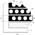
- the object is achieved by producing a partial transparency of the solar module by deliberately removing freely definable surface areas (transparent surface areas) of the layer stack of the thin-film solar cell of such a module in a thin-film solar module using a suitable method, preferably before lamination.
- the freely definable surface areas are preferably designed in such a way that the free areas extend at least through all non-transparent layers, so that a type of window is created in the layer stack of the solar cell through which the light can pass.
- the solar module produced by the method according to the invention has a plurality of freely definable surface areas which do not contain a layer stack or only light-permeable layers of the layer stack.
- the area proportion of the freely definable area areas is preferably between 70% and 5%, particularly preferably between 50% and 10% and very particularly preferably between 40% and 20% of the total area of the solar module. An area share of 30% + -5% has proven to be particularly advantageous.
- the freely definable surface areas are formed by removing all layers of the layer stack, but at least the opaque layers of the layer stack, at each location provided for a surface area.
- the subsequent removal of the layer stack of the thin-film solar cell in the defined surface areas is preferably carried out using a laser method, as is also used in the structuring task of the thin-film module. Also preferred are the mechanical processes mentioned above using gravers and sandblasting effects or special lift-off mechanisms and adapted photolithographic processes.
- the freely definable surface areas are formed by restricting the deposition of all layers of the layer stack, but at least of the opaque layers, to the regions outside the freely definable surface areas.
- Technical precautions from the prior art, such as masks, are suitable for this. With this procedure, the layers are deposited in such a way that defined surface areas (the freely definable surface areas) remain uncoated and partial transparency is achieved in this way.
- the shape of the freely definable surface areas can be arbitrary. However, simple geometric shapes such as rectangles, trapezoids, triangles, polygons or circles will preferably be used. The shapes are chosen so that they can be arranged as symmetrically as possible along a solar cell strip specified by the structuring. The wider the solar cell strips are, the more possibilities there are for the shapes.
- the area proportion of the freely definable area areas in each solar cell strip of a solar cell module is preferably of the same size.
- the transparency is generated by making the structuring cuts wider.
- the freely definable surface areas are filled with a colorless or colored transparent plastic, so that a flat surface is created at the end of the back contact layer.
- a colored plastic advantageous aesthetic embodiments of the solar cell module can be achieved.
- This freely definable surface areas are preferably filled using a photolithographic process according to the prior art.
- PMMA is used as the plastic material.
- the efficiency of the thin-film solar module is ideally reduced only in the ratio of the removed surface to the entire photovoltaically active surface.
- the shapes of the surfaces are preferably selected so that the photovoltaic surfaces obtained have a rectangular shape between the removed surfaces. This ensures that the photovoltaically active residual areas between two adjacent structuring cuts have a constant width b and a rectangular shape. A current path of constant width b of the rectangle is thus available for the photovoltaic current generated in the area regions ⁇ x * b rectangle ( ⁇ x length) along the rectangular photovoltaic residual areas, as in the case of the original solar cell strips.
- Photovoltaically ideal transparent surface areas are therefore rectangles that extend over the entire solar cell strip and are arranged in such a way that the photovoltaically active residual area per solar cell strip is the same for all solar cell strips of the thin-film solar module.
- the dimensions of the freely definable surface areas are selected depending on the intended area of application of the solar cell modules. If the surface equipped with the solar cell modules is to give a smooth and homogeneous impression, the freely definable surface areas are very small, so that the viewer can no longer perceive them individually from a certain distance. In a further preferred embodiment, the freely definable surface areas form their own design elements for the surface to be equipped with the solar cell modules. Here the dimensions are so large that the surface areas are visible to the viewer.
- the photovoltaically active residual areas can be parallelogram-like with the width b of the parallelogram and not meet at the structuring sections over their width b of the parallelogram, but can be arranged laterally offset as desired.
- Circular and elliptical shapes as transparent, photovoltaically inactive surface areas are also preferred.
- transparent trapezoidal and triangular shapes can lead to different widths of photovoltaically active residual areas, depending on the arrangement. Under such circumstances, considerable additional series resistance effects are generated because the current paths become longer than in the original thin-film module and the constrictions of the current paths lead to locally higher current densities with a varying width of the photovoltaically active residual areas. In individual cases, it must be examined or determined by calculation whether the current densities that occur are acceptable or can be compensated for, for example, by increasing the material thickness (layer thickness).
- the process sequence is designed in such a way that the conductive, transparent front contact layer is retained. Because the original current paths of the thin-film solar module are completely preserved for the photovoltaic current generated in the photovoltaically active residual areas in the area of the front contact layer, negative series resistance effects are avoided because no extensions of the current path or undesired local increases in the current density of the photovoltaically generated Current occur.
- the advantageous effect described is particularly important in the case of the front contact layer, because the surface resistance R Square, front of the front contact layer is generally up to a factor of 10 greater than the surface resistance of the back contact R Square, gutter , which is therefore only in the area of photovoltaics active remaining area must be preserved.
- the thickness of the back contact layer can also be increased slightly if series resistance effects occur.
- the thickness of the front contact layer is optimized for photovoltaic effectiveness (transmission of the incident light) and could only be made thicker with additional losses in efficiency.
Landscapes
- Photovoltaic Devices (AREA)
- Life Sciences & Earth Sciences (AREA)
- Engineering & Computer Science (AREA)
- Sustainable Development (AREA)
- Sustainable Energy (AREA)
Claims (6)
- Procédé de fabrication d'un module solaire à couche mince partiellement transparent (10) dans une configuration de substrat, présentant au moins les étapes suivantes :- la préparation d'un substrat (18)- l'application d'une couche de contact arrière transparente ou non transparente (16)- l'application d'une couche semi-conductrice (15) à activité photovoltaïque, à transparence nulle ou très faible- l'application d'une couche de contact avant transparente (14)- la structuration des couches au moyen de bandes structurantes parallèles les unes aux autres et la division du revêtement en bandes de cellules solaires individuelles connectées en série (20)caractérisé en ce que- des zones de surface définies (19, 22) sont éliminées de la couche de contact arrière (16) et de la couche semi-conductrice (15) avant le dépôt de la couche de contact avant (14)- les zones de surface éliminées (19, 22) sont remplies d'un plastique transparent ou transparent coloré, et la couche de contact avant transparente (14) est ensuite déposée sur les zones de surface transparentes et non transparentes (19, 22 ; 21).
- Procédé selon la revendication 1, caractérisé en ce que les zones de surface transparentes (19, 22) sont disposées stochastiquement ou régulièrement sur la surface du module.
- Procédé selon l'une quelconque des revendications précédentes, caractérisé en ce que les zones de surface transparentes (19, 22), de préférence,- sont disposées symétriquement le long des bandes de cellules solaires (20),- leur dimension respective ne dépasse pas la largeur de la bande de cellules solaires (20),- la surface totale des zones de surface transparentes (19, 22) est la même pour toutes les bandes de cellules solaires (20).
- Procédé selon l'une quelconque des revendications précédentes, caractérisé en ce que les zones de surface définies (19, 22) à couche semi-conductrice et couche de contact arrière éliminées (15, 16) sont générées par des sections structurantes élargies à volonté et ainsi la transparence partielle souhaitée est réalisée.
- Procédé selon l'une quelconque des revendications précédentes, caractérisé en ce que les zones de surface définies (19, 22) à couche semi-conductrice et couche de contact arrière éliminées (15, 16) sont situées dans la zone des bandes de cellules solaires (20) et présentent- une forme rectangulaire- une forme parallélogrammatique- une forme circulaire- une forme triangulaire- une forme trapézoïdale- des formes polygonales.
- Procédé selon l'une quelconque des revendications précédentes, caractérisé en ce que les zones de surface définies (19, 22) dans la couche semi-conductrice et la couche de contact arrière (15, 16) sont éliminées à l'aide d'un- processus laser,- processus de rainurage mécanique,- processus de décollage,- processus de gravure,- processus de sablage.
Applications Claiming Priority (2)
| Application Number | Priority Date | Filing Date | Title |
|---|---|---|---|
| CN201310613095.XA CN104425637A (zh) | 2013-08-30 | 2013-08-30 | 部分透明的薄层太阳能模块 |
| PCT/EP2014/068192 WO2015028519A1 (fr) | 2013-08-30 | 2014-08-27 | Modules solaires à couches minces en partie transparentes |
Publications (2)
| Publication Number | Publication Date |
|---|---|
| EP3039718A1 EP3039718A1 (fr) | 2016-07-06 |
| EP3039718B1 true EP3039718B1 (fr) | 2020-04-22 |
Family
ID=51627258
Family Applications (1)
| Application Number | Title | Priority Date | Filing Date |
|---|---|---|---|
| EP14777014.3A Active EP3039718B1 (fr) | 2013-08-30 | 2014-08-27 | Modules solaires à couches minces en partie transparentes |
Country Status (5)
| Country | Link |
|---|---|
| US (1) | US20160276510A1 (fr) |
| EP (1) | EP3039718B1 (fr) |
| CN (1) | CN104425637A (fr) |
| ES (1) | ES2804303T3 (fr) |
| WO (1) | WO2015028519A1 (fr) |
Families Citing this family (3)
| Publication number | Priority date | Publication date | Assignee | Title |
|---|---|---|---|---|
| FR3045945B1 (fr) * | 2015-12-16 | 2017-12-15 | Sunpartner Technologies | Dispositif optique pour diminuer la visibilite des interconnexions electriques dans des modules photovoltaiques semi-transparents en couches minces |
| CN108604618B (zh) * | 2016-12-27 | 2022-12-06 | 中国建材国际工程集团有限公司 | 用于监视在太阳能模块中形成隔离槽的激光划片过程的方法和系统 |
| DE202022000302U1 (de) | 2022-02-05 | 2022-02-22 | Rudi Danz | Semitransparente Solarmodule und ihre Anwendungen |
Citations (1)
| Publication number | Priority date | Publication date | Assignee | Title |
|---|---|---|---|---|
| US20110017280A1 (en) * | 2008-02-07 | 2011-01-27 | Philip Thomas Rumsby | Partially transparent solar panel |
Family Cites Families (17)
| Publication number | Priority date | Publication date | Assignee | Title |
|---|---|---|---|---|
| US4795500A (en) * | 1985-07-02 | 1989-01-03 | Sanyo Electric Co., Ltd. | Photovoltaic device |
| DE3712589A1 (de) | 1987-04-14 | 1988-11-03 | Nukem Gmbh | Verfahren zur herstellung von in reihe verschalteten duennschicht-solarzellen |
| GB2260220B (en) * | 1991-09-10 | 1996-01-03 | Sanyo Electric Co | An amorphous silicon solar cell and method of the solar cell manufacture |
| DE4324318C1 (de) | 1993-07-20 | 1995-01-12 | Siemens Ag | Verfahren zur Serienverschaltung einer integrierten Dünnfilmsolarzellenanordnung |
| JP2000223727A (ja) * | 1999-01-28 | 2000-08-11 | Fuji Electric Co Ltd | 薄膜太陽電池とその製造方法 |
| JP2003305577A (ja) * | 2002-04-11 | 2003-10-28 | Sharp Corp | レーザ加工装置、それを用いた半導体素子の製造方法およびそれを用いた太陽電池素子の製造方法 |
| JPWO2004064167A1 (ja) * | 2003-01-10 | 2006-05-18 | 株式会社カネカ | 透光性薄膜太陽電池モジュールおよびその製造方法 |
| JP4448371B2 (ja) * | 2004-04-19 | 2010-04-07 | シャープ株式会社 | 光源一体型太陽電池モジュールおよびそれを用いた発電発光ユニット |
| DE102004057663B4 (de) * | 2004-09-15 | 2015-08-20 | Sunways Ag | Solarmodul mit durch regulär angeordnete Löcher semitransparenten kristallinen Solarzellen und Verfahren zur Herstellung |
| GB2446838A (en) * | 2007-02-20 | 2008-08-27 | David John Ruchat | Photovoltaic device and manufacturing method |
| TWI379425B (en) * | 2007-12-13 | 2012-12-11 | Nexpower Technology Corp | Translucent solar cell and manufacturing method thereof |
| KR101161378B1 (ko) * | 2008-09-09 | 2012-07-02 | 엘지전자 주식회사 | 백색 반사층을 구비한 박막형 태양전지 모듈 및 그 제조방법 |
| DE102009022378B4 (de) * | 2009-05-23 | 2013-02-07 | Solarion Ag Photovoltaik | Verfahren zur Herstellung von teiltransparenten flexiblen Dünnschichtsolarzellen und teiltransparente flexible Dünnschichtsolarzelle |
| CN101958361A (zh) * | 2009-07-13 | 2011-01-26 | 无锡尚德太阳能电力有限公司 | 透光薄膜太阳电池组件刻蚀方法 |
| GB2472608B (en) * | 2009-08-12 | 2013-09-04 | M Solv Ltd | Method and Apparatus for making a solar panel that is partially transparent |
| JP5325139B2 (ja) * | 2010-02-19 | 2013-10-23 | 東レエンジニアリング株式会社 | 太陽電池モジュール |
| TW201248876A (en) * | 2011-05-17 | 2012-12-01 | Axuntek Solar Energy | See-through solar battery module and manufacturing method thereof |
-
2013
- 2013-08-30 CN CN201310613095.XA patent/CN104425637A/zh active Pending
-
2014
- 2014-08-27 WO PCT/EP2014/068192 patent/WO2015028519A1/fr not_active Ceased
- 2014-08-27 EP EP14777014.3A patent/EP3039718B1/fr active Active
- 2014-08-27 US US14/915,104 patent/US20160276510A1/en not_active Abandoned
- 2014-08-27 ES ES14777014T patent/ES2804303T3/es active Active
Patent Citations (1)
| Publication number | Priority date | Publication date | Assignee | Title |
|---|---|---|---|---|
| US20110017280A1 (en) * | 2008-02-07 | 2011-01-27 | Philip Thomas Rumsby | Partially transparent solar panel |
Also Published As
| Publication number | Publication date |
|---|---|
| EP3039718A1 (fr) | 2016-07-06 |
| WO2015028519A1 (fr) | 2015-03-05 |
| CN104425637A (zh) | 2015-03-18 |
| US20160276510A1 (en) | 2016-09-22 |
| ES2804303T3 (es) | 2021-02-05 |
Similar Documents
| Publication | Publication Date | Title |
|---|---|---|
| DE60222004T2 (de) | Transparentes substrat beschichtet mit einer elektrode | |
| DE69730337T2 (de) | Photovoltaische folie und verfahren zu deren herstellung | |
| DE10017610C2 (de) | Verfahren zur Herstellung eines Solarmoduls mit integriert serienverschalteten Dünnschicht-Solarzellen und Verwendung davon | |
| DE69228079T2 (de) | Photovoltaische Vorrichtung und Solarmodul mit teilweiser Durchsichtigkeit, und Herstellungsmethode | |
| EP2537065B1 (fr) | Vitrage électrochrome doté de cellules connectées en série, ainsi que son procédé de fabrication | |
| DE102017203105B4 (de) | Verglasungseinheit, Verfahren zu deren Herstellung und deren Verwendung | |
| EP2179426B1 (fr) | Système multicouche comprenant des éléments de contact et procédé de production d'un élément de contact pour un système multicouche | |
| DE102009041941A1 (de) | Dünnschichttyp-Solarzelle und Verfahren zum Herstellen derselben | |
| EP2758993B1 (fr) | Module solaire à couches minces à câblage en série et procédé de câblage en série de cellules solaires à couches minces | |
| DE102013220802A1 (de) | Solarmodul und Verfahren zum Herstellen eines Solarmoduls | |
| DE19713215A1 (de) | Solarzelle mit texturierter TCO-Schicht sowie Verfahren zur Herstellung einer solchen TCO-Schicht für eine solche Solarzelle | |
| DE102014200956A1 (de) | Photovoltaische Zelle, Photovoltaikmodul sowie dessen Herstellung und Verwendung | |
| EP3039718B1 (fr) | Modules solaires à couches minces en partie transparentes | |
| CN104823284A (zh) | 薄层光伏装置,特别是用于太阳能窗玻璃的薄层光伏装置 | |
| DE202021003960U1 (de) | Eine Dünnschichtsolarzelle | |
| DE102011010131A1 (de) | Rohmodul zur Herstellung eines Dünnschichtsolarmoduls und Dünnschichtsolarmodul | |
| DE102008050332A1 (de) | Photovoltaische Zellen sowie Mehrschichtfolie | |
| EP1638150A2 (fr) | Module de cellules solaires | |
| AT512678B1 (de) | Photovoltaik Fenster- und/oder Fassadenelement | |
| DE3382695T2 (de) | Fotovoltaischer wandler. | |
| DE102016125637A1 (de) | Photovoltaik-Modul und Verfahren zur Herstellung eines Photovoltaik-Moduls | |
| DE202010013136U1 (de) | Dünnschicht-Photovoltaikmodul | |
| WO2013045147A1 (fr) | Module solaire semi-transparent et élément de vitrage | |
| DE102010017246A1 (de) | Solarzellenmodul und Herstellungsverfahren hierfür | |
| DE102014216792A1 (de) | Verfahren zum Erzeugen einer transparenten Elektrode eines optoelektronischen Bauelementes |
Legal Events
| Date | Code | Title | Description |
|---|---|---|---|
| PUAI | Public reference made under article 153(3) epc to a published international application that has entered the european phase |
Free format text: ORIGINAL CODE: 0009012 |
|
| 17P | Request for examination filed |
Effective date: 20160226 |
|
| AK | Designated contracting states |
Kind code of ref document: A1 Designated state(s): AL AT BE BG CH CY CZ DE DK EE ES FI FR GB GR HR HU IE IS IT LI LT LU LV MC MK MT NL NO PL PT RO RS SE SI SK SM TR |
|
| AX | Request for extension of the european patent |
Extension state: BA ME |
|
| DAX | Request for extension of the european patent (deleted) | ||
| STAA | Information on the status of an ep patent application or granted ep patent |
Free format text: STATUS: EXAMINATION IS IN PROGRESS |
|
| 17Q | First examination report despatched |
Effective date: 20181106 |
|
| GRAP | Despatch of communication of intention to grant a patent |
Free format text: ORIGINAL CODE: EPIDOSNIGR1 |
|
| STAA | Information on the status of an ep patent application or granted ep patent |
Free format text: STATUS: GRANT OF PATENT IS INTENDED |
|
| INTG | Intention to grant announced |
Effective date: 20191119 |
|
| GRAS | Grant fee paid |
Free format text: ORIGINAL CODE: EPIDOSNIGR3 |
|
| GRAA | (expected) grant |
Free format text: ORIGINAL CODE: 0009210 |
|
| STAA | Information on the status of an ep patent application or granted ep patent |
Free format text: STATUS: THE PATENT HAS BEEN GRANTED |
|
| AK | Designated contracting states |
Kind code of ref document: B1 Designated state(s): AL AT BE BG CH CY CZ DE DK EE ES FI FR GB GR HR HU IE IS IT LI LT LU LV MC MK MT NL NO PL PT RO RS SE SI SK SM TR |
|
| REG | Reference to a national code |
Ref country code: CH Ref legal event code: EP |
|
| REG | Reference to a national code |
Ref country code: IE Ref legal event code: FG4D Free format text: LANGUAGE OF EP DOCUMENT: GERMAN |
|
| REG | Reference to a national code |
Ref country code: DE Ref legal event code: R096 Ref document number: 502014014048 Country of ref document: DE |
|
| REG | Reference to a national code |
Ref country code: AT Ref legal event code: REF Ref document number: 1261273 Country of ref document: AT Kind code of ref document: T Effective date: 20200515 |
|
| RAP2 | Party data changed (patent owner data changed or rights of a patent transferred) |
Owner name: CTF SOLAR GMBH Owner name: CHINA TRIUMPH INTERNATIONAL ENGINEERING CO., LTD. |
|
| REG | Reference to a national code |
Ref country code: NL Ref legal event code: FP |
|
| REG | Reference to a national code |
Ref country code: LT Ref legal event code: MG4D |
|
| RAP2 | Party data changed (patent owner data changed or rights of a patent transferred) |
Owner name: CTF SOLAR GMBH Owner name: CHINA TRIUMPH INTERNATIONAL ENGINEERING CO., LTD. |
|
| PG25 | Lapsed in a contracting state [announced via postgrant information from national office to epo] |
Ref country code: LT Free format text: LAPSE BECAUSE OF FAILURE TO SUBMIT A TRANSLATION OF THE DESCRIPTION OR TO PAY THE FEE WITHIN THE PRESCRIBED TIME-LIMIT Effective date: 20200422 Ref country code: NO Free format text: LAPSE BECAUSE OF FAILURE TO SUBMIT A TRANSLATION OF THE DESCRIPTION OR TO PAY THE FEE WITHIN THE PRESCRIBED TIME-LIMIT Effective date: 20200722 Ref country code: GR Free format text: LAPSE BECAUSE OF FAILURE TO SUBMIT A TRANSLATION OF THE DESCRIPTION OR TO PAY THE FEE WITHIN THE PRESCRIBED TIME-LIMIT Effective date: 20200723 Ref country code: PT Free format text: LAPSE BECAUSE OF FAILURE TO SUBMIT A TRANSLATION OF THE DESCRIPTION OR TO PAY THE FEE WITHIN THE PRESCRIBED TIME-LIMIT Effective date: 20200824 Ref country code: FI Free format text: LAPSE BECAUSE OF FAILURE TO SUBMIT A TRANSLATION OF THE DESCRIPTION OR TO PAY THE FEE WITHIN THE PRESCRIBED TIME-LIMIT Effective date: 20200422 Ref country code: IS Free format text: LAPSE BECAUSE OF FAILURE TO SUBMIT A TRANSLATION OF THE DESCRIPTION OR TO PAY THE FEE WITHIN THE PRESCRIBED TIME-LIMIT Effective date: 20200822 Ref country code: SE Free format text: LAPSE BECAUSE OF FAILURE TO SUBMIT A TRANSLATION OF THE DESCRIPTION OR TO PAY THE FEE WITHIN THE PRESCRIBED TIME-LIMIT Effective date: 20200422 |
|
| PG25 | Lapsed in a contracting state [announced via postgrant information from national office to epo] |
Ref country code: HR Free format text: LAPSE BECAUSE OF FAILURE TO SUBMIT A TRANSLATION OF THE DESCRIPTION OR TO PAY THE FEE WITHIN THE PRESCRIBED TIME-LIMIT Effective date: 20200422 Ref country code: RS Free format text: LAPSE BECAUSE OF FAILURE TO SUBMIT A TRANSLATION OF THE DESCRIPTION OR TO PAY THE FEE WITHIN THE PRESCRIBED TIME-LIMIT Effective date: 20200422 Ref country code: LV Free format text: LAPSE BECAUSE OF FAILURE TO SUBMIT A TRANSLATION OF THE DESCRIPTION OR TO PAY THE FEE WITHIN THE PRESCRIBED TIME-LIMIT Effective date: 20200422 Ref country code: BG Free format text: LAPSE BECAUSE OF FAILURE TO SUBMIT A TRANSLATION OF THE DESCRIPTION OR TO PAY THE FEE WITHIN THE PRESCRIBED TIME-LIMIT Effective date: 20200722 |
|
| PG25 | Lapsed in a contracting state [announced via postgrant information from national office to epo] |
Ref country code: AL Free format text: LAPSE BECAUSE OF FAILURE TO SUBMIT A TRANSLATION OF THE DESCRIPTION OR TO PAY THE FEE WITHIN THE PRESCRIBED TIME-LIMIT Effective date: 20200422 |
|
| REG | Reference to a national code |
Ref country code: DE Ref legal event code: R097 Ref document number: 502014014048 Country of ref document: DE |
|
| PG25 | Lapsed in a contracting state [announced via postgrant information from national office to epo] |
Ref country code: CZ Free format text: LAPSE BECAUSE OF FAILURE TO SUBMIT A TRANSLATION OF THE DESCRIPTION OR TO PAY THE FEE WITHIN THE PRESCRIBED TIME-LIMIT Effective date: 20200422 Ref country code: RO Free format text: LAPSE BECAUSE OF FAILURE TO SUBMIT A TRANSLATION OF THE DESCRIPTION OR TO PAY THE FEE WITHIN THE PRESCRIBED TIME-LIMIT Effective date: 20200422 Ref country code: DK Free format text: LAPSE BECAUSE OF FAILURE TO SUBMIT A TRANSLATION OF THE DESCRIPTION OR TO PAY THE FEE WITHIN THE PRESCRIBED TIME-LIMIT Effective date: 20200422 Ref country code: EE Free format text: LAPSE BECAUSE OF FAILURE TO SUBMIT A TRANSLATION OF THE DESCRIPTION OR TO PAY THE FEE WITHIN THE PRESCRIBED TIME-LIMIT Effective date: 20200422 Ref country code: SM Free format text: LAPSE BECAUSE OF FAILURE TO SUBMIT A TRANSLATION OF THE DESCRIPTION OR TO PAY THE FEE WITHIN THE PRESCRIBED TIME-LIMIT Effective date: 20200422 |
|
| REG | Reference to a national code |
Ref country code: ES Ref legal event code: FG2A Ref document number: 2804303 Country of ref document: ES Kind code of ref document: T3 Effective date: 20210205 |
|
| PG25 | Lapsed in a contracting state [announced via postgrant information from national office to epo] |
Ref country code: SK Free format text: LAPSE BECAUSE OF FAILURE TO SUBMIT A TRANSLATION OF THE DESCRIPTION OR TO PAY THE FEE WITHIN THE PRESCRIBED TIME-LIMIT Effective date: 20200422 Ref country code: PL Free format text: LAPSE BECAUSE OF FAILURE TO SUBMIT A TRANSLATION OF THE DESCRIPTION OR TO PAY THE FEE WITHIN THE PRESCRIBED TIME-LIMIT Effective date: 20200422 |
|
| PLBE | No opposition filed within time limit |
Free format text: ORIGINAL CODE: 0009261 |
|
| STAA | Information on the status of an ep patent application or granted ep patent |
Free format text: STATUS: NO OPPOSITION FILED WITHIN TIME LIMIT |
|
| 26N | No opposition filed |
Effective date: 20210125 |
|
| PG25 | Lapsed in a contracting state [announced via postgrant information from national office to epo] |
Ref country code: MC Free format text: LAPSE BECAUSE OF FAILURE TO SUBMIT A TRANSLATION OF THE DESCRIPTION OR TO PAY THE FEE WITHIN THE PRESCRIBED TIME-LIMIT Effective date: 20200422 |
|
| REG | Reference to a national code |
Ref country code: CH Ref legal event code: PL |
|
| PG25 | Lapsed in a contracting state [announced via postgrant information from national office to epo] |
Ref country code: LU Free format text: LAPSE BECAUSE OF NON-PAYMENT OF DUE FEES Effective date: 20200827 Ref country code: LI Free format text: LAPSE BECAUSE OF NON-PAYMENT OF DUE FEES Effective date: 20200831 Ref country code: CH Free format text: LAPSE BECAUSE OF NON-PAYMENT OF DUE FEES Effective date: 20200831 |
|
| REG | Reference to a national code |
Ref country code: BE Ref legal event code: MM Effective date: 20200831 |
|
| PG25 | Lapsed in a contracting state [announced via postgrant information from national office to epo] |
Ref country code: SI Free format text: LAPSE BECAUSE OF FAILURE TO SUBMIT A TRANSLATION OF THE DESCRIPTION OR TO PAY THE FEE WITHIN THE PRESCRIBED TIME-LIMIT Effective date: 20200422 |
|
| PG25 | Lapsed in a contracting state [announced via postgrant information from national office to epo] |
Ref country code: BE Free format text: LAPSE BECAUSE OF NON-PAYMENT OF DUE FEES Effective date: 20200831 Ref country code: IE Free format text: LAPSE BECAUSE OF NON-PAYMENT OF DUE FEES Effective date: 20200827 |
|
| REG | Reference to a national code |
Ref country code: AT Ref legal event code: MM01 Ref document number: 1261273 Country of ref document: AT Kind code of ref document: T Effective date: 20200827 |
|
| PG25 | Lapsed in a contracting state [announced via postgrant information from national office to epo] |
Ref country code: AT Free format text: LAPSE BECAUSE OF NON-PAYMENT OF DUE FEES Effective date: 20200827 |
|
| PG25 | Lapsed in a contracting state [announced via postgrant information from national office to epo] |
Ref country code: TR Free format text: LAPSE BECAUSE OF FAILURE TO SUBMIT A TRANSLATION OF THE DESCRIPTION OR TO PAY THE FEE WITHIN THE PRESCRIBED TIME-LIMIT Effective date: 20200422 Ref country code: MT Free format text: LAPSE BECAUSE OF FAILURE TO SUBMIT A TRANSLATION OF THE DESCRIPTION OR TO PAY THE FEE WITHIN THE PRESCRIBED TIME-LIMIT Effective date: 20200422 Ref country code: CY Free format text: LAPSE BECAUSE OF FAILURE TO SUBMIT A TRANSLATION OF THE DESCRIPTION OR TO PAY THE FEE WITHIN THE PRESCRIBED TIME-LIMIT Effective date: 20200422 |
|
| PG25 | Lapsed in a contracting state [announced via postgrant information from national office to epo] |
Ref country code: MK Free format text: LAPSE BECAUSE OF FAILURE TO SUBMIT A TRANSLATION OF THE DESCRIPTION OR TO PAY THE FEE WITHIN THE PRESCRIBED TIME-LIMIT Effective date: 20200422 |
|
| PGFP | Annual fee paid to national office [announced via postgrant information from national office to epo] |
Ref country code: NL Payment date: 20240829 Year of fee payment: 11 |
|
| PGFP | Annual fee paid to national office [announced via postgrant information from national office to epo] |
Ref country code: GB Payment date: 20240902 Year of fee payment: 11 |
|
| PGFP | Annual fee paid to national office [announced via postgrant information from national office to epo] |
Ref country code: FR Payment date: 20240823 Year of fee payment: 11 |
|
| PGFP | Annual fee paid to national office [announced via postgrant information from national office to epo] |
Ref country code: ES Payment date: 20240918 Year of fee payment: 11 |
|
| PGFP | Annual fee paid to national office [announced via postgrant information from national office to epo] |
Ref country code: IT Payment date: 20240828 Year of fee payment: 11 |
|
| REG | Reference to a national code |
Ref country code: DE Ref legal event code: R079 Ref document number: 502014014048 Country of ref document: DE Free format text: PREVIOUS MAIN CLASS: H01L0027142000 Ipc: H10F0019500000 |
|
| PGFP | Annual fee paid to national office [announced via postgrant information from national office to epo] |
Ref country code: DE Payment date: 20250919 Year of fee payment: 12 |
|
| REG | Reference to a national code |
Ref country code: NL Ref legal event code: MM Effective date: 20250901 |