EP3041032B1 - Composition de formation de film mince de lanio3, et procédé de formation d'un film mince de lanio3 dans lequel ladite composition est utilisée - Google Patents
Composition de formation de film mince de lanio3, et procédé de formation d'un film mince de lanio3 dans lequel ladite composition est utilisée Download PDFInfo
- Publication number
- EP3041032B1 EP3041032B1 EP14853724.4A EP14853724A EP3041032B1 EP 3041032 B1 EP3041032 B1 EP 3041032B1 EP 14853724 A EP14853724 A EP 14853724A EP 3041032 B1 EP3041032 B1 EP 3041032B1
- Authority
- EP
- European Patent Office
- Prior art keywords
- lanio
- film
- thin
- precursor
- forming
- Prior art date
- Legal status (The legal status is an assumption and is not a legal conclusion. Google has not performed a legal analysis and makes no representation as to the accuracy of the status listed.)
- Not-in-force
Links
Images
Classifications
-
- H—ELECTRICITY
- H10—SEMICONDUCTOR DEVICES; ELECTRIC SOLID-STATE DEVICES NOT OTHERWISE PROVIDED FOR
- H10B—ELECTRONIC MEMORY DEVICES
- H10B53/00—Ferroelectric RAM [FeRAM] devices comprising ferroelectric memory capacitors
-
- H—ELECTRICITY
- H01—ELECTRIC ELEMENTS
- H01G—CAPACITORS; CAPACITORS, RECTIFIERS, DETECTORS, SWITCHING DEVICES, LIGHT-SENSITIVE OR TEMPERATURE-SENSITIVE DEVICES OF THE ELECTROLYTIC TYPE
- H01G4/00—Fixed capacitors; Processes of their manufacture
- H01G4/33—Thin- or thick-film capacitors (thin- or thick-film circuits; capacitors without a potential-jump or surface barrier specially adapted for integrated circuits, details thereof, multistep manufacturing processes therefor)
-
- C—CHEMISTRY; METALLURGY
- C09—DYES; PAINTS; POLISHES; NATURAL RESINS; ADHESIVES; COMPOSITIONS NOT OTHERWISE PROVIDED FOR; APPLICATIONS OF MATERIALS NOT OTHERWISE PROVIDED FOR
- C09D—COATING COMPOSITIONS, e.g. PAINTS, VARNISHES OR LACQUERS; FILLING PASTES; CHEMICAL PAINT OR INK REMOVERS; INKS; CORRECTING FLUIDS; WOODSTAINS; PASTES OR SOLIDS FOR COLOURING OR PRINTING; USE OF MATERIALS THEREFOR
- C09D5/00—Coating compositions, e.g. paints, varnishes or lacquers, characterised by their physical nature or the effects produced; Filling pastes
- C09D5/24—Electrically-conducting paints
-
- H—ELECTRICITY
- H01—ELECTRIC ELEMENTS
- H01B—CABLES; CONDUCTORS; INSULATORS; SELECTION OF MATERIALS FOR THEIR CONDUCTIVE, INSULATING OR DIELECTRIC PROPERTIES
- H01B1/00—Conductors or conductive bodies characterised by the conductive materials; Selection of materials as conductors
- H01B1/06—Conductors or conductive bodies characterised by the conductive materials; Selection of materials as conductors mainly consisting of other non-metallic substances
- H01B1/08—Conductors or conductive bodies characterised by the conductive materials; Selection of materials as conductors mainly consisting of other non-metallic substances oxides
-
- H—ELECTRICITY
- H01—ELECTRIC ELEMENTS
- H01G—CAPACITORS; CAPACITORS, RECTIFIERS, DETECTORS, SWITCHING DEVICES, LIGHT-SENSITIVE OR TEMPERATURE-SENSITIVE DEVICES OF THE ELECTROLYTIC TYPE
- H01G4/00—Fixed capacitors; Processes of their manufacture
- H01G4/002—Details
- H01G4/018—Dielectrics
- H01G4/06—Solid dielectrics
- H01G4/08—Inorganic dielectrics
- H01G4/12—Ceramic dielectrics
- H01G4/1272—Semiconductive ceramic capacitors
-
- H—ELECTRICITY
- H10—SEMICONDUCTOR DEVICES; ELECTRIC SOLID-STATE DEVICES NOT OTHERWISE PROVIDED FOR
- H10D—INORGANIC ELECTRIC SEMICONDUCTOR DEVICES
- H10D1/00—Resistors, capacitors or inductors
- H10D1/60—Capacitors
- H10D1/68—Capacitors having no potential barriers
- H10D1/692—Electrodes
-
- H—ELECTRICITY
- H10—SEMICONDUCTOR DEVICES; ELECTRIC SOLID-STATE DEVICES NOT OTHERWISE PROVIDED FOR
- H10N—ELECTRIC SOLID-STATE DEVICES NOT OTHERWISE PROVIDED FOR
- H10N15/00—Thermoelectric devices without a junction of dissimilar materials; Thermomagnetic devices, e.g. using the Nernst-Ettingshausen effect
- H10N15/10—Thermoelectric devices using thermal change of the dielectric constant, e.g. working above and below the Curie point
-
- H—ELECTRICITY
- H10—SEMICONDUCTOR DEVICES; ELECTRIC SOLID-STATE DEVICES NOT OTHERWISE PROVIDED FOR
- H10N—ELECTRIC SOLID-STATE DEVICES NOT OTHERWISE PROVIDED FOR
- H10N30/00—Piezoelectric or electrostrictive devices
- H10N30/01—Manufacture or treatment
- H10N30/06—Forming electrodes or interconnections, e.g. leads or terminals
-
- H—ELECTRICITY
- H10—SEMICONDUCTOR DEVICES; ELECTRIC SOLID-STATE DEVICES NOT OTHERWISE PROVIDED FOR
- H10N—ELECTRIC SOLID-STATE DEVICES NOT OTHERWISE PROVIDED FOR
- H10N30/00—Piezoelectric or electrostrictive devices
- H10N30/80—Constructional details
- H10N30/87—Electrodes or interconnections, e.g. leads or terminals
- H10N30/877—Conductive materials
-
- H—ELECTRICITY
- H10—SEMICONDUCTOR DEVICES; ELECTRIC SOLID-STATE DEVICES NOT OTHERWISE PROVIDED FOR
- H10N—ELECTRIC SOLID-STATE DEVICES NOT OTHERWISE PROVIDED FOR
- H10N30/00—Piezoelectric or electrostrictive devices
- H10N30/80—Constructional details
- H10N30/87—Electrodes or interconnections, e.g. leads or terminals
- H10N30/877—Conductive materials
- H10N30/878—Conductive materials the principal material being non-metallic, e.g. oxide or carbon based
-
- H—ELECTRICITY
- H10—SEMICONDUCTOR DEVICES; ELECTRIC SOLID-STATE DEVICES NOT OTHERWISE PROVIDED FOR
- H10D—INORGANIC ELECTRIC SEMICONDUCTOR DEVICES
- H10D1/00—Resistors, capacitors or inductors
- H10D1/60—Capacitors
- H10D1/68—Capacitors having no potential barriers
- H10D1/682—Capacitors having no potential barriers having dielectrics comprising perovskite structures
Definitions
- the present invention relates to a composition for forming an LaNiO 3 thin-film used in an electrode for a thin-film capacitor, a capacitor for a ferroelectric random access memory (FeRAM), a piezoelectric element or a pyroelectric infrared detecting device by chemical solution deposition (CSD) method, and a method for forming an LaNiO 3 thin-film in which said composition is used. More specifically, the present invention relates to an LaNiO 3 thin-film-forming composition capable of achieving uniform film formation to generate an extremely small number of pinholes, and a method for forming an LaNiO 3 thin-film in which said composition is used.
- This international application claims the priority of Japanese Patent Application No. 2013-214458 filed on October 15, 2013 and Japanese Patent Application No. 2014-202797 filed on October 1, 2014 .
- a conventional type of LaNiO 3 thin-film is formed by vacuum deposition method such as sputtering coating, and by chemical solution deposition (CSD) method such as sol-gel process by applying a sol-gel solution (composition) obtained by dissolving an LaNiO 3 precursor in a solvent to form a coating film and firing the same at a predetermined temperature to be crystallized (see, e.g. Patent Document 1).
- a sol-gel solution (composition) obtained by dissolving an LaNiO 3 precursor in a solvent to form a coating film and firing the same at a predetermined temperature to be crystallized
- a sol-gel solution composition obtained by dissolving an LaNiO 3 precursor in a solvent to form a coating film and firing the same at a predetermined temperature to be crystallized
- a generated coating film is fired at a temperature of 500 to 800°C in oxygen atmosphere. Accordingly, a thin-film composed of metal oxide of a perovskite structure having an LaNiO 3 composition of a film thickness adjusted so that a volume resistivity is 2 ⁇ 10 -5 ⁇ • m or less at a temperature of 20 to 800°C, or a surface resistance is 300 ⁇ / ⁇ or less is obtained.
- the method for producing a transparent conductive thin-film configured in this way is used to efficiently manufacture a transparent conductive thin-film composed of LaNiO 3 of a perovskite structure.
- Patent Document 2 discloses a LaNiO 3 thin film-forming composition
- a LaNiO 3 precursor an organic solvent and a stabilizer.
- the solvent is a diol.
- Preferred diols are 1,3-propanediol, 1,4-butanediol, 1,5-pentanediol and 1,6-hexanediol.
- Patent Document 3 discloses a method for preparing a lanthanum nickelate conductive metal oxide film, wherein LaNO 3 and La acetate are dissolved in ethanol as a solvent.
- Patent Document 4 discloses a similar method wherein acetic acid and deionized water are used as a solvent and methanamide is used as an additive.
- Patent Document 5 discloses a sol gel process for forming a lanthanum nickelate metal oxide film using deionized water, glacial acetic acid and glycol methyl ether as a solvent.
- Patent Document 6 relates to BiNbO 4 ferroelectric films.
- an organic solvent is used, preferably an alcohol.
- a method for forming an LaNiO 3 thin-film by CSD method such as sol-gel process has not unfortunately been firmly established, and distinctive film formation conditions such as the type of solvent contained in a composition and firing temperature can cause various disadvantages.
- a conventional method for producing a transparent conductive thin-film shown in the above Patent Document 1 has a problem that it fails to achieve uniform film formation due to many voids generated on a fired thin-film. This is primarily attributed to many pinholes generated on a coating film just after film formation, with a composition to be used containing a water-soluble component having high surface tension as a solvent. Void generation leads to non-uniform film thickness, resulting in such problems as increased film resistivity.
- inventors of the present invention have found that when an LaNiO 3 thin-film is formed by a sol-gel process, the film has been improved particularly by selecting a material contained in a composition, and consequently pinholes generated on a coating film just after film formation can be reduced, thereby significantly suppressing voids generated on a fired thin-film to achieve uniform film formation. Based on that information, the present invention was accomplished.
- a first aspect of the present invention is an LaNiO 3 thin-film-forming composition, comprising an LaNiO 3 precursor, an organic solvent and a stabilizer, characterized in that the mixture ratio of the LaNiO 3 precursor relative to a total of 100% by mass of the LaNiO 3 precursor, the organic solvent, and the stabilizer is 1 to 20% by mass on an oxide basis, the mixture ratio of the stabilizer relative to ta total amount of the LaNiO 3 precursor (1 mol2) is over 0 moles and 10 moles or less, and the remainder is the organic solvent, the organic solvent is one type of single solvent selected from the group consisting of ethylene glycol monopropyl ether, ethylene glycol monoisopropyl ether, 3-methoxy-1-butanol, hexamethylene tetramine, isoamyl acetate, glycerol 1,2-carbonate, diethyl carbonate, and lactic acid or a mixed solvent composed of ethylene glycol monoisopropylether and ethanol, and
- a second aspect of the present invention is the invention according to the first aspect, wherein the LaNiO 3 precursor is metal carboxylate, metal nitrate, metal alkoxide, a metal diol complex, a metal triol complex, a metal ⁇ -diketonate complex, a metal ⁇ -diketoester complex, a metal ⁇ -iminoketo complex, or a metal amino complex.
- the LaNiO 3 precursor is metal carboxylate, metal nitrate, metal alkoxide, a metal diol complex, a metal triol complex, a metal ⁇ -diketonate complex, a metal ⁇ -diketoester complex, a metal ⁇ -iminoketo complex, or a metal amino complex.
- a third aspect of the present invention is the invention according to the second aspect, wherein at least one of an LaNiO 3 precursor as an La source and an LaNiO 3 precursor as a Ni source is acetate.
- a fourth aspect of the present invention is the invention according to the second aspect, wherein at least one of an LaNiO 3 precursor as an La source and an LaNO 3 precursor as a Ni source is nitrate.
- a fifth aspect of the present invention is a method for forming an LaNiO 3 thin-film in which the LaNiO 3 thin-film-forming composition according to any one of the first to fourth aspects is used.
- a sixth aspect of the present invention is a method for forming an LaNiO 3 thin-film, comprising the steps of:
- a seventh aspect of the present invention is an electronic component including an LaNiO 3 thin-film formed by the method according to the fifth or sixth aspect.
- the LaNiO 3 thin-film-forming composition according to the first aspect of the present invention as defined in claim 1 uses no water-soluble component as a solvent unlike conventional one, and can significantly reduce pinholes generated on a coating film just after film formation by containing an LaNiO 3 precursor and an organic solvent, and fulfilling the above relations of the dispersion component dD, the polarization component dP, and the hydrogen bond component dH of the HSP value of the organic solvent. Additionally, by containing a stabilizer in a composition with the above ratio, storage stability can be improved. Also, containing an LaNiO 3 precursor with a predetermined ratio, cracks generated on a fired LaNiO 3 thin- film can be suppressed, and precipitation (deposition) of an LaNiO 3 precursor can be suppressed.
- the LaNiO 3 thin-film-forming composition according to the second aspect of the present invention can further improve the compositional uniformity of the composition because the LaNiO 3 precursor is metal carboxylate or the like.
- the LaNiO 3 thin-film-forming composition according to the third or fourth aspect of the present invention can further improve the storage stability by using acetate or nitrate as an LaNiO 3 precursor, even if a composition of relatively high concentration is prepared.
- the LaNiO 3 thin-film-forming composition according to the first aspect of the present invention can improve the coating film property because the organic solvent is one type of single solvent selected from the group consisting of ethylene glycol monopropyl ether, ethylene glycol monoisopropyl ether, 3-methoxy-1-butanol, hexamethylene tetramine, isoamyl acetate, glycerol 1, 2-carbonate, diethyl carbonate, and lactic acid, or a mixed solvent composed of ethylene glycol monoisopropylether and ethanol.
- the organic solvent is one type of single solvent selected from the group consisting of ethylene glycol monopropyl ether, ethylene glycol monoisopropyl ether, 3-methoxy-1-butanol, hexamethylene tetramine, isoamyl acetate, glycerol 1, 2-carbonate, diethyl carbonate, and lactic acid, or a mixed solvent composed of ethylene glycol monoisopropy
- the method for forming an LaNiO 3 thin-film according to the fifth aspect of the present invention can form an LaNiO 3 thin-film of uniform thickness having few voids generated after firing derived from an extremely small number of pinholes generated on a coating film just after film formation by forming an LaNiO 3 thin-film by using the above LaNiO 3 thin-film-forming composition.
- the method for forming an LaNiO 3 thin-film according to the sixth aspect of the present invention can form an uniform LaNiO 3 thin-film preferentially oriented to a (100) plane having few voids generated after firing derived from an extremely small number of pinholes generated on a coating film just after film formation by forming a coating film by applying an LaNiO 3 thin-film-forming composition to a heat-resistant substrate, repeatedly forming and calcining the coating film twice or more after calcining the substrate having the coating film at atmospheric pressure in oxidizing atmosphere or in water vapor-containing atmosphere or until the thickness comes to a desired value, and firing the coating film at a crystallization temperature or more.
- the electronic component including the LaNiO 3 thin-film according to the seventh aspect of the present invention can obtain a device excellent in fatigue property by using a uniform thin- film formed by the above method having few voids generated in a capacitor electrode of a ferroelectric memory or a piezoelectric electrode when the ferroelectric memory or a piezoelectric element is manufactured. Also, since the film obtained by the forming method according to the present invention is translucent, the film can be used as an electrode film of a pyroelectric infrared detecting device as well.
- the film can be used as a crystal orientation control layer for controlling crystal orientation of a dielectric layer, particularly when a thin-film capacitor or a piezoelectric element is manufactured.
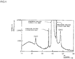
- Fig. 1 is a diagram showing an XRD pattern of an LaNiO 3 thin-film formed in Example 1.
- the composition of the present invention includes an LaNiO 3 precursor, an organic solvent, and a stabilizer. Also, the mixture ratio of the LaNiO 3 precursor relative to a total of 100% by mass of the LaNiO 3 precursor, the organic solvent, and the stabilizer is 1 to 20% by mass on an oxide basis, preferably 3 to 15% by mass. The mixture ratio of the stabilizer relative to a total amount of the LaNiO 3 precursor (1 mole) is over 0 mole and 10 moles or less, and more preferably 2 to 8 moles.
- the dispersion component dD, the polarization component dP, and the hydrogen bond component dH of the HSP value of the organic solvent fulfill the following relations, respectively: 14 ⁇ dD ⁇ 20, preferably 15 ⁇ dD ⁇ 17; 3 ⁇ dP ⁇ 26, preferably 5 ⁇ dP ⁇ 9; and 3 ⁇ dH ⁇ 30, preferably 13 ⁇ dH ⁇ 22.
- the dispersion component dD, the polarization component dP, and the hydrogen bond component dH of the HSP value of the organic solvent can be determined by the values of the evaporation heat, the molecular volume, the refractive index, and the dipole moment.
- d Tot can be determined by the evaporation heat, dP by the dipole moment and the molecular volume, dD by the refractive index, and dH by the above d Tot , dP, and dD.
- d Tot is the sum of dD, dP, and dH.
- the above LaNiO 3 precursor is a raw material for composing composite metal oxide (LaNiO 3 ) in a formed LaNiO 3 thin-film, including metal carboxylate, metal nitrate, metal alkoxide, a metal diol complex, a metal triol complex, a metal ⁇ -diketonate complex, a metal ⁇ -diketoester complex, a metal ⁇ -iminoketo complex or a metal amino complex of each metal element of La or Ni.
- LaNiO 3 precursor as an La source includes: metal carboxylate such as lanthanum acetate, octyl acid lanthanum, and lanthanum 2-ethylhexanoate; metal nitrate such as lanthanum nitrate; metal alkoxide such as lanthanum isopropoxide; and a metal ⁇ -diketonate complex such as lanthanum acetyl acetonate.
- metal carboxylate such as lanthanum acetate, octyl acid lanthanum, and lanthanum 2-ethylhexanoate
- metal nitrate such as lanthanum nitrate
- metal alkoxide such as lanthanum isopropoxide
- a metal ⁇ -diketonate complex such as lanthanum acetyl acetonate.
- LaNiO 3 precursor as a Ni source includes: metal carboxylate such as nickel acetate, octyl acid nickel, and nickel 2-ethylhexoate; metal nitrate such as nickel nitrate; and a metal ⁇ -diketonate complex such as nickel acetylacetonate.
- metal carboxylate such as nickel acetate, octyl acid nickel, and nickel 2-ethylhexoate
- metal nitrate such as nickel nitrate
- a metal ⁇ -diketonate complex such as nickel acetylacetonate.
- at least one of an LaNiO 3 precursor as an La source and an LaNiO 3 precursor as an Ni source is preferably acetate or nitrate.
- the LaNiO 3 precursor is preferably dehydrated by heating means or other means in advance, or dehydrated by distilling means or other means during synthesis of the precursor in view of suppressing pinholes generated on a coating film. If the La source or the Ni source is a hydrate, the LaNiO 3 precursor is essentially dehydrated.
- the mixture ratio of the LaNiO 3 precursor (a total of an La source and a Ni source) relative to a total of 100% by mass of the LaNiO 3 precursor, the organic solvent, and the stabilizer is limited to a range of 1 to 20% by mass on an oxide basis. This is because if the ratio of the LaNiO 3 precursor is under 1% by mass, the thickness of a coated film is too small, resulting in such problems as cracks on a fired LaNiO 3 thin-film, and if the ratio exceeds 20% by mass, degradation of the storage stability such as precipitation (deposition) of an LaNiO 3 precursor is generated.
- the ratio on an oxide basis corresponds to the ratio of the metal oxide relative to a total of 100% by mass of the LaNiO 3 precursor, the organic solvent, and the stabilizer if all the metal elements contained in a composition turn into oxide.
- the mixture ratio of an LaNiO 3 precursor as an La source and an LaNiO 3 precursor as a Ni source is preferably determined so that the metal atomic ratio (La/Ni) of an La element and a Ni element is 1:1.
- the organic solvent for use includes one type of single solvent selected from the group consisting of ethylene glycol monopropyl ether, ethylene glycol monoisopropyl ether, 3-methoxy-1-butanol, hexamethylene tetramine, isoamyl acetate, glycerol 1,2-carbonate, diethyl carbonate, and lactic acid, or a mixed solvent composed of ethylene glycol monoisopropylether and ethanol.
- the HSP value of the organic solvent is Hansen solubility parameter, which refers to the index of how much one substance is dissolved in another substance.
- the Hansen solubility parameter refers to the solubility in the form of three-dimensional vectors (dispersion component dD, polarization component dP, and hydrogen bond component dH). The more approximate the vectors are, the higher solubility is judged.
- the above dispersion component dD is Van der Waals' forces
- the polarization component dP is force of dipole moment
- the hydrogen bond component dH is force found in water or alcohol.
- the dispersion component dD, the polarization component dP, and the hydrogen bond component dH of the HSP value of the organic solvent are limited to the ranges of 14 ⁇ dD ⁇ 20, 3 ⁇ dP ⁇ 26, and 3 ⁇ dH ⁇ 30, respectively. This is because their deviation from each range leads to degraded solubility in the organic solvent of the LaNiO 3 precursor, precipitation of the LaNiO 3 precursor, pinholes generated on a coating film applied to a substrate, or degradation of a coating film property on a substrate of a composition to generate cracks on a fired thin-film.
- the dispersion component dD of the HSP value of the organic solvent is limited to the range of 14 ⁇ dD ⁇ 20, because if the dD is 14 or less or 20 or more, the LaNiO 3 precursor can precipitate.
- the polarization component dP of the HSP value of the organic solvent is limited to the range of 3 ⁇ dP ⁇ 26, because if the dP is 3 or less, the LaNiO 3 precursor can precipitate, and if the dP is 26 or more, pinholes are generated on a coating film of the LaNiO 3 thin-film-forming composition applied to a substrate.
- the hydrogen bond component dH of the HSP value of the organic solvent is limited to the range of 3 ⁇ dH ⁇ 30, because if the dH is 3 or less, the LaNiO 3 precursor can precipitate, and if the dH is 30 or more, pinholes are generated on a coating film of the LaNiO 3 thin-film-forming composition applied to a substrate.
- illustrative preferable example of the stabilizer for use includes one or more types of those selected from the group consisting of ⁇ -diketone (e.g. acetylacetone, heptafluorobutyrylpivaloylmethane, dipivaloyl methane, trifluoroacetylacetone, and benzoylacetone), ⁇ -ketonic acid (e.g. acetoacetic acid, propionyl acetic acid, and benzoyl acetic acid), ⁇ -keto ester (e.g. lower alkylester of methyl, propyl, and butyl of the above ketonic acid), oxyacid (e.g.
- ⁇ -diketone e.g. acetylacetone, heptafluorobutyrylpivaloylmethane, dipivaloyl methane, trifluoroacetylacetone, and benzoylacetone
- ⁇ -ketonic acid e.g.
- lactic acid, glycolic acid, ⁇ -oxybutyric acid, and salicylic acid diol, triol, carboxylic acid, alkanolamine (e.g. diethanolamine, triethanolamine, monoethanolamine, and N-methylformamide), and polyvalent amine.
- alkanolamine e.g. diethanolamine, triethanolamine, monoethanolamine, and N-methylformamide
- polyvalent amine e.g. a composition
- alkanolamine e.g. diethanolamine, triethanolamine, monoethanolamine, and N-methylformamide
- polyvalent amine polyvalent amine.
- alkanolamine such as N-methylformamide and diethanolamine is preferable due to high effect of improving the storage stability.
- the mixture ratio of the stabilizer relative to a total amount of the LaNiO 3 precursor (1 mole) is limited to the range of over 0 mole and 10 moles or less, because there occurs a problem that the ratio of the stabilizer exceeding an upper limit leads to slower thermal decomposition of the stabilizer and cracks generated on a thin-film.
- the ratio of the stabilizer relative to a total amount of the above LaNiO 3 precursor (1 mole) is preferably 2 to 8 moles.
- Illustrative preferable example of the carboxylic acid as a stabilizer includes acetic acid, octylic acid, and 2-ethyl hexanoic acid. If carboxylic acid is used as a stabilizer, the upper limit of the ratio of the above-described stabilizer shows the ratio of carboxylic acid as the stabilizer.
- the above-described LaNiO 3 precursor as an La source and the above-described LaNiO 3 precursor as a Ni source are each prepared, and these are weighed so that the above desired metal atomic ratio can be given.
- the above stabilizer is prepared, and weighed so that the mixture ratio is the above-described predetermined ratio relative to 1 mole of the above LaNiO 3 precursor (a total amount of an LaNiO 3 precursor as an La source and an LaNiO 3 precursor as a Ni source) .
- an LaNiO 3 precursor as a Ni source, the above-described organic solvent, and the above stabilizer are fed into in a reaction vessel and mixed.
- Ni source is a hydrate
- it is distilled for dehydration.
- An LaNiO 3 precursor as an La source is added thereto, and heated and reacted at a temperature of 80 to 200°C for 10 minutes to 2 hours, preferably in atmosphere of inert gas such as nitrogen gas and argon gas to prepare a synthetic liquid (mixed solution).
- inert gas such as nitrogen gas and argon gas
- the La source is a hydrate, it is distilled for dehydration. Thereafter, the above-described organic solvent is further added thereto, and diluted so that the above precursor concentration is in the above-described desired range (weight is adjusted) and agitated to obtain a composition.
- the product is preferably heated at a temperature of 80 to 200°C for 10 minutes to 2 hours, preferably in atmosphere of inert gas such as nitrogen gas and argon gas.
- inert gas such as nitrogen gas and argon gas.
- a stabilizer is added thereto, and heated and reacted at a temperature of 80 to 200°C for 10 minutes to 2 hours in inert gas atmosphere to prepare a synthetic liquid (mixed solution), and an organic solvent may further be added thereto for weight adjustment to obtain a composition.
- particles are preferably removed from the above prepared composition by filtration to make the number of particles with a particle diameter of 0.5 ⁇ m or more (0.3 ⁇ m or more, and particularly 0.2 ⁇ m or more) 50/ml or less per 1 ml of solution.
- the number of particles in a composition is measured by light scattering automatic particle counter.
- the long-term storage stability is degraded.
- a smaller number of particles with a particle diameter of 0.5 ⁇ m or more in the composition is preferable, particularly 30/ml or less.
- a method for treating a prepared composition is not particularly limited, but illustrative example thereof includes the following method.
- a first method is a filtration method for force-feeding the composition by a syringe using a commercially available membrane-filter with a pore diameter of 0.2 ⁇ m.
- a second method is a pressure filtration method using a commercially available membrane-filter with a pore diameter of 0.05 ⁇ m and a pressure tank combined.
- a third method is a recirculation filtration method using the filter used in the above second method and a solution circulation tank combined.
- the particle trapping efficiency by a filter varies depending on the solution force-feeding pressure in each method. It is commonly known that lower pressure leads to a higher trapping efficiency.
- a solution preferably passes through a filter extremely slowly at low pressure.
- the method for forming an LaNiO 3 thin-film according to the present invention will be described.
- the above LaNiO 3 thin-film-forming composition is applied to a substrate to form a coating film with a desired thickness.
- the coating method is not particularly limited, but spin-coating, dip-coating, liquid source misted chemical deposition (LSMCD) method or electrostatic spray method is preferable.
- a substrate on which an LaNiO 3 thin-film is formed varies depending on the use, but if it is used as a crystal orientation control layer such as a thin-film capacitor, a heat-resistant substrate such as a silicon substrate on which a lower electrode is formed and a sapphire substrate are used.
- Illustrative example of the lower electrode formed on a substrate includes a material such as Pt, Ir, and Ru having electrical conductivity which does not react with an LaNiO 3 thin-film.
- a substrate on which a lower electrode is formed via an adhesion layer and an insulator film can be used. Specifically, a substrate obtained by laminating an SiO 2 layer, a Ti layer and a Pt layer (top layer) in series on an Si base material, and a substrate obtained by laminating an SiO 2 layer, a TiO 2 layer and a Pt layer (top layer) in series on an Si base material are preferable.
- a substrate obtained by laminating an SiO 2 layer, an Ir layer, an IrO layer, and a Pt layer (top layer) in series on an Si base material and a substrate obtained by laminating an SiO 2 layer, a TiN layer, and a Pt layer (top layer) on an Si base material are preferable.
- a substrate obtained by laminating an SiO 2 layer, a Ta layer, and a Pt layer (top layer) in series on an Si base material and a substrate obtained by laminating an SiO 2 layer, an Ir layer, and a Pt layer (top layer) on an Si base material are preferable.
- the substrate is not limited to the above substrate so long as it is a substrate obtained by laminating an insulator layer, an adhesion layer, and a lower electrode in series on a base material.
- the substrate is used in an electrode such as for a capacitor for a ferroelectric memory, a piezoelectric element, a pyroelectric infrared detecting device, and a heat-resistant substrate such as a silicon substrate, a substrate obtained by laminating an Si base material with SiO 2 , and a sapphire substrate can be used.
- the coating film After forming a coating film on a substrate, the coating film is calcined and then fired to be crystallized.
- the coating film is calcined under predetermined conditions using a hot plate or a rapid thermal annealing (RTA) device or the like.
- RTA rapid thermal annealing
- the coating film is calcined for removing a solvent therefrom and subjecting a metal compound to thermal decomposition or hydrolysis to turn it into complex oxide in the air, therefore it is preferable to carry out it in oxidizing atmosphere, or in water vapor-containing atmosphere. Even in heating in the air, the moisture required for hydrolysis is fully provided by humidity in the air.
- the coating film may be heated at a low temperature of 60 to 120°C for 1 to 5 minutes using a hot plate.
- the coating film is preferably calcined at a temperature of 150 to 550°C for 1 to 10 minutes.
- the step of applying and calcining a composition is performed once and then the composition is fired if applying once enables to obtain a desired film thickness.
- the step of applying and calcining a composition can repeatedly be performed and the composition may be fired finally so as to obtain a desired film thickness.
- the firing step is to fire a calcined coating film at a temperature of a crystallization temperature or more to be crystallized to obtain an LaNiO 3 thin-film.
- the firing atmosphere in the step of crystallizing preferably includes O 2 , N 2 , Ar, N 2 O, H 2 or a mixed gas thereof or the like.
- the coating film is fired by retaining the temperature, preferably at 450 to 900°C for 1 to 60 minutes.
- the coating film may be fired by rapid thermal annealing (RTA) method.
- the heating rate from room temperature to the above firing temperature is preferably 10 to 100°C/sec.
- the LaNiO 3 thin-film thus formed can be used in an electronic component such as a thin-film capacitor, a capacitor, an IPD, a capacitor for a DRAM memory, a laminated capacitor, a capacitor for a ferroelectric memory, a pyroelectric infrared detecting device, a piezoelectric element, an electro-optic device, an actuator, a resonator, an ultrasonic motor, an electric switch, an optical switch or an LC noise filter device.
- the LaNiO 3 thin-film is low in surface resistivity and excellent in electrical conductivity.
- the film is also translucent, it can be used in an electrode film of a capacitor for a ferroelectric memory, an electrode film of a piezoelectric element, and an electrode film of a pyroelectric infrared detecting device.
- the LaNiO 3 thin-film With self-orientation on a (100) plane, the LaNiO 3 thin-film can preferably be used as a crystal orientation control layer for subjecting crystal orientation of a dielectric layer in a thin-film capacitor to preferential orientation to a (100) plane.
- piezoelectric property can be improved in case of a piezoelectric element.
- nickel (II) acetate tetrahydrate (Ni source) and lanthanum (III) nitrate hexahydrate (La source) were prepared as an LaNiO 3 precursor, and weighed so that the metal atomic ratio of La and Ni was 1:1.
- As a stabilizer 5 mole of N-methylformamide relative to a total of the above precursor (1 mole) was prepared.
- the above nickel (II) acetate tetrahydrate (Ni source) and the above lanthanum (III) nitrate hexahydrate (La source) were placed in a reaction vessel, and ethylene glycol monopropyl ether was added thereto to prepare a synthetic liquid (mixed solution).
- the above synthetic liquid (mixed solution) was dehydrated by distillation and then N-methylformamide was added thereto as a stabilizer. Further, the mixed solution was heated and reacted at a temperature of 150°C for 20 minutes in argon gas (inert gas) atmosphere to prepare a synthetic liquid (mixed solution), and its weight was adjusted by ethylene glycol monopropyl ether. Accordingly, a composition was obtained so that the metal atomic ratio of La and Ni was 1:1 and the concentration of the LaNiO 3 precursor was 4% by mass on an oxide basis.
- the above composition was applied on a substrate by spin-coating. Specifically, the above composition was dropped onto a Pt layer of a square substrate (17mm x 17mm) placed on a spin-coater, and a coating film was formed on the Pt layer of the substrate by spin-coating at a rotational velocity of 3000rpm for 15 seconds.
- the above substrate was a heat-resistant laminated substrate obtained by depositing an SiO 2 layer, a TiO 2 layer and a Pt layer in series on an Si base material, and a crystalline orientation surface of the Si base material was a (100) plane.
- the substrate having the coating film formed was placed on a hot plate and retained at a temperature of 75°C for one minute in the atmosphere to remove a low-boiling component and an adsorbed water molecule (drying) .
- the coating film on the above substrate was retained on the hot plate at a temperature of 450°C for 5 minutes to calcine the same.
- the calcined coating film was heated up to 800°C at a heating rate of 10°C/sec in oxygen atmosphere by rapid thermal annealing (RTA) method, and fired while being kept at the temperature for 5 minutes to form an LaNiO 3 thin-film on the substrate.
- RTA rapid thermal annealing
- compositions of Examples 2 to 13 and Comparative Examples 1 to 8 were each blended.
- the compositions to be blended, other than those shown in Table 1, were prepared as in Example 1, and each composition was applied to each substrate to form a coating film.
- An LaNiO 3 thin-film was produced by firing the coating film.
- A denotes ethylene glycol monopropyl ether
- B denotes ethylene glycol monoisopropyl ether
- C denotes 3-methoxy-1-butanol
- D denotes ethanol
- E denotes acetic acid.
- F denotes hexamethylene tetramine
- G denotes isoamyl acetate
- H denotes glycerol 1,2-carbonate
- I denotes diethyl carbonate
- J denotes lactic acid
- K denotes methyl ethyl ether
- L denotes propylene carbonate
- M denotes formamide
- N denotes dibutylamine
- P denotes dipentyl ether.
- Each preferential orientation surface of the LaNiO 3 thin-films of Examples 1 to 13 was determined by XRD pattern. Specifically, each LaNiO 3 thin-film was subjected to XRD analysis by concentration technique using X-ray diffraction (XRD) device (Product from PANalytical B.V., Name of Type: Empyrean). The results (only in Example 1) were shown in Fig. 1 . As shown in Fig. 1 , the preferential orientation surface of the LaNiO 3 thin-film of Example 1 was a (100) plane. In Fig.
- XRD X-ray diffraction
- each composition of Examples 1 to 13 and Comparative Examples 1 to 8 or not contained an LaNiO 3 precursor precipitated during heating and reacting in argon gas (inert gas) atmosphere of a composite (mixed solution), and an LaNiO 3 precursor precipitated after cooling which was carried out after the heating and reacting.
- each composition of Examples 1 to 12 and Comparative Examples 1 to 9 was applied to a square substrate (17mm x 17mm) by spin-coating to visually examine whether the coating film just after applying includes a pinhole or not. Specifically, just after each composition was applied to a square substrate (17mm x 17mm), the number of pinholes with a diameter of 0.1mm or more was a factor in judgement.
- Comparative Example 2 in which the content of an LaNiO 3 precursor is less than 1% by mass, pinholes was generated on a coating film, and the thickness of the coating film was non-uniform.
- Comparative Example 3 in which the content of an LaNiO 3 precursor exceeded 20% by mass, deposition was generated in the composition.
- Comparative Example 4 in which dD of the HSP value of the organic solvent was small, deposition was generated in the composition, and in Comparative Example 5, in which dD of the HSP value of the organic solvent was large, deposition was generated in the composition.
- Comparative Example 6 in which dP of the HSP value of the organic solvent was large, pinholes were generated on a coating film, and the thickness of the coating film was non-uniform.
- Comparative Example 7 in which dP of the HSP value of the organic solvent was small, deposition was generated in the composition. Further, in Comparative Example 1, in which dH of the HSP value of the organic solvent was large, pinholes were generated on a coating film, and the thickness of the coating film was non-uniform.
- Comparative Example 8 in which dH of the HSP value of the organic solvent was small, deposition was generated in the composition.
- Example 1 to 13 In contrast, in Examples 1 to 13 (Examples 7 and 8 not according to the invention), in which dD, dP and dH of the HSP value of the solvent were appropriate, no pinhole was generated in the coating film, and the thickness of each coating film was uniform. Thus, in Examples 1 to 13 (Examples 7 and 8 not according to the invention) no crack was generated on each fired LaNiO 3 thin-film.
- Comparative Example 2 in which the content of the LaNiO 3 precursor was small at 0.8% by mass, no deposition was generated in the composition, but pinholes were generated on the coating film, and the thickness of the coating film was non-uniform.
- Comparative Example 3 in which the content of the LaNiO 3 precursor was large at 22% by mass, deposition was generated in the composition.
- Examples 5 and 6 in which the contents of the LaNiO 3 precursors were appropriate at 1% by mass and 20% by mass, respectively, nc deposition was generated in each composition, and each coating film generated no pinhole, and the thickness of the coating film was uniform.
- Comparative Example 4 in which dD of the HSP value of the organic solvent was small at 14.0, deposition was generated in the composition, and in Comparative Example 5, in which dD of the HSP value of the organic solvent was large at 20.0, deposition was generated in the composition.
- Comparative Example 8 and 9 in which dD of the HSP values of the organic solvent were appropriate at 14.5 and 19.4, respectively, no deposition was generated in each composition, and each coating film generated no pinhole, and the thickness of the coating film was uniform.
- Comparative Example 7 in which dP of the HSP value of the organic solvent was small at 3.0, deposition was generated in the composition, and in Comparative Example 6, in which dP of the HSP value of the organic solvent was large at 26.2, no deposition was generated in the composition, but pinholes were generated on each coating film, and the thickness of the coating film was non-uniform.
- Comparative Examples 10 and 11 in which dP of the HSP values of the organic solvent were appropriate at 3.1 and 25.5, respectively, no deposition was generated in each composition, and each coating film generated no pinhole, and the thickness of the coating film was uniform.
- Comparative Example 8 in which dH of the HSP value of the organic solvent was small at 3.0, deposition was generated in the composition, and in Comparative Example 1, in which dH of the HSP value of the organic solvent was large at 42.3, no deposition was generated in the composition, but pinholes were generated on each coating film, and the thickness of the coating film was non-uniform.
- Example 12 and 13 in which dH of the HSP values of the solvent were appropriate at 3.5 and 28.4, respectively, no deposition were generated in each composition, each coating film generated no pinhole, and the thickness of the coating film was uniform.
- the LaNiO 3 thin-film-forming composition according to the present invention can be used for manufacturing an electronic component such as a thin-film capacitor, a capacitor, an IPD , a capacitor for a DRAM memory, a laminated capacitor, a capacitor for a ferroelectric memory, a pyroelectric infrared detecting device, a piezoelectric element, an electro-optic element, an actuator, a resonator, an ultrasonic motor, an electric switch, an optical switch or LC noise filter device.
- an electronic component such as a thin-film capacitor, a capacitor, an IPD , a capacitor for a DRAM memory, a laminated capacitor, a capacitor for a ferroelectric memory, a pyroelectric infrared detecting device, a piezoelectric element, an electro-optic element, an actuator, a resonator, an ultrasonic motor, an electric switch, an optical switch or LC noise filter device.
Landscapes
- Engineering & Computer Science (AREA)
- Power Engineering (AREA)
- Chemical & Material Sciences (AREA)
- Microelectronics & Electronic Packaging (AREA)
- Manufacturing & Machinery (AREA)
- Ceramic Engineering (AREA)
- Inorganic Chemistry (AREA)
- Organic Chemistry (AREA)
- Life Sciences & Earth Sciences (AREA)
- Materials Engineering (AREA)
- Wood Science & Technology (AREA)
- Inorganic Compounds Of Heavy Metals (AREA)
- Formation Of Insulating Films (AREA)
- Paints Or Removers (AREA)
Claims (7)
- Composition de formation de film mince de LaNiO3, comprenant un précurseur de LaNiO3, un solvant organique et un stabilisant, dans lequel
le rapport de mélange du précurseur de LaNiO3 par rapport à un total de 100 % en masse du précurseur de LaNiO3, du solvant organique, et du stabilisant est de 1 à 20 % en masse sur la base des oxydes, le rapport de mélange du stabilisant par rapport à une quantité totale du précurseur de LaNiO3 (1 mole) est supérieur à 0 mole et inférieur ou égal à 10 moles, et le reste est le solvant organique,
caractérisée en ce que,
le solvant organique est un type de solvant organique sélectionné parmi le groupe constitué de l'éther monopropylique de l'éthylène glycol, de l'éther monoisopropylique de l'éthylène glycol, du 3-méthoxy-1-butanol, de l'hexaméthylène tétramine, de l'acétate d'isoamyle, du 1,2-carbonate de glycérol, du carbonate de diéthyle, et de l'acide lactique ou un solvant mixte composé d'éther monoisopropylique de l'éthylène glycol et d'éthanol, et
la composante de dispersion dD, la composante de polarisation dP, et la composante de liaison hydrogène dH de la valeur HSP du solvant organique satisfont les relations 14<dD<20, 3<dP<26, et 3<dH<30, respectivement. - Composition de formation de film mince de LaNiO3 selon la revendication 1, dans laquelle le précurseur de LaNiO3 est un carboxylate métallique, un nitrate métallique, un alcoxyde métallique, un complexe métal-diol, un complexe métal-triol, un complexe métal-β-dicétonate, un complexe métal-β-dicétoester, un complexe métal-β-iminocéto, ou un complexe métal-amino.
- Composition de formation de film mince de LaNiO3 selon la revendication 2, dans laquelle au moins l'un d'un précurseur de LaNiO3 tel qu'une source de La et d'un précurseur de LaNiO3 tel qu'une source de Ni parmi les précurseurs de LaNiO3 est l'acétate.
- Composition de formation de film mince de LaNiO3 selon la revendication 2, dans laquelle au moins l'un d'un précurseur de LaNiO3 tel qu'une source de La et d'un précurseur de LaNiO3 tel qu'une source de Ni parmi les précurseurs de LaNiO3 est le nitrate.
- Procédé pour former un film mince de LaNiO3 dans lequel la composition de formation de film mince de LaNiO3 selon l'une quelconque des revendications 1 à 4 est utilisée.
- Procédé pour former un film mince de LaNiO3 selon la revendication 5, comprenant les étapes de :formation d'un film de revêtement en appliquant la composition de formation de film mince de LaNiO3 selon l'une quelconque des revendications 1 à 4 sur un substrat thermorésistant ; etaprès la calcination du substrat, le placement du film de revêtement sous pression atmosphérique dans une atmosphère oxydante ou dans une atmosphère contenant de la vapeur d'eau ou la formation et la calcination répétées du film de revêtement au moins deux fois jusqu'à ce que l'épaisseur atteigne une valeur souhaitée, et la formation d'un film mince de LaNiO3 orienté préférentiellement vers un plan (100) sur le substrat par cuisson du film de revêtement à une température supérieure ou égale à la température de cristallisation.
- Composant électronique incluant un film mince de LaNiO3 formé par le procédé selon la revendication 5 ou 6.
Applications Claiming Priority (3)
| Application Number | Priority Date | Filing Date | Title |
|---|---|---|---|
| JP2013214458 | 2013-10-15 | ||
| JP2014202797A JP5754539B2 (ja) | 2013-10-15 | 2014-10-01 | LaNiO3薄膜形成用組成物及びこの組成物を用いたLaNiO3薄膜の形成方法 |
| PCT/JP2014/076646 WO2015056587A1 (fr) | 2013-10-15 | 2014-10-06 | Composition de formation de film mince de lanio3, et procédé de formation d'un film mince de lanio3 dans lequel ladite composition est utilisée |
Publications (3)
| Publication Number | Publication Date |
|---|---|
| EP3041032A1 EP3041032A1 (fr) | 2016-07-06 |
| EP3041032A4 EP3041032A4 (fr) | 2017-07-05 |
| EP3041032B1 true EP3041032B1 (fr) | 2019-03-06 |
Family
ID=52828035
Family Applications (1)
| Application Number | Title | Priority Date | Filing Date |
|---|---|---|---|
| EP14853724.4A Not-in-force EP3041032B1 (fr) | 2013-10-15 | 2014-10-06 | Composition de formation de film mince de lanio3, et procédé de formation d'un film mince de lanio3 dans lequel ladite composition est utilisée |
Country Status (7)
| Country | Link |
|---|---|
| US (1) | US20160254268A1 (fr) |
| EP (1) | EP3041032B1 (fr) |
| JP (1) | JP5754539B2 (fr) |
| KR (1) | KR101640728B1 (fr) |
| CN (1) | CN105531798A (fr) |
| TW (1) | TWI564268B (fr) |
| WO (1) | WO2015056587A1 (fr) |
Families Citing this family (3)
| Publication number | Priority date | Publication date | Assignee | Title |
|---|---|---|---|---|
| JP6996320B2 (ja) * | 2018-01-31 | 2022-01-17 | Tdk株式会社 | 誘電体磁器組成物および積層セラミックコンデンサ |
| KR102710151B1 (ko) * | 2018-02-26 | 2024-09-25 | 메르크 파텐트 게엠베하 | 유기 기능성 재료의 포뮬레이션 |
| CN115201281B (zh) * | 2022-07-15 | 2025-07-18 | 南方科技大学 | 金属氧化物半导体多孔薄膜及其制备方法与气体传感器 |
Citations (1)
| Publication number | Priority date | Publication date | Assignee | Title |
|---|---|---|---|---|
| EP1675163A2 (fr) * | 2004-12-27 | 2006-06-28 | Seiko Epson Corporation | Film ferroélectrique et procédé pour sa fabrication |
Family Cites Families (20)
| Publication number | Priority date | Publication date | Assignee | Title |
|---|---|---|---|---|
| JPS62235059A (ja) * | 1986-03-26 | 1987-10-15 | 株式会社 豊振科学産業所 | 衛生容器 |
| JPH0379262A (ja) | 1989-08-22 | 1991-04-04 | Fanuc Ltd | 数値制御装置のスイング研削加工方法 |
| JP3079262B2 (ja) * | 1999-02-03 | 2000-08-21 | 工業技術院長 | 透明導電性薄膜及びその製造方法 |
| CN1152439C (zh) * | 2001-12-07 | 2004-06-02 | 中国科学院上海技术物理研究所 | 镍酸镧导电金属氧化物薄膜材料的制备方法 |
| US7083869B2 (en) * | 2004-03-23 | 2006-08-01 | Fujitsu Limited | Methods of forming LaNiO3 conductive layers, ferro-electric devices with LaNiO3 layers, and precursor formation solutions |
| US8414962B2 (en) * | 2005-10-28 | 2013-04-09 | The Penn State Research Foundation | Microcontact printed thin film capacitors |
| JP5495512B2 (ja) * | 2007-05-30 | 2014-05-21 | キヤノン株式会社 | 圧電素子の製造方法 |
| JP5119990B2 (ja) * | 2008-03-11 | 2013-01-16 | 住友金属鉱山株式会社 | 高誘電体薄膜形成用の塗布組成物とその製造方法 |
| CN102077376B (zh) * | 2008-06-27 | 2015-04-22 | 松下电器产业株式会社 | 压电体元件和其制造方法 |
| JP2010013325A (ja) * | 2008-07-04 | 2010-01-21 | Fujifilm Corp | ペロブスカイト型酸化物単結晶及びその製造方法、複合圧電材料、圧電振動子、超音波探触子、並びに、超音波診断装置 |
| CN102473625B (zh) * | 2009-06-30 | 2016-05-11 | 三菱综合材料株式会社 | Csd涂布膜除去用液及使用其的csd涂布膜除去方法以及铁电体薄膜及其制造方法 |
| KR101310781B1 (ko) * | 2010-11-16 | 2013-09-25 | 부산대학교 산학협력단 | 알칼리 전해질형 전지용 촉매 복합체, 이의 제조 방법, 이를 포함하는 연료 전지용 막-전극 어셈블리, 및 이를 포함하는 연료 전지 |
| WO2012074115A1 (fr) * | 2010-12-03 | 2012-06-07 | 旭硝子株式会社 | Milieu de retenue de charge |
| CN102154636B (zh) * | 2010-12-17 | 2012-09-12 | 济南大学 | 一种p型高透射率(100)-取向的LaNiO3纳米薄膜的制备方法 |
| US20130112910A1 (en) * | 2011-05-06 | 2013-05-09 | Seiko Epson Corporation | Precursor solution for piezoelectric films, method for manufacturing the same, and method for manufacturing piezoelectric film |
| JP5828293B2 (ja) * | 2011-05-17 | 2015-12-02 | 三菱マテリアル株式会社 | Pzt強誘電体薄膜の製造方法 |
| CN102320670A (zh) * | 2011-05-27 | 2012-01-18 | 华东师范大学 | 一种镍酸镧导电金属氧化物薄膜材料的制备方法 |
| JP5892406B2 (ja) * | 2011-06-30 | 2016-03-23 | 株式会社リコー | 電気機械変換素子、液滴吐出ヘッド及び液滴吐出装置 |
| CN102515763B (zh) * | 2011-11-10 | 2013-05-22 | 哈尔滨工业大学 | 一种钙钛矿结构陶瓷溶胶的制备方法 |
| JP5489009B2 (ja) * | 2011-11-18 | 2014-05-14 | 独立行政法人科学技術振興機構 | 積層構造体、強誘電体ゲート薄膜トランジスター及び強誘電体薄膜キャパシター |
-
2014
- 2014-10-01 JP JP2014202797A patent/JP5754539B2/ja not_active Expired - Fee Related
- 2014-10-06 CN CN201480050492.3A patent/CN105531798A/zh active Pending
- 2014-10-06 WO PCT/JP2014/076646 patent/WO2015056587A1/fr not_active Ceased
- 2014-10-06 KR KR1020167004861A patent/KR101640728B1/ko not_active Expired - Fee Related
- 2014-10-06 US US15/029,781 patent/US20160254268A1/en not_active Abandoned
- 2014-10-06 EP EP14853724.4A patent/EP3041032B1/fr not_active Not-in-force
- 2014-10-07 TW TW103134884A patent/TWI564268B/zh not_active IP Right Cessation
Patent Citations (1)
| Publication number | Priority date | Publication date | Assignee | Title |
|---|---|---|---|---|
| EP1675163A2 (fr) * | 2004-12-27 | 2006-06-28 | Seiko Epson Corporation | Film ferroélectrique et procédé pour sa fabrication |
Also Published As
| Publication number | Publication date |
|---|---|
| US20160254268A1 (en) | 2016-09-01 |
| CN105531798A (zh) | 2016-04-27 |
| KR20160039644A (ko) | 2016-04-11 |
| WO2015056587A1 (fr) | 2015-04-23 |
| EP3041032A4 (fr) | 2017-07-05 |
| EP3041032A1 (fr) | 2016-07-06 |
| TWI564268B (zh) | 2017-01-01 |
| JP2015099914A (ja) | 2015-05-28 |
| KR101640728B1 (ko) | 2016-07-18 |
| TW201520187A (zh) | 2015-06-01 |
| JP5754539B2 (ja) | 2015-07-29 |
Similar Documents
| Publication | Publication Date | Title |
|---|---|---|
| CN102787356B (zh) | 铁电薄膜的制造方法 | |
| CN105940515B (zh) | 掺杂Mn及Nb的PZT系压电膜形成用组合物 | |
| EP2784802B1 (fr) | Procédé de formation de film mince ferroélectrique PNbZT | |
| CN103130504A (zh) | 铁电薄膜形成用组合物、铁电薄膜及其形成法和复合电子部件 | |
| EP2608219B1 (fr) | Composition de formation de film mince diélectrique, procédé de formation de film mince diélectrique et film mince diélectrique ainsi formé | |
| CN103979617B (zh) | LaNiO3薄膜形成用组合物及使用该组合物的LaNiO3薄膜的形成方法 | |
| EP3041032A1 (fr) | Composition de formation de film mince de lanio3, et procédé de formation d'un film mince de lanio3 dans lequel ladite composition est utilisée | |
| CN105940514A (zh) | 掺杂Mn及Nb的PZT系压电膜 | |
| TW201425264A (zh) | 強介電體薄膜形成用組成物及該薄膜之形成方法、以及以該方法所形成之薄膜 | |
| EP2784136B1 (fr) | Composition de formation de film mince ferroélectrique à base de PTZ, son procédé de préparation, et procédé de formation dudit film mince l'utilisant | |
| JP4048650B2 (ja) | ペロブスカイト型酸化物薄膜形成用原料溶液 | |
| KR20140118724A (ko) | Pzt 계 강유전체 박막 및 그 형성 방법 | |
| EP2784041A1 (fr) | Composition de formation de film mince LaNiO3 et procédé de formation d'un film mince LaNiO3 l'utilisant | |
| EP3124126B1 (fr) | Procédé de formation de film mince de lanio3 | |
| CN106133933A (zh) | 掺杂Ce的PZT系压电膜 | |
| CN106133932A (zh) | 掺杂Ce的PZT系压电膜形成用组合物 | |
| JP2015191900A (ja) | MnドープのPZT系圧電体膜形成用組成物 |
Legal Events
| Date | Code | Title | Description |
|---|---|---|---|
| PUAI | Public reference made under article 153(3) epc to a published international application that has entered the european phase |
Free format text: ORIGINAL CODE: 0009012 |
|
| 17P | Request for examination filed |
Effective date: 20160401 |
|
| AK | Designated contracting states |
Kind code of ref document: A1 Designated state(s): AL AT BE BG CH CY CZ DE DK EE ES FI FR GB GR HR HU IE IS IT LI LT LU LV MC MK MT NL NO PL PT RO RS SE SI SK SM TR |
|
| AX | Request for extension of the european patent |
Extension state: BA ME |
|
| DAX | Request for extension of the european patent (deleted) | ||
| A4 | Supplementary search report drawn up and despatched |
Effective date: 20170606 |
|
| RIC1 | Information provided on ipc code assigned before grant |
Ipc: H01L 27/105 20060101ALI20170530BHEP Ipc: H01L 27/04 20060101ALI20170530BHEP Ipc: H01L 21/288 20060101AFI20170530BHEP Ipc: H01B 13/00 20060101ALI20170530BHEP Ipc: H01L 41/047 20060101ALI20170530BHEP Ipc: H01B 3/12 20060101ALI20170530BHEP Ipc: H01G 4/33 20060101ALI20170530BHEP Ipc: H01L 41/319 20130101ALI20170530BHEP Ipc: H01L 21/822 20060101ALI20170530BHEP Ipc: C01G 53/00 20060101ALI20170530BHEP Ipc: H01L 21/8246 20060101ALI20170530BHEP Ipc: H01L 41/29 20130101ALI20170530BHEP |
|
| STAA | Information on the status of an ep patent application or granted ep patent |
Free format text: STATUS: EXAMINATION IS IN PROGRESS |
|
| 17Q | First examination report despatched |
Effective date: 20180403 |
|
| GRAP | Despatch of communication of intention to grant a patent |
Free format text: ORIGINAL CODE: EPIDOSNIGR1 |
|
| STAA | Information on the status of an ep patent application or granted ep patent |
Free format text: STATUS: GRANT OF PATENT IS INTENDED |
|
| INTG | Intention to grant announced |
Effective date: 20181115 |
|
| GRAS | Grant fee paid |
Free format text: ORIGINAL CODE: EPIDOSNIGR3 |
|
| GRAA | (expected) grant |
Free format text: ORIGINAL CODE: 0009210 |
|
| STAA | Information on the status of an ep patent application or granted ep patent |
Free format text: STATUS: THE PATENT HAS BEEN GRANTED |
|
| AK | Designated contracting states |
Kind code of ref document: B1 Designated state(s): AL AT BE BG CH CY CZ DE DK EE ES FI FR GB GR HR HU IE IS IT LI LT LU LV MC MK MT NL NO PL PT RO RS SE SI SK SM TR |
|
| REG | Reference to a national code |
Ref country code: GB Ref legal event code: FG4D |
|
| REG | Reference to a national code |
Ref country code: CH Ref legal event code: EP Ref country code: AT Ref legal event code: REF Ref document number: 1105686 Country of ref document: AT Kind code of ref document: T Effective date: 20190315 |
|
| REG | Reference to a national code |
Ref country code: DE Ref legal event code: R096 Ref document number: 602014042553 Country of ref document: DE |
|
| REG | Reference to a national code |
Ref country code: IE Ref legal event code: FG4D |
|
| REG | Reference to a national code |
Ref country code: SE Ref legal event code: TRGR |
|
| REG | Reference to a national code |
Ref country code: NL Ref legal event code: MP Effective date: 20190306 |
|
| REG | Reference to a national code |
Ref country code: LT Ref legal event code: MG4D |
|
| PG25 | Lapsed in a contracting state [announced via postgrant information from national office to epo] |
Ref country code: LT Free format text: LAPSE BECAUSE OF FAILURE TO SUBMIT A TRANSLATION OF THE DESCRIPTION OR TO PAY THE FEE WITHIN THE PRESCRIBED TIME-LIMIT Effective date: 20190306 Ref country code: NO Free format text: LAPSE BECAUSE OF FAILURE TO SUBMIT A TRANSLATION OF THE DESCRIPTION OR TO PAY THE FEE WITHIN THE PRESCRIBED TIME-LIMIT Effective date: 20190606 Ref country code: FI Free format text: LAPSE BECAUSE OF FAILURE TO SUBMIT A TRANSLATION OF THE DESCRIPTION OR TO PAY THE FEE WITHIN THE PRESCRIBED TIME-LIMIT Effective date: 20190306 |
|
| PG25 | Lapsed in a contracting state [announced via postgrant information from national office to epo] |
Ref country code: BG Free format text: LAPSE BECAUSE OF FAILURE TO SUBMIT A TRANSLATION OF THE DESCRIPTION OR TO PAY THE FEE WITHIN THE PRESCRIBED TIME-LIMIT Effective date: 20190606 Ref country code: GR Free format text: LAPSE BECAUSE OF FAILURE TO SUBMIT A TRANSLATION OF THE DESCRIPTION OR TO PAY THE FEE WITHIN THE PRESCRIBED TIME-LIMIT Effective date: 20190607 Ref country code: LV Free format text: LAPSE BECAUSE OF FAILURE TO SUBMIT A TRANSLATION OF THE DESCRIPTION OR TO PAY THE FEE WITHIN THE PRESCRIBED TIME-LIMIT Effective date: 20190306 Ref country code: HR Free format text: LAPSE BECAUSE OF FAILURE TO SUBMIT A TRANSLATION OF THE DESCRIPTION OR TO PAY THE FEE WITHIN THE PRESCRIBED TIME-LIMIT Effective date: 20190306 Ref country code: RS Free format text: LAPSE BECAUSE OF FAILURE TO SUBMIT A TRANSLATION OF THE DESCRIPTION OR TO PAY THE FEE WITHIN THE PRESCRIBED TIME-LIMIT Effective date: 20190306 Ref country code: NL Free format text: LAPSE BECAUSE OF FAILURE TO SUBMIT A TRANSLATION OF THE DESCRIPTION OR TO PAY THE FEE WITHIN THE PRESCRIBED TIME-LIMIT Effective date: 20190306 |
|
| REG | Reference to a national code |
Ref country code: AT Ref legal event code: MK05 Ref document number: 1105686 Country of ref document: AT Kind code of ref document: T Effective date: 20190306 |
|
| PG25 | Lapsed in a contracting state [announced via postgrant information from national office to epo] |
Ref country code: ES Free format text: LAPSE BECAUSE OF FAILURE TO SUBMIT A TRANSLATION OF THE DESCRIPTION OR TO PAY THE FEE WITHIN THE PRESCRIBED TIME-LIMIT Effective date: 20190306 Ref country code: CZ Free format text: LAPSE BECAUSE OF FAILURE TO SUBMIT A TRANSLATION OF THE DESCRIPTION OR TO PAY THE FEE WITHIN THE PRESCRIBED TIME-LIMIT Effective date: 20190306 Ref country code: PT Free format text: LAPSE BECAUSE OF FAILURE TO SUBMIT A TRANSLATION OF THE DESCRIPTION OR TO PAY THE FEE WITHIN THE PRESCRIBED TIME-LIMIT Effective date: 20190706 Ref country code: AL Free format text: LAPSE BECAUSE OF FAILURE TO SUBMIT A TRANSLATION OF THE DESCRIPTION OR TO PAY THE FEE WITHIN THE PRESCRIBED TIME-LIMIT Effective date: 20190306 Ref country code: EE Free format text: LAPSE BECAUSE OF FAILURE TO SUBMIT A TRANSLATION OF THE DESCRIPTION OR TO PAY THE FEE WITHIN THE PRESCRIBED TIME-LIMIT Effective date: 20190306 Ref country code: SK Free format text: LAPSE BECAUSE OF FAILURE TO SUBMIT A TRANSLATION OF THE DESCRIPTION OR TO PAY THE FEE WITHIN THE PRESCRIBED TIME-LIMIT Effective date: 20190306 Ref country code: RO Free format text: LAPSE BECAUSE OF FAILURE TO SUBMIT A TRANSLATION OF THE DESCRIPTION OR TO PAY THE FEE WITHIN THE PRESCRIBED TIME-LIMIT Effective date: 20190306 |
|
| PG25 | Lapsed in a contracting state [announced via postgrant information from national office to epo] |
Ref country code: PL Free format text: LAPSE BECAUSE OF FAILURE TO SUBMIT A TRANSLATION OF THE DESCRIPTION OR TO PAY THE FEE WITHIN THE PRESCRIBED TIME-LIMIT Effective date: 20190306 Ref country code: SM Free format text: LAPSE BECAUSE OF FAILURE TO SUBMIT A TRANSLATION OF THE DESCRIPTION OR TO PAY THE FEE WITHIN THE PRESCRIBED TIME-LIMIT Effective date: 20190306 |
|
| REG | Reference to a national code |
Ref country code: DE Ref legal event code: R097 Ref document number: 602014042553 Country of ref document: DE |
|
| PG25 | Lapsed in a contracting state [announced via postgrant information from national office to epo] |
Ref country code: IS Free format text: LAPSE BECAUSE OF FAILURE TO SUBMIT A TRANSLATION OF THE DESCRIPTION OR TO PAY THE FEE WITHIN THE PRESCRIBED TIME-LIMIT Effective date: 20190706 Ref country code: AT Free format text: LAPSE BECAUSE OF FAILURE TO SUBMIT A TRANSLATION OF THE DESCRIPTION OR TO PAY THE FEE WITHIN THE PRESCRIBED TIME-LIMIT Effective date: 20190306 |
|
| PLBE | No opposition filed within time limit |
Free format text: ORIGINAL CODE: 0009261 |
|
| STAA | Information on the status of an ep patent application or granted ep patent |
Free format text: STATUS: NO OPPOSITION FILED WITHIN TIME LIMIT |
|
| PG25 | Lapsed in a contracting state [announced via postgrant information from national office to epo] |
Ref country code: DK Free format text: LAPSE BECAUSE OF FAILURE TO SUBMIT A TRANSLATION OF THE DESCRIPTION OR TO PAY THE FEE WITHIN THE PRESCRIBED TIME-LIMIT Effective date: 20190306 |
|
| 26N | No opposition filed |
Effective date: 20191209 |
|
| PG25 | Lapsed in a contracting state [announced via postgrant information from national office to epo] |
Ref country code: SI Free format text: LAPSE BECAUSE OF FAILURE TO SUBMIT A TRANSLATION OF THE DESCRIPTION OR TO PAY THE FEE WITHIN THE PRESCRIBED TIME-LIMIT Effective date: 20190306 |
|
| PG25 | Lapsed in a contracting state [announced via postgrant information from national office to epo] |
Ref country code: TR Free format text: LAPSE BECAUSE OF FAILURE TO SUBMIT A TRANSLATION OF THE DESCRIPTION OR TO PAY THE FEE WITHIN THE PRESCRIBED TIME-LIMIT Effective date: 20190306 |
|
| PG25 | Lapsed in a contracting state [announced via postgrant information from national office to epo] |
Ref country code: MC Free format text: LAPSE BECAUSE OF FAILURE TO SUBMIT A TRANSLATION OF THE DESCRIPTION OR TO PAY THE FEE WITHIN THE PRESCRIBED TIME-LIMIT Effective date: 20190306 |
|
| REG | Reference to a national code |
Ref country code: CH Ref legal event code: PL |
|
| PG25 | Lapsed in a contracting state [announced via postgrant information from national office to epo] |
Ref country code: LI Free format text: LAPSE BECAUSE OF NON-PAYMENT OF DUE FEES Effective date: 20191031 Ref country code: CH Free format text: LAPSE BECAUSE OF NON-PAYMENT OF DUE FEES Effective date: 20191031 Ref country code: LU Free format text: LAPSE BECAUSE OF NON-PAYMENT OF DUE FEES Effective date: 20191006 |
|
| REG | Reference to a national code |
Ref country code: BE Ref legal event code: MM Effective date: 20191031 |
|
| PG25 | Lapsed in a contracting state [announced via postgrant information from national office to epo] |
Ref country code: BE Free format text: LAPSE BECAUSE OF NON-PAYMENT OF DUE FEES Effective date: 20191031 |
|
| GBPC | Gb: european patent ceased through non-payment of renewal fee |
Effective date: 20191006 |
|
| PG25 | Lapsed in a contracting state [announced via postgrant information from national office to epo] |
Ref country code: IE Free format text: LAPSE BECAUSE OF NON-PAYMENT OF DUE FEES Effective date: 20191006 Ref country code: FR Free format text: LAPSE BECAUSE OF NON-PAYMENT OF DUE FEES Effective date: 20191031 Ref country code: GB Free format text: LAPSE BECAUSE OF NON-PAYMENT OF DUE FEES Effective date: 20191006 |
|
| PG25 | Lapsed in a contracting state [announced via postgrant information from national office to epo] |
Ref country code: CY Free format text: LAPSE BECAUSE OF FAILURE TO SUBMIT A TRANSLATION OF THE DESCRIPTION OR TO PAY THE FEE WITHIN THE PRESCRIBED TIME-LIMIT Effective date: 20190306 |
|
| PG25 | Lapsed in a contracting state [announced via postgrant information from national office to epo] |
Ref country code: MT Free format text: LAPSE BECAUSE OF FAILURE TO SUBMIT A TRANSLATION OF THE DESCRIPTION OR TO PAY THE FEE WITHIN THE PRESCRIBED TIME-LIMIT Effective date: 20190306 Ref country code: HU Free format text: LAPSE BECAUSE OF FAILURE TO SUBMIT A TRANSLATION OF THE DESCRIPTION OR TO PAY THE FEE WITHIN THE PRESCRIBED TIME-LIMIT; INVALID AB INITIO Effective date: 20141006 |
|
| PG25 | Lapsed in a contracting state [announced via postgrant information from national office to epo] |
Ref country code: MK Free format text: LAPSE BECAUSE OF FAILURE TO SUBMIT A TRANSLATION OF THE DESCRIPTION OR TO PAY THE FEE WITHIN THE PRESCRIBED TIME-LIMIT Effective date: 20190306 |
|
| PGFP | Annual fee paid to national office [announced via postgrant information from national office to epo] |
Ref country code: SE Payment date: 20231019 Year of fee payment: 10 Ref country code: IT Payment date: 20231026 Year of fee payment: 10 Ref country code: DE Payment date: 20231020 Year of fee payment: 10 |
|
| REG | Reference to a national code |
Ref country code: DE Ref legal event code: R119 Ref document number: 602014042553 Country of ref document: DE |
|
| REG | Reference to a national code |
Ref country code: SE Ref legal event code: EUG |
|
| PG25 | Lapsed in a contracting state [announced via postgrant information from national office to epo] |
Ref country code: DE Free format text: LAPSE BECAUSE OF NON-PAYMENT OF DUE FEES Effective date: 20250501 |
|
| PG25 | Lapsed in a contracting state [announced via postgrant information from national office to epo] |
Ref country code: IT Free format text: LAPSE BECAUSE OF NON-PAYMENT OF DUE FEES Effective date: 20241006 Ref country code: SE Free format text: LAPSE BECAUSE OF NON-PAYMENT OF DUE FEES Effective date: 20241007 |