EP3043111B1 - Dispositif de signalisation - Google Patents
Dispositif de signalisation Download PDFInfo
- Publication number
- EP3043111B1 EP3043111B1 EP15150795.1A EP15150795A EP3043111B1 EP 3043111 B1 EP3043111 B1 EP 3043111B1 EP 15150795 A EP15150795 A EP 15150795A EP 3043111 B1 EP3043111 B1 EP 3043111B1
- Authority
- EP
- European Patent Office
- Prior art keywords
- signalling
- circuit board
- elements
- contact
- signal
- Prior art date
- Legal status (The legal status is an assumption and is not a legal conclusion. Google has not performed a legal analysis and makes no representation as to the accuracy of the status listed.)
- Active
Links
Images




Classifications
-
- G—PHYSICS
- G08—SIGNALLING
- G08B—SIGNALLING SYSTEMS, e.g. PERSONAL CALLING SYSTEMS; ORDER TELEGRAPHS; ALARM SYSTEMS
- G08B7/00—Signalling systems according to two or more of groups G08B3/00 - G08B6/00
- G08B7/06—Signalling systems according to two or more of groups G08B3/00 - G08B6/00 using electric transmission, e.g. involving audible and visible signalling through the use of sound and light sources
-
- F—MECHANICAL ENGINEERING; LIGHTING; HEATING; WEAPONS; BLASTING
- F21—LIGHTING
- F21S—NON-PORTABLE LIGHTING DEVICES; SYSTEMS THEREOF; VEHICLE LIGHTING DEVICES SPECIALLY ADAPTED FOR VEHICLE EXTERIORS
- F21S10/00—Lighting devices or systems producing a varying lighting effect
- F21S10/02—Lighting devices or systems producing a varying lighting effect changing colors
- F21S10/023—Lighting devices or systems producing a varying lighting effect changing colors by selectively switching fixed light sources
-
- F—MECHANICAL ENGINEERING; LIGHTING; HEATING; WEAPONS; BLASTING
- F21—LIGHTING
- F21S—NON-PORTABLE LIGHTING DEVICES; SYSTEMS THEREOF; VEHICLE LIGHTING DEVICES SPECIALLY ADAPTED FOR VEHICLE EXTERIORS
- F21S8/00—Lighting devices intended for fixed installation
-
- F—MECHANICAL ENGINEERING; LIGHTING; HEATING; WEAPONS; BLASTING
- F21—LIGHTING
- F21V—FUNCTIONAL FEATURES OR DETAILS OF LIGHTING DEVICES OR SYSTEMS THEREOF; STRUCTURAL COMBINATIONS OF LIGHTING DEVICES WITH OTHER ARTICLES, NOT OTHERWISE PROVIDED FOR
- F21V23/00—Arrangement of electric circuit elements in or on lighting devices
- F21V23/06—Arrangement of electric circuit elements in or on lighting devices the elements being coupling devices, e.g. connectors
-
- F—MECHANICAL ENGINEERING; LIGHTING; HEATING; WEAPONS; BLASTING
- F21—LIGHTING
- F21W—INDEXING SCHEME ASSOCIATED WITH SUBCLASSES F21K, F21L, F21S and F21V, RELATING TO USES OR APPLICATIONS OF LIGHTING DEVICES OR SYSTEMS
- F21W2131/00—Use or application of lighting devices or systems not provided for in codes F21W2102/00-F21W2121/00
- F21W2131/40—Lighting for industrial, commercial, recreational or military use
- F21W2131/403—Lighting for industrial, commercial, recreational or military use for machines
-
- F—MECHANICAL ENGINEERING; LIGHTING; HEATING; WEAPONS; BLASTING
- F21—LIGHTING
- F21Y—INDEXING SCHEME ASSOCIATED WITH SUBCLASSES F21K, F21L, F21S and F21V, RELATING TO THE FORM OR THE KIND OF THE LIGHT SOURCES OR OF THE COLOUR OF THE LIGHT EMITTED
- F21Y2115/00—Light-generating elements of semiconductor light sources
- F21Y2115/10—Light-emitting diodes [LED]
Definitions
- the invention relates to a signaling device, in particular for a signal tower, for displaying operating states, with at least one signal module having a printed circuit board element for at least one signal element for emitting a signal, in particular for a luminous element for emitting a signal light, wherein the signal module releasably with a further signal module is connectable and the signal modules are arranged one above the other in the connected state, wherein the signal module has a bayonet connection element for connection to a bayonet connection element of the further signal module and a connecting line extending through the signal module is provided for driving a printed circuit board element of the further signal module.
- Such a signaling device with a plurality of signal modules is known from EP 1 460 332 A2
- the signal modules each have a horizontally arranged printed circuit board element for at least one signal element ur output of a signal.
- the signal modules have wires extending through the respective signal module as connecting lines for driving a printed circuit board element of the further signal module. For electrical connection between the wires of adjacent signal modules in the connected state and for contacting the printed circuit board element plate elements are mounted on the circuit boards.
- the luminous column has a plurality of signal elements which are substantially identical in their design and are arranged one above the other and which are connected to one another by means of a closure connection.
- the signal elements consist of a cylinder part for receiving an optical or acoustic signal transmitter and electrical connecting lines, which are used for individual power supply of the signal elements.
- the electrical connection lines are formed as wires, each having at its one end an approximately U-shaped, lying in an approximately tangentially oriented plane connecting bridge and at its other end an angled connecting web.
- the connecting bridge of a signal element acts during assembly of two adjacent Signal elements with the connecting web of the adjacent light-emitting element by a resilient wire connection non-positively together.
- the electrical contact is made when the individual signal elements are mechanically connected to each other via a bayonet connection.
- connection or feed lines disturb the optionally emitted by the signal element photo.
- the assembly is time-consuming and costly.
- the arrangement of the connection or feed lines within the signal elements requires a lot of space. As a result, the number of signal elements which can be arranged one above the other is limited for a given diameter of the cylindrical receiving part.
- a signal tower has already been proposed in the prior art, in which the signal modules each have a printed circuit board.
- the signal modules are plugged into each other in this embodiment, wherein the circuit boards are interconnected.
- this embodiment is disadvantageous in that the contacting between two printed circuit boards and the connection between two adjoining signal modules must be made separately.
- the object of the present invention is to provide a generic signaling device of the type mentioned, in which the contacting of the individual signal modules with structurally simple, small footprint-requiring means is accomplished, the signal modules can be further disassembled without the use of tools at any point and reassembled.
- the printed circuit board element of the signal module for forming the connecting line to a signal element of the further signal module associated conductor track which is connected in the connected state of the signal modules via a contact element with a conductor on the circuit board element of the further signal module, wherein the circuit board elements in a mated, untwisted state of Bayonet connection elements are arranged in a non-contact position and in a mated, twisted state of the bayonet connection elements in a contact position to each other.
- signal elements lighting elements, for example light-emitting diodes, or sound signal elements can be provided.
- connection lines or feed lines running outside of the circuit board elements for example, in the form of wire or platelets.
- Such connecting or feeding lines were arranged in the prior art at a distance from each other on the inside of the signal modules, extending in the axial direction, which - to keep optical defects within an acceptable range - the number superimposed on one another signal modules was virtually limited.
- the assembly / Assemblieraufwand increased with the number of connecting or feed lines.
- the printed circuit board element serves not only to control or supply the signal element located thereon, but also to forward control or supply signals to the signal elements overlying signal modules.
- the printed circuit board element has at least one conductor track, which is set up to forward electrical control or supply signals to an overlying signal module.
- each printed circuit board element has at least one conductor track connected to the signal element of this signal module in order in particular to set the luminous state of the luminous element on the respective signal module;
- the circuit board element but also have several, supplied via different tracks signal elements.
- the assembly / assembly effort is advantageously substantially independent of the number of tracks.
- the printed circuit board elements are electrically conductively connected to one another via at least two contact elements.
- at least the lowermost signal module has a plurality of interconnects for the forwarding of control or supply signals to a plurality of signal modules located above them on, with a corresponding number of contact elements is provided between the signal modules.
- the signal device can, preferably at the lower end, have a base element, which is supplied with the control or supply signals for the individual signal modules via connection means known per se in the prior art.
- the embodiment according to the invention has the particular advantage that the number of individually mountable or demountable signal modules that can be arranged one above the other can be increased (for a given diameter).
- the contacting of the circuit board elements during assembly of the signaling device can be made more reliable.
- the embodiment of the invention is particularly stable.
- Another advantage of the invention is that the mounting of the signaling device can be carried out more simply and therefore more cost-effectively.
- cost advantages can also be achieved by the partially-saving design.
- it is advantageous that the light output of the signal modules to the environment is not hindered by feed lines.
- the signal module has a bayonet connection element for connection to a bayonet connection element of the further signal module, wherein the circuit board elements are arranged in a mated, untwisted state of the bayonet connection elements in a non-contact position and in a mated, twisted state of the bayonet connection elements in a contact position to each other.
- the signal modules via bayonet connections releasably connect to each other.
- the signal modules have cooperating bayonet connection elements, which are formed by a bayonet projection on the one signal module and a bayonet opening on the other signal module.
- the bayonet connection elements can be connected to one another via a plug-in rotary movement, wherein the bayonet projection is first inserted through an entrance region of the bayonet opening extending in the axial direction and then twisted along a securing section of the bayonet opening extending substantially at right angles thereto.
- the mechanical connection via the bayonet connection elements is coupled to the electrical connection between the circuit board elements.
- the contact elements of a signal module in the assembled, untwisted state of the bayonet connection elements are arranged in a non-contact position to the corresponding contact points of the other signal module.
- the printed circuit board element extends substantially over the entire height of the signal module, wherein the contact element in the connected state of the signal modules between a top contact point of a printed circuit board element and a lower-side contact point of the other printed circuit board element is arranged.
- This embodiment is preferably provided in a signal module with a luminous element.
- the terms “up” and “down” refer to a substantially vertical operating position of the signaling device in which the signal modules are stacked.
- the printed circuit board element is preferably arranged in a substantially vertical position within the signal module, wherein the printed circuit board element extends over substantially the entire height of the associated signal module.
- the printed circuit board element extends over substantially the entire height of the associated signal module.
- at least two interconnects of this signal module are connected via at least two contact elements with associated interconnects of the overlying signal module. Accordingly, the signal transmission takes place substantially over the entire height of the signal device along the conductor tracks of the printed circuit board elements, wherein the successive signal modules are contacted by the contact elements.
- a resiliently deflectable contact spring is provided as the contact element, which connects the printed circuit board elements together in the connected state of the signal modules.
- contact springs are provided which are created in the manufacture of the mechanical connection between the signal modules at the corresponding contact points of the respective printed circuit board element.
- the printed circuit board element has contact points, protruding from the upper and the lower end side of the printed circuit board elements pin elements, wherein the lower or upper side pin elements with the contact elements are connected and the top and bottom pin elements are free of contact elements. Accordingly, the contact points of the printed circuit board element on one side, preferably on the underside, connected to contact elements and on the other side, preferably on the top, free of such contact elements.
- the signal module has an attachment element connected to the printed circuit board element with a connecting element.
- the installation of the signaling device can be made with little effort if the connecting element via a releasable connection, preferably a locking connection, in an outer housing, preferably with a cylindrical outer surface, is added.
- the connecting element together with the circuit board element is snapped or latched in the outer housing.
- the outer housing preferably has a cylindrical outer surface which is formed on one side with a lid or bottom part and on the other side with a holding opening for connection to the further signal module.
- the bayonet connection elements in the form of the bayonet projections or the bayonet openings are preferably provided at opposite ends of the lateral surface, in each case adjacent to the cover / bottom part or the holding opening.
- the printed circuit board element can be arranged essentially completely within an attachment element comprising the connecting element.
- an attachment element in the manner of a housing, the printed circuit board element and in particular also the contact elements are substantially completely protected against mechanical influences, in particular when connecting the signal modules.
- At least one protective element is provided at least partially enclosing the contact elements.
- the protective element has a plurality of, preferably pin-shaped or peg-shaped projections, which are arranged adjacent to the contact elements.
- two rows of such projections are provided, between which the contact elements are arranged, wherein a first row comparatively short projections and a second row are provided comparatively long projections.
- the contact points, in particular pin elements, of a further printed circuit board element, with which a contact is to be made, are advantageously arranged when merging the signal modules such that they can be rotated over the short projections on closing the bayonet closure, without coming into contact with them.
- the long projections can advantageously so be formed so that they cover the contact elements substantially over the entire length at the side on which the contact elements are not intended for contact with a contact point, so that access or damage to the contact elements is prevented as possible.
- a cover / bottom element of the further signal module or an attachment element of another printed circuit board element has at least one arcuately curved passage opening.
- Contact elements and possibly contact protection projections of a signal module can thus be inserted in the assembled, untwisted state in through holes of the other signal module.
- the contact elements as well as the (protection against contact) projections are then guided in the arcuate through holes.
- the stop position which is preferably defined by the bayonet connection, the electrical contact between the circuit board elements is made via the contact elements.
- At least one optical element is connected to the printed circuit board element having at least one optical lens, wherein preferably the number of lenses substantially corresponds to a number of light emitting diodes provided as signal element.
- a connecting element for an outer housing and a directed delivery of the generated light beams in a structurally simple and cost-effective manner it is advantageous if at least one attachment element comprising the connecting element, the protective element and the optical element is provided.
- the assembly of the signaling device can be made particularly simple if the attachment element has two half-shells, which are connected to one another via a detachable connection, preferably a latching connection.
- the printed circuit board element is arranged between the half-shells of the attachment element, wherein the printed-circuit board element, however, can protrude laterally beyond the composite half-shells.
- At least one printed circuit board element has more than three, preferably at least five, in particular eight, printed conductors for the control of a corresponding number of signal modules.
- At least two interconnected signal modules arranged one above the other in the connected state are provided.
- at least two similar signal modules are provided as light signal modules with luminous elements.
- a signal module may be provided with a sound signal element.
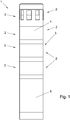
- a signaling device 1 for displaying operating conditions of a machine or a plant component is shown.
- the signaling device is designed as a signal tower with a plurality of signal modules 2, which, as will be explained in more detail below, are detachably connectable to each other.
- the individual signal modules 2 are arranged one above the other.
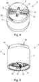
- the signal modules 2 'each have an outer housing 3, which with a cylindrical, partially transparent and each in another Color running lateral surface 4 and a lid 5 is formed (see. Fig. 4, 5 ).
- the signal modules 2 are arranged in a known manner on a base element 6, which is connected via (schematically drawn) electrical connection means with the (not shown) machine. Accordingly, the control of all signal modules 2 takes place via the common connection means of the base element 6.
- the optical signal modules 2 'each have at least one luminous element on the printed circuit boards 7.
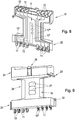
- a luminous element in particular at least one light-emitting diode (LED) is provided, wherein the in Fig. 8
- Signal element 8 shown comprises a total of six LEDs (three on each side of the printed circuit board element).
- the signal modules which in the embodiment shown as in Fig. 8 schematically apparent interconnects 10 are integrated into the circuit board elements 7.
- each circuit board element 7 has a leading to the next signal module 2 "0" conductor track 10 '. Furthermore, in each case at least one conductor track 10 "is provided, which establishes a connection from the contact element” 1 "to the right of the" 0 "track via the respective signal element 8 to the" 0 "track, as well as further conductive tracks 10 '". , By applying voltage to the "0" conductor track and one of the connection terminals 9 '"1" to "7", a corresponding signal module 2 can thus be activated.
- the signal modules 2 to the releasable connection bayonet connection elements 14 which are formed by bayonet projections 15 at an inwardly offset upper edge region of the lateral surface 4 of the outer housing 3 and corresponding bayonet openings 16 at the opposite lower edge region of the outer surface 3 of the outer housing ,
- the bayonet connection elements 14 of signal modules 2 arranged one above the other can be connected to one another in a known manner via a plug-in rotary connection.
- the bayonet projections 15 are guided on the lower signal module 2 in an axially extending input region 16a of the bayonet opening 16.
- the signal modules 2 are rotated against each other, wherein the bayonet projections 15 are displaced along horizontal securing portions 16 b of the bayonet openings 16.
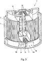
- the contact elements 11 of the one (upper) signal module 2 are arranged in the mated, untwisted state of the bayonet connection elements 14 at a distance from the corresponding contact points of the other signal module 2.
- the contact points 12, 13 superimposed signal modules 2 are brought into conductive contact.
- the signal line can be released or separated by the successive signal modules 2 via the bayonet connection.
- the lower-side pin elements 17 "are each connected to the contact elements 11, whereas the upper-side pin elements 17 'are free of such contact elements 11.
- the signal modules 2 each have an attachment element 18 for the associated printed circuit board element 7, wherein in a first embodiment, the associated circuit board element 7 is substantially completely received within the attachment element 18.
- the attachment element 18 has in a lower portion a protective element 25, with two rows of projections 19, one row being provided with longer projections 19 'and one row with shorter projections 19 ", the contact elements 11 each being between the projections serving as protection against contact 19 ', 19 "arranged.
- the longer projections 19 ' cover the contact elements 11 on the side on which no contact is made, substantially entirely.
- the shorter projections 19 '' release an end section of the contact elements 11 for contacting purposes.
- the contact elements 11 as well as the projections 19 ', 19' are accommodated in corresponding passage openings 20 at the top of the attachment element 18 of the adjacent signal module 2 when two signal modules 2 are brought together.
- the passage openings 20 of the attachment element 18 are arcuately curved.
- the pin-shaped projections 19 of the one (upper) signal module 2 are therefore moved in the arcuately curved passage openings 20 of the other (lower) signal module 2. Accordingly, the procedure is for the respective number of signal modules 2.
- the arrangement of the longer 19 'or shorter projections 19 is on the opposite radial sections of the attachment element 18 reversed.
- a contacting of adjacent circuit board elements 7 is reliably produced.
- the configuration of the shorter projections 19 assures that the contacting between the circuit board elements 7 when connecting the signal modules 2 is not hindered.
- the attachment element 18 has two half-shells 22, which are connected to one another via a latching connection 23.
- the attachment element 18 has a connection element 24, in which the passage openings 20 are provided, a protective element 25 with projections 19 ', 19 "and an optical element 26.
- the optical element 26 has a number of lenses 27, with which of the light beams emitted by the respectively associated LED of the signal element 8 is expediently distributed or directed
- the attachment element 18 itself is mounted in the outer housing 3 via a snap connection 29.
- FIG. 11 to 13 is another embodiment can be seen in which the attachment element 18 is significantly reduced compared to the first embodiment. That is, this attachment element 18 does not enclose the printed circuit board element 7 in the manner of a protective housing, but rather a printed circuit board element 7 is provided with a substantially constant width, which extends clearly above the attachment element 18, in particular in the region of the optical element 26 and the connecting element 24. Moreover, the attachment element 18, as described in connection with the first embodiment, a connecting element 24 with locking projections 24 'for attachment to the housing 3 and a separately or integrally formed with the housing 3 cover 5.
- the protective element 25 still encloses, in particular for the protection of contact elements 11, a lower end section of the printed circuit board element 7, the contact elements 11 between a row, as already described in detail in connection with the first exemplary embodiment short projections 19 "and long projections 19 'of the protective element 25 are received.
- the attachment element 18 is essentially composed of two half-shells 22, wherein the circuit board element 7 openings 31, 32 through which structurally simple connection between the two half-shells 22 of the attachment element 18 and the printed circuit board element 7 Connecting elements of the respective half-shell, in particular latching hooks 34 or connecting pins 35, for the purpose of producing a plug connection with the opposite half-shell of the attachment element 18 can be passed.
- the circuit board element 7 openings 31, 32 through which structurally simple connection between the two half-shells 22 of the attachment element 18 and the printed circuit board element 7 Connecting elements of the respective half-shell, in particular latching hooks 34 or connecting pins 35, for the purpose of producing a plug connection with the opposite half-shell of the attachment element 18 can be passed.
- latching hooks 34 or connecting pins 35 for the purpose of producing a plug connection with the opposite half-shell of the attachment element 18 can be passed.
Landscapes
- Engineering & Computer Science (AREA)
- General Engineering & Computer Science (AREA)
- Physics & Mathematics (AREA)
- General Physics & Mathematics (AREA)
- Structures For Mounting Electric Components On Printed Circuit Boards (AREA)
- Arrangement Of Elements, Cooling, Sealing, Or The Like Of Lighting Devices (AREA)
- Non-Portable Lighting Devices Or Systems Thereof (AREA)
- Fastening Of Light Sources Or Lamp Holders (AREA)
Claims (13)
- Dispositif de signalisation (1), en particulier pour une colonne de signalisation, servant à afficher des états de fonctionnement, avec au moins un module de signalisation (2), qui présente un élément de carte à circuits imprimés (7 ; 7') pour au moins un élément de signalisation (8) servant à émettre un signal, en particulier pour un élément d'éclairage servant à émettre une lumière de signalisation, dans lequel le module de signalisation (2) peut être relié de manière amovible à un autre module de signalisation (2) et les modules de signalisation (2) sont disposés les uns au-dessus des autres dans l'état relié, dans lequel le module de signalisation (2) présente un élément de liaison à baïonnette (14) destiné à être relié à un élément de liaison à baïonnette (14) de l'autre module de signalisation (2) et une ligne de liaison (9) s'étendant à travers le module de signalisation (2) est prévue afin de piloter un élément de carte à circuits imprimés (7'') de l'autre module de signalisation (2), caractérisé en ce que l'élément de carte à circuits imprimés (7') du module de signalisation (2) présente, afin de réaliser la ligne de liaison (9), une piste conductrice (10') associée à l'élément de signalisation (8) de l'autre module de signalisation (2), laquelle est reliée, dans l'état relié des modules de signalisation (2), par l'intermédiaire d'un élément de contact (11) à une piste conductrice (10 ; 10', 10'') au niveau de l'élément de carte à circuits imprimés (7'') de l'autre module de signalisation (2), dans lequel les éléments de carte à circuits imprimés (7 ; 7' ; 7'') sont disposés les uns par rapport aux autres, dans un état emboîté sans torsion des éléments de liaison à baïonnette (14), dans une position sans contact et, dans un état emboîté avec torsion des éléments de liaison à baïonnette (14), dans une position de contact.
- Dispositif de signalisation (1) selon la revendication 1, caractérisé en ce que l'élément de carte à circuits imprimés (7 ; 7', 7'') s'étend sensiblement sur toute la hauteur du module de signalisation (2), dans lequel l'élément de contact (11) est disposé, dans l'état relié des modules de signalisation (2), entre un emplacement de contact (12) situé côté supérieur d'un des éléments de carte à circuits imprimés (7') et un emplacement de contact (13) situé côté inférieur de l'autre élément de carte à circuits imprimés (7'').
- Dispositif de signalisation (1) selon la revendication 1 ou 2, caractérisé en ce qu'est prévu, en tant qu'élément de contact (11), un ressort de contact (11') pouvant être orienté de manière élastique, lequel relie, dans l'état relié des modules de signalisation (2), les éléments de carte à circuits imprimés (7 ; 7', 7'') de ces derniers entre eux.
- Dispositif de signalisation (1) selon l'une quelconque des revendications 1 à 3, caractérisé en ce que l'élément de carte à circuits imprimés (7 ; 7', 7'') présente des éléments de tourillon (17 ; 17', 17'') présentant des emplacements de contact (12, 13), faisant saillie du côté frontal situé côté supérieur et du côté frontal situé côté inférieur des éléments de carte à circuits imprimés (7 ; 7', 7''), dans lequel les éléments de tourillon (17 ; 17', 17'') situés côté inférieur ou côté supérieur sont reliés aux éléments de contact (11) et les éléments de tourillon (17 ; 17', 17'') situés côté supérieur et côté inférieur sont sans éléments de contact (11).
- Dispositif de signalisation (1) selon l'une quelconque des revendications 1 à 4, caractérisé en ce que le module de signalisation (2) présente un élément de rehausse (18) relié à l'élément de carte à circuits imprimés (7 ; 7', 7''), avec un élément de liaison (24), dans lequel l'élément de liaison est reçu, par l'intermédiaire d'une liaison amovible, de préférence une liaison à déclic (29), dans un boîtier (3) extérieur, de préférence avec une surface enveloppante cylindrique.
- Dispositif de signalisation (1) selon les revendications 1 à 5, caractérisé en ce qu'au moins un élément de protection (25) entourant au moins en partie les éléments de contact (11) est prévu afin de protéger les éléments de contact (11).
- Dispositif de signalisation (1) selon la revendication 6, caractérisé en ce que l'élément de protection (25) présente deux rangées de parties faisant saillie (19), entre lesquelles les éléments de contact (11) sont disposés, dans lequel une première rangée présente des parties faisant saillie (19'') comparativement courtes et une deuxième rangée présente des parties faisant saillie (19') comparativement longues.
- Dispositif de signalisation selon l'une quelconque des revendications 5 à 7, caractérisé en ce qu'un élément de couvercle et/ou de fond (5) de l'autre module de signalisation (2) ou l'élément de rehausse (18) d'un autre élément de carte à circuits imprimés (7 ; 7', 7'') présente au moins une ouverture de passage (20) incurvée de manière à présenter une forme d'arc.
- Dispositif de signalisation (1) selon l'une quelconque des revendications 1 à 8, caractérisé en ce qu'au moins un élément optique (26) est relié à l'élément de carte à circuits imprimés (7 ; 7', 7''), lequel présente au moins une lentille (27) optique, dans lequel de préférence le nombre des lentilles (27) correspond sensiblement à un nombre des diodes électroluminescentes prévues en tant qu'élément de signalisation (8).
- Dispositif de signalisation (1) selon l'une quelconque des revendications 1 à 9, caractérisé en ce qu'est prévu au moins un élément de rehausse (18) comprenant l'élément de liaison (24), l'élément de protection (25) et l'élément optique (26).
- Dispositif de signalisation (1) selon l'une quelconque des revendications 5 à 10, caractérisé en ce que l'élément de rehausse (18) présente deux demi-coques (22), qui sont reliées entre elles par l'intermédiaire d'une liaison amovible, de préférence d'une liaison à enclenchement (23).
- Dispositif de signalisation (1) selon l'une quelconque des revendications 1 à 11, caractérisé en ce qu'au moins un élément de carte à circuits imprimés (7 ; 7', 7'') présente plus de trois, de préférence au moins cinq, en particulier huit, pistes conductrices (10 ; 10', 10'', 10''') pour le pilotage d'un nombre correspondant de modules de signalisation (2).
- Dispositif de signalisation (1) selon l'une quelconque des revendications 1 à 12, caractérisé en ce que sont prévus au moins deux modules de signalisation (2) reliés les uns aux autres, disposés les uns au-dessus des autres dans l'état relié.
Priority Applications (6)
| Application Number | Priority Date | Filing Date | Title |
|---|---|---|---|
| ES15150795.1T ES2631809T3 (es) | 2015-01-12 | 2015-01-12 | Dispositivo de señalización |
| EP15150795.1A EP3043111B2 (fr) | 2015-01-12 | 2015-01-12 | Dispositif de signalisation |
| EP17164549.2A EP3205933A1 (fr) | 2015-01-12 | 2015-01-12 | Dispositif de signal |
| PL15150795T PL3043111T3 (pl) | 2015-01-12 | 2015-01-12 | Urządzenie sygnalizacyjne |
| US14/993,549 US10127779B2 (en) | 2015-01-12 | 2016-01-12 | Signalling device |
| US16/189,235 US10475304B2 (en) | 2015-01-12 | 2018-11-13 | Signalling device |
Applications Claiming Priority (1)
| Application Number | Priority Date | Filing Date | Title |
|---|---|---|---|
| EP15150795.1A EP3043111B2 (fr) | 2015-01-12 | 2015-01-12 | Dispositif de signalisation |
Related Child Applications (2)
| Application Number | Title | Priority Date | Filing Date |
|---|---|---|---|
| EP17164549.2A Division-Into EP3205933A1 (fr) | 2015-01-12 | 2015-01-12 | Dispositif de signal |
| EP17164549.2A Division EP3205933A1 (fr) | 2015-01-12 | 2015-01-12 | Dispositif de signal |
Publications (3)
| Publication Number | Publication Date |
|---|---|
| EP3043111A1 EP3043111A1 (fr) | 2016-07-13 |
| EP3043111B1 true EP3043111B1 (fr) | 2017-04-05 |
| EP3043111B2 EP3043111B2 (fr) | 2022-08-24 |
Family
ID=52347167
Family Applications (2)
| Application Number | Title | Priority Date | Filing Date |
|---|---|---|---|
| EP17164549.2A Withdrawn EP3205933A1 (fr) | 2015-01-12 | 2015-01-12 | Dispositif de signal |
| EP15150795.1A Active EP3043111B2 (fr) | 2015-01-12 | 2015-01-12 | Dispositif de signalisation |
Family Applications Before (1)
| Application Number | Title | Priority Date | Filing Date |
|---|---|---|---|
| EP17164549.2A Withdrawn EP3205933A1 (fr) | 2015-01-12 | 2015-01-12 | Dispositif de signal |
Country Status (4)
| Country | Link |
|---|---|
| US (2) | US10127779B2 (fr) |
| EP (2) | EP3205933A1 (fr) |
| ES (1) | ES2631809T3 (fr) |
| PL (1) | PL3043111T3 (fr) |
Cited By (1)
| Publication number | Priority date | Publication date | Assignee | Title |
|---|---|---|---|---|
| EP3587898A1 (fr) | 2018-06-26 | 2020-01-01 | AUER Signal GmbH | Boîtier |
Families Citing this family (12)
| Publication number | Priority date | Publication date | Assignee | Title |
|---|---|---|---|---|
| US10475299B2 (en) * | 2015-07-20 | 2019-11-12 | Banner Engineering Corporation | Modular indicator |
| DE102015120280A1 (de) * | 2015-11-24 | 2017-05-24 | Werma Holding Gmbh + Co. Kg | Signalgerät mit Leuchtmodul |
| USD839119S1 (en) * | 2015-12-24 | 2019-01-29 | Patlite Corporation | Signal warning and displaying lamp |
| CN106195803B (zh) * | 2016-09-07 | 2018-11-27 | 惠州雷士光电科技有限公司 | 一种用于导轨灯的插拔式接驳器及插拔组合导轨灯 |
| US10422821B2 (en) | 2017-04-17 | 2019-09-24 | Rockwell Automation Technologies, Inc. | System and method of identifying a module in a stack light |
| EP3419120A1 (fr) | 2017-06-19 | 2018-12-26 | AUER Signal GmbH | Dispositif de signal et connecteur |
| US11415281B2 (en) * | 2018-08-28 | 2022-08-16 | Mary Elle Fashions, Inc. | Flickering mineral light |
| GB2577757A (en) * | 2018-10-06 | 2020-04-08 | Eaton Intelligent Power Ltd | A stack light for indicating a status of an apparatus to be monitored |
| US11511915B2 (en) * | 2019-05-01 | 2022-11-29 | Brian Louis Lipshy | Child resistant container having an audio device |
| US11705679B2 (en) | 2020-12-18 | 2023-07-18 | Banner Engineering Corp. | In-line modular indicator assembly |
| JP7536109B2 (ja) * | 2021-06-29 | 2024-08-19 | シュナイダー・エレクトリック・アジア・ピーティーイー・リミテッド | タワーシグナルモジュール |
| EP4733866A1 (fr) | 2024-10-25 | 2026-04-29 | AUER Signal GmbH | Procédé de fonctionnement d'un appareil de signal, système de reproduction optique et/ou acoustique d'un état et produit programme informatique |
Citations (10)
| Publication number | Priority date | Publication date | Assignee | Title |
|---|---|---|---|---|
| DE19513983A1 (de) | 1994-04-15 | 1995-10-19 | Werma Signalgeraete Gmbh & Co | Signalsäule |
| DE29811425U1 (de) | 1998-06-29 | 1998-09-17 | Stocko Metallwarenfabriken Henkels & Sohn GmbH & Co, 42327 Wuppertal | Kontaktiereinheit für ein kartenförmiges Trägerelement elektronischer Baugruppen, insbesondere nach PCMCIA-Norm |
| DE19854666A1 (de) | 1998-11-26 | 2000-06-08 | Schneider Electric Gmbh | Signaleinrichtung |
| US6382811B1 (en) | 1999-05-28 | 2002-05-07 | Schneider Electric Industries Sa | Component of a signaling column |
| EP1467140A2 (fr) | 2003-04-09 | 2004-10-13 | WERMA Signaltechnik GmbH & Co.KG | Dispositif de signalisation |
| DE102006034164B4 (de) | 2006-05-09 | 2008-07-31 | Dehn + Söhne Gmbh + Co. Kg | Mehrpoliger Blitzstrom- und/oder Überspannungsableiter in Reihenklemmausführung |
| DE202013102472U1 (de) | 2013-06-10 | 2013-06-17 | Yellowtec GmbH | Warnleuchte, insbesondere Signalsäule sowie Leuchteinheit für eine solche |
| DE102011122530A1 (de) | 2011-12-29 | 2013-07-04 | Werma Holding Gmbh + Co. Kg | "Warnleuchtsäule mit einem elektrischen Kontakt zwischen zwei Wechselmodulen" |
| KR20140014423A (ko) | 2012-07-24 | 2014-02-06 | 주식회사 한영넉스 | 전자기기 구조체 |
| DE102012215611A1 (de) | 2012-09-04 | 2014-03-06 | Robert Bosch Gmbh | Kontaktsystem mit einer Leiterplatte und einem Stecker |
Family Cites Families (17)
| Publication number | Priority date | Publication date | Assignee | Title |
|---|---|---|---|---|
| US5814968A (en) * | 1995-06-26 | 1998-09-29 | Long Range Systems, Inc. | Battery charger and rechargeable electronic paging device assembly |
| US5963126A (en) * | 1997-02-27 | 1999-10-05 | Star Headlight And Lantern Co, Inc | Visual signaling device |
| DE10041202A1 (de) * | 2000-08-23 | 2002-03-21 | Lmg Signaltechnologie Kg | Signalsäule |
| DE10111594A1 (de) * | 2001-03-10 | 2002-09-19 | Karl Jautz Elektro Tech Spezia | Anzeigeleuchtensäule |
| US20030030567A1 (en) * | 2001-08-13 | 2003-02-13 | Hetzel William Hieby | Flexible functionality of stack light |
| DE10212895A1 (de) | 2002-03-22 | 2003-10-02 | Werma Signaltechnik Gmbh & Co | Signalsäule |
| JP4134748B2 (ja) * | 2003-02-21 | 2008-08-20 | 株式会社パトライト | 信号表示灯用ユニットおよび信号表示灯 |
| EP1575011B1 (fr) * | 2004-03-11 | 2012-05-09 | WERMA Holding GmbH + Co. KG | Dispositif de signalisation |
| FR2869975B1 (fr) | 2004-05-04 | 2006-06-16 | Schneider Electric Ind Sas | Colonne de signalisation verrouillable |
| EP1650489B1 (fr) * | 2004-10-22 | 2007-08-22 | WERMA Signaltechnik GmbH & Co.KG | Dispositif de signalisation, notamment colonne de signalisation |
| AU2008201153C1 (en) * | 2007-03-28 | 2011-01-06 | Aristocrat Technologies Australia Pty Limited | A Modular Visual Output Component |
| EP2209099B1 (fr) * | 2008-11-04 | 2011-10-26 | WERMA Holding GmbH + Co. KG | Dispositif de lampe de signalisation doté d'au moins deux lampes de signalisation |
| CN201425200Y (zh) | 2009-04-07 | 2010-03-17 | 山河电机厂股份有限公司 | 多层警示灯结构改良 |
| US9175827B2 (en) * | 2012-05-09 | 2015-11-03 | Lee Clore | Indicator light tower technology |
| US9307309B2 (en) | 2014-01-13 | 2016-04-05 | Rockwell Automation Technologies, Inc. | Stack light with in-line sound module |
| DE102014114111B4 (de) * | 2014-09-29 | 2025-09-25 | Werma Holding Gmbh + Co. Kg | Optisches Signalgerät |
| US9997031B2 (en) * | 2015-07-20 | 2018-06-12 | Banner Engineering Corporation | Modular indicator |
-
2015
- 2015-01-12 EP EP17164549.2A patent/EP3205933A1/fr not_active Withdrawn
- 2015-01-12 PL PL15150795T patent/PL3043111T3/pl unknown
- 2015-01-12 ES ES15150795.1T patent/ES2631809T3/es active Active
- 2015-01-12 EP EP15150795.1A patent/EP3043111B2/fr active Active
-
2016
- 2016-01-12 US US14/993,549 patent/US10127779B2/en active Active
-
2018
- 2018-11-13 US US16/189,235 patent/US10475304B2/en active Active
Patent Citations (10)
| Publication number | Priority date | Publication date | Assignee | Title |
|---|---|---|---|---|
| DE19513983A1 (de) | 1994-04-15 | 1995-10-19 | Werma Signalgeraete Gmbh & Co | Signalsäule |
| DE29811425U1 (de) | 1998-06-29 | 1998-09-17 | Stocko Metallwarenfabriken Henkels & Sohn GmbH & Co, 42327 Wuppertal | Kontaktiereinheit für ein kartenförmiges Trägerelement elektronischer Baugruppen, insbesondere nach PCMCIA-Norm |
| DE19854666A1 (de) | 1998-11-26 | 2000-06-08 | Schneider Electric Gmbh | Signaleinrichtung |
| US6382811B1 (en) | 1999-05-28 | 2002-05-07 | Schneider Electric Industries Sa | Component of a signaling column |
| EP1467140A2 (fr) | 2003-04-09 | 2004-10-13 | WERMA Signaltechnik GmbH & Co.KG | Dispositif de signalisation |
| DE102006034164B4 (de) | 2006-05-09 | 2008-07-31 | Dehn + Söhne Gmbh + Co. Kg | Mehrpoliger Blitzstrom- und/oder Überspannungsableiter in Reihenklemmausführung |
| DE102011122530A1 (de) | 2011-12-29 | 2013-07-04 | Werma Holding Gmbh + Co. Kg | "Warnleuchtsäule mit einem elektrischen Kontakt zwischen zwei Wechselmodulen" |
| KR20140014423A (ko) | 2012-07-24 | 2014-02-06 | 주식회사 한영넉스 | 전자기기 구조체 |
| DE102012215611A1 (de) | 2012-09-04 | 2014-03-06 | Robert Bosch Gmbh | Kontaktsystem mit einer Leiterplatte und einem Stecker |
| DE202013102472U1 (de) | 2013-06-10 | 2013-06-17 | Yellowtec GmbH | Warnleuchte, insbesondere Signalsäule sowie Leuchteinheit für eine solche |
Non-Patent Citations (3)
| Title |
|---|
| "Banner Engineering TL70 Modular Tower Light Provides Enhanced Customization and In-the-Field Modification Capabilities", BANNER ENGINEERING, 5 November 2014 (2014-11-05), XP055446826 |
| WERMA SIGNALTECHNIK: "WIN Control", NEW PRODUCTS 2014/2015, no. 00112014, XP055446795 |
| YELLOWTEC: "Litt signalleuchte", YELLOWTEC: RED DOT AWARD, 2017, XP055447461, Retrieved from the Internet <URL:http://archive.yellowtec.com/en/products-lp/litt/red-dot-award.html> |
Cited By (1)
| Publication number | Priority date | Publication date | Assignee | Title |
|---|---|---|---|---|
| EP3587898A1 (fr) | 2018-06-26 | 2020-01-01 | AUER Signal GmbH | Boîtier |
Also Published As
| Publication number | Publication date |
|---|---|
| EP3043111B2 (fr) | 2022-08-24 |
| US20190080571A1 (en) | 2019-03-14 |
| PL3043111T3 (pl) | 2017-09-29 |
| ES2631809T3 (es) | 2017-09-05 |
| US10127779B2 (en) | 2018-11-13 |
| US10475304B2 (en) | 2019-11-12 |
| EP3043111A1 (fr) | 2016-07-13 |
| US20160203686A1 (en) | 2016-07-14 |
| EP3205933A1 (fr) | 2017-08-16 |
Similar Documents
| Publication | Publication Date | Title |
|---|---|---|
| EP3043111B2 (fr) | Dispositif de signalisation | |
| EP3114403B1 (fr) | Luminaire comprenant des modules lumineux interchangeables | |
| EP3014169B1 (fr) | Luminaire destiné à être utilisé dans un système de rail d'éclairage ainsi que système de rail d'éclairage | |
| DE102013111578B4 (de) | Elektronikmodul | |
| EP1347233B1 (fr) | Colonne de signalisation | |
| DE3703423C2 (fr) | ||
| EP3114404B1 (fr) | Luminaire comprenant un élément support et un module lumineux fixé de manière libérable | |
| DE10111594A1 (de) | Anzeigeleuchtensäule | |
| DE19837553A1 (de) | Fahrzeugleuchte | |
| EP3114400B1 (fr) | Luminaire ou ensemble lumineux comprenant un élément support allongé et un module lumineux fixé de manière libérable | |
| EP3114734A1 (fr) | Borne de raccordement ou de connexion | |
| EP1107389A1 (fr) | Dispositif d'éclairage pour un véhicule | |
| DE102013002852B4 (de) | Verteilerbox | |
| DE202015009051U1 (de) | Signalvorrichtung | |
| EP2873913A1 (fr) | Lampe à DEL | |
| DE102013223412A1 (de) | Halterverbund und optoelektronische Anordnung | |
| WO2012135878A1 (fr) | Dispositif de fixation et de mise en contact d'une lampe et/ou d'un module lumineux, ainsi que luminaire | |
| EP3165821A1 (fr) | Élément de bande lumineuse allongé | |
| DE202015009420U1 (de) | Signalvorrichtung | |
| DE102018129122A1 (de) | Ladesteckverbinder mit einem Streuelement zum Abstrahlen und/oder Empfangen von Licht | |
| EP3805639B1 (fr) | Luminaire pourvu de contact enfichable, utilisation d'un tel luminaire et connecteur enfichable pour un tel luminaire | |
| DE102013022579B3 (de) | Elektronikmodul | |
| DE202013009191U1 (de) | Montieren einer Warnleuchtvorrichtung | |
| DE10058658A1 (de) | Dioden-Folien-Anordnung zur Beleuchtung | |
| DE102016211130A1 (de) | Herstellen einer elektrischen Verbindungsleitung mit mehreren Adern |
Legal Events
| Date | Code | Title | Description |
|---|---|---|---|
| REG | Reference to a national code |
Ref country code: DE Ref legal event code: R138 Ref document number: 202015009051 Country of ref document: DE Free format text: GERMAN DOCUMENT NUMBER IS 502015000791 |
|
| PUAI | Public reference made under article 153(3) epc to a published international application that has entered the european phase |
Free format text: ORIGINAL CODE: 0009012 |
|
| AK | Designated contracting states |
Kind code of ref document: A1 Designated state(s): AL AT BE BG CH CY CZ DE DK EE ES FI FR GB GR HR HU IE IS IT LI LT LU LV MC MK MT NL NO PL PT RO RS SE SI SK SM TR |
|
| AX | Request for extension of the european patent |
Extension state: BA ME |
|
| 17P | Request for examination filed |
Effective date: 20160727 |
|
| RBV | Designated contracting states (corrected) |
Designated state(s): AL AT BE BG CH CY CZ DE DK EE ES FI FR GB GR HR HU IE IS IT LI LT LU LV MC MK MT NL NO PL PT RO RS SE SI SK SM TR |
|
| GRAP | Despatch of communication of intention to grant a patent |
Free format text: ORIGINAL CODE: EPIDOSNIGR1 |
|
| STAA | Information on the status of an ep patent application or granted ep patent |
Free format text: STATUS: GRANT OF PATENT IS INTENDED |
|
| RIC1 | Information provided on ipc code assigned before grant |
Ipc: F21S 8/00 20060101ALI20161004BHEP Ipc: F21W 131/403 20060101ALN20161004BHEP Ipc: F21S 10/02 20060101ALI20161004BHEP Ipc: F21Y 115/10 20160101ALN20161004BHEP Ipc: F21V 23/06 20060101AFI20161004BHEP |
|
| INTG | Intention to grant announced |
Effective date: 20161107 |
|
| GRAS | Grant fee paid |
Free format text: ORIGINAL CODE: EPIDOSNIGR3 |
|
| GRAA | (expected) grant |
Free format text: ORIGINAL CODE: 0009210 |
|
| STAA | Information on the status of an ep patent application or granted ep patent |
Free format text: STATUS: THE PATENT HAS BEEN GRANTED |
|
| AK | Designated contracting states |
Kind code of ref document: B1 Designated state(s): AL AT BE BG CH CY CZ DE DK EE ES FI FR GB GR HR HU IE IS IT LI LT LU LV MC MK MT NL NO PL PT RO RS SE SI SK SM TR |
|
| REG | Reference to a national code |
Ref country code: GB Ref legal event code: FG4D Free format text: NOT ENGLISH |
|
| RIN1 | Information on inventor provided before grant (corrected) |
Inventor name: AUER, MICHAEL Inventor name: FEHRINGER, THOMAS |
|
| REG | Reference to a national code |
Ref country code: CH Ref legal event code: EP |
|
| REG | Reference to a national code |
Ref country code: AT Ref legal event code: REF Ref document number: 882171 Country of ref document: AT Kind code of ref document: T Effective date: 20170415 |
|
| REG | Reference to a national code |
Ref country code: IE Ref legal event code: FG4D Free format text: LANGUAGE OF EP DOCUMENT: GERMAN |
|
| REG | Reference to a national code |
Ref country code: DE Ref legal event code: R096 Ref document number: 502015000791 Country of ref document: DE |
|
| REG | Reference to a national code |
Ref country code: CH Ref legal event code: NV Representative=s name: ISLER AND PEDRAZZINI AG, CH |
|
| REG | Reference to a national code |
Ref country code: NL Ref legal event code: FP |
|
| REG | Reference to a national code |
Ref country code: SE Ref legal event code: TRGR |
|
| REG | Reference to a national code |
Ref country code: LT Ref legal event code: MG4D |
|
| REG | Reference to a national code |
Ref country code: ES Ref legal event code: FG2A Ref document number: 2631809 Country of ref document: ES Kind code of ref document: T3 Effective date: 20170905 |
|
| PG25 | Lapsed in a contracting state [announced via postgrant information from national office to epo] |
Ref country code: LT Free format text: LAPSE BECAUSE OF FAILURE TO SUBMIT A TRANSLATION OF THE DESCRIPTION OR TO PAY THE FEE WITHIN THE PRESCRIBED TIME-LIMIT Effective date: 20170405 Ref country code: HR Free format text: LAPSE BECAUSE OF FAILURE TO SUBMIT A TRANSLATION OF THE DESCRIPTION OR TO PAY THE FEE WITHIN THE PRESCRIBED TIME-LIMIT Effective date: 20170405 Ref country code: NO Free format text: LAPSE BECAUSE OF FAILURE TO SUBMIT A TRANSLATION OF THE DESCRIPTION OR TO PAY THE FEE WITHIN THE PRESCRIBED TIME-LIMIT Effective date: 20170705 Ref country code: GR Free format text: LAPSE BECAUSE OF FAILURE TO SUBMIT A TRANSLATION OF THE DESCRIPTION OR TO PAY THE FEE WITHIN THE PRESCRIBED TIME-LIMIT Effective date: 20170706 |
|
| REG | Reference to a national code |
Ref country code: FR Ref legal event code: PLFP Year of fee payment: 4 |
|
| PG25 | Lapsed in a contracting state [announced via postgrant information from national office to epo] |
Ref country code: BG Free format text: LAPSE BECAUSE OF FAILURE TO SUBMIT A TRANSLATION OF THE DESCRIPTION OR TO PAY THE FEE WITHIN THE PRESCRIBED TIME-LIMIT Effective date: 20170705 Ref country code: IS Free format text: LAPSE BECAUSE OF FAILURE TO SUBMIT A TRANSLATION OF THE DESCRIPTION OR TO PAY THE FEE WITHIN THE PRESCRIBED TIME-LIMIT Effective date: 20170805 Ref country code: RS Free format text: LAPSE BECAUSE OF FAILURE TO SUBMIT A TRANSLATION OF THE DESCRIPTION OR TO PAY THE FEE WITHIN THE PRESCRIBED TIME-LIMIT Effective date: 20170405 Ref country code: LV Free format text: LAPSE BECAUSE OF FAILURE TO SUBMIT A TRANSLATION OF THE DESCRIPTION OR TO PAY THE FEE WITHIN THE PRESCRIBED TIME-LIMIT Effective date: 20170405 |
|
| REG | Reference to a national code |
Ref country code: DE Ref legal event code: R026 Ref document number: 502015000791 Country of ref document: DE |
|
| PLBI | Opposition filed |
Free format text: ORIGINAL CODE: 0009260 |
|
| PLAX | Notice of opposition and request to file observation + time limit sent |
Free format text: ORIGINAL CODE: EPIDOSNOBS2 |
|
| PG25 | Lapsed in a contracting state [announced via postgrant information from national office to epo] |
Ref country code: RO Free format text: LAPSE BECAUSE OF FAILURE TO SUBMIT A TRANSLATION OF THE DESCRIPTION OR TO PAY THE FEE WITHIN THE PRESCRIBED TIME-LIMIT Effective date: 20170405 Ref country code: CZ Free format text: LAPSE BECAUSE OF FAILURE TO SUBMIT A TRANSLATION OF THE DESCRIPTION OR TO PAY THE FEE WITHIN THE PRESCRIBED TIME-LIMIT Effective date: 20170405 Ref country code: EE Free format text: LAPSE BECAUSE OF FAILURE TO SUBMIT A TRANSLATION OF THE DESCRIPTION OR TO PAY THE FEE WITHIN THE PRESCRIBED TIME-LIMIT Effective date: 20170405 Ref country code: DK Free format text: LAPSE BECAUSE OF FAILURE TO SUBMIT A TRANSLATION OF THE DESCRIPTION OR TO PAY THE FEE WITHIN THE PRESCRIBED TIME-LIMIT Effective date: 20170405 Ref country code: SK Free format text: LAPSE BECAUSE OF FAILURE TO SUBMIT A TRANSLATION OF THE DESCRIPTION OR TO PAY THE FEE WITHIN THE PRESCRIBED TIME-LIMIT Effective date: 20170405 |
|
| 26 | Opposition filed |
Opponent name: WERMA HOLDING GMBH + CO. KG Effective date: 20171222 |
|
| PG25 | Lapsed in a contracting state [announced via postgrant information from national office to epo] |
Ref country code: SM Free format text: LAPSE BECAUSE OF FAILURE TO SUBMIT A TRANSLATION OF THE DESCRIPTION OR TO PAY THE FEE WITHIN THE PRESCRIBED TIME-LIMIT Effective date: 20170405 |
|
| PLBB | Reply of patent proprietor to notice(s) of opposition received |
Free format text: ORIGINAL CODE: EPIDOSNOBS3 |
|
| PG25 | Lapsed in a contracting state [announced via postgrant information from national office to epo] |
Ref country code: MT Free format text: LAPSE BECAUSE OF FAILURE TO SUBMIT A TRANSLATION OF THE DESCRIPTION OR TO PAY THE FEE WITHIN THE PRESCRIBED TIME-LIMIT Effective date: 20170405 |
|
| PG25 | Lapsed in a contracting state [announced via postgrant information from national office to epo] |
Ref country code: LU Free format text: LAPSE BECAUSE OF NON-PAYMENT OF DUE FEES Effective date: 20180112 |
|
| REG | Reference to a national code |
Ref country code: IE Ref legal event code: MM4A |
|
| PG25 | Lapsed in a contracting state [announced via postgrant information from national office to epo] |
Ref country code: IE Free format text: LAPSE BECAUSE OF NON-PAYMENT OF DUE FEES Effective date: 20180112 |
|
| PGFP | Annual fee paid to national office [announced via postgrant information from national office to epo] |
Ref country code: PL Payment date: 20181109 Year of fee payment: 5 |
|
| PGFP | Annual fee paid to national office [announced via postgrant information from national office to epo] |
Ref country code: CH Payment date: 20190111 Year of fee payment: 5 Ref country code: ES Payment date: 20190201 Year of fee payment: 5 |
|
| PG25 | Lapsed in a contracting state [announced via postgrant information from national office to epo] |
Ref country code: MC Free format text: LAPSE BECAUSE OF FAILURE TO SUBMIT A TRANSLATION OF THE DESCRIPTION OR TO PAY THE FEE WITHIN THE PRESCRIBED TIME-LIMIT Effective date: 20170405 |
|
| APBM | Appeal reference recorded |
Free format text: ORIGINAL CODE: EPIDOSNREFNO |
|
| APBP | Date of receipt of notice of appeal recorded |
Free format text: ORIGINAL CODE: EPIDOSNNOA2O |
|
| APAH | Appeal reference modified |
Free format text: ORIGINAL CODE: EPIDOSCREFNO |
|
| APAW | Appeal reference deleted |
Free format text: ORIGINAL CODE: EPIDOSDREFNO |
|
| APBQ | Date of receipt of statement of grounds of appeal recorded |
Free format text: ORIGINAL CODE: EPIDOSNNOA3O |
|
| PLBP | Opposition withdrawn |
Free format text: ORIGINAL CODE: 0009264 |
|
| PG25 | Lapsed in a contracting state [announced via postgrant information from national office to epo] |
Ref country code: TR Free format text: LAPSE BECAUSE OF FAILURE TO SUBMIT A TRANSLATION OF THE DESCRIPTION OR TO PAY THE FEE WITHIN THE PRESCRIBED TIME-LIMIT Effective date: 20170405 |
|
| PG25 | Lapsed in a contracting state [announced via postgrant information from national office to epo] |
Ref country code: PT Free format text: LAPSE BECAUSE OF FAILURE TO SUBMIT A TRANSLATION OF THE DESCRIPTION OR TO PAY THE FEE WITHIN THE PRESCRIBED TIME-LIMIT Effective date: 20170405 |
|
| PG25 | Lapsed in a contracting state [announced via postgrant information from national office to epo] |
Ref country code: CY Free format text: LAPSE BECAUSE OF FAILURE TO SUBMIT A TRANSLATION OF THE DESCRIPTION OR TO PAY THE FEE WITHIN THE PRESCRIBED TIME-LIMIT Effective date: 20170405 Ref country code: MK Free format text: LAPSE BECAUSE OF NON-PAYMENT OF DUE FEES Effective date: 20170405 Ref country code: HU Free format text: LAPSE BECAUSE OF FAILURE TO SUBMIT A TRANSLATION OF THE DESCRIPTION OR TO PAY THE FEE WITHIN THE PRESCRIBED TIME-LIMIT; INVALID AB INITIO Effective date: 20150112 |
|
| PG25 | Lapsed in a contracting state [announced via postgrant information from national office to epo] |
Ref country code: AL Free format text: LAPSE BECAUSE OF FAILURE TO SUBMIT A TRANSLATION OF THE DESCRIPTION OR TO PAY THE FEE WITHIN THE PRESCRIBED TIME-LIMIT Effective date: 20170405 |
|
| REG | Reference to a national code |
Ref country code: FI Ref legal event code: MAE |
|
| REG | Reference to a national code |
Ref country code: CH Ref legal event code: PL |
|
| REG | Reference to a national code |
Ref country code: BE Ref legal event code: MM Effective date: 20200131 |
|
| PG25 | Lapsed in a contracting state [announced via postgrant information from national office to epo] |
Ref country code: FI Free format text: LAPSE BECAUSE OF NON-PAYMENT OF DUE FEES Effective date: 20200112 |
|
| PG25 | Lapsed in a contracting state [announced via postgrant information from national office to epo] |
Ref country code: BE Free format text: LAPSE BECAUSE OF NON-PAYMENT OF DUE FEES Effective date: 20200131 Ref country code: CH Free format text: LAPSE BECAUSE OF NON-PAYMENT OF DUE FEES Effective date: 20200131 Ref country code: SI Free format text: LAPSE BECAUSE OF NON-PAYMENT OF DUE FEES Effective date: 20180112 Ref country code: LI Free format text: LAPSE BECAUSE OF NON-PAYMENT OF DUE FEES Effective date: 20200131 |
|
| REG | Reference to a national code |
Ref country code: ES Ref legal event code: FD2A Effective date: 20210602 |
|
| PG25 | Lapsed in a contracting state [announced via postgrant information from national office to epo] |
Ref country code: ES Free format text: LAPSE BECAUSE OF NON-PAYMENT OF DUE FEES Effective date: 20200113 |
|
| APBU | Appeal procedure closed |
Free format text: ORIGINAL CODE: EPIDOSNNOA9O |
|
| PG25 | Lapsed in a contracting state [announced via postgrant information from national office to epo] |
Ref country code: PL Free format text: LAPSE BECAUSE OF NON-PAYMENT OF DUE FEES Effective date: 20200112 |
|
| PUAH | Patent maintained in amended form |
Free format text: ORIGINAL CODE: 0009272 |
|
| STAA | Information on the status of an ep patent application or granted ep patent |
Free format text: STATUS: PATENT MAINTAINED AS AMENDED |
|
| 27A | Patent maintained in amended form |
Effective date: 20220824 |
|
| AK | Designated contracting states |
Kind code of ref document: B2 Designated state(s): AL AT BE BG CH CY CZ DE DK EE ES FI FR GB GR HR HU IE IS IT LI LT LU LV MC MK MT NL NO PL PT RO RS SE SI SK SM TR |
|
| REG | Reference to a national code |
Ref country code: DE Ref legal event code: R102 Ref document number: 502015000791 Country of ref document: DE |
|
| REG | Reference to a national code |
Ref country code: SE Ref legal event code: RPEO |
|
| REG | Reference to a national code |
Ref country code: NL Ref legal event code: FP |
|
| PGFP | Annual fee paid to national office [announced via postgrant information from national office to epo] |
Ref country code: AT Payment date: 20230111 Year of fee payment: 9 |
|
| PGFP | Annual fee paid to national office [announced via postgrant information from national office to epo] |
Ref country code: SE Payment date: 20230123 Year of fee payment: 9 |
|
| P01 | Opt-out of the competence of the unified patent court (upc) registered |
Effective date: 20230517 |
|
| PGFP | Annual fee paid to national office [announced via postgrant information from national office to epo] |
Ref country code: NL Payment date: 20230127 Year of fee payment: 9 |
|
| REG | Reference to a national code |
Ref country code: SE Ref legal event code: EUG |
|
| REG | Reference to a national code |
Ref country code: NL Ref legal event code: MM Effective date: 20240201 |
|
| REG | Reference to a national code |
Ref country code: AT Ref legal event code: MM01 Ref document number: 882171 Country of ref document: AT Kind code of ref document: T Effective date: 20240112 |
|
| PG25 | Lapsed in a contracting state [announced via postgrant information from national office to epo] |
Ref country code: NL Free format text: LAPSE BECAUSE OF NON-PAYMENT OF DUE FEES Effective date: 20240201 |
|
| PG25 | Lapsed in a contracting state [announced via postgrant information from national office to epo] |
Ref country code: AT Free format text: LAPSE BECAUSE OF NON-PAYMENT OF DUE FEES Effective date: 20240112 |
|
| PG25 | Lapsed in a contracting state [announced via postgrant information from national office to epo] |
Ref country code: PL Free format text: THE PATENT HAS BEEN ANNULLED BY A DECISION OF A NATIONAL AUTHORITY Effective date: 20221124 |
|
| PG25 | Lapsed in a contracting state [announced via postgrant information from national office to epo] |
Ref country code: PL Free format text: THE PATENT HAS BEEN ANNULLED BY A DECISION OF A NATIONAL AUTHORITY Effective date: 20221124 Ref country code: NL Free format text: LAPSE BECAUSE OF NON-PAYMENT OF DUE FEES Effective date: 20240201 Ref country code: AT Free format text: LAPSE BECAUSE OF NON-PAYMENT OF DUE FEES Effective date: 20240112 |
|
| PGFP | Annual fee paid to national office [announced via postgrant information from national office to epo] |
Ref country code: FR Payment date: 20241220 Year of fee payment: 11 |
|
| PGFP | Annual fee paid to national office [announced via postgrant information from national office to epo] |
Ref country code: IT Payment date: 20250108 Year of fee payment: 11 Ref country code: GB Payment date: 20250120 Year of fee payment: 11 |
|
| PG25 | Lapsed in a contracting state [announced via postgrant information from national office to epo] |
Ref country code: SE Free format text: LAPSE BECAUSE OF NON-PAYMENT OF DUE FEES Effective date: 20240113 |
|
| PGFP | Annual fee paid to national office [announced via postgrant information from national office to epo] |
Ref country code: DE Payment date: 20260126 Year of fee payment: 12 |