EP3043111B2 - Signalvorrichtung - Google Patents
Signalvorrichtung Download PDFInfo
- Publication number
- EP3043111B2 EP3043111B2 EP15150795.1A EP15150795A EP3043111B2 EP 3043111 B2 EP3043111 B2 EP 3043111B2 EP 15150795 A EP15150795 A EP 15150795A EP 3043111 B2 EP3043111 B2 EP 3043111B2
- Authority
- EP
- European Patent Office
- Prior art keywords
- signalling
- circuit board
- elements
- contact
- module
- Prior art date
- Legal status (The legal status is an assumption and is not a legal conclusion. Google has not performed a legal analysis and makes no representation as to the accuracy of the status listed.)
- Active
Links
Images


Classifications
-
- G—PHYSICS
- G08—SIGNALLING
- G08B—SIGNALLING SYSTEMS, e.g. PERSONAL CALLING SYSTEMS; ORDER TELEGRAPHS; ALARM SYSTEMS
- G08B7/00—Signalling systems according to two or more of groups G08B3/00 - G08B6/00
- G08B7/06—Signalling systems according to two or more of groups G08B3/00 - G08B6/00 using electric transmission, e.g. involving audible and visible signalling through the use of sound and light sources
-
- F—MECHANICAL ENGINEERING; LIGHTING; HEATING; WEAPONS; BLASTING
- F21—LIGHTING
- F21S—NON-PORTABLE LIGHTING DEVICES; SYSTEMS THEREOF; VEHICLE LIGHTING DEVICES SPECIALLY ADAPTED FOR VEHICLE EXTERIORS
- F21S10/00—Lighting devices or systems producing a varying lighting effect
- F21S10/02—Lighting devices or systems producing a varying lighting effect changing colors
- F21S10/023—Lighting devices or systems producing a varying lighting effect changing colors by selectively switching fixed light sources
-
- F—MECHANICAL ENGINEERING; LIGHTING; HEATING; WEAPONS; BLASTING
- F21—LIGHTING
- F21S—NON-PORTABLE LIGHTING DEVICES; SYSTEMS THEREOF; VEHICLE LIGHTING DEVICES SPECIALLY ADAPTED FOR VEHICLE EXTERIORS
- F21S8/00—Lighting devices intended for fixed installation
-
- F—MECHANICAL ENGINEERING; LIGHTING; HEATING; WEAPONS; BLASTING
- F21—LIGHTING
- F21V—FUNCTIONAL FEATURES OR DETAILS OF LIGHTING DEVICES OR SYSTEMS THEREOF; STRUCTURAL COMBINATIONS OF LIGHTING DEVICES WITH OTHER ARTICLES, NOT OTHERWISE PROVIDED FOR
- F21V23/00—Arrangement of electric circuit elements in or on lighting devices
- F21V23/06—Arrangement of electric circuit elements in or on lighting devices the elements being coupling devices, e.g. connectors
-
- F—MECHANICAL ENGINEERING; LIGHTING; HEATING; WEAPONS; BLASTING
- F21—LIGHTING
- F21W—INDEXING SCHEME ASSOCIATED WITH SUBCLASSES F21K, F21L, F21S and F21V, RELATING TO USES OR APPLICATIONS OF LIGHTING DEVICES OR SYSTEMS
- F21W2131/00—Use or application of lighting devices or systems not provided for in codes F21W2102/00-F21W2121/00
- F21W2131/40—Lighting for industrial, commercial, recreational or military use
- F21W2131/403—Lighting for industrial, commercial, recreational or military use for machines
-
- F—MECHANICAL ENGINEERING; LIGHTING; HEATING; WEAPONS; BLASTING
- F21—LIGHTING
- F21Y—INDEXING SCHEME ASSOCIATED WITH SUBCLASSES F21K, F21L, F21S and F21V, RELATING TO THE FORM OR THE KIND OF THE LIGHT SOURCES OR OF THE COLOUR OF THE LIGHT EMITTED
- F21Y2115/00—Light-generating elements of semiconductor light sources
- F21Y2115/10—Light-emitting diodes [LED]
Definitions
- the invention relates to a signaling device, in particular for a signaling column, for displaying operating states, with at least one signaling module, which has a printed circuit board element for at least one signaling element for emitting a signal, in particular for a lighting element for emitting a signaling light, the signaling module being detachably connected to a further signal module can be connected and the signal modules are arranged one above the other in the connected state, the signal module having a bayonet connection element for connection to a bayonet connection element of the further signal module and a connecting line running through the signal module for controlling a printed circuit board element of the further signal module being provided.
- Such a signaling device with multiple signal modules is from EP 1 460 332 A2 known, wherein the signal modules each have a horizontally arranged circuit board element for at least one signal element ur delivery of a signal.
- the signal modules have wires running through the respective signal module as connecting lines for controlling a printed circuit board element of the further signal module. Plate elements are plugged onto the printed circuit boards to establish an electrical connection between the wires of adjacent signal modules in the connected state and to contact the printed circuit board element.
- the light column has a plurality of signaling elements which are essentially the same in terms of their design and are arranged one above the other and are connected to one another by means of a locking connection.
- the signaling elements consist of a cylindrical part for accommodating an optical or acoustic signal transmitter and electrical connecting lines, which are used for the individual power supply of the signaling elements.
- the electrical connecting lines are in the form of wires which each have an approximately U-shaped connecting bridge lying in an approximately tangentially aligned plane at one end and an angled connecting bridge at the other end.
- the connecting bridge of one signaling element interacts in a non-positive manner with the connecting web of the adjacent lighting element by means of a resilient wire connection.
- the electrical contact is made when the individual signaling elements are mechanically connected to one another via a bayonet connection.
- a particular disadvantage of this prior art is that connecting or supply lines interfere with the light image that may be emitted by the signaling element.
- the assembly is time-consuming and expensive.
- the arrangement of the connecting or feed lines within the signal elements requires a lot of space. As a result, the number of signal elements that can be arranged one above the other is limited for a given diameter of the cylindrical receiving part.
- a signaling column has already been proposed in the prior art, in which the signaling modules each have a printed circuit board.
- the signal modules are plugged into one another, with the printed circuit boards being connected to one another.
- this embodiment is disadvantageous in that the contacting between two printed circuit boards and the connection between two signal modules that are connected to one another must be carried out separately.
- the object of the present invention is to create a generic signaling device of the type mentioned at the outset, in which the individual signaling modules are contacted using structurally simple means that require little space, the signaling modules being disassembled at any point without the use of tools and can be reassembled.
- the printed circuit board element of the signal module has a conductor track assigned to the signal element of the further signal module to form the connecting line, which conductor track is connected in the connected state of the signal modules via a contact element to a conductor track on the printed circuit board element of the further signal module, the printed circuit board elements being in an assembled, non-twisted state of the Bayonet connection elements are arranged in a contact-free position and in a mated, twisted state of the bayonet connection elements in a contact position with respect to one another and run in one plane.
- connection or feed lines for supplying the signal elements across a number of signal modules are therefore advantageously integrated in the printed circuit board elements in the form of conductor tracks.
- Light-emitting elements for example light-emitting diodes, or sound signal elements can be provided as signaling elements.
- connecting or supply lines for example wire or platelet-shaped, running outside the printed circuit board elements.
- connection or feed lines were arranged at a distance from one another on the inside of the signal modules, running in the axial direction, which meant that the number of signal modules that could be arranged one above the other was actually limited in order to keep optical defects within an acceptable range.
- the mounting/assembly effort increased with the number of connection or feed lines to be attached.
- the printed circuit board element not only serves to control or supply the signaling element located thereon, but also to forward control or supply signals to the signaling elements of signaling modules located above it.
- the printed circuit board element has at least one conductor track, which is set up for forwarding electrical control or supply signals to a signal module located above it.
- each printed circuit board element has at least one conductor track connected to the signaling element of this signaling module, in order in particular to set the luminous state of the luminous element on the respective signaling module;
- the printed circuit board element can also have several signal elements supplied via different conductor tracks. The mounting/assembly effort is advantageously essentially independent of the number of conductor tracks.
- the circuit board elements are electrically conductively connected to one another via at least two contact elements.
- At least the lowest signal module preferably has a plurality of conductor tracks for forwarding control or supply signals to a plurality of signal modules above it, with a corresponding number of contact elements being provided between the signal modules.
- the signaling device can have a base element, preferably at the lower end, to which the control or supply signals for the individual signaling modules are supplied via connection means known per se in the prior art.
- the embodiment according to the invention brings with it the particular advantage that the number of signal modules that can be arranged one above the other and individually assembled or disassembled (with a given diameter) can be increased.
- the circuit board elements can be contacted more reliably when the signaling device is assembled.
- the configuration according to the invention is particularly stable.
- a further advantage of the invention lies in the fact that the signaling device can be installed more simply and therefore more cost-effectively.
- cost advantages can also be achieved through the parts-saving design.
- it is advantageous that the light emission from the signal modules to the environment is not impeded by feed lines.
- the signal module has a bayonet connection element for connection to a bayonet connection element of the further signal module, the printed circuit board elements being arranged in a contact-free position when the bayonet connection elements are plugged together and not twisted, and in a contact position with one another when the bayonet connection elements are plugged together and twisted.
- the signal modules have cooperating bayonet connection elements, which are formed by a bayonet projection on one signal module and a bayonet opening on the other signal module.
- the bayonet connection elements can be connected to one another by means of a plug-and-turn movement, the bayonet projection first being inserted through an axially extending entry area of the bayonet opening and then being twisted along a securing section of the bayonet opening running essentially at right angles thereto.
- the mechanical connection is coupled to the electrical connection between the printed circuit board elements via the bayonet connection elements.
- the contact elements of one signal module are arranged in a contact-free position with respect to the corresponding contact points of the other signal module when the bayonet connection elements are plugged together and not twisted.
- the contact elements of one signal module are brought into contact with the contact points of the other signal module.
- the signal line between the successive signal modules can be released or separated via the bayonet connection.
- the invention provides that the printed circuit board element extends essentially over the entire height of the signal module, with the contact element being located between a top-side contact point of one printed circuit board element when the signal modules are connected and an underside contact point of the other circuit board element is arranged.
- This embodiment is preferably provided for a signal module with a light-emitting element.
- the terms “up” and “down” refer to a substantially vertical operating position the signaling device in which the signaling modules are arranged one above the other.
- the printed circuit board element is preferably arranged in a substantially vertical position within the signal module, with the printed circuit board element extending over substantially the entire height of the associated signal module.
- the electrical control or supply signals through a signal module to an overlying signal module, at least two conductor tracks of this signal module are connected to associated conductor tracks of the overlying signal module via at least two contact elements. Accordingly, the signal is forwarded essentially over the entire height of the signaling device along the conductor tracks of the printed circuit board elements, with the successive signal modules being contacted by the contact elements.
- the invention provides that an elastically deflectable contact spring is provided as the contact element, which connects the circuit board elements of the signal modules to one another when they are in the connected state.
- Contact springs are therefore provided for contacting between the circuit board elements of signal modules arranged one above the other, which are applied to the corresponding contact points of the respective circuit board element when the mechanical connection is established between the signal modules.
- the circuit board element has contact points and pin elements protruding from the top and bottom end faces of the circuit board elements, with the bottom or top pin elements being connected to the contact elements are connected and the top and bottom pin elements are free of contact elements. Accordingly, the contact points of the printed circuit board element are connected to contact elements on one side, preferably on the underside, and are free of such contact elements on the other side, preferably on the upper side. When connecting the signal modules, the contact elements of one signal module always come into contact with contact points of the other signal module that are free of contact elements.
- the signal module has an attachment element with a connecting element that is connected to the printed circuit board element.
- the assembly of the signaling device can be carried out with little effort if the connecting element is accommodated in an outer housing, preferably with a cylindrical lateral surface, via a detachable connection, preferably a latching connection.
- the connecting element together with the printed circuit board element is snapped or latched in the outer housing.
- the outer housing preferably has a cylindrical lateral surface which is formed on one side with a cover or base part and on the other side with a holding opening for connection to the further signal module.
- the bayonet connection elements in the form of bayonet projections or bayonet openings are preferably provided at opposite ends of the lateral surface, in each case adjacent to the cover/bottom part or the retaining opening.
- the printed circuit board element can be arranged essentially completely within an attachment element that includes the connecting element.
- an attachment element in the form of a housing, the printed circuit board element and in particular also the contact elements are essentially completely protected from mechanical effects, in particular when the signal modules are connected.
- At least one protective element at least partially enclosing the contact elements is provided to protect the contact elements.
- the protective element preferably has a plurality of projections, preferably in the form of pins or pegs, which are arranged adjacent to the contact elements.
- two rows of such projections are provided, between which the contact elements are arranged, with a first row of comparatively short projections and a second row of comparatively long projections being provided.
- the contact points, in particular pin elements, of another printed circuit board element with which contact is to be made are advantageously arranged in such a way that they can be rotated over the short projections when the bayonet lock is closed without coming into contact with them.
- the long projections can advantageously be designed in such a way that they cover the contact elements essentially over the entire length on the side on which the contact elements are not intended to come into contact with a contact point, so that access to or damage to the contact elements is possible is prevented.
- a cover/base element of the further signal module or an attachment element of a further printed circuit board element has at least one arcuately curved through-opening.
- Contact elements and, if necessary, contact protection projections of a signal module can thus be inserted into through-openings of the other signal module in the plugged-in, untwisted state.
- the contact elements and the (contact protection) projections are then guided in the arcuate through-openings.
- the stop position is reached, which is preferably defined by the bayonet connection, the electrical contact between the printed circuit board elements is established via the contact elements.
- At least one optical element is connected to the circuit board element, which optical element has at least one optical lens, with preferably the number of lenses essentially corresponds to a number of the light-emitting diodes provided as a signaling element.
- a connecting element for an outer housing and a directed emission of the light beams generated in a structurally simple and cost-effective manner it is advantageous if at least one attachment element is provided comprising the connecting element, the protective element and the optical element.
- the signaling device can be assembled in a particularly simple manner if the attachment element has two half-shells which are connected to one another via a detachable connection, preferably a snap-in connection.
- the printed circuit board element is arranged between the half-shells of the attachment element, with the printed circuit board element being able to protrude in particular laterally beyond the assembled half-shells.
- At least one circuit board element has more than three, preferably at least five, in particular eight, conductor tracks for controlling a corresponding number of signaling modules.
- At least two signaling modules which are connected to one another and are arranged one above the other in the connected state are provided. At least two signal modules of the same type are preferably provided as light signal modules with light-emitting elements. In addition, a signal module with an audio signal element can be provided.
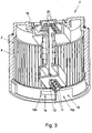
- a signaling device 1 for displaying operating states of a machine or a system component is shown.
- the signaling device is designed as a signaling column with a plurality of signaling modules 2 which, as will be explained in more detail below, can be detachably connected to one another. Im connected State are the individual signal modules 2 arranged one above the other.
- three optical signal modules 2' are provided for emitting light signals of different colors and one acoustic signal module 2'' (well known in the prior art) for emitting a sound signal.
- the signal modules 2' each have an outer housing 3, which is designed with a cylindrical, partially transparent lateral surface 4, each executed in a different color, and a cover 5 (cf. Figures 4, 5 ).
- the signal modules 2 are arranged in a known manner on a base element 6 which is connected to the machine (not shown) via electrical connection means (shown schematically). Accordingly, all signal modules 2 are controlled via the common connection means of the base element 6.
- the signal module 2 has a printed circuit board element 7 within the outer housing 3, on which in a known manner at least one (in 8 schematically drawn) signal element 8 is arranged to emit a signal.
- the optical signal modules 2 ′ each have at least one light-emitting element on the printed circuit boards 7 .
- at least one light-emitting diode (LED) is provided as the lighting element, with the in 8 signal element 8 shown comprises a total of six LEDs (three on each side of the circuit board element).
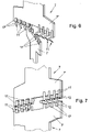
- Connecting lines running through the signal modules 2 are provided for controlling the printed circuit board elements 7, which in the embodiment shown are shown as 8 Schematically visible traces 10 are integrated into the printed circuit board elements 7.
- each printed circuit board element 7 has a "0” conductor track 10' leading to the next signal module 2. Furthermore, at least one conductor track 10'' is provided in each case, which establishes a connection from the contact element "1" to the right of the "0" conductor track via the respective signal element 8 to the "0" conductor track, as well as further conductor tracks 10''' that pass through. .
- a corresponding signal module 2 can thus be activated by applying voltage to the “0” conductor track and one of the connection terminals 9′ “1” to “7”.
- the conductor tracks 10', 10''' are electrically connected via contact elements 11 to the corresponding conductor tracks 10'' on the printed circuit board element 7 of the signal module 2 located above them. 1" is applied, the signal element 8 of the lowest signal module 2 lights up; if voltage is applied to the connection terminal 9'"0" and "2", the signal element 8 of the second signal module 2 (seen from below), etc. lights up 2 , 3
- the circuit board elements 7 extend essentially over the entire height or axial extent of the signal modules 2.
- the contact elements 11 are between a top contact point 12 of one (lower) circuit board element 7' and a bottom contact point 13 of the other (upper) printed circuit board element 7" (cf. 7 ).
- elastically deformable contact springs 11' are provided as contact elements 11, which in the connected state of the signal modules 2 have their printed circuit board elements 7; 7', 7" together (cf. 7 ).
- the signal modules 2 have bayonet connection elements 14 for their detachable connection, which are formed by bayonet projections 15 on an inwardly offset upper edge area of the lateral surface 4 of the outer housing 3 and corresponding bayonet openings 16 on the opposite, lower edge area of the lateral surface 4 of the outer housing 3 .
- the bayonet connection elements 14 of the signal modules 2 arranged one above the other can be connected to one another in a known manner via a plug-and-turn connection.
- the bayonet projections 15 on the lower signal module 2 are guided into an entry area 16a of the bayonet opening 16 running in the axial direction.
- the signal modules 2 are rotated in relation to one another, with the bayonet projections 15 being displaced along horizontal securing sections 16b of the bayonet openings 16 .
- the contact elements 11 of one (upper) signal module 2 are arranged at a distance from the corresponding contact points of the other signal module 2 when the bayonet connection elements 14 are plugged together and not twisted.
- the printed circuit board elements 7 have the contact points 12, 13 forming pin elements 17 which project upwards from the upper end face of the printed circuit board elements 7 or from the lower end face of the printed circuit board elements 7 downwards.
- the peg elements 17 ′′ on the underside are connected to the contact elements 11 , whereas the peg elements 17 ′ on the upper side are free of such contact elements 11 .
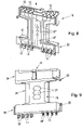
- the signal modules 2 each have an attachment element 18 for the associated printed circuit board element 7, with the associated printed circuit board element 7 being accommodated essentially completely within the attachment element 18 in a first exemplary embodiment.
- the attachment element 18 has a protective element 25 with two rows of projections 19, one row with longer projections 19' and a row with shorter projections 19" is provided.
- the contact elements 11 are each arranged between the projections 19', 19" serving as protection against accidental contact.
- the longer projections 19′ essentially completely cover the contact elements 11 on that side on which no contact is made.
- the shorter projections 19′′ leave an end section of the contact elements 11 free for the purpose of contacting.
- the contact elements 11 and the projections 19′, 19′′ are received in corresponding through-openings 20 on the upper side of the attachment element 18 of the adjacent signal module 2 when two signal modules 2 are brought together.
- the through openings 20 of the attachment element 18 are curved in an arc.
- the pin-shaped projections 19 of one (upper) signal module 2 are therefore moved in the arc-shaped passage openings 20 of the other (lower) signal module 2 .
- the procedure for the respective number of signal modules 2 is corresponding.
- the attachment element 18 has two half-shells 22 which are connected to one another via a snap-in connection 23 .
- the attachment element 18 has a connecting element 24 in which the through-openings 20 are provided, a protective element 25 with projections 19', 19" and an optical element 26.
- the optical element 26 has a number of lenses 27, with which of the light beams emitted by the respectively associated LED of the signaling element 8 is appropriately distributed or directed.
- attachment element 18 is significantly reduced compared to the first exemplary embodiment.
- this attachment element 18 does not enclose the printed circuit board element 7 in the manner of a protective housing, but rather a printed circuit board element 7 with a substantially constant width is provided, which extends significantly beyond the attachment element 18, particularly in the area of the optical element 26 and the connecting element 24.
- the attachment element 18 has, as described in connection with the first exemplary embodiment, a connecting element 24 with latching projections 24 ′ for the purpose of attachment to the housing 3 or a cover 5 formed separately or in one piece with the housing 3 .
- the through openings 20 are also formed in the cover 5 and not in the attachment element 18.
- the printed circuit board element 7, which is firmly connected to the attachment element 18, can thus be connected in a simple manner in the housing 3 by means of a snap connection, in particular to a central web 30 of the cover 5, via the latching lugs 24'.
- the protective element 25 still encloses a lower end section of the printed circuit board element 7, in particular to protect contact elements 11, whereby—as already described in detail in connection with the first exemplary embodiment—the contact elements 11 are located between a row short projections 19" and long projections 19' of the protective element 25 are accommodated.
- the attachment element 18 is also composed essentially of two half shells 22, with the printed circuit board element 7 having openings 31, 32 for the structurally simple connection between the two half shells 22 of the attachment element 18 and the printed circuit board element 7, through which Connecting elements of the respective half-shell, in particular latching hooks 34 or connecting pins 35, can be passed through in order to produce a plug-in connection with the opposite half-shell of the attachment element 18.
- Connecting elements of the respective half-shell, in particular latching hooks 34 or connecting pins 35 can be passed through in order to produce a plug-in connection with the opposite half-shell of the attachment element 18.
Landscapes
- Engineering & Computer Science (AREA)
- General Engineering & Computer Science (AREA)
- Physics & Mathematics (AREA)
- General Physics & Mathematics (AREA)
- Structures For Mounting Electric Components On Printed Circuit Boards (AREA)
- Arrangement Of Elements, Cooling, Sealing, Or The Like Of Lighting Devices (AREA)
- Non-Portable Lighting Devices Or Systems Thereof (AREA)
- Fastening Of Light Sources Or Lamp Holders (AREA)
Description
- Die Erfindung betrifft eine Signalvorrichtung, insbesondere für eine Signalsäule, zum Anzeigen von Betriebszuständen, mit zumindest einem Signalmodul, welches ein Leiterplattenelement für zumindest ein Signalelement zur Abgabe eines Signals, insbesondere für ein Leuchtelement zur Abgabe eines Signallichtes, aufweist, wobei das Signalmodul lösbar mit einem weiteren Signalmodul verbindbar ist und die Signalmodule im verbundenen Zustand übereinander angeordnet sind, wobei das Signalmodul ein Bajonettverbindungselement zur Verbindung mit einem Bajonettverbindungselement des weiteren Signalmoduls aufweist und eine durch das Signalmodul verlaufende Verbindungsleitung zur Ansteuerung eines Leiterplattenelements des weiteren Signalmoduls vorgesehen ist.
- Eine derartige Signalvorrichtung mit mehreren Signalmodulen ist aus der
EP 1 460 332 A2 bekannt, wobei die Signalmodule jeweils ein horizontal angeordnetes Leiterplattenelement für zumindest ein Signalelement ur Abgabe eines Signals aufweisen. Zudem weisen die Signalmodule durch das jeweilige Signalmodul verlaufende Drähte als Verbindungsleitungen zur Ansteuerung eines Leiterplattenelements des weiteren Signalmoduls auf. Zur elektrischen Verbindungherstellung zwischen den Drähten benachbarter Signalmodule im verbundenen Zustand und zur Kontaktierung des Leiterplattenelements sind Plattenelementen auf den Leiterplatten aufgesteckt. - Eine weitere Leuchtsäule zum Anzeigen von Betriebszuständen, beispielsweise von Fehlern an automatisch arbeitenden Maschinen, ist beispielsweise aus der
DE 195 13 983 A1 bekannt. Die Leuchtsäule weist mehrere, ihrer Bauart nach im Wesentlichen gleiche, übereinander angeordnete Signalelementen auf, die mittels einer Verschlussverbindung miteinander verbunden sind. Die Signalelemente bestehen aus einem Zylinderteil zur Aufnahme eines optischen bzw. akustischen Signalgebers und aus elektrischen Verbindungsleitungen, die zur individuellen Stromversorgung der Signalelemente dienen. Die elektrischen Verbindungsleitungen sind als Drähte ausgebildet, die jeweils an ihrem einen Ende eine etwa U-förmige, in einer etwa tangential ausgerichteten Ebene liegende Verbindungsbrücke und an ihrem anderen Ende einen abgewinkelten Verbindungssteg aufweisen. Die Verbindungsbrücke des einen Signalelements wirkt beim Zusammenbau zweier benachbarter Signalelemente mit dem Verbindungssteg des benachbarten Leuchtelements durch eine federnde Drahtverbindung kraftschlüssig zusammen. Dadurch wird die elektrische Kontaktierung vorgenommen, wenn die einzelnen Signalelemente über eine Bajonettverbindung mechanisch miteinander verbunden werden. - Auch aus der
EP 1 650 489 A2 ist eine Signalvorrichutung mit mehreren lösbar miteinander verbundenen Signalmodulen bekannt, die außerhalb des eingesetzten Elektronikträgers geführte Drähte zur Herstellung einer elektrischen Verbindung zwischen den Signalmodulen beim Zusammenfügen der Signalmodule aufweist. - Nachteilig an diesem Stand der Technik ist insbesondere, dass Verbindungs- bzw. Speiseleitungen das vom Signalelement gegebenenfalls abgegebene Lichtbild stören. Zudem ist die Assemblierung zeit- und kostenaufwändig. Darüber hinaus bringt die Anordnung der Verbindungs- bzw. Speiseleitungen innerhalb der Signalelemente einen hohen Platzbedarf mit sich. Dadurch ist die Anzahl der übereinander anordenbaren Signalelemente bei gegebenem Durchmesser des zylindrischen Aufnahmeteils limitiert.
- Darüber hinaus ist aus der
EP 1 347 233 A2 eine Signalsäule mit mehreren Segmenten unterschiedlicher Farbe bekannt geworden, bei welcher eine sich durch alle Segmente erstreckende Leiterplatte vorgesehen ist, die Leuchtdioden als Leuchtmittel trägt. Die Leuchtdioden sind jeweils einem Segment zugeordnet, wobei die Leuchtdioden verschiedener Segmente separat ansteuerbar sind. Bei dieser Ausführung ist jedoch nachteilig, dass die Variabilität der Leuchtsäule für verschiedene Anwendungen verloren geht. - Darüber hinaus wurde im Stand der Technik bereits eine Signalsäule vorgeschlagen, bei welchen die Signalmodule jeweils eine Leiterplatte aufweisen. Die Signalmodule werden bei dieser Ausführung ineinander gesteckt, wobei die Leiterplatten miteinander verbunden werden. Diese Ausführung ist jedoch dahingehend nachteilig, dass die Kontaktierung zwischen zwei Leiterplatten und die Verbindung zwischen zwei aneinander anschließenden Signalmodulen gesondert vorgenommen werden muss.
- Demnach besteht die Aufgabe der vorliegenden Erfindung darin, eine gattungsgemäße Signalvorrichtung der eingangs angeführten Art zu schaffen, bei welcher die Kontaktierung der einzelnen Signalmodule mit konstruktiv einfachen, geringen Platzbedarf benötigenden Mitteln bewerkstelligt wird, wobei die Signalmodule weiter ohne Verwendung von Werkzeugen an beliebiger Stelle auseinandergenommen und wieder zusammengesetzt werden können.
- Diese Aufgabe wird durch eine Signalvorrichtung mit den Merkmalen von Anspruch 1 gelöst. Bevorzugte Ausführungen sind in den abhängigen Ansprüchen angegeben.
- Erfindungsgemäß weist das Leiterplattenelement des Signalmoduls zur Ausbildung der Verbindungsleitung eine dem Signalelement des weiteren Signalmoduls zugeordnete Leiterbahn auf, welche im verbundenen Zustand der Signalmodule über ein Kontaktelement mit einer Leiterbahn am Leiterplattenelement des weiteren Signalmoduls verbunden ist, wobei die Leiterplattenelemente in einem zusammengesteckten, unverdrehten Zustand der Bajonettverbindungselemente in einer kontaktfreien Stellung und in einem zusammengesteckten, verdrehten Zustand der Bajonettverbindungselemente in einer Kontaktstellung zueinander angeordnet sind und in einer Ebene verlaufen.
- Vorteilhafterweise sind daher die Verbindungs- bzw. Speiseleitungen für die Versorgung der Signalelemente über mehrere Signalmodule hinweg in Form von Leiterbahnen in die Leiterplattenelemente integriert. Als Signalelemente können Leuchtelemente, beispielsweise Leuchtdioden, oder Tonsignalelemente vorgesehen sein. Dadurch kann auf außerhalb der Leiterplattenelemente verlaufende, beispielsweise draht- oder plättchenförmige Verbindungs- bzw. Speiseleitungen verzichtet werden. Solche Verbindungs- bzw. Speiseleitungen wurden beim Stand der Technik in Abstand zueinander an der Innenseite der Signalmodule, in axialer Richtung verlaufend angeordnet, wodurch - um optische Störstellen in einem akzeptablen Rahmen zu halten - die Anzahl übereinander anordenbarer Signalmodule faktisch begrenzt war. Zudem stieg der Montage-/Assemblieraufwand mit der Zahl der anzubringenden Verbindungs- bzw. Speiseleitungen. Bei der erfindungsgemäßen Signalvorrichtung dient das Leiterplattenelement nicht nur zur Ansteuerung bzw. Versorgung des darauf befindlichen Signalelements, sondern auch zur Weiterleitung von Steuer- bzw. Versorgungssignalen an die Signalelemente darüberliegender Signalmodule. Zu diesem Zweck weist das Leiterplattenelement zumindest eine Leiterbahn auf, welche zur Weiterleitung elektrischer Steuer- bzw. Versorgungssignale an ein darüberliegendes Signalmodul eingerichtet ist. Darüber hinaus weist jedes Leiterplattenelement zumindest eine mit dem Signalelement dieses Signalmoduls verbundene Leiterbahn auf, um insbesondere den Leuchtzustand des Leuchtelements am jeweiligen Signalmodul einzustellen; selbstverständlich kann das Leiterplattenelement aber auch mehrere, über unterschiedliche Leiterbahnen versorgte Signalelemente aufweisen. Der Montage-/Assemblieraufwand ist vorteilhafterweise von der Anzahl der Leiterbahnen im Wesentlichen unabhängig. Im mechanisch verbundenen Zustand der Signalmodule sind die Leiterplattenelemente über zumindest zwei Kontaktelemente elektrisch leitend miteinander verbunden. Bevorzugt weist zumindest das unterste Signalmodul mehrere Leiterbahnen zur Weiterleitung von Steuer- bzw. Versorgungssignalen an mehrere darüberliegende Signalmodule auf, wobei eine entsprechende Anzahl von Kontaktelementen zwischen den Signalmodulen vorgesehen ist. Beim Zusammenbau der Signalmodule wird somit zugleich die elektrische Kontaktierung der Leiterplattenelemente vorgenommen. Die Signalvorrichtung kann, bevorzugt am unteren Ende, ein Sockelelement aufweisen, welchem über im Stand der Technik an sich bekannte Anschlussmittel die Steuer- bzw. Versorgungssignale für die einzelnen Signalmodule zugeführt werden. Die erfindungsgemäße Ausführung bringt insbesondere den Vorteil mit sich, dass die Anzahl der übereinander anordenbaren, einzeln montierbaren bzw. demontierbaren Signalmodule (bei gegebenem Durchmesser) erhöht werden kann. Darüber hinaus kann die Kontaktierung der Leiterplattenelemente beim Zusammenbau der Signalvorrichtung zuverlässiger vorgenommen werden. Weiters ist die erfindungsgemäße Ausgestaltung besonders stabil. Ein weiterer Vorteil der Erfindung liegt darin, dass die Montage der Signalvorrichtung einfacher und daher kostengünstiger durchgeführt werden kann. Zudem können Kostenvorteile auch durch die teilesparende Ausführung erzielt werden. Schließlich ist von Vorteil, dass die Lichtabgabe der Signalmodule an die Umgebung nicht durch Speiseleitungen behindert wird.
- Darüber hinaus weist das Signalmodul ein Bajonettverbindungselement zur Verbindung mit einem Bajonettverbindungselement des weiteren Signalmoduls auf, wobei die Leiterplattenelemente in einem zusammengesteckten, unverdrehten Zustand der Bajonettverbindungselemente in einer kontaktfreien Stellung und in einem zusammengesteckten, verdrehten Zustand der Bajonettverbindungselemente in einer Kontaktstellung zueinander angeordnet sind. Im Stand der Technik ist es an sich bekannt, die Signalmodule über Bajonettverbindungen lösbar miteinander zu verbinden. Zu diesem Zweck weisen die Signalmodule zusammenwirkende Bajonettverbindungselemente auf, welche durch einen Bajonettvorsprung auf dem einen Signalmodul und eine Bajonettöffnung auf dem anderen Signalmodul gebildet sind. Die Bajonettverbindungselemente sind über eine Steck-Dreh-Bewegung miteinander verbindbar, wobei der Bajonettvorsprung zunächst durch einen in axialer Richtung verlaufenden Eingangsbereich der Bajonettöffnung gesteckt und danach entlang eines dazu im Wesentlichen rechtwinkelig verlaufenden Sicherungsabschnitts der Bajonettöffnung verdreht wird. Bei der vorliegenden Ausführung ist die mechanische Verbindung über die Bajonettverbindungselemente mit der elektrischen Verbindung zwischen den Leiterplattenelementen gekoppelt. Zu diesem Zweck sind die Kontaktelemente des einen Signalmoduls in dem zusammengesteckten, unverdrehten Zustand der Bajonettverbindungselemente in einer kontaktfreien Stellung zu den entsprechenden Kontaktstellen des anderen Signalmoduls angeordnet. Durch Anordnung der Bajonettverbindungselemente in der zusammengesteckten, verdrehten Stellung werden die Kontaktelemente des einen Signalmoduls in Kontakt mit den Kontaktstellen des anderen Signalmoduls gebracht. Somit kann die Signalleitung zwischen den aufeinanderfolgenden Signalmodulen über die Bajonettverbindung freigegeben bzw. getrennt werden.
- Um ein bestimmtes Signalmodul der Signalsäule mit einer Steuer- bzw. Versorgungsspannung beaufschlagen zu können, ist erfindungsgemäß vorgesehen, dass sich das Leiterplattenelement im Wesentlichen über die gesamte Höhe des Signalmoduls erstreckt, wobei das Kontaktelement im verbundenen Zustand der Signalmodule zwischen einer oberseitigen Kontaktstelle des einen Leiterplattenelements und einer unterseitigen Kontaktstelle des anderen Leiterplattenelements angeordnet ist. Diese Ausführung ist bevorzugt bei einem Signalmodul mit einem Leuchtelement vorgesehen. Für die Zwecke dieser Offenbarung beziehen sich die Bezeichnungen "oben" und "unten" auf eine im Wesentlichen vertikale Betriebsstellung der Signalvorrichtung, bei welcher die Signalmodule übereinander angeordnet sind. In dieser vertikalen bzw. stehenden Betriebsstellung der Signalvorrichtung ist das Leiterplattenelement bevorzugt in einer im Wesentlichen vertikalen Stellung innerhalb des Signalmoduls angeordnet, wobei sich das Leiterplattenelement jeweils über im Wesentlichen die gesamte Höhe des zugehörigen Signalmoduls erstreckt. Um die elektrische Steuer- bzw. Versorgungssignale durch ein Signalmodul hindurch zu einem darüberliegenden Signalmodul weiterzuleiten, ist zumindest zwei Leiterbahnen dieses Signalmoduls über zumindest zwei Kontaktelemente mit zugehörigen Leiterbahnen des darüberliegenden Signalmoduls verbunden. Demnach erfolgt die Signalweiterleitung im Wesentlichen über die gesamte Höhe der Signalvorrichtung entlang der Leiterbahnen der Leiterplattenelemente, wobei die aufeinanderfolgenden Signalmodule durch die Kontaktelemente kontaktiert werden.
- Um den elektrischen Kontakt zwischen den Signalmodulen zuverlässig herzustellen oder trennen zu können, ist erfindungsgemäß vorgesehen, dass als Kontaktelement eine elastisch auslenkbare Kontaktfeder vorgesehen ist, welche im verbundenen Zustand der Signalmodule deren Leiterplattenelemente miteinander verbindet. Zur Kontaktierung zwischen den Leiterplattenelementen übereinander angeordneter Signalmodule sind daher Kontaktfedern vorgesehen, welche beim Herstellen der mechanischen Verbindung zwischen den Signalmodulen an den entsprechenden Kontaktstellen des jeweiligen Leiterplattenelements angelegt werden. Durch Abnehmen eines Signalmoduls von der Signalvorrichtung wird zugleich die elektrische Verbindung über die Kontaktfedern getrennt. Zur zuverlässigen Durchkontaktierung der Signalmodule liegen die Kontaktfedern im verbundenen Zustand der Signalmodule mit einem Anpressdruck an den entsprechenden Kontaktstellen an.
- Um die Kontaktierung zwischen den Signalmodulen auf konstruktiv einfache, zuverlässige Weise zu bewerkstelligen, ist es von Vorteil, wenn das Leiterplattenelement Kontaktstellen aufweisende, von der ober- und der unterseitigen Stirnseite der Leiterplattenelemente abstehende Zapfenelemente aufweist, wobei die unter- oder oberseitigen Zapfenelemente mit den Kontaktelementen verbunden sind und die ober- bzw. unterseitigen Zapfenelemente frei von Kontaktelementen sind. Demnach sind die Kontaktstellen des Leiterplattenelements auf der einen Seite, vorzugsweise auf der Unterseite, mit Kontaktelementen verbunden und auf der anderen Seite, vorzugsweise auf der Oberseite, frei von solchen Kontaktelementen. Beim Verbinden der Signalmodule treten so stets die Kontaktelemente des einen Signalmoduls mit von Kontaktelementen freien Kontaktstellen des anderen Signalmoduls in Kontakt.
- Zur stabilen Halterung der Leiterplattenelemente innerhalb der Signalmodule ist es vorteilhaft, wenn das Signalmodul ein mit dem Leiterplattenelement verbundenes Aufsatzelement mit einem Verbindungselement aufweist. Die Montage der Signalvorrichtung kann mit geringem Aufwand vorgenommen werden, wenn das Verbindungselement über eine lösbare Verbindung, vorzugsweise eine Rastverbindung, in einem äußeren Gehäuse, vorzugsweise mit einer zylindrischen Mantelfläche, aufgenommen ist. Bei dieser Ausführung wird daher das Verbindungselement samt dem Leiterplattenelement in dem äußeren Gehäuse verschnappt bzw. verrastet. Das äußere Gehäuse weist bevorzugt eine zylindrische Mantelfläche auf, welche auf der einen Seite mit einem Deckel- bzw. Bodenteil und auf der anderen Seite mit einer Halteöffnung zum Verbinden mit dem weiteren Signalmodul ausgebildet ist. Bevorzugt sind an gegenüberliegenden Enden der Mantelfläche, jeweils benachbart des Deckel-/Bodenteils bzw. der Halteöffnung, die Bajonettverbindungselemente in Form der Bajonettvorsprünge bzw. der Bajonettöffnungen vorgesehen.
- Bei einer Ausführung kann das Leiterplattenelement im Wesentlichen vollständig innerhalb eines das Verbindungselement umfassenden Aufsatzelements angeordnet sein. Mit einem derartigen Aufsatzelement in der Art eines Gehäuses wird das Leiterplattenelement und insbesondere auch die Kontaktelemente im Wesentlichen vollständig vor mechanischen Einwirkungen, insbesondere beim Verbinden der Signalmodule, geschützt.
- Um die elektrische und mechanische Verbindung übereinander angeordneter Signalmodule ohne die Gefahr von Beschädigungen zuverlässig herstellen und trennen zu können, ist es günstig, wenn zum Schutz der Kontaktelemente zumindest ein die Kontaktelemente zumindest teilweise umschließendes Schutzelement vorgesehen ist. Bevorzugt weist das Schutzelement mehrere, vorzugsweise stift- oder zapfenförmige Vorsprünge auf, welche benachbart der Kontaktelemente angeordnet sind.
- Insbesondere sind hierbei zwei Reihen derartiger Vorsprünge vorgesehen, zwischen welchen die Kontaktelemente angeordnet sind, wobei eine erste Reihe vergleichsweise kurze Vorsprünge und eine zweite Reihe vergleichsweise lange Vorsprünge vorgesehen sind. Die Kontaktstellen, insbesondere Zapfenelemente, eines weiteren Leiterplattenelements, mit welchen eine Kontaktierung herzustellen ist, sind beim Zusammenführen der Signalmodule vorteilhafterweise derart angeordnet, dass sie beim Schließen des Bajonettverschlusses über den kurzen Vorsprünge hinweg gedreht werden können, ohne mit diesen in Berührung zu kommen.
- Die langen Vorsprünge hingegen können vorteilhafterweise derart ausgebildet sein, dass sie an jener Seite, an welcher die Kontaktelemente nicht zur Berührung mit einer Kontaktstelle vorgesehen sind, die Kontaktelemente im Wesentlichen über die gesamte Länge bedecken, so dass ein Zugriff bzw. eine Beschädigung der Kontaktelemente möglichst verhindert wird.
- Um eine Kontaktherstellung über die Drehbewegung bei Schließen der Bajonettverbindung ohne freiliegende, einem Zugriff ausgesetzte Kontaktstellen zu ermöglichen, ist es günstig, wenn ein Deckel-/Bodenelement des weiteren Signalmoduls oder ein Aufsatzelement eines weiteren Leiterplattenelements zumindest eine bogenförmig gekrümmte Durchgangsöffnung aufweist. Kontaktelemente sowie ggf. Berührungsschutz-Vorsprünge eines Singalmoduls können somit im zusammengesteckten, unverdrehten Zustand in Durchgangsöffnungen des anderen Signalmoduls eingeführt werden. Beim Verdrehen der Signalmodule gegeneinander werden die Kontaktelemente ebenso wie die (Berührungsschutz-) Vorsprünge sodann in den bogenförmigen Durchgangsöffnungen geführt. Mit Erreichen der Anschlagstellung, welche vorzugsweise über die Bajonettverbindung definiert ist, ist der elektrische Kontakt zwischen den Leiterplattenelementen über die Kontaktelemente hergestellt.
- Um den optischen Effekt des vom Signalelement abgesendeten Lichtsignals zu verbessern, d.h. insbesondere eine gerichtete Abstrahlung der erzeugten Lichtstrahlen zu erzielen, ist es günstig, wenn mit dem Leiterplattenelement zumindest ein Optikelement verbunden ist, das zumindest eine optische Linse aufweist, wobei vorzugsweise die Anzahl der Linsen im Wesentlichen einer Anzahl der als Signalelement vorgesehenen Leuchtdioden entspricht.
- Um auf konstruktiv einfache und kostengünstige Weise einen Schutz der Kontaktelemente, ein Verbindungselement für ein äußeres Gehäuse und eine gerichtete Abgabe der erzeugten Lichtstrahlen zu bewirken, ist es vorteilhaft, wenn zumindest ein Aufsatzelement umfassend das Verbindungselement, das Schutzelement und das Optikelement vorgesehen ist. Durch die Zusammenfassung der drei vorstehend genannten unterschiedlichen Funktionen in einem einzigen Aufsatzelement kann sowohl die Teilezahl als auch der Assemblierungsaufwand gering gehalten werden.
- Der Zusammenbau der Signalvorrichtung kann besonders einfach gestaltet werden, wenn das Aufsatzelement zwei Halbschalen aufweist, welche über eine lösbare Verbindung, vorzugsweise eine Rastverbindung, miteinander verbunden sind. Im montierten Zustand ist daher das Leiterplattenelement zwischen den Halbschalen des Aufsatzelements angeordnet, wobei das Leiterplattenelement jedoch insbesondere seitlich über die zusammengesetzten Halbschalen hinausragen kann.
- Zur Erzielung einer vielseitig verwendbaren Signalsäule ist es günstig, wenn zumindest ein Leiterplattenelement mehr als drei, vorzugsweise zumindest fünf, insbesondere acht, Leiterbahnen für die Ansteuerung einer entsprechenden Anzahl von Signalmodulen aufweist.
- Zur Erzielung einer Signalsäule ist es günstig, wenn zumindest zwei miteinander verbundene, im verbundenen Zustand übereinander angeordnete Signalmodule vorgesehen sind. Bevorzugt sind zumindest zwei gleichartige Signalmodule als Lichtsignalmodule mit Leuchtelementen vorgesehen. Zudem kann ein Signalmodul mit einem Tonsignalelement vorgesehen sein.
- Die Erfindung wird nachstehend anhand von bevorzugten Ausführungsbeispielen, auf die sie jedoch nicht beschränkt sein soll, noch weiter erläutert. In der Zeichnung zeigen:
-
Fig. 1 eine Ansicht einer erfindungsgemäßen Signalsäule, welche mehrere lösbar miteinander verbundene Signalmodule zur optischen und akustischen Anzeige von Betriebszuständen einer Maschine aufweist; -
Fig. 2 eine teilweise geschnittene, schaubildliche Ansicht eines Signalmoduls der Signalsäule gemäßFig. 1 , wobei das Signalmodul ein Leiterplattenelement mit einem LED-Leuchtelement aufweist; -
Fig. 3 eine weitere teilweise geschnittene, schaubildliche Ansicht des Signalmoduls gemäßFig. 1 ,2 ; -
Fig. 4, 5 weitere schaubildliche Ansichten des Signalmoduls gemäßFig. 1 bis 3 ; -
Fig. 6 und Fig. 7 schematische Ansichten der Leiterplattenelemente übereinander angeordneter Signalmodule, deren Leiterbahnen über Kontaktfedern durch Verdrehung zwischen der inFig. 6 dargestellten Ruhestellung und der inFig. 7 dargestellten Kontaktstellung miteinander verbindbar sind; -
Fig. 8 eine schaubildliche Ansicht einer Halbschale eines Aufsatzelements mit eingesetztem Leiterplattenelement; und -
Fig. 9 eine weitere schaubildliche Ansicht der Halbschale des Aufsatzelements für das Leiterplattenelement; -
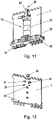
Fig. 10 eine schematische Ansicht von vier übereinander angeordneten Leiterplattenelementen; -
Fig. 11 eine schaubildliche Ansicht eines zweiten Ausführungsbeispiels eines erfindungsgemäßen Leiterplattenelements mit einem Aufsatzelement; -
Fig. 12 eine schaubildliche Ansicht des Ausführungsbeispiels gemäßFig. 11 mit einer abgenommenen Halbschale des Aufsatzelements; und -
Fig. 13 eine geschnittene schaubildliche Ansicht eines zweiten Ausführungsbeispiels eines erfindungsgemäßen Signalmoduls. - In
Fig. 1 ist eine Signalvorrichtung 1 zum Anzeigen von Betriebszuständen einer Maschine bzw. einer Anlagenkomponente gezeigt. Die Signalvorrichtung ist als Signalsäule mit mehreren Signalmodulen 2 ausgebildet, welche, wie nachstehend noch näher erläutert wird, lösbar miteinander verbindbar sind. Im verbundenen Zustand sind die einzelnen Signalmodule 2 übereinander angeordnet. In der gezeigten Ausführung sind drei optische Signalmodule 2' zur Abgabe verschiedenfarbiger Lichtsignale und ein (im Stand der Technik hinreichend bekanntes) akustisches Signalmodul 2'' zur Abgabe eines Tonsignals vorgesehen. Die Signalmodule 2' weisen jeweils ein äußeres Gehäuse 3 auf, welches mit einer zylindrischen, teilweise durchsichtigen und jeweils in einer anderen Farbe ausgeführten Mantelfläche 4 und einem Deckel 5 ausgebildet ist (vgl.Fig. 4, 5 ). Die Signalmodule 2 sind in bekannter Weise auf einem Sockelelement 6 angeordnet, welches über (schematisch eingezeichnete) elektrische Anschlussmittel mit der (nicht gezeigten) Maschine verbunden ist. Demnach erfolgt die Ansteuerung sämtlicher Signalmodule 2 über die gemeinsamen Anschlussmittel des Sockelelementes 6. - Wie aus
Fig. 2 ,3 ersichtlich, weist das Signalmodul 2 innerhalb des äußeren Gehäuses 3 ein Leiterplattenelement 7 auf, an welchem in bekannter Weise zumindest ein (inFig. 8 schematisch eingezeichnetes) Signalelement 8 zur Abgabe eines Signals angeordnet ist. Die optischen Signalmodule 2' weisen auf den Leiterplatten 7 jeweils zumindest ein Leuchtelement auf. Als Leuchtelement ist insbesondere zumindest eine Leuchtdiode (LED) vorgesehen, wobei das inFig. 8 gezeigte Signalelement 8 insgesamt sechs LEDs (drei auf jeder Seite des Leiterplattenelements) umfasst. Zur Ansteuerung der Leiterplattenelemente 7 sind durch die Signalmodule 2 verlaufende Verbindungsleitungen vorgesehen, welche in der gezeigten Ausführung als inFig. 8 schematisch ersichtliche Leiterbahnen 10 in die Leiterplattenelemente 7 integriert sind. - In
Fig. 10 sind vier übereinander angeordnete Leiterplattenelemente 7 gezeigt sowie schematisch im Sockelelement 6 integriert eine Basis 9 mit Anschlussklemmen 9' ("0" bis "7"). Demnach weist jedes Leiterplattenelement 7 einen zum nächsten Signalmodul 2 führende "0"-Leiterbahn 10' auf. Weiters ist jeweils zumindest eine Leiterbahn 10'' vorgesehen, welche eine Verbindung von dem Kontaktelement "1" rechts von der "0"-Leiterbahn über das jeweilige Signalelement 8 zu der "0"-Leiterbahn herstellt, sowie weitere durchführende Leiterbahnen 10'''. Über Anlage von Spannung an der "0"-Leiterbahn und einer der Anschlussklemmen 9' "1" bis "7" kann somit ein entsprechendes Signalmodul 2 aktiviert werden. Im mechanisch verbundenen Zustand der Signalmodule 2 sind die Leiterbahnen 10', 10"' über Kontaktelemente 11 mit den entsprechenden Leiterbahnen 10'' am Leiterplattenelement 7 des darüber liegenden Signalmoduls 2 elektrisch verbunden. Sofern daher Spannung an die Anschlussklemme 9' "0" und "1" angelegt wird, leuchtet das Signalelement 8 des untersten Signalmoduls 2; sofern Spannung an die Anschlussklemme 9' "0" und "2" angelegt wird, leuchtet das Signalelement 8 des (von unten gesehen) zweiten Signalmoduls 2, etc.. Wie ausFig. 2 ,3 weiters ersichtlich, erstrecken sich die Leiterplattenelemente 7 im Wesentlichen über die gesamte Höhe bzw. axiale Erstreckung der Signalmodule 2. Im verbundenen Zustand der Signalmodule 2 sind die Kontaktelemente 11 zwischen einer oberseitigen Kontaktstelle 12 des einen (unteren) Leiterplattenelements 7' und einer unterseitigen Kontaktstelle 13 des anderen (oberen) Leiterplattenelements 7" angeordnet (vgl.Fig. 7 ). Als Kontaktelemente 11 sind in der gezeigten Ausführung elastisch verformbare Kontaktfedern 11' vorgesehen, welche im verbundenen Zustand der Signalmodule 2 deren Leiterplattenelemente 7; 7', 7" miteinander verbinden (vgl.Fig. 7 ). - Wie aus
Fig. 2 bis 5 ersichtlich, weisen die Signalmodule 2 zu deren lösbaren Verbindung Bajonettverbindungselemente 14 auf, welche durch Bajonettvorsprünge 15 an einem nach innen versetzten oberen Randbereich der Mantelfläche 4 des äußeren Gehäuses 3 und entsprechende Bajonettöffnungen 16 am gegenüberliegenden, unteren Randbereich der Mantelfläche 4 des äußeren Gehäuses 3 gebildet sind. Die Bajonettverbindungselemente 14 übereinander angeordneter Signalmodule 2 sind in bekannter Weise über eine Steck-Dreh-Verbindung miteinander verbindbar. Hierbei werden zunächst die Bajonettvorsprünge 15 am unteren Signalmodul 2 in einen in axialer Richtung verlaufenden Eingangsbereich 16a der Bajonettöffnung 16 geführt. Danach werden die Signalmodule 2 gegeneinander verdreht, wobei die Bajonettvorsprünge 15 entlang von horizontalen Sicherungsabschnitten 16b der Bajonettöffnungen 16 verschoben werden. Die Kontaktelemente 11 des einen (oberen) Signalmoduls 2 sind in dem zusammengesteckten, unverdrehten Zustand der Bajonettverbindungselemente 14 in Abstand zu den entsprechenden Kontaktstellen des anderen Signalmoduls 2 angeordnet. Durch Anordnung der Bajonettverbindungselemente 14 in der zusammengesteckten, verdrehten Stellung gemäßFig. 1 werden die Kontaktstellen 12, 13 übereinander angeordneter Signalmodule 2 in leitenden Kontakt gebracht. Somit kann die Signalleitung durch die aufeinanderfolgenden Signalmodule 2 über die Bajonettverbindung freigegeben bzw. getrennt werden. - Wie insbesondere aus
Fig. 6, 7 ersichtlich, weisen die Leiterplattenelemente 7 die Kontaktstellen 12, 13 ausbildende Zapfenelemente 17 auf, welche von der oberseitigen Stirnseite der Leiterplattenelemente 7 nach oben bzw. von der unterseitigen Stirnseite der Leiterplattenelemente 7 nach unten vorspringen. In der gezeigten Ausführung sind jeweils die unterseitigen Zapfenelemente 17'' mit den Kontaktelementen 11 verbunden, wohingegen die oberseitigen Zapfenelemente 17' frei von solchen Kontaktelementen 11 sind. - Wie aus
Fig. 8, 9 ersichtlich, vgl. auchFig. 2 ,3 , weisen die Signalmodule 2 jeweils ein Aufsatzelement 18 für das zugehörige Leiterplattenelement 7 auf, wobei bei einem ersten Ausführungsbeispiel das zugehörige Leiterplattenelement 7 im Wesentlichen vollständig innerhalb des Aufsatzelements 18 aufgenommen ist. Das Aufsatzelement 18 weist in einem unteren Abschnitt ein Schutzelement 25, mit zwei Reihen an Vorsprüngen 19 auf, wobei eine Reihe mit längeren Vorsprüngen 19' und eine Reihe mit kürzeren Vorsprüngen 19" vorgesehen ist. Die Kontaktelemente 11 sind jeweils zwischen den als Berührungsschutz dienenden Vorsprüngen 19', 19" angeordnet. Die längeren Vorsprünge 19' bedecken die Kontaktelemente 11 auf jener Seite, auf welcher keine Kontaktierung hergestellt wird, im Wesentlichen zur Gänze. Die kürzeren Vorsprünge 19" lassen hingegen einen Endabschnitt der Kontaktelemente 11 zwecks Kontaktierung frei. Die Kontaktelemente 11 ebenso wie die Vorsprünge 19', 19" werden beim Zusammenführen zweier Signalmodule 2 in entsprechenden Durchgangsöffnungen 20 an der Oberseite des Aufsatzelements 18 des benachbarten Signalmoduls 2 aufgenommen. Zur Anpassung an die Drehbewegung während des Schließens der Bajonettverbindung sind die Durchgangsöffnungen 20 des Aufsatzelements 18 bogenförmig gekrümmt. Beim Verdrehen der Signalmodule 2 zur Herstellung der Bajonettverbindung werden die stiftförmigen Vorsprünge 19 des einen (oberen) Signalmoduls 2 daher in der bogenförmig gekrümmten Durchgangsöffnungen 20 des anderen (unteren) Signalmoduls 2 bewegt. Entsprechend wird für die jeweilige Anzahl von Signalmodulen 2 vorgegangen. - Die Anordnung der längeren 19' bzw. kürzeren Vorsprünge 19" ist auf den gegenüberliegenden radialen Abschnitten des Aufsatzelements 18 vertauscht. Somit wird eine bei Erreichen einer von der Bajonettverbindung definierten Anschlagstellung zuverlässig eine Kontaktierung benachbarter Leiterplattenelemente 7 hergestellt. Die Ausgestaltung der kürzeren Vorsprünge 19" stellt dabei zugleich sicher, dass die Kontaktierung zwischen den Leiterplattenelementen 7 beim Verbinden der Signalmodule 2 nicht behindert wird.
- Wie aus
Fig. 8, 9 weiters ersichtlich, vgl. auchFig. 2 ,3 , weist das Aufsatzelement 18 zwei Halbschalen 22 auf, welche über eine Rastverbindung 23 miteinander verbunden sind. Im verbundenen Zustand der Halbschalen 22 weist das Aufsatzelement 18 ein Verbindungselement 24, in welchem die Durchgangsöffnungen 20 vorgesehen sind, ein Schutzelement 25 mit Vorsprüngen 19', 19" und ein Optikelement 26 auf. Das Optikelement 26 weist eine Anzahl an Linsen 27 auf, mit welchen der von der jeweils zugehörigen LED des Signalelements 8 abgegebenen Lichtstrahlen in zweckmäßiger Weise verteilt bzw. gerichtet wird. Das Aufsatzelement 18 selbst ist über eine Schnappverbindung 29 in dem äußeren Gehäuse 3 montiert. - In den
Fig. 11 bis 13 ist ein weiteres Ausführungsbeispiel ersichtlich, bei welchem das Aufsatzelement 18 gegenüber dem ersten Ausführungsbeispiel deutlich reduziert ist. D.h., dieses Aufsatzelement 18 schließt das Leiterplattenelement 7 nicht in der Art eines Schutzgehäuses ein, sondern vielmehr ist ein Leiterplattenelement 7 mit im Wesentlichen konstanter Breite vorgesehen, welches sich insbesondere im Bereich des Optikelements 26 und des Verbindungselements 24 deutlich über das Aufsatzelement 18 hinaus erstreckt. Im Übrigen weist das Aufsatzelement 18, ebenso wie im Zusammenhang mit dem ersten Ausführungsbeispiel beschrieben, ein Verbindungselement 24 mit Rastvorsprüngen 24' zwecks Befestigung an dem Gehäuse 3 bzw. einem gesondert oder einteilig mit dem Gehäuse 3 ausgebildeten Deckel 5 auf. - Bei dem zweiten Ausführungsbeispiel gemäß den
Fig. 11 bis 13 sind die Durchgangsöffnungen 20 zudem ebenfalls in dem Deckel 5 ausgebildet und nicht im Aufsatzelement 18. - Über die Rastnasen 24' kann das Leiterplattenelement 7, welches fest mit dem Aufsatzelement 18 verbunden ist, somit auf einfache Weise in dem Gehäuse 3 mittels einer Schnappverbindung, insbesondere mit einem mittigen Steg 30 des Deckels 5, verbunden werden.
- Bei dem Aufsatzelement 18 des zweiten Ausführungsbeispiels umschließt das Schutzelement 25 jedoch, insbesondere zum Schutz von Kontaktelementen 11, nach wie vor einen unteren Endabschnitt des Leiterplattenelements 7, wobei - wie im Zusammenhang mit dem ersten Ausführungsbeispiel bereits im Detail beschrieben - die Kontaktelemente 11 zwischen einer Reihe kurzer Vorsprünge 19" und langer Vorsprünge 19' des Schutzelements 25 aufgenommen sind.
- In den
Fig. 12 und13 ist insbesondere ersichtlich, dass auch das Aufsatzelement 18 gemäß dem zweiten Ausführungsbeispiel im Wesentlichen aus zwei Halbschalen 22 zusammengesetzt ist, wobei zur konstruktiv einfachen Verbindung zwischen den beiden Halbschalen 22 des Aufsatzelements 18 und dem Leiterplattenelement 7 das Leiterplattenelement 7 Durchbrechungen 31, 32 aufweist, durch welche Verbindungselemente der jeweiligen Halbschale, insbesondere Rasthaken 34 oder Verbindungsstifte 35, zwecks Herstellung einer Steckverbindung mit der gegenüberliegenden Halbschale des Aufsatzelements 18 hindurchgeführt werden können. Wesentlich ist jedoch bei beiden Ausführungsbeispielen lediglich, dass bei der Verbindung zweier Signalmodule 2 über eine Bajonettverbindung in verdrehtem Zustand zugleich eine elektrische Verbindung zwischen übereinander angeordneten Leiterplattenelementen hergestellt wird.
Claims (11)
- Signalvorrichtung (1), insbesondere für eine Signalsäule, zum Anzeigen von Betriebszuständen, mit zumindest einem Signalmodul (2), welches ein Leiterplattenelement (7; 7') für zumindest ein Signalelement (8) zur Abgabe eines Signals, insbesondere für ein Leuchtelement zur Abgabe eines Signallichtes, aufweist, wobei das Signalmodul (2) lösbar mit einem weiteren Signalmodul (2) verbindbar ist und die Signalmodule (2) im verbundenen Zustand übereinander angeordnet sind, wobei das Signalmodul (2) ein Bajonettverbindungselement (14) zur Verbindung mit einem Bajonettverbindungselement (14) des weiteren Signalmoduls (2) aufweist und eine durch das Signalmodul (2) verlaufende Verbindungsleitung (9) zur Ansteuerung eines Leiterplattenelements (7") des weiteren Signalmoduls (2) vorgesehen ist, dadurch gekennzeichnet, dass das Leiterplattenelement (7') des Signalmoduls (2) zur Ausbildung der Verbindungsleitung (9) eine dem Signalelement (8) des weiteren Signalmoduls (2) zugeordnete Leiterbahn (10') aufweist, welche im verbundenen Zustand der Signalmodule (2) über ein Kontaktelement (11) mit einer Leiterbahn (10; 10', 10") am Leiterplattenelement (7") des weiteren Signalmoduls (2) verbunden ist, wobei die Leiterplattenelemente (7; 7', 7") in einem zusammengesteckten, unverdrehten Zustand der Bajonettverbindungselemente (14) in einer kontaktfreien Stellung und in einem zusammengesteckten, verdrehten Zustand der Bajonettverbindungselemente (14) in einer Kontaktstellung zueinander angeordnet sind und in einer Ebene verlaufen, wobei sich das Leiterplattenelement (7; 7', 7") im Wesentlichen über die gesamte Höhe des Signalmoduls (2) erstreckt und das Kontaktelement (11) im verbundenen Zustand der Signalmodule (2) zwischen einer oberseitigen Kontaktstelle (12) des einen Leiterplattenelements (7') und einer unterseitigen Kontaktstelle (13) des anderen Leiterplattenelements (7") angeordnet ist und als Kontaktelement (11) eine elastisch auslenkbare Kontaktfeder (11') vorgesehen ist, welche im verbundenen Zustand der Signalmodule (2) deren Leiterplattenelemente (7; 7', 7") miteinander verbindet.
- Signalvorrichtung (1) nach einem der Anspruch 1 , dadurch gekennzeichnet, dass das Leiterplattenelement (7; 7', 7") Kontaktstellen (12, 13) aufweisende, von der ober- und der unterseitigen Stirnseite der Leiterplattenelemente (7; 7', 7") abstehende Zapfenelemente (17; 17', 17") aufweist, wobei die unter- oder oberseitigen Zapfenelemente (17; 17', 17") mit den Kontaktelementen (11) verbunden sind und die ober- bzw. unterseitigen Zapfenelemente (17; 17', 17") frei von Kontaktelementen (11) sind.
- Signalvorrichtung (1) nach einem der Ansprüche 1 oder 2, dadurch gekennzeichnet, dass das Signalmodul (2) ein mit dem Leiterplattenelement (7; 7', 7") verbundenes Aufsatzelement (18) mit einem Verbindungselement (24) aufweist, wobei das Verbindungselement über eine lösbare Verbindung, vorzugsweise eine Schnappverbindung (29), in einem äußeren Gehäuse (3), vorzugsweise mit einer zylindrischen Mantelfläche, aufgenommen ist.
- Signalvorrichtung (1) nach Ansprüche 1 bis 3, dadurch gekennzeichnet, dass zum Schutz der Kontaktelemente (11) zumindest ein die Kontaktelemente (11) zumindest teilweise umschließendes Schutzelement (25) vorgesehen ist.
- Signalvorrichtung (1) nach Anspruch 4, dadurch gekennzeichnet, dass das Schutzelement (25) zwei Reihen von Vorsprüngen(19) aufweist, zwischen welchen die Kontaktelemente (11) angeordnet sind, wobei eine erste Reihe vergleichsweise kurze Vorsprünge (19") und eine zweite Reihe vergleichsweise lange Vorsprünge (19') aufweist.
- Signalvorrichtung nach einem der Ansprüche 3 bis 5, dadurch gekennzeichnet, dass ein Deckel-/Bodenelement (5) des weiteren Signalmoduls (2) oder das Aufsatzelement (18) eines weiteren Leiterplattenelements (7; 7', 7") zumindest eine bogenförmig gekrümmte Durchgangsöffnung (20) aufweist.
- Signalvorrichtung (1) nach einem der Ansprüche 1 bis 6, dadurch gekennzeichnet, dass mit dem Leiterplattenelement (7; 7', 7") zumindest Optikelement (26) verbunden ist, dass zumindest eine optische Linse (27) aufweist, wobei vorzugsweise die Anzahl der Linsen (27) im Wesentlichen einer Anzahl der als Signalelement (8) vorgesehenen Leuchtdioden entspricht.
- Signalvorrichtung (1) nach einem der Ansprüche 1 bis 7, dadurch gekennzeichnet, dass zumindest ein Aufsatzelement (18) umfassend das Verbindungselement (24), das Schutzelement (25) und das Optikelement (26) vorgesehen ist.
- Signalvorrichtung (1) nach einem der Ansprüche 3 bis 8, dadurch gekennzeichnet, dass das Aufsatzelement (18) zwei Halbschalen (22) aufweist, welche über eine lösbare Verbindung, vorzugsweise eine Rastverbindung (23), miteinander verbunden sind.
- Signalvorrichtung (1) nach einem der Ansprüche 1 bis 9, dadurch gekennzeichnet, dass zumindest ein Leiterplattenelement (7; 7', 7") mehr als drei, vorzugsweise zumindest fünf, insbesondere acht, Leiterbahnen (10; 10', 10", 10‴) für die Ansteuerung einer entsprechenden Anzahl von Signalmodulen (2) aufweist.
- Signalvorrichtung (1) nach einem der Ansprüche 1 bis 10, dadurch gekennzeichnet, dass zumindest zwei miteinander verbundene, im verbundenen Zustand übereinander angeordnete Signalmodule (2) vorgesehen sind.
Priority Applications (6)
| Application Number | Priority Date | Filing Date | Title |
|---|---|---|---|
| EP17164549.2A EP3205933A1 (de) | 2015-01-12 | 2015-01-12 | Signalvorrichtung |
| PL15150795T PL3043111T3 (pl) | 2015-01-12 | 2015-01-12 | Urządzenie sygnalizacyjne |
| ES15150795.1T ES2631809T3 (es) | 2015-01-12 | 2015-01-12 | Dispositivo de señalización |
| EP15150795.1A EP3043111B2 (de) | 2015-01-12 | 2015-01-12 | Signalvorrichtung |
| US14/993,549 US10127779B2 (en) | 2015-01-12 | 2016-01-12 | Signalling device |
| US16/189,235 US10475304B2 (en) | 2015-01-12 | 2018-11-13 | Signalling device |
Applications Claiming Priority (1)
| Application Number | Priority Date | Filing Date | Title |
|---|---|---|---|
| EP15150795.1A EP3043111B2 (de) | 2015-01-12 | 2015-01-12 | Signalvorrichtung |
Related Child Applications (2)
| Application Number | Title | Priority Date | Filing Date |
|---|---|---|---|
| EP17164549.2A Division EP3205933A1 (de) | 2015-01-12 | 2015-01-12 | Signalvorrichtung |
| EP17164549.2A Division-Into EP3205933A1 (de) | 2015-01-12 | 2015-01-12 | Signalvorrichtung |
Publications (3)
| Publication Number | Publication Date |
|---|---|
| EP3043111A1 EP3043111A1 (de) | 2016-07-13 |
| EP3043111B1 EP3043111B1 (de) | 2017-04-05 |
| EP3043111B2 true EP3043111B2 (de) | 2022-08-24 |
Family
ID=52347167
Family Applications (2)
| Application Number | Title | Priority Date | Filing Date |
|---|---|---|---|
| EP15150795.1A Active EP3043111B2 (de) | 2015-01-12 | 2015-01-12 | Signalvorrichtung |
| EP17164549.2A Withdrawn EP3205933A1 (de) | 2015-01-12 | 2015-01-12 | Signalvorrichtung |
Family Applications After (1)
| Application Number | Title | Priority Date | Filing Date |
|---|---|---|---|
| EP17164549.2A Withdrawn EP3205933A1 (de) | 2015-01-12 | 2015-01-12 | Signalvorrichtung |
Country Status (4)
| Country | Link |
|---|---|
| US (2) | US10127779B2 (de) |
| EP (2) | EP3043111B2 (de) |
| ES (1) | ES2631809T3 (de) |
| PL (1) | PL3043111T3 (de) |
Families Citing this family (13)
| Publication number | Priority date | Publication date | Assignee | Title |
|---|---|---|---|---|
| US10475299B2 (en) * | 2015-07-20 | 2019-11-12 | Banner Engineering Corporation | Modular indicator |
| DE102015120280A1 (de) | 2015-11-24 | 2017-05-24 | Werma Holding Gmbh + Co. Kg | Signalgerät mit Leuchtmodul |
| USD839119S1 (en) * | 2015-12-24 | 2019-01-29 | Patlite Corporation | Signal warning and displaying lamp |
| CN106195803B (zh) * | 2016-09-07 | 2018-11-27 | 惠州雷士光电科技有限公司 | 一种用于导轨灯的插拔式接驳器及插拔组合导轨灯 |
| US10422821B2 (en) | 2017-04-17 | 2019-09-24 | Rockwell Automation Technologies, Inc. | System and method of identifying a module in a stack light |
| EP3419120A1 (de) | 2017-06-19 | 2018-12-26 | AUER Signal GmbH | Signalvorrichtung und steckverbinder |
| EP3587898B1 (de) | 2018-06-26 | 2022-10-12 | AUER Signal GmbH | Gehäuse |
| US11415281B2 (en) * | 2018-08-28 | 2022-08-16 | Mary Elle Fashions, Inc. | Flickering mineral light |
| GB2577757A (en) * | 2018-10-06 | 2020-04-08 | Eaton Intelligent Power Ltd | A stack light for indicating a status of an apparatus to be monitored |
| US11511915B2 (en) * | 2019-05-01 | 2022-11-29 | Brian Louis Lipshy | Child resistant container having an audio device |
| US11705679B2 (en) | 2020-12-18 | 2023-07-18 | Banner Engineering Corp. | In-line modular indicator assembly |
| EP4179511A4 (de) * | 2021-06-29 | 2024-03-06 | Schneider Electric Asia Pte. Ltd. | Turmsignalmodul |
| EP4733866A1 (de) | 2024-10-25 | 2026-04-29 | AUER Signal GmbH | Verfahren zum betreiben eines signalgeräts, system zur opti-schen und/oder akustischen wiedergabe eines zustands und computerprogrammprodukt |
Citations (4)
| Publication number | Priority date | Publication date | Assignee | Title |
|---|---|---|---|---|
| DE19854666A1 (de) † | 1998-11-26 | 2000-06-08 | Schneider Electric Gmbh | Signaleinrichtung |
| US6382811B1 (en) † | 1999-05-28 | 2002-05-07 | Schneider Electric Industries Sa | Component of a signaling column |
| DE102011122530A1 (de) † | 2011-12-29 | 2013-07-04 | Werma Holding Gmbh + Co. Kg | "Warnleuchtsäule mit einem elektrischen Kontakt zwischen zwei Wechselmodulen" |
| KR20140014423A (ko) † | 2012-07-24 | 2014-02-06 | 주식회사 한영넉스 | 전자기기 구조체 |
Family Cites Families (23)
| Publication number | Priority date | Publication date | Assignee | Title |
|---|---|---|---|---|
| ATE161083T1 (de) | 1994-04-15 | 1997-12-15 | Werma Signalgeraete Gmbh & Co | Signalsäule |
| US5814968A (en) * | 1995-06-26 | 1998-09-29 | Long Range Systems, Inc. | Battery charger and rechargeable electronic paging device assembly |
| US5963126A (en) * | 1997-02-27 | 1999-10-05 | Star Headlight And Lantern Co, Inc | Visual signaling device |
| DE29811425U1 (de) | 1998-06-29 | 1998-09-17 | Stocko Metallwarenfabriken Henkels & Sohn GmbH & Co, 42327 Wuppertal | Kontaktiereinheit für ein kartenförmiges Trägerelement elektronischer Baugruppen, insbesondere nach PCMCIA-Norm |
| DE10041202A1 (de) * | 2000-08-23 | 2002-03-21 | Lmg Signaltechnologie Kg | Signalsäule |
| DE10111594A1 (de) * | 2001-03-10 | 2002-09-19 | Karl Jautz Elektro Tech Spezia | Anzeigeleuchtensäule |
| US20030030567A1 (en) * | 2001-08-13 | 2003-02-13 | Hetzel William Hieby | Flexible functionality of stack light |
| DE10212895A1 (de) | 2002-03-22 | 2003-10-02 | Werma Signaltechnik Gmbh & Co | Signalsäule |
| JP4134748B2 (ja) * | 2003-02-21 | 2008-08-20 | 株式会社パトライト | 信号表示灯用ユニットおよび信号表示灯 |
| DE10316512A1 (de) | 2003-04-09 | 2004-10-21 | Werma Signaltechnik Gmbh + Co. Kg | Signalgerät |
| EP1575011B1 (de) * | 2004-03-11 | 2012-05-09 | WERMA Holding GmbH + Co. KG | Signalgerät |
| FR2869975B1 (fr) | 2004-05-04 | 2006-06-16 | Schneider Electric Ind Sas | Colonne de signalisation verrouillable |
| EP1650489B1 (de) * | 2004-10-22 | 2007-08-22 | WERMA Signaltechnik GmbH & Co.KG | Signalgerät, insbesondere Signalsäule |
| DE102006034164B4 (de) | 2006-05-09 | 2008-07-31 | Dehn + Söhne Gmbh + Co. Kg | Mehrpoliger Blitzstrom- und/oder Überspannungsableiter in Reihenklemmausführung |
| AU2008201153C1 (en) * | 2007-03-28 | 2011-01-06 | Aristocrat Technologies Australia Pty Limited | A Modular Visual Output Component |
| ATE531015T1 (de) * | 2008-11-04 | 2011-11-15 | Werma Holding Gmbh & Co Kg | Warnleuchtvorrichtung mit wenigstens zwei warnleuchten |
| CN201425200Y (zh) | 2009-04-07 | 2010-03-17 | 山河电机厂股份有限公司 | 多层警示灯结构改良 |
| US9175827B2 (en) * | 2012-05-09 | 2015-11-03 | Lee Clore | Indicator light tower technology |
| DE102012215611A1 (de) | 2012-09-04 | 2014-03-06 | Robert Bosch Gmbh | Kontaktsystem mit einer Leiterplatte und einem Stecker |
| DE202013102472U1 (de) | 2013-06-10 | 2013-06-17 | Yellowtec GmbH | Warnleuchte, insbesondere Signalsäule sowie Leuchteinheit für eine solche |
| US9307309B2 (en) | 2014-01-13 | 2016-04-05 | Rockwell Automation Technologies, Inc. | Stack light with in-line sound module |
| DE102014114111A1 (de) * | 2014-09-29 | 2016-03-31 | Werma Holding Gmbh + Co. Kg | Optisches Signalgerät |
| US9997031B2 (en) * | 2015-07-20 | 2018-06-12 | Banner Engineering Corporation | Modular indicator |
-
2015
- 2015-01-12 EP EP15150795.1A patent/EP3043111B2/de active Active
- 2015-01-12 PL PL15150795T patent/PL3043111T3/pl unknown
- 2015-01-12 EP EP17164549.2A patent/EP3205933A1/de not_active Withdrawn
- 2015-01-12 ES ES15150795.1T patent/ES2631809T3/es active Active
-
2016
- 2016-01-12 US US14/993,549 patent/US10127779B2/en active Active
-
2018
- 2018-11-13 US US16/189,235 patent/US10475304B2/en active Active
Patent Citations (4)
| Publication number | Priority date | Publication date | Assignee | Title |
|---|---|---|---|---|
| DE19854666A1 (de) † | 1998-11-26 | 2000-06-08 | Schneider Electric Gmbh | Signaleinrichtung |
| US6382811B1 (en) † | 1999-05-28 | 2002-05-07 | Schneider Electric Industries Sa | Component of a signaling column |
| DE102011122530A1 (de) † | 2011-12-29 | 2013-07-04 | Werma Holding Gmbh + Co. Kg | "Warnleuchtsäule mit einem elektrischen Kontakt zwischen zwei Wechselmodulen" |
| KR20140014423A (ko) † | 2012-07-24 | 2014-02-06 | 주식회사 한영넉스 | 전자기기 구조체 |
Also Published As
| Publication number | Publication date |
|---|---|
| PL3043111T3 (pl) | 2017-09-29 |
| EP3043111A1 (de) | 2016-07-13 |
| US10127779B2 (en) | 2018-11-13 |
| EP3205933A1 (de) | 2017-08-16 |
| US10475304B2 (en) | 2019-11-12 |
| US20160203686A1 (en) | 2016-07-14 |
| EP3043111B1 (de) | 2017-04-05 |
| ES2631809T3 (es) | 2017-09-05 |
| US20190080571A1 (en) | 2019-03-14 |
Similar Documents
| Publication | Publication Date | Title |
|---|---|---|
| EP3043111B2 (de) | Signalvorrichtung | |
| EP3114403B1 (de) | Leuchte mit auswechselbaren leuchtmodulen | |
| EP3014169B1 (de) | Leuchte zur verwendung in einem lichtbandsystem sowie lichtbandsystem | |
| DE102013111578B4 (de) | Elektronikmodul | |
| EP3114404B1 (de) | Leuchte mit trägerelement und lösbar befestigbarem leuchtmodul | |
| DE10111594A1 (de) | Anzeigeleuchtensäule | |
| DE3703423C2 (de) | ||
| EP3114400B1 (de) | Leuchte bzw. beleuchtungsanordnung mit länglichem trägerelement und lösbar befestigbarem leuchtmodul | |
| DE19837553A1 (de) | Fahrzeugleuchte | |
| EP2873913B1 (de) | LED-Leuchte | |
| DE202015009051U1 (de) | Signalvorrichtung | |
| DE102013002852B4 (de) | Verteilerbox | |
| EP3772611B1 (de) | System zur realisierung einer leuchte mit elektrischem abgriff mit leiterhalter | |
| EP2984390B1 (de) | Anordnung zur lichtabgabe mit einer led, einer platine und einem optischen element | |
| WO2012135878A1 (de) | Vorrichtung zum befestigen und kontaktieren eines leuchtmittels und/oder eines leuchtmoduls, sowie leuchte | |
| DE202015009420U1 (de) | Signalvorrichtung | |
| DE102016111959B3 (de) | Elektrische Schutzkontaktsteckdose | |
| EP3805639B1 (de) | Leuchte mit steckkontakt, verwendung einer solchen leuchte und steckverbinder für eine solche leuchte | |
| DE29919900U1 (de) | Verteilersystem | |
| EP2833050B1 (de) | Pendelleuchte mit einer Lichtquelle zur Erzeugung einer indirekten Beleuchtung | |
| DE102013022579B3 (de) | Elektronikmodul | |
| DE202013009191U1 (de) | Montieren einer Warnleuchtvorrichtung | |
| DE20206213U1 (de) | Kontaktelementgehäuse zur Aufnahme von elektrischen Kontaktelementen | |
| DE102016211130A1 (de) | Herstellen einer elektrischen Verbindungsleitung mit mehreren Adern | |
| DE102015222092A1 (de) | Lampe |
Legal Events
| Date | Code | Title | Description |
|---|---|---|---|
| REG | Reference to a national code |
Ref country code: DE Ref legal event code: R138 Ref document number: 202015009051 Country of ref document: DE Free format text: GERMAN DOCUMENT NUMBER IS 502015000791 |
|
| PUAI | Public reference made under article 153(3) epc to a published international application that has entered the european phase |
Free format text: ORIGINAL CODE: 0009012 |
|
| AK | Designated contracting states |
Kind code of ref document: A1 Designated state(s): AL AT BE BG CH CY CZ DE DK EE ES FI FR GB GR HR HU IE IS IT LI LT LU LV MC MK MT NL NO PL PT RO RS SE SI SK SM TR |
|
| AX | Request for extension of the european patent |
Extension state: BA ME |
|
| 17P | Request for examination filed |
Effective date: 20160727 |
|
| RBV | Designated contracting states (corrected) |
Designated state(s): AL AT BE BG CH CY CZ DE DK EE ES FI FR GB GR HR HU IE IS IT LI LT LU LV MC MK MT NL NO PL PT RO RS SE SI SK SM TR |
|
| GRAP | Despatch of communication of intention to grant a patent |
Free format text: ORIGINAL CODE: EPIDOSNIGR1 |
|
| STAA | Information on the status of an ep patent application or granted ep patent |
Free format text: STATUS: GRANT OF PATENT IS INTENDED |
|
| RIC1 | Information provided on ipc code assigned before grant |
Ipc: F21S 8/00 20060101ALI20161004BHEP Ipc: F21W 131/403 20060101ALN20161004BHEP Ipc: F21S 10/02 20060101ALI20161004BHEP Ipc: F21Y 115/10 20160101ALN20161004BHEP Ipc: F21V 23/06 20060101AFI20161004BHEP |
|
| INTG | Intention to grant announced |
Effective date: 20161107 |
|
| GRAS | Grant fee paid |
Free format text: ORIGINAL CODE: EPIDOSNIGR3 |
|
| GRAA | (expected) grant |
Free format text: ORIGINAL CODE: 0009210 |
|
| STAA | Information on the status of an ep patent application or granted ep patent |
Free format text: STATUS: THE PATENT HAS BEEN GRANTED |
|
| AK | Designated contracting states |
Kind code of ref document: B1 Designated state(s): AL AT BE BG CH CY CZ DE DK EE ES FI FR GB GR HR HU IE IS IT LI LT LU LV MC MK MT NL NO PL PT RO RS SE SI SK SM TR |
|
| REG | Reference to a national code |
Ref country code: GB Ref legal event code: FG4D Free format text: NOT ENGLISH |
|
| RIN1 | Information on inventor provided before grant (corrected) |
Inventor name: AUER, MICHAEL Inventor name: FEHRINGER, THOMAS |
|
| REG | Reference to a national code |
Ref country code: CH Ref legal event code: EP |
|
| REG | Reference to a national code |
Ref country code: AT Ref legal event code: REF Ref document number: 882171 Country of ref document: AT Kind code of ref document: T Effective date: 20170415 |
|
| REG | Reference to a national code |
Ref country code: IE Ref legal event code: FG4D Free format text: LANGUAGE OF EP DOCUMENT: GERMAN |
|
| REG | Reference to a national code |
Ref country code: DE Ref legal event code: R096 Ref document number: 502015000791 Country of ref document: DE |
|
| REG | Reference to a national code |
Ref country code: CH Ref legal event code: NV Representative=s name: ISLER AND PEDRAZZINI AG, CH |
|
| REG | Reference to a national code |
Ref country code: NL Ref legal event code: FP |
|
| REG | Reference to a national code |
Ref country code: SE Ref legal event code: TRGR |
|
| REG | Reference to a national code |
Ref country code: LT Ref legal event code: MG4D |
|
| REG | Reference to a national code |
Ref country code: ES Ref legal event code: FG2A Ref document number: 2631809 Country of ref document: ES Kind code of ref document: T3 Effective date: 20170905 |
|
| PG25 | Lapsed in a contracting state [announced via postgrant information from national office to epo] |
Ref country code: LT Free format text: LAPSE BECAUSE OF FAILURE TO SUBMIT A TRANSLATION OF THE DESCRIPTION OR TO PAY THE FEE WITHIN THE PRESCRIBED TIME-LIMIT Effective date: 20170405 Ref country code: HR Free format text: LAPSE BECAUSE OF FAILURE TO SUBMIT A TRANSLATION OF THE DESCRIPTION OR TO PAY THE FEE WITHIN THE PRESCRIBED TIME-LIMIT Effective date: 20170405 Ref country code: NO Free format text: LAPSE BECAUSE OF FAILURE TO SUBMIT A TRANSLATION OF THE DESCRIPTION OR TO PAY THE FEE WITHIN THE PRESCRIBED TIME-LIMIT Effective date: 20170705 Ref country code: GR Free format text: LAPSE BECAUSE OF FAILURE TO SUBMIT A TRANSLATION OF THE DESCRIPTION OR TO PAY THE FEE WITHIN THE PRESCRIBED TIME-LIMIT Effective date: 20170706 |
|
| REG | Reference to a national code |
Ref country code: FR Ref legal event code: PLFP Year of fee payment: 4 |
|
| PG25 | Lapsed in a contracting state [announced via postgrant information from national office to epo] |
Ref country code: BG Free format text: LAPSE BECAUSE OF FAILURE TO SUBMIT A TRANSLATION OF THE DESCRIPTION OR TO PAY THE FEE WITHIN THE PRESCRIBED TIME-LIMIT Effective date: 20170705 Ref country code: IS Free format text: LAPSE BECAUSE OF FAILURE TO SUBMIT A TRANSLATION OF THE DESCRIPTION OR TO PAY THE FEE WITHIN THE PRESCRIBED TIME-LIMIT Effective date: 20170805 Ref country code: RS Free format text: LAPSE BECAUSE OF FAILURE TO SUBMIT A TRANSLATION OF THE DESCRIPTION OR TO PAY THE FEE WITHIN THE PRESCRIBED TIME-LIMIT Effective date: 20170405 Ref country code: LV Free format text: LAPSE BECAUSE OF FAILURE TO SUBMIT A TRANSLATION OF THE DESCRIPTION OR TO PAY THE FEE WITHIN THE PRESCRIBED TIME-LIMIT Effective date: 20170405 |
|
| REG | Reference to a national code |
Ref country code: DE Ref legal event code: R026 Ref document number: 502015000791 Country of ref document: DE |
|
| PLBI | Opposition filed |
Free format text: ORIGINAL CODE: 0009260 |
|
| PLAX | Notice of opposition and request to file observation + time limit sent |
Free format text: ORIGINAL CODE: EPIDOSNOBS2 |
|
| PG25 | Lapsed in a contracting state [announced via postgrant information from national office to epo] |
Ref country code: RO Free format text: LAPSE BECAUSE OF FAILURE TO SUBMIT A TRANSLATION OF THE DESCRIPTION OR TO PAY THE FEE WITHIN THE PRESCRIBED TIME-LIMIT Effective date: 20170405 Ref country code: CZ Free format text: LAPSE BECAUSE OF FAILURE TO SUBMIT A TRANSLATION OF THE DESCRIPTION OR TO PAY THE FEE WITHIN THE PRESCRIBED TIME-LIMIT Effective date: 20170405 Ref country code: EE Free format text: LAPSE BECAUSE OF FAILURE TO SUBMIT A TRANSLATION OF THE DESCRIPTION OR TO PAY THE FEE WITHIN THE PRESCRIBED TIME-LIMIT Effective date: 20170405 Ref country code: DK Free format text: LAPSE BECAUSE OF FAILURE TO SUBMIT A TRANSLATION OF THE DESCRIPTION OR TO PAY THE FEE WITHIN THE PRESCRIBED TIME-LIMIT Effective date: 20170405 Ref country code: SK Free format text: LAPSE BECAUSE OF FAILURE TO SUBMIT A TRANSLATION OF THE DESCRIPTION OR TO PAY THE FEE WITHIN THE PRESCRIBED TIME-LIMIT Effective date: 20170405 |
|
| 26 | Opposition filed |
Opponent name: WERMA HOLDING GMBH + CO. KG Effective date: 20171222 |
|
| PG25 | Lapsed in a contracting state [announced via postgrant information from national office to epo] |
Ref country code: SM Free format text: LAPSE BECAUSE OF FAILURE TO SUBMIT A TRANSLATION OF THE DESCRIPTION OR TO PAY THE FEE WITHIN THE PRESCRIBED TIME-LIMIT Effective date: 20170405 |
|
| PLBB | Reply of patent proprietor to notice(s) of opposition received |
Free format text: ORIGINAL CODE: EPIDOSNOBS3 |
|
| PG25 | Lapsed in a contracting state [announced via postgrant information from national office to epo] |
Ref country code: MT Free format text: LAPSE BECAUSE OF FAILURE TO SUBMIT A TRANSLATION OF THE DESCRIPTION OR TO PAY THE FEE WITHIN THE PRESCRIBED TIME-LIMIT Effective date: 20170405 |
|
| PG25 | Lapsed in a contracting state [announced via postgrant information from national office to epo] |
Ref country code: LU Free format text: LAPSE BECAUSE OF NON-PAYMENT OF DUE FEES Effective date: 20180112 |
|
| REG | Reference to a national code |
Ref country code: IE Ref legal event code: MM4A |
|
| PG25 | Lapsed in a contracting state [announced via postgrant information from national office to epo] |
Ref country code: IE Free format text: LAPSE BECAUSE OF NON-PAYMENT OF DUE FEES Effective date: 20180112 |
|
| PGFP | Annual fee paid to national office [announced via postgrant information from national office to epo] |
Ref country code: PL Payment date: 20181109 Year of fee payment: 5 |
|
| PGFP | Annual fee paid to national office [announced via postgrant information from national office to epo] |
Ref country code: CH Payment date: 20190111 Year of fee payment: 5 Ref country code: ES Payment date: 20190201 Year of fee payment: 5 |
|
| PG25 | Lapsed in a contracting state [announced via postgrant information from national office to epo] |
Ref country code: MC Free format text: LAPSE BECAUSE OF FAILURE TO SUBMIT A TRANSLATION OF THE DESCRIPTION OR TO PAY THE FEE WITHIN THE PRESCRIBED TIME-LIMIT Effective date: 20170405 |
|
| APBM | Appeal reference recorded |
Free format text: ORIGINAL CODE: EPIDOSNREFNO |
|
| APBP | Date of receipt of notice of appeal recorded |
Free format text: ORIGINAL CODE: EPIDOSNNOA2O |
|
| APAH | Appeal reference modified |
Free format text: ORIGINAL CODE: EPIDOSCREFNO |
|
| APAW | Appeal reference deleted |
Free format text: ORIGINAL CODE: EPIDOSDREFNO |
|
| APBQ | Date of receipt of statement of grounds of appeal recorded |
Free format text: ORIGINAL CODE: EPIDOSNNOA3O |
|
| PLBP | Opposition withdrawn |
Free format text: ORIGINAL CODE: 0009264 |
|
| PG25 | Lapsed in a contracting state [announced via postgrant information from national office to epo] |
Ref country code: TR Free format text: LAPSE BECAUSE OF FAILURE TO SUBMIT A TRANSLATION OF THE DESCRIPTION OR TO PAY THE FEE WITHIN THE PRESCRIBED TIME-LIMIT Effective date: 20170405 |
|
| PG25 | Lapsed in a contracting state [announced via postgrant information from national office to epo] |
Ref country code: PT Free format text: LAPSE BECAUSE OF FAILURE TO SUBMIT A TRANSLATION OF THE DESCRIPTION OR TO PAY THE FEE WITHIN THE PRESCRIBED TIME-LIMIT Effective date: 20170405 |
|
| PG25 | Lapsed in a contracting state [announced via postgrant information from national office to epo] |
Ref country code: CY Free format text: LAPSE BECAUSE OF FAILURE TO SUBMIT A TRANSLATION OF THE DESCRIPTION OR TO PAY THE FEE WITHIN THE PRESCRIBED TIME-LIMIT Effective date: 20170405 Ref country code: MK Free format text: LAPSE BECAUSE OF NON-PAYMENT OF DUE FEES Effective date: 20170405 Ref country code: HU Free format text: LAPSE BECAUSE OF FAILURE TO SUBMIT A TRANSLATION OF THE DESCRIPTION OR TO PAY THE FEE WITHIN THE PRESCRIBED TIME-LIMIT; INVALID AB INITIO Effective date: 20150112 |
|
| PG25 | Lapsed in a contracting state [announced via postgrant information from national office to epo] |
Ref country code: AL Free format text: LAPSE BECAUSE OF FAILURE TO SUBMIT A TRANSLATION OF THE DESCRIPTION OR TO PAY THE FEE WITHIN THE PRESCRIBED TIME-LIMIT Effective date: 20170405 |
|
| REG | Reference to a national code |
Ref country code: FI Ref legal event code: MAE |
|
| REG | Reference to a national code |
Ref country code: CH Ref legal event code: PL |
|
| REG | Reference to a national code |
Ref country code: BE Ref legal event code: MM Effective date: 20200131 |
|
| PG25 | Lapsed in a contracting state [announced via postgrant information from national office to epo] |
Ref country code: FI Free format text: LAPSE BECAUSE OF NON-PAYMENT OF DUE FEES Effective date: 20200112 |
|
| PG25 | Lapsed in a contracting state [announced via postgrant information from national office to epo] |
Ref country code: BE Free format text: LAPSE BECAUSE OF NON-PAYMENT OF DUE FEES Effective date: 20200131 Ref country code: CH Free format text: LAPSE BECAUSE OF NON-PAYMENT OF DUE FEES Effective date: 20200131 Ref country code: SI Free format text: LAPSE BECAUSE OF NON-PAYMENT OF DUE FEES Effective date: 20180112 Ref country code: LI Free format text: LAPSE BECAUSE OF NON-PAYMENT OF DUE FEES Effective date: 20200131 |
|
| REG | Reference to a national code |
Ref country code: ES Ref legal event code: FD2A Effective date: 20210602 |
|
| PG25 | Lapsed in a contracting state [announced via postgrant information from national office to epo] |
Ref country code: ES Free format text: LAPSE BECAUSE OF NON-PAYMENT OF DUE FEES Effective date: 20200113 |
|
| APBU | Appeal procedure closed |
Free format text: ORIGINAL CODE: EPIDOSNNOA9O |
|
| PG25 | Lapsed in a contracting state [announced via postgrant information from national office to epo] |
Ref country code: PL Free format text: LAPSE BECAUSE OF NON-PAYMENT OF DUE FEES Effective date: 20200112 |
|
| PUAH | Patent maintained in amended form |
Free format text: ORIGINAL CODE: 0009272 |
|
| STAA | Information on the status of an ep patent application or granted ep patent |
Free format text: STATUS: PATENT MAINTAINED AS AMENDED |
|
| 27A | Patent maintained in amended form |
Effective date: 20220824 |
|
| AK | Designated contracting states |
Kind code of ref document: B2 Designated state(s): AL AT BE BG CH CY CZ DE DK EE ES FI FR GB GR HR HU IE IS IT LI LT LU LV MC MK MT NL NO PL PT RO RS SE SI SK SM TR |
|
| REG | Reference to a national code |
Ref country code: DE Ref legal event code: R102 Ref document number: 502015000791 Country of ref document: DE |
|
| REG | Reference to a national code |
Ref country code: SE Ref legal event code: RPEO |
|
| REG | Reference to a national code |
Ref country code: NL Ref legal event code: FP |
|
| PGFP | Annual fee paid to national office [announced via postgrant information from national office to epo] |
Ref country code: AT Payment date: 20230111 Year of fee payment: 9 |
|
| PGFP | Annual fee paid to national office [announced via postgrant information from national office to epo] |
Ref country code: SE Payment date: 20230123 Year of fee payment: 9 |
|
| P01 | Opt-out of the competence of the unified patent court (upc) registered |
Effective date: 20230517 |
|
| PGFP | Annual fee paid to national office [announced via postgrant information from national office to epo] |
Ref country code: NL Payment date: 20230127 Year of fee payment: 9 |
|
| REG | Reference to a national code |
Ref country code: SE Ref legal event code: EUG |
|
| REG | Reference to a national code |
Ref country code: NL Ref legal event code: MM Effective date: 20240201 |
|
| REG | Reference to a national code |
Ref country code: AT Ref legal event code: MM01 Ref document number: 882171 Country of ref document: AT Kind code of ref document: T Effective date: 20240112 |
|
| PG25 | Lapsed in a contracting state [announced via postgrant information from national office to epo] |
Ref country code: NL Free format text: LAPSE BECAUSE OF NON-PAYMENT OF DUE FEES Effective date: 20240201 |
|
| PG25 | Lapsed in a contracting state [announced via postgrant information from national office to epo] |
Ref country code: AT Free format text: LAPSE BECAUSE OF NON-PAYMENT OF DUE FEES Effective date: 20240112 |
|
| PG25 | Lapsed in a contracting state [announced via postgrant information from national office to epo] |
Ref country code: PL Free format text: THE PATENT HAS BEEN ANNULLED BY A DECISION OF A NATIONAL AUTHORITY Effective date: 20221124 |
|
| PG25 | Lapsed in a contracting state [announced via postgrant information from national office to epo] |
Ref country code: PL Free format text: THE PATENT HAS BEEN ANNULLED BY A DECISION OF A NATIONAL AUTHORITY Effective date: 20221124 Ref country code: NL Free format text: LAPSE BECAUSE OF NON-PAYMENT OF DUE FEES Effective date: 20240201 Ref country code: AT Free format text: LAPSE BECAUSE OF NON-PAYMENT OF DUE FEES Effective date: 20240112 |
|
| PGFP | Annual fee paid to national office [announced via postgrant information from national office to epo] |
Ref country code: FR Payment date: 20241220 Year of fee payment: 11 |
|
| PGFP | Annual fee paid to national office [announced via postgrant information from national office to epo] |
Ref country code: IT Payment date: 20250108 Year of fee payment: 11 Ref country code: GB Payment date: 20250120 Year of fee payment: 11 |
|
| PG25 | Lapsed in a contracting state [announced via postgrant information from national office to epo] |
Ref country code: SE Free format text: LAPSE BECAUSE OF NON-PAYMENT OF DUE FEES Effective date: 20240113 |
|
| PGFP | Annual fee paid to national office [announced via postgrant information from national office to epo] |
Ref country code: DE Payment date: 20260126 Year of fee payment: 12 |