EP3043242A1 - Panneau tactile capacitif - Google Patents
Panneau tactile capacitif Download PDFInfo
- Publication number
- EP3043242A1 EP3043242A1 EP14841568.0A EP14841568A EP3043242A1 EP 3043242 A1 EP3043242 A1 EP 3043242A1 EP 14841568 A EP14841568 A EP 14841568A EP 3043242 A1 EP3043242 A1 EP 3043242A1
- Authority
- EP
- European Patent Office
- Prior art keywords
- layer
- transparent
- back surface
- touch panel
- resin
- Prior art date
- Legal status (The legal status is an assumption and is not a legal conclusion. Google has not performed a legal analysis and makes no representation as to the accuracy of the status listed.)
- Withdrawn
Links
Images



Classifications
-
- G—PHYSICS
- G06—COMPUTING OR CALCULATING; COUNTING
- G06F—ELECTRIC DIGITAL DATA PROCESSING
- G06F3/00—Input arrangements for transferring data to be processed into a form capable of being handled by the computer; Output arrangements for transferring data from processing unit to output unit, e.g. interface arrangements
- G06F3/01—Input arrangements or combined input and output arrangements for interaction between user and computer
- G06F3/03—Arrangements for converting the position or the displacement of a member into a coded form
- G06F3/041—Digitisers, e.g. for touch screens or touch pads, characterised by the transducing means
- G06F3/044—Digitisers, e.g. for touch screens or touch pads, characterised by the transducing means by capacitive means
- G06F3/0443—Digitisers, e.g. for touch screens or touch pads, characterised by the transducing means by capacitive means using a single layer of sensing electrodes
-
- G—PHYSICS
- G06—COMPUTING OR CALCULATING; COUNTING
- G06F—ELECTRIC DIGITAL DATA PROCESSING
- G06F3/00—Input arrangements for transferring data to be processed into a form capable of being handled by the computer; Output arrangements for transferring data from processing unit to output unit, e.g. interface arrangements
- G06F3/01—Input arrangements or combined input and output arrangements for interaction between user and computer
- G06F3/03—Arrangements for converting the position or the displacement of a member into a coded form
- G06F3/041—Digitisers, e.g. for touch screens or touch pads, characterised by the transducing means
- G06F3/044—Digitisers, e.g. for touch screens or touch pads, characterised by the transducing means by capacitive means
- G06F3/0445—Digitisers, e.g. for touch screens or touch pads, characterised by the transducing means by capacitive means using two or more layers of sensing electrodes, e.g. using two layers of electrodes separated by a dielectric layer
-
- G—PHYSICS
- G06—COMPUTING OR CALCULATING; COUNTING
- G06F—ELECTRIC DIGITAL DATA PROCESSING
- G06F2203/00—Indexing scheme relating to G06F3/00 - G06F3/048
- G06F2203/041—Indexing scheme relating to G06F3/041 - G06F3/045
- G06F2203/04102—Flexible digitiser, i.e. constructional details for allowing the whole digitising part of a device to be flexed or rolled like a sheet of paper
-
- G—PHYSICS
- G06—COMPUTING OR CALCULATING; COUNTING
- G06F—ELECTRIC DIGITAL DATA PROCESSING
- G06F2203/00—Indexing scheme relating to G06F3/00 - G06F3/048
- G06F2203/041—Indexing scheme relating to G06F3/041 - G06F3/045
- G06F2203/04103—Manufacturing, i.e. details related to manufacturing processes specially suited for touch sensitive devices
Definitions
- This disclosure relates to a capacitive touch panel, and in particular to a capacitive touch panel having a top plate that uses a transparent resin base.
- Smartphones and tablet PCs that can be easily operated with a touch panel have become widespread, and it has become a pressing issue to make touch panels thinner, lighter, and less expensive.
- Touch panels use a variety of detection schemes, such as a resistive film scheme that overlays two resistive films to identify the instruction position and a surface acoustic wave scheme that generates ultrasonic waves or surface acoustic waves on the panel surface to detect the instruction position.
- the above-described touch panel used in a smartphone or tablet PC needs to correspond to complex operations with a high degree of freedom, such as tapping or dragging a finger on the panel, performing a pinch-out operation by spreading out two fingers on the screen to expand an image, or performing a pinch-in operation by bringing two fingers closer together. Therefore, currently the most common type of capacitive touch panel uses transparent electrodes to form an xy matrix and can simultaneously detect a plurality of instruction positions.
- the region surrounding the image display region is treated as a decorative region and provided with a variety of designs in order to increase commercial value. Since a wiring pattern to electrically connect the transparent electrodes is formed in the surrounding region, however, unevenness corresponding to the shape of the wiring pattern may occur on the surface of the touch panel when forming the laminate. In this case, the desired flatness of the touch panel cannot be maintained, which detracts from the commercial value.
- the panel substrate back surface is made smooth by packing ultraviolet curable resin so as to fill the level difference due to the decorative printing layer at the panel substrate back surface, thereby forming the panel substrate to be flat and smooth, without warping.
- a resin material with high heat resistance such as polycarbonate (PC) resin
- PC resin has low hardness, flaws in terms of design and visibility occur if the surface of a top plate using PC resin is scratched.
- a multilayer structure is adopted, using rigid resin with a high hardness as the surface of the top plate.
- a multilayer transparent resin base formed from PC resin and acrylic resin (polymethyl methacrylate resin, poly(methyl methacrylate), PMMA) using a co-extrusion formation technique has been developed.
- the coefficient of linear expansion differs, however, between the PC resin that is the main base and the PMMA resin for surface protection. Therefore, in a base in which two layers, i.e. the PC resin and the PMMA resin, are formed, the entire top plate may warp due to a change in ambient temperature at the time of panel production or after mounting in a product.
- PTL 1 discloses a technique to adhere a polyethylene terephthalate (PET) resin sheet to both sides of the PC resin. Since PET resin sheets need to be adhered to both sides of the main base using adhesive, however, the manufacturing process becomes complicated, and costs rise, including the cost of materials such as the adhesive. Therefore, instead of PET resin, a top plate base for a touch panel in which PMMA resin is integrally formed on both sides of PC resin, as described above, has become commercially available, but PMMA does not necessarily have high heat resistance. Furthermore, a special extrusion die is necessary to form a resin base with such a triple layer structure. The problems of reduced productivity and increased manufacturing costs thus remain.
- PET polyethylene terephthalate
- the coefficient of linear expansion of PC resin is 6.0 to 7.0 ⁇ 10 -5 /°C
- the coefficient of linear expansion of PMMA resin is 5.0 to 9.0 ⁇ 10 -5 /°C
- the coefficient of linear expansion of PET resin is 1.5 to 2.0 ⁇ 10 -5 /°C.
- a capacitive touch panel with a resin top plate warps due to the coefficient of linear expansion differing between the top plate base (PC) and the transparent electrode film (PET) laminated thereon. This warping bends the LCD panel joined to the touch panel, which not only impairs image quality but also runs the risk of damaging the panel itself.
- laminating a film not only increases the total thickness and the weight of the touch panel but also causes an increase in the cost of materials and processing costs.
- a capacitive touch panel includes a transparent panel substrate including a transparent resin base and a transparent resin layer, made from a different material, formed on one surface of the transparent resin base; a decorative printing layer formed at an outer edge of a back surface of the transparent panel substrate; a warping prevention layer, made of transparent resin material that has higher heat-resistant temperature characteristics than a thermocompression bonding temperature of a substrate for external connection, formed to be flat, to cover the back surface of the transparent panel substrate, on which the decorative printing layer is formed, inside the decorative printing layer, and to cover a back surface of the decorative printing layer; a transparent electrode layer formed on a back surface of the warping prevention layer; a jumper wiring layer formed on a back surface of the transparent electrode layer and provided with an insulating layer; and a transparent protective layer formed on and entirely covering a back surface of the jumper wiring layer except for a thermocompression bonding region of the substrate for external connection.
- the warping prevention layer may be made of an acrylic resin material with a heat-resistant temperature after curing of 140°C or higher.
- the transparent electrode layer may include nanowires or nanoparticles formed from any of silver, copper, or their alloys.
- At least one of the warping prevention layer and the transparent protective layer may be provided with a haze of 0.3% or greater by having minute resin beads mixed therein.
- the back surface of the warping prevention layer may have a flat surface transferred thereon by pressure treatment and may have a maximum unevenness of 0.1 ⁇ m or less.
- the warping prevention layer is formed to cover the other surface of the transparent resin base and the decorative printing layer, the level difference due to the decorative printing layer formed at the outer edge of the back surface of the transparent panel substrate can be eliminated, and when the transparent electrode layer is connected, a wiring disconnect due to this level difference can be prevented. Moreover, warping of the capacitive touch panel can be reduced. Furthermore, by forming the back surface of the warping prevention layer as a flat surface having a maximum unevenness of 0.1 ⁇ m or less, a high-quality capacitive touch panel in which surface roughness of the back surface of the warping prevention layer is not visible can be provided.
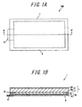
- FIGS. 1(A) and 1(B) illustrate a structural example of a capacitive touch panel 100 according to one of the disclosed embodiments, FIG. 1(A) being a front view of the capacitive touch panel 100, and FIG. 1(B) being a cross-sectional diagram along the AA' line in FIG. 1(A) .
- the capacitive touch panel 100 to which this disclosure is applied includes a top plate 1 which is the upper structure and a sensor 10 that is disposed on the back surface of the top plate 1 and is formed by a transparent electrode layer 8 and a jumper wiring layer 12 provided with an insulating layer.
- the top plate 1 includes a transparent panel substrate 2, a decorative printing layer 5, and a warping prevention layer 7.
- the transparent panel substrate 2 is provided with a transparent resin base 2a that includes resin material with a high heat resistance and a transparent resin layer 2b that includes rigid resin material with a high hardness and is formed on one surface, specifically the front surface, of the transparent resin base 2a.
- the decorative printing layer 5 is formed at the outer edge of the other surface, specifically the back surface, of the transparent resin base 2a.
- the warping prevention layer 7 is formed to cover the decorative printing layer 5 and the back surface of the top plate 1.
- the transparent resin base 2a is preferably formed with PC resin, which is a resin material having a high heat resistance
- the transparent resin layer 2b is preferably formed with PMMA resin, which is a rigid resin material with a high hardness.
- PC resin as a single base has a surface hardness of HB to H and easily scratches.
- PMMA resin has a surface hardness of 3H to 5H and is preferred as a material for the surface of a touch panel.
- the transparent panel substrate 2 constituted by the transparent resin base 2a with the transparent resin layer 2b formed on the surface thereof is formed by simultaneous fusion molding using two types of resin material.
- the decorative printing layer 5 is a layer formed for the purpose of covering a frame region so as not to be visible from the outside.
- the frame region is a region at the outer edge of a liquid crystal screen in a smartphone, tablet, or the like, in which electrodes, wiring, and the like necessary for functioning of the touch panel are formed.
- the decorative printing layer 5 is formed by silkscreen printing to yield multiple layers of repeatedly coated colored ink. In order to apply a predetermined thickness so that the electrodes, wiring, and the like formed in the frame region are not visible, a multilayer printing layer needs to be formed by several applications of a thin application layer, since a thick layer applied only once tends not to be uniform.
- the printing layer is formed by two applications, and in the case of ink with a pale color (such as white) that easily transmits light, approximately four applications are required.
- the thickness per application is approximately 8 ⁇ m
- a layer of pale ink has a thickness of approximately 32 ⁇ m.
- the warping prevention layer 7 is formed to be flat and entirely cover the back surface of the transparent resin base 2a and the decorative printing layer 5.
- a resin material with a coefficient of linear expansion nearly equivalent to the coefficient of linear expansion of the material used in the transparent resin layer 2b formed on the front surface of the transparent resin base 2a is preferably used. Any material may be used in the warping prevention layer 7, such as transparent acrylic resin coating material used in ultraviolet curable ink and heat-curable ink, urethane resin coating material, or the like.
- a coating material containing urethane (meth)acrylate, epoxy (meth)acrylate, polyester (meth)acrylate, polyester urethane (meth)acrylate, polyether (meth)acrylate, polycarbonate (meth)acrylate, polycarbonate urethane (meth)acrylate, or the like may be used. So as not to affect the optical characteristics of the touch panel, the haze, which is the proportion of diffusely transmitted light among all transmitted light, more preferably does not exceed 1%.
- a transparent acrylic or urethane resin coating material or the like with low viscosity allows the level difference occurring between the decorative printing layer 5 and the transparent resin base 2a to be nearly flattened out, and when the transparent electrode layer 8 is connected, a wiring disconnect due to this level difference can be prevented.
- the decorative printing layer 5 has a thickness of approximately 32 ⁇ m. Therefore, it suffices to form the warping prevention layer 7 by applying acrylic coating material across the decorative printing layer 5 and the back surface of the transparent resin base 2a to a thickness of, for example, approximately 35 ⁇ m.
- Another way of applying the acrylic coating material that forms the warping prevention layer 7 is direct application with a die coater. A known application technique may thus be used to form the warping prevention layer 7.
- the same equipment used in the printing process for the decorative printing layer 5 may be used, without the need to install special equipment, thereby allowing a reduction in manufacturing costs.
- the warping prevention layer 7 formed to be flat and entirely cover the back surface of the transparent resin base 2a and the decorative printing layer 5 is for preventing warping, due to ambient temperature, in the transparent panel substrate 2 that has a double layer structure constituted by the transparent resin layer 2b and the transparent resin base 2a, which are formed with two types of resin material.
- the warping prevention layer 7 also functions, however, as a flattening layer that nearly flattens out the level difference occurring between the decorative printing layer 5 and the transparent resin base 2a and that prevents a wiring disconnect due to this level difference when the transparent electrode layer 8 is connected.
- the transparent electrode layer 8 formed below the warping prevention layer 7 is a layer in which transparent electrodes are formed on a transparent film and may include nanowires or nanoparticles formed from any of silver, copper, or their alloys.
- a transparent electrode film with a double layer structure in which electrodes in the x-axis direction and electrodes in the y-axis direction are formed in two films, is generally used.
- the transparent electrode layer 8 may be a single layer, however, by adopting a multilayer structure constituted by a transparent electrode layer 8 that uses Ag nanowires and jumper wiring for identifying the xy coordinates of the transparent electrodes.
- the thickness and the weight of the capacitive touch panel 100 can be reduced, and the number of manufacturing processes can be reduced, thereby allowing a reduction in manufacturing costs. Furthermore, by using an Ag nanowire film, the double layer sensor structure composed of two ITO films that is typically used can be replaced with a single layer structure that is thinner, thus contributing to making the touch panel even thinner and lighter.
- a transparent protective layer 9 is formed on the back surface of the jumper wiring layer 12 so as entirely to cover the surface thereof, except for a thermocompression bonding region of a flexible printed circuit 11 for external connection, and the flexible printed circuit 11 for connecting to an external circuit is connected to the back surface of the jumper wiring layer 12.
- a known material may be used in the transparent protective layer 9, which for example may be formed by applying heat-curable acrylic resin.
- the top plate 1 used in the capacitive touch panel 100 to which this disclosure is applied includes the transparent panel substrate 2 constituted by the transparent resin base 2a and the transparent resin layer 2b, made from a different material, formed on one surface of the transparent resin base 2a; the decorative printing layer 5 formed at an outer edge of a back surface of the transparent panel substrate 2; the warping prevention layer 7, made of transparent resin material having higher heat-resistant temperature characteristics than a thermocompression bonding temperature of the flexible printed circuit 11, formed to be flat and to cover the back surface of the transparent panel substrate 2, on which the decorative printing layer 5 is formed, inside the decorative printing layer 5, and a back surface of the decorative printing layer 5; the transparent electrode layer 8 formed on a back surface of the warping prevention layer 7; the jumper wiring layer 12 provided with an insulating layer and formed on a back surface of the transparent electrode layer 8; and the transparent protective layer 9 formed on the jumper wiring layer 12.
- This capacitive touch panel 100 is manufactured by, for example, performing first through sixth steps (S1 to S6) in accordance with the procedure illustrated in the flowchart of FIG. 2 .
- the decorative printing layer 5 is formed on the flexible transparent panel substrate 2, and the warping prevention layer 7 is formed on the inside of the level difference due to the decorative printing layer 5 on the back surface of the transparent panel substrate 2 and on the back surface of the decorative printing layer 5.
- pressure treatment is applied to the warping prevention layer 7 in a state such that the back surface of the warping prevention layer 7 and the flat surface of a flat substrate 30 are bonded together.
- autoclave treatment is further applied to the warping prevention layer 7 that was subjected to pressure treatment.
- the warping prevention layer 7 that was subjected to autoclave treatment is cured.
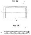
- FIG. 3(A) is a front view of the top plate 1
- FIG. 3(B) is a cross-sectional diagram along the AA' line in FIG. 3(A) .
- the capacitive touch panel 100 is completed by forming the sensor 10 on the back surface of the warping prevention layer 7 of the top plate 1.
- the sensor 10 includes the transparent electrode layer 8 and the jumper wiring layer 12 provided with an insulating layer.
- the decorative printing layer 5 is formed along the perimeter of the flexible transparent panel substrate 2, and the warping prevention layer 7 is formed on the inside of the level difference due to the decorative printing layer 5 on the back surface of the transparent panel substrate 2 and on the back surface of the decorative printing layer 5.
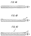
- the decorative printing layer 5 is formed as illustrated in FIG. 4(B) .
- the warping prevention layer 7 is then formed on the transparent panel substrate 2 by printing ultraviolet curable resin, as illustrated in FIG. 4(C) , across the entire inside of the level difference due to the decorative printing layer 5 on the back surface of the transparent panel substrate 2 and across the back surface of the decorative printing layer 5, thereby forming the top plate 1 that includes the transparent panel substrate 2, the decorative printing layer 5, and the warping prevention layer 7.
- the decorative printing layer 5 is a layer formed for the purpose of covering the frame region so as not to be visible from the outside.
- the frame region is a region formed at the outer edge of a liquid crystal screen in a smartphone, tablet, or the like, in which electrodes, wiring, and the like necessary for functioning of the touch panel are formed.
- the decorative printing layer 5 is, for example, formed by silkscreen printing to yield multiple layers of repeatedly coated colored ink.
- a multilayer printing layer needs to be formed by several applications of a thin application layer, since a thick layer applied only once tends not to be uniform.
- the printing layer is formed by two applications, and in the case of ink with a pale color (such as white) that easily transmits light, approximately four applications are required.
- the thickness per application is approximately 8 ⁇ m
- a layer of pale ink has a thickness of approximately 32 ⁇ m.
- pressure treatment is applied to the warping prevention layer 7 in a state such that the back surface of the warping prevention layer 7 and the flat surface of the flat substrate 30 are bonded together.
- a glass plate as the flat substrate 30 is adsorbed on an upper board 20 provided with a suction function, as illustrated in FIG. 5(A) .
- a bonding device is used to sandwich the top plate 1 between the flat substrate 30 and a roller 21 and to roll the roller 21 in the direction of the arrow, thereby bonding the flat substrate 30 and the top plate 1.
- Pressure treatment is thus applied to the warping prevention layer 7 with the roller 21 from the transparent panel substrate 2 side.
- the warping prevention layer 7 may be formed to have a back surface that is a flat surface transferred by pressure treatment and having a maximum unevenness of 0.1 ⁇ m or less.
- autoclave treatment is further applied to the warping prevention layer 7 of the top plate 1 that was subjected to pressure treatment.
- suction of the flat substrate 30 by the upper board 20 is suspended.
- the top plate 1 is removed from the upper board 20 along with the flat substrate 30, placed in an autoclave pressure vessel, and subjected to autoclave treatment.
- the air bubbles remaining in the level difference portion due to the decorative printing layer 5 in the top plate 1 to which pressure treatment has been applied can be further reduced by the application of autoclave treatment, and air bubbles remaining in the image display region on the inside of the decorative printing layer 5 can be eliminated.
- the warping prevention layer 7 of the top plate 1 that was subjected to autoclave treatment is cured.
- the warping prevention layer 7 of the top plate 1 that was subjected to the pressure treatment and the autoclave treatment is irradiated with ultraviolet light from the flat substrate 30 side with an ultraviolet light source 22 to cure the warping prevention layer 7.
- the warping prevention layer 7 can be cured efficiently by irradiation with ultraviolet light from the flat substrate 30 side.
- a polycarbonate base or an acrylic resin base that transmits ultraviolet light and has been subjected to release treatment may be used in the flat substrate 30.
- the flat substrate 30 is peeled off the cured warping prevention layer 7.
- the substrate material is preferably a glass plate with the thickness of 0.5 mm to 2 mm or less and has preferably been subjected to release treatment by applying a water repellent or a release agent to the surface thereof.
- the top plate 1 with the structure illustrated in FIGS. 3(A) and 3(B) is produced by the process from the first through fifth steps (S1 to S5).
- the warping prevention layer 7 is made of transparent resin material that has higher heat-resistant temperature characteristics than the thermocompression bonding temperature of the flexible printed circuit 11, such as an acrylic resin material with a heat-resistant temperature after curing of 140°C or higher.
- the capacitive touch panel 100 is completed.
- the transparent protective layer 9 is formed on the back surface of the jumper wiring layer 12, and the flexible printed circuit 11 for connecting to an external circuit is connected to the back surface of the jumper wiring layer 12.
- a known material may be used in the transparent protective layer 9, which for example may be formed by applying heat-curable or UV-curable acrylic resin.
- Minute resin beads may be mixed into at least one of the warping prevention layer 7 and the transparent protective layer 9 so as to provide a haze of 0.3% or greater.
- the capacitive touch panel samples produced as described below were conserved for 240 hours in a hot-air constant-temperature oven set to 70°C. Subsequently, the capacitive touch panel samples were removed, and warping at both edges of the capacitive touch panel samples after the lapse of predetermined lengths of time at room temperature was measured. The predetermined lengths of time were immediately after removal from the oven, after five minutes, and after one hour.
- Capacitive touch panel sample used for measurement of warping
- Example 1 The sample of Example 1 was produced as follows.
- the resin top plate base (MRS58W, 297 mm ⁇ 210 mm ⁇ 0.8 mm, produced by Mitsubishi Gas Chemical) was subjected to silkscreen printing (mesh #200) using MRX-HF919 black (produced by Teikoku Printing Inks Mfg.) and then dried and cured for one hour at 80°C to form a decorative printing layer with a thickness of 8 ⁇ m.
- 0.2 parts by weight of transparent resin filler were dispersed per 100 parts by weight of transparent ink (RL-9262), and the resulting material was used to perform silkscreen printing (mesh #200) on the decorative printing layer to form a warping prevention layer over the entire back surface of the resin top plate including the decorative printing layer.
- the thickness of the warping prevention layer at this time was approximately 12 ⁇ m.
- an insulating layer and jumper wires were disposed to form a second transparent electrode layer.
- transparent resin material FR-1TNSD9 was applied over the entire transparent electrode layer to form a transparent protective layer.
- the prepared capacitive touch panel sample was then conserved for 240 hours in a hot-air constant-temperature oven at 70°C, and the warping of the base upon removal was measured.
- Table 1 Warping at time of heating to 70°C and conserving Initial stage mm 70°C, conservation for 240 hours, time after removal, mm immediately after 5 minutes 1 hour Conventional Example 0.3 -4.3 0.4 0.2 Example 1 0 1.3 0.0 0.0
- the vertical axis in the graph in FIG. 6 indicates the amount of warping of the base.
- the sign of the warping is as illustrated in FIGS. 7A and 7B .
- the bar graph indicates the length of time elapsed for the warping: immediately after removal from the state of conservation, and the values measured after sitting at room temperature for five minutes and for one hour.
- the sample to the left is the capacitive touch panel sample of the Conventional Example, and the sample to the right is the capacitive touch panel sample of Example 1.
- Example 1 of this disclosure was reduced in Example 1 of this disclosure to approximately one fourth of the amount of warping of the Conventional Example.
- Capacitive touch panel sample used for measurement of haze (degree of cloudiness) of warping prevention layer and visibility of transparent electrode layer
- the capacitive touch panel sample was prepared in a similar way to Example 1, except for using MR-20G (average particle size of 20 ⁇ m, Soken Chemical & Engineering) as the transparent resin filler mixed into the transparent ink forming the warping prevention layer and dispersing 10 parts by weight of the transparent resin filler per 100 parts by weight of the transparent ink.
- MR-20G average particle size of 20 ⁇ m, Soken Chemical & Engineering
- Capacitive touch panel sample used for measurement of haze (degree of cloudiness) of warping prevention layer and visibility of transparent electrode layer
- the capacitive touch panel sample was prepared in a similar way to Example 1, except for using MR-10G (average particle size of 9 ⁇ m, Soken Chemical & Engineering) as the transparent resin filler mixed into the transparent ink forming the warping prevention layer and dispersing 1 part by weight of the transparent resin filler per 100 parts by weight of the transparent ink.
- MR-10G average particle size of 9 ⁇ m, Soken Chemical & Engineering
- Capacitive touch panel sample used for measurement of haze (degree of cloudiness) of warping prevention layer and visibility of transparent electrode layer
- the capacitive touch panel sample was prepared in a similar way to Example 1, except for not mixing transparent resin filler into the transparent ink forming the warping prevention layer.
- Table 2 below shows the results of measuring haze (degree of cloudiness) of the warping prevention layer and visibility of the transparent electrode layer for Examples 1 to 3 and the Comparative Example.
- Table 2 Haze (degree of cloudiness) of warping prevention layer and visibility of transparent electrodes Transparent resin filler % of haze (degree of cloudiness) Visibility of transparent conductive layer average particle size ⁇ m parts by weight Example 1 3 0.2 0.3 not visible Example 2 20 10 4.9 not visible Example 3 9 1 2.1 not visible Comparative Example none 0.18 visible
- the transparent electrode layer is formed from silver nanowire ink, and the reflectance of incident light from the resin top plate surface differs between the electrode portion, which contains silver nanowires, and the insulating portion, which does not. Therefore, the electrode portion becomes visible. It is clear that when the haze of the warping prevention layer is 0.3% or greater, as in Examples 1 to 3, the transparent electrode layer formed thereon is not visible.
- Table 3 lists the results of measuring visibility of the compression mark from thermal deformation of the base due to the compression jig when the substrate for external connection, i.e. the Flexible Printed Circuit (FPC) 11, was subjected to thermocompression bonding.
- FPC Flexible Printed Circuit
- Table 3 Visibility of deformation in FPC thermocompressed portion Base name Thickness mm Deformation of thermocompressed portion (conditions: 150°C, 10 s) Notes Example 1 0.8 good two-type, two-layer product PMMA 1 poor Comparative Example: single-layer product PMMA/PC /PMMA 0.8 average Comparative Example: two-type, three-layer product
- the temperature of the compression jig was 150°C, the pressure was approximately 4 MPa, and the compression time was 10 s.
- touch panels were prepared to have a similar structure to that of Example 1, except for using the below-described bases and not forming a warping prevention layer.
- the portion contacted by the FPC thermocompression jig was the warping prevention layer (UV curable acrylic resin) in Example 1 and the PMMA resin layer in the PMMA (single layer) and PMMA/PC/PMMA (two type, three layer) of the Comparative Examples.
- the heat resistance of these contacted portions was affected by the state of thermal deformation.
- the warping prevention layer of Example 1 has sufficient heat resistance, no deformation occurs at the compressed portion of the FPC, and the compression mark is not visible from the resin top plate surface. Accordingly, a good resin top plate can be provided as the touch panel of this disclosure.
Landscapes
- Engineering & Computer Science (AREA)
- General Engineering & Computer Science (AREA)
- Theoretical Computer Science (AREA)
- Human Computer Interaction (AREA)
- Physics & Mathematics (AREA)
- General Physics & Mathematics (AREA)
- Position Input By Displaying (AREA)
- Laminated Bodies (AREA)
Applications Claiming Priority (2)
| Application Number | Priority Date | Filing Date | Title |
|---|---|---|---|
| JP2013185530A JP5848736B2 (ja) | 2013-09-06 | 2013-09-06 | 静電容量型タッチパネル |
| PCT/JP2014/004562 WO2015033569A1 (fr) | 2013-09-06 | 2014-09-04 | Panneau tactile capacitif |
Publications (2)
| Publication Number | Publication Date |
|---|---|
| EP3043242A1 true EP3043242A1 (fr) | 2016-07-13 |
| EP3043242A4 EP3043242A4 (fr) | 2017-05-10 |
Family
ID=52628065
Family Applications (1)
| Application Number | Title | Priority Date | Filing Date |
|---|---|---|---|
| EP14841568.0A Withdrawn EP3043242A4 (fr) | 2013-09-06 | 2014-09-04 | Panneau tactile capacitif |
Country Status (7)
| Country | Link |
|---|---|
| US (1) | US20160202801A1 (fr) |
| EP (1) | EP3043242A4 (fr) |
| JP (1) | JP5848736B2 (fr) |
| KR (1) | KR20160053923A (fr) |
| CN (1) | CN105518592A (fr) |
| TW (1) | TW201523377A (fr) |
| WO (1) | WO2015033569A1 (fr) |
Cited By (8)
| Publication number | Priority date | Publication date | Assignee | Title |
|---|---|---|---|---|
| WO2018106176A1 (fr) * | 2016-12-07 | 2018-06-14 | Flatfrog Laboratories Ab | Dispositif tactile amélioré |
| US11893189B2 (en) | 2020-02-10 | 2024-02-06 | Flatfrog Laboratories Ab | Touch-sensing apparatus |
| US12055969B2 (en) | 2018-10-20 | 2024-08-06 | Flatfrog Laboratories Ab | Frame for a touch-sensitive device and tool therefor |
| US12056316B2 (en) | 2019-11-25 | 2024-08-06 | Flatfrog Laboratories Ab | Touch-sensing apparatus |
| US12086362B2 (en) | 2017-09-01 | 2024-09-10 | Flatfrog Laboratories Ab | Optical component |
| US12175044B2 (en) | 2017-02-06 | 2024-12-24 | Flatfrog Laboratories Ab | Optical coupling in touch-sensing systems |
| US12282653B2 (en) | 2020-02-08 | 2025-04-22 | Flatfrog Laboratories Ab | Touch apparatus with low latency interactions |
| US12524116B2 (en) | 2018-03-05 | 2026-01-13 | Flatfrog Laboratories Ab | Detection line broadening |
Families Citing this family (6)
| Publication number | Priority date | Publication date | Assignee | Title |
|---|---|---|---|---|
| JP2016173736A (ja) * | 2015-03-17 | 2016-09-29 | アルプス電気株式会社 | センサーパネル及びセンサーパネルの製造方法 |
| CN104994318A (zh) * | 2015-07-28 | 2015-10-21 | 张家港保税区佰昂特种玻璃有限公司 | 一种热敏电视触屏 |
| KR20170018718A (ko) * | 2015-08-10 | 2017-02-20 | 삼성전자주식회사 | 비정질 합금을 이용한 투명 전극 및 그 제조 방법 |
| JP6554365B2 (ja) * | 2015-09-04 | 2019-07-31 | アルプスアルパイン株式会社 | 外装パネルの製造方法 |
| KR102512276B1 (ko) * | 2016-03-07 | 2023-03-22 | 삼성디스플레이 주식회사 | 합착장치 및 이를 이용한 합착방법 |
| CN106020554A (zh) * | 2016-06-06 | 2016-10-12 | 京东方科技集团股份有限公司 | 触控盖板及其制造方法和触控显示装置 |
Family Cites Families (12)
| Publication number | Priority date | Publication date | Assignee | Title |
|---|---|---|---|---|
| JP4435890B2 (ja) | 1999-01-12 | 2010-03-24 | 日本写真印刷株式会社 | タッチパネル |
| JP2003045234A (ja) * | 2001-07-26 | 2003-02-14 | Dainippon Printing Co Ltd | 透明導電性フィルム |
| CN100478711C (zh) * | 2004-10-15 | 2009-04-15 | 三菱丽阳株式会社 | 活性能线固化型树脂组合物以及片状光学物品 |
| WO2008089401A2 (fr) * | 2007-01-18 | 2008-07-24 | Arizona Board Of Regents, Acting For And On Behalfof Arizona State University | Électrodes transparentes flexibles via des nanofils et une couche conductrice sacrificielle |
| TWM348999U (en) | 2008-02-18 | 2009-01-11 | Tpk Touch Solutions Inc | Capacitive touch panel |
| JP2012125991A (ja) * | 2010-12-15 | 2012-07-05 | Nitto Denko Corp | 積層体 |
| JP2012209030A (ja) * | 2011-03-29 | 2012-10-25 | Toray Advanced Film Co Ltd | 透明導電積層体およびその製造方法 |
| JP5651526B2 (ja) * | 2011-04-28 | 2015-01-14 | 藤森工業株式会社 | ハードコートフィルム及びそれを用いたタッチパネル |
| CN102929454A (zh) * | 2011-08-12 | 2013-02-13 | 宸鸿科技(厦门)有限公司 | 电容式触控面板及降低其金属导体可见度的方法 |
| JP2013127546A (ja) * | 2011-12-19 | 2013-06-27 | Panasonic Corp | 透明電極付き反射防止フィルム |
| JP5671485B2 (ja) * | 2012-01-11 | 2015-02-18 | 綜研化学株式会社 | 導電膜用粘着テープおよびタッチパネル用積層体 |
| JP5869591B2 (ja) * | 2012-01-25 | 2016-02-24 | 京セラ株式会社 | 入力装置、表示装置、および電子機器 |
-
2013
- 2013-09-06 JP JP2013185530A patent/JP5848736B2/ja active Active
-
2014
- 2014-09-04 WO PCT/JP2014/004562 patent/WO2015033569A1/fr not_active Ceased
- 2014-09-04 US US14/915,960 patent/US20160202801A1/en not_active Abandoned
- 2014-09-04 KR KR1020167005768A patent/KR20160053923A/ko not_active Withdrawn
- 2014-09-04 CN CN201480048807.0A patent/CN105518592A/zh active Pending
- 2014-09-04 EP EP14841568.0A patent/EP3043242A4/fr not_active Withdrawn
- 2014-09-05 TW TW103130779A patent/TW201523377A/zh unknown
Non-Patent Citations (2)
| Title |
|---|
| No further relevant documents disclosed * |
| See also references of WO2015033569A1 * |
Cited By (11)
| Publication number | Priority date | Publication date | Assignee | Title |
|---|---|---|---|---|
| WO2018106176A1 (fr) * | 2016-12-07 | 2018-06-14 | Flatfrog Laboratories Ab | Dispositif tactile amélioré |
| US10282035B2 (en) | 2016-12-07 | 2019-05-07 | Flatfrog Laboratories Ab | Touch device |
| US12175044B2 (en) | 2017-02-06 | 2024-12-24 | Flatfrog Laboratories Ab | Optical coupling in touch-sensing systems |
| US12524117B2 (en) | 2017-02-06 | 2026-01-13 | Flatfrog Laboratories Ab | Optical coupling in touch-sensing systems |
| US12086362B2 (en) | 2017-09-01 | 2024-09-10 | Flatfrog Laboratories Ab | Optical component |
| US12524116B2 (en) | 2018-03-05 | 2026-01-13 | Flatfrog Laboratories Ab | Detection line broadening |
| US12055969B2 (en) | 2018-10-20 | 2024-08-06 | Flatfrog Laboratories Ab | Frame for a touch-sensitive device and tool therefor |
| US12056316B2 (en) | 2019-11-25 | 2024-08-06 | Flatfrog Laboratories Ab | Touch-sensing apparatus |
| US12461630B2 (en) | 2019-11-25 | 2025-11-04 | Flatfrog Laboratories Ab | Touch-sensing apparatus |
| US12282653B2 (en) | 2020-02-08 | 2025-04-22 | Flatfrog Laboratories Ab | Touch apparatus with low latency interactions |
| US11893189B2 (en) | 2020-02-10 | 2024-02-06 | Flatfrog Laboratories Ab | Touch-sensing apparatus |
Also Published As
| Publication number | Publication date |
|---|---|
| EP3043242A4 (fr) | 2017-05-10 |
| JP5848736B2 (ja) | 2016-01-27 |
| KR20160053923A (ko) | 2016-05-13 |
| WO2015033569A1 (fr) | 2015-03-12 |
| US20160202801A1 (en) | 2016-07-14 |
| TW201523377A (zh) | 2015-06-16 |
| JP2015052916A (ja) | 2015-03-19 |
| CN105518592A (zh) | 2016-04-20 |
Similar Documents
| Publication | Publication Date | Title |
|---|---|---|
| EP3043242A1 (fr) | Panneau tactile capacitif | |
| TW201514820A (zh) | 靜電電容型曲面形狀觸控面板及其製造方法 | |
| EP3264236B1 (fr) | Écran à cristaux liquides intégré entièrement scellé et son procédé de fabrication | |
| US20040017363A1 (en) | Touch panel and electronic apparatus using the same | |
| EP3037928A1 (fr) | Panneau tactile capacitif et son procédé de fabrication | |
| CN104345962A (zh) | 便携式电子产品、触摸屏及触摸屏制备方法 | |
| JP5795357B2 (ja) | 静電容量型タッチパネル | |
| KR20140052510A (ko) | 터치스크린 패널의 제조 방법 | |
| JP5860837B2 (ja) | 静電容量型タッチパネル | |
| TW201539279A (zh) | 積層體、積層體之製造方法、靜電容型觸控面板及影像顯示裝置 | |
| CN106471448A (zh) | 层叠体、层叠体的制造方法、静电电容型触控面板和图像显示装置 | |
| KR101537161B1 (ko) | 검지 기능을 갖는 표면 패널 및 그 제조 방법 | |
| CN110381687A (zh) | 装饰膜片及壳体组件和电子设备 | |
| CN111161638A (zh) | 一种多层柔性显示屏组件及其制作方法 | |
| JP5856114B2 (ja) | 静電容量型タッチパネルの製造方法 | |
| CN120279814A (zh) | 显示模组以及显示装置 | |
| JP2015095022A (ja) | 静電容量型タッチパネル |
Legal Events
| Date | Code | Title | Description |
|---|---|---|---|
| PUAI | Public reference made under article 153(3) epc to a published international application that has entered the european phase |
Free format text: ORIGINAL CODE: 0009012 |
|
| 17P | Request for examination filed |
Effective date: 20160302 |
|
| AK | Designated contracting states |
Kind code of ref document: A1 Designated state(s): AL AT BE BG CH CY CZ DE DK EE ES FI FR GB GR HR HU IE IS IT LI LT LU LV MC MK MT NL NO PL PT RO RS SE SI SK SM TR |
|
| AX | Request for extension of the european patent |
Extension state: BA ME |
|
| DAX | Request for extension of the european patent (deleted) | ||
| A4 | Supplementary search report drawn up and despatched |
Effective date: 20170410 |
|
| RIC1 | Information provided on ipc code assigned before grant |
Ipc: G06F 3/044 20060101ALI20170404BHEP Ipc: G06F 3/041 20060101AFI20170404BHEP |
|
| STAA | Information on the status of an ep patent application or granted ep patent |
Free format text: STATUS: THE APPLICATION IS DEEMED TO BE WITHDRAWN |
|
| 18D | Application deemed to be withdrawn |
Effective date: 20171109 |