EP3043477B1 - Vorrichtungen und verfahren zur takt- und datenrückgewinnung - Google Patents
Vorrichtungen und verfahren zur takt- und datenrückgewinnung Download PDFInfo
- Publication number
- EP3043477B1 EP3043477B1 EP16150636.5A EP16150636A EP3043477B1 EP 3043477 B1 EP3043477 B1 EP 3043477B1 EP 16150636 A EP16150636 A EP 16150636A EP 3043477 B1 EP3043477 B1 EP 3043477B1
- Authority
- EP
- European Patent Office
- Prior art keywords
- phase
- signal
- master
- cdr
- circuit
- Prior art date
- Legal status (The legal status is an assumption and is not a legal conclusion. Google has not performed a legal analysis and makes no representation as to the accuracy of the status listed.)
- Active
Links
Images


Classifications
-
- G—PHYSICS
- G06—COMPUTING OR CALCULATING; COUNTING
- G06F—ELECTRIC DIGITAL DATA PROCESSING
- G06F13/00—Interconnection of, or transfer of information or other signals between, memories, input/output devices or central processing units
- G06F13/38—Information transfer, e.g. on bus
- G06F13/40—Bus structure
- G06F13/4063—Device-to-bus coupling
- G06F13/4068—Electrical coupling
-
- H—ELECTRICITY
- H04—ELECTRIC COMMUNICATION TECHNIQUE
- H04L—TRANSMISSION OF DIGITAL INFORMATION, e.g. TELEGRAPHIC COMMUNICATION
- H04L7/00—Arrangements for synchronising receiver with transmitter
- H04L7/02—Speed or phase control by the received code signals, the signals containing no special synchronisation information
- H04L7/033—Speed or phase control by the received code signals, the signals containing no special synchronisation information using the transitions of the received signal to control the phase of the synchronising-signal-generating means, e.g. using a phase-locked loop
- H04L7/0337—Selecting between two or more discretely delayed clocks or selecting between two or more discretely delayed received code signals
-
- G—PHYSICS
- G06—COMPUTING OR CALCULATING; COUNTING
- G06F—ELECTRIC DIGITAL DATA PROCESSING
- G06F13/00—Interconnection of, or transfer of information or other signals between, memories, input/output devices or central processing units
- G06F13/38—Information transfer, e.g. on bus
- G06F13/42—Bus transfer protocol, e.g. handshake; Synchronisation
- G06F13/4282—Bus transfer protocol, e.g. handshake; Synchronisation on a serial bus, e.g. I2C bus, SPI bus
- G06F13/4291—Bus transfer protocol, e.g. handshake; Synchronisation on a serial bus, e.g. I2C bus, SPI bus using a clocked protocol
-
- H—ELECTRICITY
- H03—ELECTRONIC CIRCUITRY
- H03L—AUTOMATIC CONTROL, STARTING, SYNCHRONISATION OR STABILISATION OF GENERATORS OF ELECTRONIC OSCILLATIONS OR PULSES
- H03L7/00—Automatic control of frequency or phase; Synchronisation
- H03L7/06—Automatic control of frequency or phase; Synchronisation using a reference signal applied to a frequency- or phase-locked loop
- H03L7/07—Automatic control of frequency or phase; Synchronisation using a reference signal applied to a frequency- or phase-locked loop using several loops, e.g. for redundant clock signal generation
-
- H—ELECTRICITY
- H03—ELECTRONIC CIRCUITRY
- H03L—AUTOMATIC CONTROL, STARTING, SYNCHRONISATION OR STABILISATION OF GENERATORS OF ELECTRONIC OSCILLATIONS OR PULSES
- H03L7/00—Automatic control of frequency or phase; Synchronisation
- H03L7/06—Automatic control of frequency or phase; Synchronisation using a reference signal applied to a frequency- or phase-locked loop
- H03L7/08—Details of the phase-locked loop
- H03L7/0807—Details of the phase-locked loop concerning mainly a recovery circuit for the reference signal
-
- H—ELECTRICITY
- H03—ELECTRONIC CIRCUITRY
- H03L—AUTOMATIC CONTROL, STARTING, SYNCHRONISATION OR STABILISATION OF GENERATORS OF ELECTRONIC OSCILLATIONS OR PULSES
- H03L7/00—Automatic control of frequency or phase; Synchronisation
- H03L7/06—Automatic control of frequency or phase; Synchronisation using a reference signal applied to a frequency- or phase-locked loop
- H03L7/08—Details of the phase-locked loop
- H03L7/081—Details of the phase-locked loop provided with an additional controlled phase shifter
- H03L7/0812—Details of the phase-locked loop provided with an additional controlled phase shifter and where no voltage or current controlled oscillator is used
- H03L7/0814—Details of the phase-locked loop provided with an additional controlled phase shifter and where no voltage or current controlled oscillator is used the phase shifting device being digitally controlled
-
- H—ELECTRICITY
- H03—ELECTRONIC CIRCUITRY
- H03L—AUTOMATIC CONTROL, STARTING, SYNCHRONISATION OR STABILISATION OF GENERATORS OF ELECTRONIC OSCILLATIONS OR PULSES
- H03L7/00—Automatic control of frequency or phase; Synchronisation
- H03L7/06—Automatic control of frequency or phase; Synchronisation using a reference signal applied to a frequency- or phase-locked loop
- H03L7/08—Details of the phase-locked loop
- H03L7/085—Details of the phase-locked loop concerning mainly the frequency- or phase-detection arrangement including the filtering or amplification of its output signal
- H03L7/087—Details of the phase-locked loop concerning mainly the frequency- or phase-detection arrangement including the filtering or amplification of its output signal using at least two phase detectors or a frequency and phase detector in the loop
-
- H—ELECTRICITY
- H03—ELECTRONIC CIRCUITRY
- H03L—AUTOMATIC CONTROL, STARTING, SYNCHRONISATION OR STABILISATION OF GENERATORS OF ELECTRONIC OSCILLATIONS OR PULSES
- H03L7/00—Automatic control of frequency or phase; Synchronisation
- H03L7/06—Automatic control of frequency or phase; Synchronisation using a reference signal applied to a frequency- or phase-locked loop
- H03L7/08—Details of the phase-locked loop
- H03L7/085—Details of the phase-locked loop concerning mainly the frequency- or phase-detection arrangement including the filtering or amplification of its output signal
- H03L7/091—Details of the phase-locked loop concerning mainly the frequency- or phase-detection arrangement including the filtering or amplification of its output signal the phase or frequency detector using a sampling device
-
- H—ELECTRICITY
- H04—ELECTRIC COMMUNICATION TECHNIQUE
- H04L—TRANSMISSION OF DIGITAL INFORMATION, e.g. TELEGRAPHIC COMMUNICATION
- H04L25/00—Baseband systems
- H04L25/02—Details ; arrangements for supplying electrical power along data transmission lines
- H04L25/14—Channel dividing arrangements, i.e. in which a single bit stream is divided between several baseband channels and reassembled at the receiver
-
- H—ELECTRICITY
- H04—ELECTRIC COMMUNICATION TECHNIQUE
- H04L—TRANSMISSION OF DIGITAL INFORMATION, e.g. TELEGRAPHIC COMMUNICATION
- H04L7/00—Arrangements for synchronising receiver with transmitter
- H04L7/0016—Arrangements for synchronising receiver with transmitter correction of synchronization errors
- H04L7/002—Arrangements for synchronising receiver with transmitter correction of synchronization errors correction by interpolation
-
- H—ELECTRICITY
- H04—ELECTRIC COMMUNICATION TECHNIQUE
- H04L—TRANSMISSION OF DIGITAL INFORMATION, e.g. TELEGRAPHIC COMMUNICATION
- H04L7/00—Arrangements for synchronising receiver with transmitter
- H04L7/0016—Arrangements for synchronising receiver with transmitter correction of synchronization errors
- H04L7/0033—Correction by delay
-
- H—ELECTRICITY
- H04—ELECTRIC COMMUNICATION TECHNIQUE
- H04L—TRANSMISSION OF DIGITAL INFORMATION, e.g. TELEGRAPHIC COMMUNICATION
- H04L7/00—Arrangements for synchronising receiver with transmitter
- H04L7/02—Speed or phase control by the received code signals, the signals containing no special synchronisation information
-
- H—ELECTRICITY
- H04—ELECTRIC COMMUNICATION TECHNIQUE
- H04L—TRANSMISSION OF DIGITAL INFORMATION, e.g. TELEGRAPHIC COMMUNICATION
- H04L7/00—Arrangements for synchronising receiver with transmitter
- H04L7/04—Speed or phase control by synchronisation signals
- H04L7/041—Speed or phase control by synchronisation signals using special codes as synchronising signal
- H04L7/042—Detectors therefor, e.g. correlators, state machines
-
- G—PHYSICS
- G06—COMPUTING OR CALCULATING; COUNTING
- G06F—ELECTRIC DIGITAL DATA PROCESSING
- G06F2213/00—Indexing scheme relating to interconnection of, or transfer of information or other signals between, memories, input/output devices or central processing units
- G06F2213/0002—Serial port, e.g. RS232C
-
- H—ELECTRICITY
- H04—ELECTRIC COMMUNICATION TECHNIQUE
- H04L—TRANSMISSION OF DIGITAL INFORMATION, e.g. TELEGRAPHIC COMMUNICATION
- H04L7/00—Arrangements for synchronising receiver with transmitter
- H04L7/0008—Synchronisation information channels, e.g. clock distribution lines
Definitions
- Embodiments of the invention relate to electronic devices, and more particularly, to clock and data recovery circuits.
- Clock and data recovery (CDR) circuits can be used in a variety of applications for recovering data from a high-speed serial data stream.
- a chip-to-chip communication system can include two or more serial communication links or lanes used to communicate data from a first integrated circuit (IC) or chip to a second IC.
- each lane can include a CDR circuit for recovering data from an input data stream received over the lane.
- the chip-to-chip communication system can exhibit a higher overall data rate relative to a configuration using a single lane.
- US 2006/0224339 discloses a clock and data recovery system where a first CDR unit acts as a "master” to generate synchronous clocking signals that are provided to "slave” circuits by way of an interconnect.
- US 7,139,348 discloses a circuit where a plurality of slave DLLs are connected to a shared clock tree. One of the DLLs act as a master to recover the clock signal and sends calibration information to each of the slave DLLs.
- the slave DLLs only include data DLLs.
- EP 1067742 discloses a system in which a symmetric differential phase shift keying communication system, input phases ⁇ k to ⁇ k-3 are provided to a phase difference encoder to generate a receiver vector.
- a clock and data recovery (CDR) system is provided as claimed in claim 1.
- a chip-to-chip communication system includes two or more CDR circuits that recover data from two or more serial data communication links or lanes.
- a first CDR circuit receives a first input data stream from a first lane, and captures data samples and edge samples from the first input data stream. The data samples and edge samples are used to generate a master phase signal, which the first CDR circuit uses to control a phase of a data sampling clock signal used for capturing the data samples from the first input data stream.
- the first CDR circuit generates a master phase error signal based on changes to the master phase signal over time, and the first CDR circuit forwards the master phase error signal to at least a second CDR circuit.
- the second CDR circuit processes the master phase error signal to generate a slave phase signal that is used to control a phase of a data sampling clock signal used for capturing data samples from a second input data stream received over a second lane.
- the power consumption of the chip-to-chip communication system can be reduced.
- edge sampling and/or delay-locked loop circuitry of the slave CDR circuit can be powered off to reduce power consumption.
- the master phase error signal can be encoded using a phase difference encoder. Additionally, the encoded master phase error signal can be sent to one or more slave CDR circuits that include a phase difference decoder for decoding the encoded master phase error signal.
- a timing constraint between a master CDR circuit and a slave CDR circuit can be relaxed or eliminated.
- the master CDR circuit and one or more slave CDR circuits can operate in parallel to track incoming data received on the lanes.
- the lanes each carry distinct data and none are redundant versions of another lane. Random jitter among the lanes can be correlated, which permits the slave CDR circuits to track phase changes in the master CDR circuit while maintaining lock with received input data streams.
- the correlation in jitter can arise from a common jitter source, such as a clock multiplier unit that generates reference clock signals for both circuitry that transmits data on the lanes and for CDR circuits that recover data from the lanes.
- a slave CDR circuit can include a jitter coherence determination circuit to determine whether or not the jitter between a master CDR circuit and the slave CDR circuit is coherent. Additionally, when the jitter is determined to be incoherent, the slave CDR circuit can recover incoming data using separate phase information from the master CDR circuit.
- the slave CDR circuits can operate with a phase offset relative to the master phase signal.
- the phase offset can be separately selected for each slave CDR circuit to enhance data tracking performance.
- the phase offset can be regularly calibrated or updated to prevent the slave CDR circuit from losing lock in the presence of phase drift.
- two or more CDR circuits can employ a token passing scheme to control timing of phase offset calibrations. When a particular slave CDR circuit holds the token, the slave CDR circuit can track incoming data using separate phase information from the master CDR circuit and can observe a difference between the local phase information and the master phase information to calibrate the slave CDR circuit's phase offset.
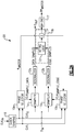
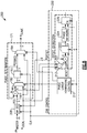
- FIG. 1 is a schematic diagram of one embodiment of a chip-to-chip communication system 10.
- the chip-to-chip communication system 10 includes a first integrated circuit (IC) or chip 1 and a second IC 2.
- the chip-to-chip communication system 10 illustrates one example of a chip-to-chip communication system in accordance with the teachings herein.
- a chip-to-chip communication system can use two or more serial communication links or lanes to increase an overall data rate.
- a chip-to-chip communication system that includes 8 lanes that each operate at 12.5 Gb/s can have an overall data rate of about 100 Gb/s.
- the chip-to-chip communication system 10 includes a first lane 9a, a second lane 9b, and a third lane 9c. Although the chip-to-chip communication system 10 is illustrated as including three lanes, the chip-to-chip communication system 10 can include more or fewer lanes. For example, in one embodiment, the chip-to-chip communication system 10 includes between 2 and 8 lanes.
- Aggregate data rates between ICs of a chip-to-chip communication system can be relatively high.
- a chip-to-chip communication system may operate at 100 Gb/s or more.
- it can be desirable to lower power consumption to decrease heat dissipation and/or increase the range of temperatures that the ICs can operate over.
- the first IC 1 includes a first phase-locked loop (PLL) 3, a first transmitter 4a, a second transmitter 4b, and a third transmitter 4c.
- the first PLL 3 receives a reference clock signal CLK REF , and generates a transmit clock signal CLK TX .
- the first to third transmitters 4a-4c can use the transmit clock signal CLK TX to control timing of data transmissions over the first to third lanes 9a-9c.
- the first to third lanes 9a-9c operate as conductive pathways used to electrically transmit streams of data between the first and second ICs 1, 2.
- the first to third lanes 9a-9c can include printed circuit board (PCB) trace, vias, and/or other conductive structures used to provide electrical connections between the first and second ICs 1, 2.
- PCB printed circuit board
- the second IC 2 includes a second PLL 5, a first equalizer 6a, a second equalizer 6b, a third equalizer 6c, a first clock and data recovery (CDR) circuit 7a, a second CDR circuit 7b, and a third CDR circuit 7c.
- the first equalizer 6a can be used to equalize a first input data signal or stream received over the first lane 9a.
- the second equalizer 6b can be used to equalize a second input data stream received over the second lane 9b
- the third equalizer 6c can be used to equalize a third input data stream received over the third lane 9c.
- the first to third equalizers 6a-6c can be used to provide signal equalization to compensate for losses of the first to third lanes 9a-9c, respectively.
- an equalizer can be used to compensate for high-frequency signal loss by boosting high frequency components of a signal relative to low frequency components of the signal, thereby improving signal fidelity.
- the second PLL 5 receives the reference clock signal CLK REF and generates a receive clock signal CLK RX .
- the first CDR circuit 7a receives the first input data stream over the first lane 9a and generates a first output data signal D OUT1 .
- the second CDR circuit 7b receives the second input data stream over the second lane 9b and generates a second output data signal D OUT2
- the third CDR circuit 7c receives the third input data stream over the third lane 9c and generates a third output data signal D OUT3 .
- the chip-to-chip communication system 10 communicates over the lanes 9a-9c, which may have correlated jitter.
- both the first IC 1 and the second IC 2 receive the reference clock signal CLK REF .
- jitter of the reference clock signal CLK REF may generate correlated jitter in sampling clock signals of the CDR circuits 7a-7c used to recover data from the lanes 9a-9c.
- the first to third CDR circuits 7a-7c can track the incoming data received on the lanes 9a-9c to mitigate jitter, such as jitter associated with electromagnetic interference (EMI), coupling, and/or supply switching.
- jitter such as jitter associated with electromagnetic interference (EMI), coupling, and/or supply switching.
- EMI electromagnetic interference
- the first CDR circuit 7a can capture data samples and edge samples from the first input data stream received over the first lane 9a. Additionally, the first CDR circuit 7a can generate a master phase signal based on the data samples and the edge samples, and can use the master phase signal to control a phase of a data sampling clock signal used to capture the data samples from the first input data stream.
- the first CDR circuit 7a also generates a master phase error signal ⁇ MASTER , which can be based on a change of the master phase signal over time.
- the master phase error signal ⁇ MASTER corresponds to a difference between the master phase signal and a delayed version of the master phase signal, such as a master phase signal delayed by one or more cycles of the receive clock signal CLK RX or a divided version thereof.
- other configurations are possible.
- the master phase error signal ⁇ MASTER is provided to the second and third CDR circuits 7b, 7c, which process the master phase error signal ⁇ MASTER to control phases of second and third data sampling clock signals used to sample the second and third input data streams received over the second and third lanes 9b, 9c, respectively.
- the illustrated chip-to-chip communication system 10 illustrates one example of an electronic system that can employ phase error forwarding.
- a phase error from a master CDR circuit can be forwarded to one or more slave CDR circuits. Additionally, the master phase error can be processed by the slave CDR circuits, thereby permitting portions of the slave CDR circuits to be powered down for energy efficient data recovery.
- the illustrated chip-to-chip communication system 10 uses a phase error forwarding technique to share phase information among parallel lanes.
- the first CDR circuit 7a can generate the master phase error signal ⁇ MASTER to keep the second and third CDR circuits 7b, 7c in phase-lock.
- the illustrated configuration can maintain the benefits of clock and data recovery, such as high-pass filtering of jitter, with reduced power consumption.
- the first CDR circuit 7a can broadcast or forward phase updates or changes to the second and third CDR circuits 7b, 7c using the master phase error signal ⁇ MASTER .
- the second and third CDR circuits 7b, 7c can use the master phase error signal ⁇ MASTER to control data sampling operations of the input data streams received by the second and third CDR circuits 7b, 7c.
- the master phase error signal ⁇ MASTER can be forwarded using an encryption or encoding scheme that allows for phase error updates to be communicated between lanes without stringent specifications related to timing synchronization.
- the edge sampler of any disabled CDR circuits can be used for other functions of the chip-to-chip communication system 10.
- the edge sampler of a disabled slave CDR circuit can be used as a real-time eye opening monitor.
- the first IC 1 and the second IC 2 can correspond to ICs of a wide variety of types.
- the first IC 1 comprises a field programmable gate array (FPGA) and the second IC 2 comprises a digital-to-analog converter (DAC).
- the first IC 1 comprises a microprocessor and the second IC 2 comprises a microprocessor peripheral.
- the chip-to-chip communication system 10 can use phase error forwarding, in certain configurations the phase error forwarding can be applied only for certain time intervals and/or between certain CDR circuits.
- the chip-to-chip communication system 10 may operate over an initialization phase in which the first to third CDR circuits 7a-7c track incoming data using separate phase information to determine a phase offset of the second and third CDR circuits 7b, 7c relative to the first CDR circuit 7a. Thereafter, the chip-to-chip communication system 10 may operate over a tracking phase in which the second and third CDR circuits 7b, 7c track or follow the master phase error signal ⁇ MASTER forwarded by the first CDR circuit 7a.
- edge tracking circuitry of the second and/or third CDR circuits 7b, 7c can be regularly re-enabled and used in part to generate local phase information for updating the phase offset.
- the chip-to-chip communication system 10 can employ a token passing scheme in which the second and third CDR circuits 7b, 7c and/or any additional slave CDR circuits pass a token to determine when a particular slave CDR circuit is calibrated to update phase offset. Configuring the slave CDR circuits in this manner can help prevent the slave CDR circuits from losing lock in the presence of phase drift.
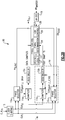
- FIG. 2A is a schematic diagram of one embodiment of a master clock and data recovery (CDR) circuit 20.
- the CDR circuit 20 includes a first or data sampler 11a, a second or edge sampler 11b, a first or data deserializer 12a, a second or edge deserializer 12b, a first phase selector 15a, a second phase selector 15b, a clock shaping circuit 16, a phase difference encoder 17, and a phase control circuit 18.
- the illustrated phase control circuit 18 includes voting logic 13 and an accumulator 14.
- the CDR circuit 20 receives an input data signal or stream D IN and an input clock signal CLK IN , and generates an output data signal D OUT and a master phase error signal ⁇ MASTER .
- the CDR circuit 20 illustrates one example of a master CDR circuit which can provide phase error forwarding to one or more slave CDR circuits.
- teachings herein are applicable to a wide variety of CDR circuits, including, for example, configurations using more or fewer blocks and/or a different arrangement of blocks.
- the illustrated CDR circuit 20 is implemented in a half-rate configuration using two samplers and two phase selectors.
- the first sampler 11a is configured to sample the input data stream D IN on both rising and falling edges of a data sampling clock signal CLK SAMPLE_DATA to generate data samples for the first deserializer 12a.
- the second sampler 11b is configured to sample the input data stream D IN on both rising and falling edges of an edge sampling clock signal CLK SAMPLE_EDGE to generate edge samples for the second deserializer 12b.
- the illustrated clock shaping circuit 16 receives an input clock signal CLK IN and generates an in-phase reference clock signal CLK I and a quadrature-phase reference clock signal CLK Q for the first and second phase selectors 15a, 15b.
- the clock shaping circuit 16 is illustrated as receiving one input clock signal and generating two reference clock signals, other configurations are possible, such as implementations in which the clock shaping circuit 16 receives additional input clock signals and/or generates more or fewer reference clock signals.
- the clock shaping circuit 16 is omitted in favor of providing one or more reference clock signals directly to clock generation circuitry used to generate data and edge sampling clock signals.
- the first phase selector 15a generates the data sampling clock signal CLK SAMPLE_DATA and the second phase selector 15b generates the edge sampling clock signal CLK SAMPLE_EDGE .
- the first and second phase selectors 15a, 15b can generate the data and edge sampling clock signals CLK SAMPLE_DATA , CLK SAMPLE_EDGE by interpolating the in-phase and quadrature-phase reference clock signals CLK I , CLK Q generated by the clock shaping circuit 16 based on a master phase signal ⁇ MASTER generated by the phase control circuit 18.
- the first and second phase selectors 15a, 15b can maintain a quadrature phase relationship between the data and edge phase sampling clock signals CLK SAMPLE_DATA , CLK SAMPLE_EDGE and can move the sampling clock signals in lock-step.
- the input data stream D IN can include a string of serial data bits that transition at a data rate. At a given data rate, the input data stream D IN has a unit interval (UI), or minimum time interval between transitions of the input data stream D IN .
- UI unit interval
- the samples can be taken from specific positions into the UI of the input data stream D IN .
- the samples taken by the data sampler 11a can include data samples taken from the middle of the UI
- the samples taken by the edge sampler 11b can include edge samples taken at the ends of the UI.
- the input data stream D IN received by the CDR circuit 20 can have a data rate of F DATA .
- the data output signal D OUT can correspond to a k-bit parallel data word having a data rate of F DATA / k .
- the CDR circuit 20 can operate as a deserializer.
- the data sampler 11a provides data samples to the first deserializer 12a
- the edge sampler 11b provides edge samples to the second deserializer 12b.
- the first and second deserializers 12a, 12b can be used to deserialize the data and edge samples, respectively.
- the first deserializer 12a provides the deserialized data samples to the data output terminal D OUT and to the voting logic 13 and the second deserializer 102b provides the deserialzed edge samples to the voting logic 13.
- the first and second deserializers 12a, 12b can provide the captured samples to the phase control circuit 18 at a reduced bit rate, thereby relaxing an operating frequency design constraint of the phase control circuit 18.
- the first and second deserializers 12a, 12b deserialize the data and edge samples streams by a factor of 8 or more.
- the phase control circuit 18 includes the voting logic 13 and the accumulator 14, which can be used to generate the master phase signal ⁇ MASTER .
- the master phase signal ⁇ MASTER is provided to the first phase selector 15a, which can use the master phase signal ⁇ MASTER to control timing of the data sampling clock signal CLK SAMPLE_DATA .
- the voting logic 13 can increase or decrease a value stored in the accumulator 14 to control the master phase signal ⁇ MASTER .
- the voting logic 13 can be used to process timing of data transitions between the edge and data samples so as to shift the data and edge sampling clock signals CLK SAMPLE_DATA , CLK SAMPLE_EDGE earlier or later in time to align the data and edge sampling clock signals CLK SAMPLE_DATA , CLK SAMPLE_EDGE relative to the UI of the input data stream D IN .
- the accumulator 14 is a digital wrapping accumulator.
- the first phase selector 15a can be used to generate the data sampling clock signal CLK SAMPLE_DATA based on the master phase signal ⁇ MASTER and the in-phase and quadrature-phase reference clock signals CLK I , CLK Q .
- the first phase selector 15a can be used to interpolate the in-phase reference clock signal CLK I and the quadrature-phase reference clock signal CLK Q to generate the data sampling clock signal CLK SAMPLE_DATA with a phase indicated by the master phase signal ⁇ MASTER .
- the phase control circuit 18 also generates a phase signal for the second phase selector 15b.
- the second phase selector 15b can interpolate the in-phase reference clock signal CLK I and the quadrature-phase reference clock signal CLK Q based on the phase signal.
- the phase signal provided to the second phase selector 15b can be, for example, the master phase signal ⁇ MASTER or a phase-shifted version thereof.
- the first and second phase selectors 15a, 15b have a similar circuit implementation as one another, and the master phase signal ⁇ MASTER provided to the first phase selector 15a and the phase signal provided to the second phase selector 15b can be about 90 degrees out of phase.
- the first and second phase selectors 15a, 15b have different circuit implementations and/or receive different reference clock signals, and both the first and second phase selectors 15a, 15b can receive the master phase signal ⁇ MASTER .
- the CDR circuit 20 includes an embedded delay-locked loop (DLL), which can be used to phase-lock the CDR circuit 20 to the input data stream D IN .
- the embedded DLL can include the first and second samplers 11a, 11b, the first and second deserializers 12a, 12b, the phase control circuit 18, and the first and second phase selectors 15a, 15b.
- the DLL operates to set a value of the master phase signal ⁇ MASTER to control sampling of the input data stream D IN .
- the master phase signal ⁇ MASTER can be adjusted to reduce or minimize individual bit errors of the k -bit output word generated by the CDR circuit 20 by controlling the alignment of the data and edge sampling clock signals CLK SAMPLE_DATA , CLK SAMPLE_EDGE relative to the UI of the input data stream D IN .
- the CDR circuit 20 also includes the phase difference encoder 17, which generates the master phase error signal ⁇ MASTER based on a change of the master phase signal ⁇ MASTER over time.
- the phase difference encoder 17 generates the master phase error signal ⁇ MASTER based on encoding a difference between the master phase signal ⁇ MASTER and a delayed version thereof.
- the master phase error signal ⁇ MASTER can be provided to one or more slave CDR circuits for phase error forwarding.
- FIG. 2B is a schematic diagram of one embodiment of a slave CDR circuit 30.
- the CDR circuit 30 includes the first and second samplers 11a, 11b, the first and second deserializers 12a, 12b, the first and second phase selectors 15a, 15b, and the clock shaping circuit 16, which can be as described earlier.
- the slave CDR circuit 30 further includes a phase difference decoder 19 and a phase control circuit 28 that includes voting logic 13, an accumulator 14, a phase determination circuit 24, and a CDR control circuit 25.
- the CDR circuit 30 illustrates one example of a slave CDR circuit which receives phase error information forwarded from a master CDR circuit, such as the master CDR circuit 20 of Figure 2A .
- a master CDR circuit such as the master CDR circuit 20 of Figure 2A .
- teachings herein are application to a wide variety of CDR circuits, including, for example, CDR circuits using more or fewer blocks and/or a different arrangement of blocks.
- the phase difference decoder 19 receives the master phase error signal ⁇ MASTER , and decodes the master phase error signal ⁇ MASTER to generate a decoded phase error signal PES.
- the phase control circuit 28 receives the decoded phase error signal PES and data and edge samples from the first and second deserializers 12a, 12b. As shown in Figure 2B , the phase control circuit 28 generates a slave phase signal ⁇ SLAVE , which is provided to the first phase selector 15a.
- the first phase selector 15a uses the slave phase signal ⁇ SLAVE to control a phase of the data sampling clock signal CLK SAMPLE_DATA used to capture the data samples from the input data stream D IN .
- phase control circuit 28 can generate the slave phase signal ⁇ SLAVE based on the decoded phase error signal PES. However, when the CDR circuit 30 is not operating using phase error forwarding, the phase control circuit 28 can generate the slave phase signal ⁇ SLAVE based on the data and edge samples generated by the first and second deserializers 12a, 12b.
- the phase control circuit 28 generates an edge tracking enable signal EN EDGE .
- the edge tracking enable signal EN EDGE is provided to edge tracking circuitry 26, which includes the edge sampler 11b, the edge deserializer 12b, and the second phase selector 15b.
- the edge tracking enable signal EN EDGE can be used to turn on or off all or part of the edge tracking circuitry 26 when the CDR circuit 30 is tracking the input data stream D IN based on the forwarded master phase error signal ⁇ MASTER .
- the edge tracking enable signal EN EDGE can be used to disable the edge tracking circuitry 26 to conserve power.
- the edge tracking circuitry 26 can remain turned on, and the voting logic 13 and the accumulator 14 can be used to generate a local phase signal used to control a value of the slave phase signal ⁇ SLAVE .
- the phase control circuit 28 also generates a phase signal for the second phase selector 15b.
- the phase signal provided to the second phase selector 15b can be, for example, the slave phase signal ⁇ SLAVE or a phase-shifted version thereof.
- the first and second phase selectors 15a, 15b have a similar circuit implementation as one another, and the slave phase signal ⁇ SLAVE provided to the first phase selector 15a and the phase signal provided to the second phase selector 15b are about 90 degrees out of phase.
- the first and second phase selectors 15a, 15b have different circuit implementations and/or receive different reference clock signals, and both the first and second phase selectors 15a, 15b receive the slave phase signal ⁇ SLAVE .
- the phase control circuit 28 can be used to process the decoded phase error signal PES to update the slave phase signal ⁇ SLAVE .
- the phase control circuit 28 includes the phase determination circuit 24 and the CDR control circuit 25, which can aid the phase control circuit 28 in processing the decoded phase error signal PES and in generating the slave phase signal ⁇ SLAVE .
- Various embodiments of the phase determination circuit 24 and the CDR control circuit 25 are described in detail further below with reference to Figures 5 , 7 , and 8 .
- FIG. 2C is a schematic diagram of one embodiment of a configurable master/slave CDR circuit 40.
- the CDR circuit 40 includes the first and second samplers 11a, 11b, the first and second deserializers 12a, 12b, the first and second phase selectors 15a, 15b, the clock shaping circuit 16, the phase difference encoder 17, and the phase difference decoder 19, which can be as described earlier.
- the CDR circuit 40 further includes a phase control circuit 38 that includes voting logic 13, the accumulator 14, the phase determination circuit 24, and the CDR control circuit 25.
- the CDR circuit 40 illustrates one example of a CDR circuit that can be configured in either a master mode or in a slave mode.
- the phase control circuit 38 receives a master/slave mode control signal, which can be used to control operation of the CDR circuit 40 as either a master CDR circuit or a slave CDR circuit.
- the phase difference encoder 17 can be used to generate the master phase error signal ⁇ MASTER , which can be forwarded to one or more slave CDR circuits.
- the phase difference decoder 19 can receive the master phase error signal ⁇ MASTER , which can be decoded to generate a decoded phase error signal PES for the phase control circuit 38.
- a CDR circuit that can be operated in either a master mode or a slave mode can enhance the flexibility of a chip-to-chip communication system.
- the chip-to-chip communication system can include two or more CDR circuits that are configurable in a master mode or a slave mode, and a particular CDR circuit can operate as master or slave depending on a particular application and/or operating environment of the chip-to-chip communication system.
- FIG 3 is a graph illustrating one example of a timing diagram 45 for a CDR circuit.
- the timing diagram 45 illustrates a configuration of a half-rate CDR circuit, and illustrates one example of possible timing of the CDR circuits of Figures 2A-2C .
- other configurations of timing are possible.
- the timing diagram 45 includes a first plot of an input data signal or stream D IN , a second plot of a data sampling clock signal CLK SAMPLE_DATA , and a third plot of an edge sampling clock signal CLK SAMPLE_EDGE .
- the timing diagram 45 has been annotated to illustrate sampling times of a first data sample 46a, a second data sample 46b, a first edge or transition sample 47a, and a second edge sample 47b.
- the timing diagram 45 has also been annotated to show a unit interval (UI) of the input data stream D IN .
- UI unit interval
- FIG 4A is a schematic diagram of a phase difference encoder 50 according to one embodiment.
- the phase difference encoder 50 includes a cycle delay circuit 51, a subtraction circuit 52, and an encoder 53.
- the illustrated phase difference encoder 50 receives a master phase signal ⁇ MASTER and a clock signal CLK and generates a master phase error signal ⁇ MASTER that is encoded.
- the cycle delay circuit 51 receives the clock signal CLK and the master phase signal ⁇ MASTER , and can generate a delayed master phase signal ⁇ DELAYED by delaying the master phase signal ⁇ MASTER by one or more cycles of the clock signal CLK. In certain configurations, the cycle delay circuit 51 generates the delayed master phase signal ⁇ DELAYED based on delaying the master phase signal ⁇ MASTER for two or more cycles of the clock signal CLK. However, other configurations are possible.
- Increasing a delay of the cycle delay circuit 51 can increase a time between updates or changes to the master phase error signal ⁇ MASTER , which can ease timing constraints in forwarding the master phase error signal ⁇ MASTER to one or more slave CDR circuits.
- delaying the master phase signal ⁇ MASTER by a relatively large number of cycles may also degrade the slave CDR circuits' ability to maintain lock in the presence of large amounts of jitter.
- the subtraction circuit 52 includes a first input that receives the master phase signal ⁇ MASTER , a second input that receives the delayed master phase signal ⁇ DELAYED , and an output that generates a phase difference signal corresponding to a difference between the master phase signal ⁇ MASTER and the delayed master phase signal ⁇ DELAYED .
- the encoder 53 receives the phase difference signal and the clock signal CLK, and can encode the phase difference signal to generate the master phase error signal ⁇ MASTER .
- the master phase error signal ⁇ MASTER can be provided to one or more slave CDR circuits and can be used for phase error forwarding.
- FIG 4B is a schematic diagram of a phase difference decoder 60 according to one embodiment.
- the phase difference decoder 60 includes a decoder 61 and a phase difference interpolator 62.
- the phase difference decoder 60 receives a clock signal CLK and the master phase error signal ⁇ MASTER , which can be generated by the phase difference encoder 50 of Figure 4A .
- the phase difference decoder 60 generates a decoded phase error signal PES that can be used to adjust a slave phase signal in a slave CDR circuit.
- the decoder 61 receives the clock signal CLK and the master phase error signal ⁇ MASTER , and can decode the master phase error signal ⁇ MASTER to generate a decoded master phase difference signal for the phase difference interpolator 62.
- the phase difference interpolator 62 receives the decoded master phase difference signal and the clock signal CLK, and can generate the decoded phase error signal PES by interpolating the decoded master phase difference signal over two or more cycles of the clock signal CLK, such as by a number of cycles of delay provided by the cycle delay circuit 51 of Figure 4A .
- the phase difference interpolator 62 can generate the decoded phase error signal PES based on interpolating the decoded master phase difference signal over k cycles.
- changes to a slave phase signal of a slave CDR circuit can occur more gradually relative to a configuration in which the decoded phase error signal PES is incremented or decremented only once every k cycles.
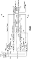
- FIG. 5 is a schematic diagram of a CDR sub-circuit 70 according to one embodiment.
- the illustrated CDR sub-circuit 70 includes a phase difference decoder 78, a phase determination circuit 71, and a CDR control circuit 72.
- the CDR sub-circuit 70 can represent a portion of a CDR circuit.
- the phase determination circuit 71 and the CDR control circuit 72 can be included in a phase control circuit, such as the phase control circuit 28 of Figure 2B or the phase control circuit 38 of Figure 2C .
- the phase difference decoder 78 illustrates one implementation of a phase difference decoder, such as the phase difference decoder 19 of Figures 2B and 2C .
- the phase difference decoder 78 receives the master phase error signal ⁇ MASTER and a phase offset signal ⁇ OFFSET . Additionally, the phase difference decoder 78 generates a decoded phase error signal PES, which is provided to the phase determination circuit 71.
- the illustrated phase determination circuit 71 includes an adder 81, a first selection circuit 82, registers 83, and a second selection circuit 84.
- the adder 81 can be used to add a stored phase signal ⁇ STORED from the registers 83 and the decoded phase error signal PES to generate a forwarded phase signal ⁇ FWD .
- the first selection circuit 82 can be used to select between the forwarded phase signal ⁇ FWD and a local phase signal ⁇ LOCAL as an input to the registers 83.
- the local phase signal ⁇ LOCAL can be generated by, for example, an accumulator of a slave CDR circuit when the slave CDR circuit is operating without phase error forwarding.
- the second selection circuit 84 can be used to generate the slave phase signal ⁇ SLAVE by selecting between the stored phase signal ⁇ STORED and the local phase signal ⁇ LOCAL .
- the slave phase signal ⁇ SLAVE can be used to control a phase of a data sampling clock signal used to capture data samples from an input data stream received by the slave CDR circuit.
- the registers 83 can be used to store a sum of the forwarded phase signal ⁇ FWD and the decoded phase error signal PES.
- the second selection circuit 84 selects the stored phase signal ⁇ STORED
- the slave phase signal ⁇ SLAVE can correspond to the stored phase signal ⁇ STORED .
- the slave phase signal ⁇ SLAVE can be generated using phase error forwarding, and the slave phase signal ⁇ SLAVE can track master phase information via changes to the decoded phase error signal PES.
- the registers 83 can be used to store the local phase signal ⁇ LOCAL .
- the slave phase signal ⁇ SLAVE can correspond to the local phase signal ⁇ LOCAL .
- the slave phase signal ⁇ SLAVE can be generated using phase information local to the slave CDR circuit.
- the illustrated CDR control circuit 72 includes a jitter coherence detection circuit 91, a phase error forwarding control circuit 92, an offset correction circuit 93, and a token handling circuit 94.
- the jitter coherence detection circuit 91 receives the local phase signal ⁇ LOCAL and the forwarded phase signal ⁇ FWD , and provides a jitter coherence signal to the phase error forwarding control circuit 92.
- the phase error forwarding control circuit 92 receives a system enable EN SYS and generates an edge tracking enable signal EN EDGE .
- the phase error forwarding control circuit 92 also controls the selections of the first and second selection circuits 82, 84, and can send or receive one or more signals to or from the jitter coherence detection circuit 91, the offset correction circuit 93, and/or the token handling circuit 94 to provide control over clock and data recovery operations.
- the offset correction circuit 93 receives the local phase signal ⁇ LOCAL and the forwarded phase signal ⁇ FWD , and generates a phase offset signal ⁇ OFFSET , which is provided to the phase difference decoder 78 in the illustrated configuration.
- the token handling circuit 94 can send or receive a token TOKEN over a token handling interface.
- the jitter coherence detection circuit 91 can generate a jitter coherency signal that indicates whether or not jitter between a first input data stream received by a master CDR circuit and a second input data stream received by a slave CDR circuit is coherent.
- jitter coherency is determined in part by tracking incoming data in the master CDR circuit and the slave CDR circuit separately, and observing a difference between the local phase signal ⁇ LOCAL and the forwarded phase signal ⁇ FWD .
- the jitter between the data streams is not coherent, it may unreliable to use phase error forwarding.
- the phase error forwarding control circuit 92 can turn on the slave CDR circuit's local edge tracking circuitry, and control the second phase selection circuit 84 to generate the slave phase signal ⁇ SLAVE using the local phase signal ⁇ LOCAL .
- the jitter coherence detection circuit 91 should not inhibit the phase error forwarding control circuit 92 from using phase error forwarding.
- the offset correction circuit 93 can be used to generate the phase offset signal ⁇ OFFSET , which can indicate a phase offset of a slave phase signal (for example, ⁇ SLAVE of Figure 2B ) of a slave CDR circuit relative to a master phase signal (for example, ⁇ MASTER of Figure 2A ) of a master CDR circuit.
- a chip-to-chip communication system includes two or more slave CDR circuits, and each of the slave CDR circuits can have different phase offsets relative to one another.
- the phase offset ⁇ OFFSET can be separately set for each slave CDR circuit to enhance tracking and/or to reduce output bit errors.
- the phase offset signal ⁇ OFFSET can be generated in a variety of ways, such as by tracking incoming data in a master CDR circuit and a slave CDR circuit over several clock cycles, and observing a difference between the forwarded phase signal ⁇ FWD and the local phase signal ⁇ LOCAL .
- the phase offset signal ⁇ OFFSET corresponds to an average observed difference between the forwarded phase signal ⁇ FWD and the local phase signal ⁇ LOCAL over an observation interval.
- a slave CDR circuit can operate using phase error forwarding, but the phase offset signal ⁇ OFFSET may be regularly calibrated or updated. Configuring the slave CDR circuit in this manner can enhance the robustness of phase error forwarding, and can be used to compensate for a phase drift between the master CDR circuit and the slave CDR circuit over time.
- the phase offset ⁇ OFFSET is determined during an interval of time in which the slave CDR circuit holds a token received over a token handling interface.
- the CDR control circuit 72 includes the token handling circuit 94, which can aid the CDR circuit in receiving and passing the token over the token handling interface.
- the token handling circuit 94 can communicate with the phase error forwarding control circuit 92. When the token is received, the phase offset ⁇ OFFSET can be updated.
- phase offset ⁇ OFFSET is provided to the phase difference decoder 78, which can interpolate the phase offset ⁇ OFFSET over multiple clock cycles.
- phase difference decoder 78 can interpolate the phase offset ⁇ OFFSET over multiple clock cycles.
- other configurations are possible, such as implementations in which the phase offset ⁇ OFFSET is directly added to the forwarded phase signal ⁇ FWD .
- FIG 6 is a flow diagram of a method 150 of clock and data recovery according to one embodiment.
- the method 150 can be used for recovering data in a chip-to-chip communication system, such as the chip-to-chip communication system 10 of Figure 1 . It will be understood that the method may include greater or fewer operations.
- the illustrated method 150 of clock and data recovery starts at block 151, in which a CDR system including a master CDR circuit and a slave CDR circuit is initialized.
- the CDR system can include additional slave CDR circuits.
- the CDR system can be, for example, a chip-to-chip communication system.
- the master and slave CDR circuits can wait for ancillary blocks to power-up and/or complete any initialization procedures. For instance, the master and slave CDR circuits can wait for one or more PLLs to lock and/or for any adaptive equalizers to initialize.
- the method 150 continues at a block 152, in which incoming data is tracked using the master CDR circuit and the slave CDR circuit using separate phase information. Thus, in block 152, phase error forwarding is not used.
- the jitter coherence of the master CDR circuit and the slave CDR circuit is compared. Once both the master CDR circuit and the slave CDR circuit are tracking their own respective input data streams, the slave CDR circuit can continue to track its input data stream while comparing local phase information to the phase information forwarded by the master. Configuring the slave CDR circuit in this manner can aid in assessing a coherence of jitter between the master CDR circuit and the slave CDR circuit.
- the method 150 continues at a decision block 154 in which it is determined if the jitter is coherent or incoherent.
- the jitter coherence of the master CDR circuit and the slave CDR circuit can be compared in a variety of ways.
- the slave CDR circuit determines a phase difference between local phase information and the phase information forwarded by the master, and compares the phase difference to a threshold phase or phase tolerance. Additionally, when the phase difference is determined to be less than the threshold phase, the jitter is determined to be coherent. However, when the phase difference is greater than or equal to the threshold phase, the jitter is determined to be incoherent.
- the method returns to block 152, in which the incoming data is tracked in the master CDR circuit and the slave CDR circuit using separate phase information.
- the slave CDR circuit may continue to track incoming data using separate phase information.
- the method continues at a block 155, in which the initial phase or phase offset of the slave CDR circuit is adjusted.
- the slave CDR circuit should have an appropriate initial phase offset relative to the master CDR circuit.
- the initial phase of the slave CDR circuit can be adjusted or calibrated to determine the phase offset between the slave CDR circuit and the master CDR circuit.
- the phase offset can be used to enhance the accuracy of phase error forwarding and/or to reduce bit errors in an output data signal generated by the slave CDR circuit.
- the initial phase can be adjusted to calibrate out a residual phase difference between the master CDR circuit and the slave CDR circuit by averaging an error between a forwarded phase and a local phase over an observation interval.
- the slave CDR circuit follows the master phase information. To conserve power, certain circuitry of the slave CDR circuit, such as edge tracking circuitry and/or DLL control circuitry can be turned off to reduce power consumption.
- the master CDR circuit generates an encoded phase difference signal representing a change to the master's phase signal over two or more clock cycles.
- the encoded phase difference signal can be forwarded to the slave CDR circuit, and decoded and interpolated over the two or more clock cycles to generate a decoded phase error signal the can be used to adjust the slave CDR circuit's local phase signal.
- the method 150 continues at a decision block 157, in which the slave CDR circuit determines if a timeout has been reached.
- the slave CDR circuit may follow the master phase information until timeout.
- the duration of the timeout can be determined in a variety of ways, such as by a particular number of clock cycles. However, other configurations are possible.
- the method returns to block 156, in which the slave CDR circuit follows the master phase information.
- the method 150 continues to a block 158, in which slave CDR circuit waits for a token.
- the slave CDR circuit may be one of several slave CDR circuits that operate using phase information forwarded by the master CDR circuit. However, when there are multiple slave CDR circuits, it may be advantageous to calibrate less than all of the slave CDR circuits at a time. Configuring the slave CDR circuits in this manner can reduce a magnitude of a power supply perturbation associated with calibration.
- the slave CDR circuits may use a token passing scheme to periodically calibrate the phase offset of the slave CDR circuits, while avoiding power glitches and/or surges associated with powering the edge tracking circuitry of two or more of the slave CDR circuits simultaneously.
- the method 150 continues at a decision block 159, in which the slave CDR circuit determines if a slave enable token is available.
- the method returns to block 158, in which the slave CDR circuit waits for the token.
- the method continues at a block 160, in which the master CDR circuit and the slave CDR circuit track incoming data using separate phase information.
- the method 150 returns to block 155, in which the initial phase of the slave CDR circuit is adjusted. In the block 155, the phase offset of the slave CDR circuit can be calibrated.
- a slave CDR circuit can intermittently turn on its own edge tracking and DLL circuitry to ensure that the slave CDR circuit is following a correct phase associated with its own input data stream.
- the slave CDR circuit can release the token. Accordingly, in certain configurations, the slave CDR circuit can release the token after adjusting the initial phase of the slave CDR circuit in block 155.
- a slave CDR circuit can operate in a tracking mode whereby the slave CDR circuit follows the master CDR circuit's phase information indefinitely.
- FIG. 7 is a schematic diagram of a CDR sub-circuit 170 according to another embodiment.
- the illustrated CDR sub-circuit 170 includes a phase difference decoder 178, a phase determination circuit 171, and a CDR control circuit 172.
- the CDR sub-circuit 170 can represent a portion of a CDR circuit.
- the phase determination circuit 171 and the CDR control circuit 172 can be included in a phase control circuit, such as the phase control circuit 28 of Figure 2B or the phase control circuit 38 of Figure 2C .
- the phase difference decoder 178 illustrates one implementation of a phase difference decoder, such as the phase difference decoder 19 of Figures 2B and 2C .
- the phase difference decoder 178 receives the master phase error signal ⁇ MASTER and a clock signal CLK. Additionally, the phase difference decoder 178 generates a decoded phase error signal PES, which is provided to the phase determination circuit 171.
- the master phase error signal ⁇ MASTER comprises m bits
- the decoded phase error signal PES comprises n bits. In one embodiment, m is selected to be in the range of 2 bits to 4 bits, and n is selected to be in the range of 2 bits to 3 bits. However, other implementations are possible.
- the illustrated phase determination circuit 171 includes an adder 181, a first multiplexer 182, flip-flops 183, and a second multiplexer 184.
- the adder 181 can be used to add a stored phase signal ⁇ STORED from the flip-flops 183 and the decoded phase error signal PES to generate a forwarded phase signal ⁇ FWD .
- the first multiplexer 182 can be used to select between the forwarded phase signal ⁇ FWD and a local phase signal ⁇ LOCAL as an input to the flip-flops 183.
- the second multiplexer 184 can be used to generate the slave phase signal ⁇ SLAVE by selecting between the stored phase signal ⁇ STORED and the local phase signal ⁇ LOCAL .
- the stored phase signal ⁇ STORED , the forwarded phase signal ⁇ FWD , the local phase signal ⁇ LOCAL , and the slave phase signal ⁇ SLAVE each comprise n bits.
- the illustrated CDR control circuit 172 includes a jitter coherence detection circuit 191 and a phase error forwarding control circuit 192.
- the jitter coherence detection circuit 191 receives the local phase signal ⁇ LOCAL , the forwarded phase signal ⁇ FWD , a tolerance signal TOLERANCE, and the clock signal CLK, and provides a jitter coherence signal to the phase error forwarding control circuit 192.
- the phase error forwarding control circuit 192 controls the selections of the first and second multiplexers 182, 184, and can send or receive one or more signals to or from the jitter coherence detection circuit 191.
- the jitter coherence detection circuit 191 can be used to determine whether or not jitter between a first input data stream received by a master CDR circuit and a second input data stream received by a slave CDR circuit is coherent.
- the jitter coherency is determined by tracking incoming data in the master CDR circuit and the slave CDR circuit separately, and observing an average phase difference between the local phase signal ⁇ LOCAL and the forwarded phase signal ⁇ FWD over q cycles of the clock signal CLK.
- the jitter coherence detection circuit 191 can generate the jitter coherence signal by comparing the average phase difference to the tolerance signal TOLERANCE. For example, when the average phase difference is greater than the tolerance signal TOLERANCE, the jitter can be determined to be incoherent.
- q is selected to be in the range of 1,024 clock cycles to 33,554,432 clock cycles.
- CDR sub-circuit 170 Additional details of the CDR sub-circuit 170 can be similar to those described earlier.
- FIG 8 is a schematic diagram of a CDR sub-circuit 200 according to one embodiment.
- the illustrated CDR sub-circuit 200 includes a phase difference decoder 208, a phase determination circuit 171, and a CDR control circuit 202.
- the CDR sub-circuit 200 can represent a portion of a CDR circuit.
- the phase determination circuit 171 and the CDR control circuit 202 can be included in a phase control circuit, such as the phase control circuit 28 of Figure 2B or the phase control circuit 38 of Figure 2C .
- the phase difference decoder 208 illustrates one implementation of a phase difference decoder, such as the phase difference decoder 19 of Figures 2B-2C .
- the phase difference decoder 208 receives the master phase error signal ⁇ MASTER , a clock signal CLK, and a phase offset signal ⁇ OFFSET . Additionally, the phase difference decoder provides a decoded phase error signal PES to the phase determination circuit 171, which can be as described earlier.
- the phase offset signal ⁇ OFFSET comprises l bits. In one embodiment, l is selected to be in the range of 3 bits to 4 bits. However, other implementations are possible.
- the illustrated CDR control circuit 202 includes a phase error forwarding control circuit 212 and an offset correction circuit 213.
- the phase error forwarding control circuit 212 receives the clock signal CLK, and generates selection control signals for controlling selections of the first and second multiplexers 182, 184.
- the phase error forwarding control circuit 212 further generates an enable signal and a reset signal RESET, which can be used in part by the offset correction circuit 213 to generate the phase offset signal ⁇ OFFSET , as will be described below.
- the offset correction circuit 213 receives the clock signal CLK, the local phase signal ⁇ LOCAL , the forwarded phase signal ⁇ FWD , the enable signal, the reset signal RESET, and generates the phase offset signal ⁇ OFFSET .
- the offset correction circuit 213 includes a subtractor 221, an adder 222, a first group of flip-flops 223, a phase averaging circuit 224, and a second group of flip-flops 225.
- the subtractor 221 can be used to generate an n -bit difference signal based on a difference between the local phase signal ⁇ LOCAL and the forwarded phase signal ⁇ FWD .
- the n -bit difference signal can be added to a p -bit output signal from the first group of flip-flops 223, and provided as a p -bit input signal to the first group of flip-flops 223.
- the p -bit output signal from the first group of flip-flops 223 can be averaged by the phase averaging circuit 224 to generate the phase offset ⁇ OFFSET .
- the p is selected to be in the range of 13 bits to 14 bits. However, other implementations are possible.
- the phase error forwarding control circuit 212 can initially use the reset signal RESET to reset a state of the first group of flip-flops 223 and the p -bit output signal. Thereafter, the first group of flip-flops 223 can be used to accumulate or integrate a difference between the local phase signal ⁇ LOCAL and the forwarded phase signal ⁇ FWD over r cycles of the clock signal CLK. Additionally, the phase averaging circuit 224 can be used to divide the p -bit output signal from the first group of flip-flops 223 by the r cycles to generate an l -bit input signal to second group of flip-flops 225.
- second group of flip-flops 225 can control a value of the phase offset ⁇ OFFSET based on the l -bit input signal generated by the phase averaging circuit 224.
- r is selected to be in the range of 1024clock cycles to 2048 clock cycles
- l is selected to be in the range of 3 bits to 4 bits.
- other configurations are possible.
- FIG. 9 is a schematic diagram of an electronic system 300 that includes CDR circuits using token passing according to one embodiment.
- the illustrated electronic system 300 includes a first CDR circuit 307a, a second CDR circuit 307b, and a third CDR circuit 307c. Although illustrated as including three CDR circuits, the electronic system 300 can be adapted to include more or fewer CDR circuits.
- the first CDR circuit 307a includes a first token handling circuit 308a. Additionally, the second CDR circuit 307b includes a second token handling circuit 308b, and the third CDR circuit 307c includes a third token handling circuit 308c.
- the first token handling circuit 308a includes a token input T IN electrically connected to a token output T OUT of the second token handling circuit 308b.
- the second token handling circuit 308b includes a token input T IN electrically connected to a token output T OUT of the third token handling circuit 308c
- the third token handling circuit 308c includes a token input T IN electrically connected to a token output T OUT of the first token handling circuit 308a.
- the token inputs and outputs of the token handling circuits 308a-308c are electrically connected in a ring that can be used to pass a token.
- the first token handling circuit 308a further includes a first feedback input F IN electrically connected to a feedback output F OUT of the third token handling circuit 308c.
- the second token handling circuit 308b includes a feedback input F IN electrically connected to a feedback output F OUT of the first token handling circuit 308a
- the third token handling circuit 308c includes a feedback input F IN electrically connected to a feedback output F OUT of the second token handling circuit 308b.
- the feedback information provided can include, for example, information indicating whether or not the CDR circuit is ready to accept the token and/or information whether a slave further up the chain has taken the token for themselves.
- the illustrated token handling circuits 308a-308c each generate a token requested signal (TOKEN REQUESTED) and a token granted signal (TOKEN GRANTED).
- a token handling control circuit can be included in a CDR control circuit (for example, the CDR control circuit 72 of Figure 5 ), and the token requested and token received signals can be associated with communications between the token handling circuit and the CDR control circuit's phase error forwarding control circuit (for example, the phase error forwarding control circuit 92 of Figure 5 ).
- the token is passed in a first or clockwise direction, and feedback information is communicated in a second or counterclockwise direction.
- feedback information is communicated in a second or counterclockwise direction.
- other configurations are possible, such as implementations in which the token is passed in a counterclockwise direction and feedback information is communicated in a clockwise direction, or implementations including directions that are configurable or selectable.
- the CDR circuit can provide separate phase tracking independent of phase error forwarded from a master CDR circuit.
- the CDR circuit holding the token can have edge sampling circuitry and DLL circuitry turned on and used to track the CDR circuit's input data stream.
- the electronic system 300 can avoid power supply perturbations associated with activating several slave CDR circuits simultaneously.
- the token passing scheme can be used to ensure that one slave CDR circuit turns on at a time.
- the first CDR circuit 307a, the second CDR circuit 307b, and the third CDR circuit 307c operate as slave CDR circuits that receive a master phase error signal from a master CDR circuit that is not shown.
- the first, second, and third CDR circuits 307a-307c can be individually configurable between a master mode and a slave mode.
- the CDR circuit's token handling circuit can be configured to pass feedback information from an upstream CDR circuit to a downstream CDR circuit and to pass a token from the downstream CDR circuit to the upstream CDR circuit.
- a CDR circuit operated in the master mode should not hold the token.
- FIG 10A is a schematic diagram of a phase difference encoder 350 according to another embodiment.
- the phase difference encoder 350 includes a cycle delay circuit 351, a subtractor 352, and an encoder 353.
- the illustrated phase difference encoder 350 receives a master phase signal ⁇ MASTER and a clock signal CLK and generates a master phase error signal ⁇ MASTER that is encoded.
- the master phase signal ⁇ MASTER comprises 6 bits and the master phase error signal ⁇ MASTER comprises 4 bits.
- other configurations are possible.
- the cycle delay circuit 351 includes a first group of flip-flops 361 and a second group of flip-flops 362.
- the first and second groups of flip-flops can be used to generated a delayed master phase signal by delayed the master phase signal ⁇ MASTER by two cycles of the clock signal CLK.
- the subtractor 352 can generate a phase difference signal based on a difference between the master phase signal ⁇ MASTER and the delayed master phase signal generated by the cycle delay circuit 351.
- the phase difference signal corresponds to a change of the master phase signal ⁇ MASTER between two cycles of the clock signal CLK, and can indicate a change of master phase information over time.
- the encoder 353 includes a phase calculation circuit 371, exclusive or (XOR) gates 372, output flip-flops 373, an inverter 374, and an output enable control flip-flop 375.
- the phase calculation circuit 371 receives the phase difference signal from the subtractor 352, and generates an encoded signal that is provided as a first input to XOR gates 372.
- the encoded signal is generated using one-hot-plus-zero encoding.
- the encoded signal has 4 bits, and can have a value corresponding to one of the four possible one-hot states (b1000, b0100, b0010, b0001) or to the all-zero state (b0000).
- Using one-hot-plus-zero encoding can limit a maximum number of binary "1" values in the encoded signal to one, which permits a phase change to be indicated by an exclusive or operation between the encoded signal and a delayed version thereof.
- Figure 10A illustrates one possible code assignment for one-hot-plus-zero encoding of changes to the master phase signal ⁇ MASTER , in which a phase step decrease of two code values is assigned b1000, a phase step decrease of one code value is assigned b0100, no change to the phase step is assigned b0000, a phase step increase of one code value is assigned b0010, and a phase step increase of two code values is assigned b0001.
- other code assignments are possible.
- the XOR gates 372 further receive the master phase error signal ⁇ MASTER as a second input, and generate an XOR signal that as provided as an input to the output flip-flops 373.
- the output flip-flops 373 receive the clock signal CLK and an enable signal, and generate the master phase error signal ⁇ MASTER .
- the output flip-flops 373 can update or change the value of the master phase error signal ⁇ MASTER during cycles of the clock signal CLK in which the enable signal is logically high.
- the enable signal is generated by the inverter 374 and the enable control flip-flop 375, which are electrically connected in an inverting digital feedback loop.
- the input of the enable control flip-flop 375 is electrically connected to an output of the inverter 374 and the output of the enable control flip-flop 375 is electrically connected to an input of the inverter 374.
- the inverting digital feedback can result in the enable signal generated by the output flip-flops 373 toggling each cycle of the clock signal CLK, thereby resulting in the master phase error signal ⁇ MASTER changing once every other clock cycle.
- the illustrated phase difference encoder 350 encodes the master phase error signal ⁇ MASTER to indicate a change to the master phase information between two clock cycles.
- the phase difference encoder 350 encodes the master phase error signal ⁇ MASTER such that at most one bit of the master phase error signal ⁇ MASTER changes at a time. Encoding the master phase error signal ⁇ MASTER in this manner can reduce a number of decoding errors or an impact of decoding errors on operation of a slave CDR circuit that receives the master phase error signal ⁇ MASTER .
- the slave CDR circuit can include latches or flip-flops that sample the master phase error signal ⁇ MASTER , and encoding the master phase error signal ⁇ MASTER such that at most one bit is updated at a time can enhance robustness to metastability errors associated with sampling the master phase error signal ⁇ MASTER near bit transitions or changes.
- the clock signal CLK can have any suitable frequency, such as a frequency selected based on a rate of an input data stream received by a CDR circuit.
- the clock signal CLK has a frequency selected to be about F DATA / N , where F DATA is the data rate of the input data stream and N is a factor selected to be in the range of 20 to 40.
- F DATA is the data rate of the input data stream
- N is a factor selected to be in the range of 20 to 40.
- other clock signal frequencies are possible.
- the master phase error signal ⁇ MASTER can change up to once every other cycle.
- certain high frequency changes to the master phase signal ⁇ MASTER may be filtered by the phase difference encoder 350.
- the phase difference encoder 350 can filter changes to the master phase signal ⁇ MASTER associated with a limit cycle oscillation of a master CDR circuit.
- any slave CDR circuits operating using phase error forwarding may operate with no limit cycle oscillations or with limit cycle oscillations of smaller magnitude.
- a net step change of the master phase signal ⁇ MASTER can be two steps and the master phase error signal ⁇ MASTER can indicate a phase change of two steps.
- the phase difference encoder 350 can accumulate changes to the master phase error signal ⁇ MASTER that occur in the same direction.
- FIG 10B is a schematic diagram of a phase difference decoder 380 according to another embodiment.
- the phase difference decoder 380 includes a decoder 381 and a phase difference interpolator 382.
- the phase difference decoder 380 receives the clock signal CLK, the phase offset signal ⁇ OFFSET , and the master phase error signal ⁇ MASTER , and generates a decoded phase error signal PES.
- the phase offset signal ⁇ OFFSET can be generated by an offset correction circuit of a CDR control circuit.
- the master phase error signal ⁇ MASTER can be generated by a phase difference encoder, such as the phase difference encoder 350 of Figure 10A .
- the master phase error signal ⁇ MASTER comprises 4 bits
- the phase offset signal ⁇ OFFSET comprises 4 bits
- the decoded phase error signal PES comprises 2 bits.
- other configurations are possible.
- the decoder 381 receives the clock signal CLK and the master phase error signal ⁇ MASTER , and can decode the master phase error signal ⁇ MASTER to generate a decoded master phase difference signal for the phase difference interpolator 382.
- the decoder 381 includes a first group of flip-flops 391, a second group of flip-flops 392, XOR gates 393, and a phase calculation circuit 394.
- the first group of flip-flops 391 can delay the master phase error signal ⁇ MASTER by one cycle of the clock signal CLK
- the second group of flip-flops 392 can delay the master phase error signal ⁇ MASTER by an additional cycle of the clock signal CLK.
- the XOR gates 393 can generate an XOR signal based on an exclusive or operation of the outputs of the first and second groups of flip-flops 391, 392.
- the XOR signal can correspond to an exclusive or of the master phase error signal ⁇ MASTER and a version of the master phase error signal ⁇ MASTER delayed by one clock cycle.
- the phase calculation circuit 394 can receive the XOR signal, and can decode the XOR signal to generate a decoded phase difference signal for the phase difference interpolator 382.
- the phase calculation circuit 394 can provide a decoding that is complementary to an encoding provided by the phase calculation circuit 371 of Figure 10A .
- the decoded phase difference signal generated by the phase calculation circuit 394 indicates a phase step decrease of two code values when the XOR signal has value b1000, indicates a phase step decrease of one code value when the XOR signal has value b0100, indicates no change to the phase step when the XOR signal has value b0000, indicates a phase step increase of one code value when the XOR signal has value b0010, and indicates a phase step increase of two code values when the XOR signal has value b0001.
- other code assignments are possible.
- the phase difference interpolator 382 receives the decoded master phase difference signal, the phase offset signal ⁇ OFFSET , and the clock signal CLK, and can generate the decoded phase error signal PES by interpolating the decoded master phase difference signal and the phase offset signal ⁇ OFFSET over multiple cycles of the clock signal CLK.
- changes to the slave phase signal of a slave CDR circuit can occur more gradually relative to a configuration without interpolation.
- the slave CDR circuit can exhibit an enhanced ability to maintain phase-lock in the presence of jitter.
- the phase difference interpolator 382 includes a first adder 401, a second adder 402, flip-flops 403, a digital comparator 404, and a subtractor 405.
- the flip-flops 403 can store a residual phase difference signal corresponding to a phase difference to be interpolated by the phase difference interpolator 382 over multiple clock cycles.
- the digital comparator 404 can be used to determine whether the residual phase difference signal is greater than zero, less than zero, or equal to zero. Additionally, the decoded phase error signal PES can have a value of +1 when the residual phase difference signal is greater than zero, a value of 0 when the residual phase difference signal is equal to zero, and a value of -1 when the residual phase difference signal is less than zero.
- the subtractor 405 can subtract the decoded phase error signal PES from the residual phase difference signal, which can be added to the phase offset signal ⁇ OFFSET using the second adder 402.
- the phase offset signal ⁇ OFFSET can be provided after a calibration cycle, and can be set to a digital value of 0 thereafter.
- the first adder 401 adds the output of the second adder 402 to the decoded master phase difference signal generated by the decoder 381.
- the output of the first adder 401 is provided as an input to the flip-flops 403.
- the phase difference interpolator 382 includes a digital feedback loop that controls the decoded phase error signal PES based on an error signal corresponding to the residual phase difference signal stored in the flip-flops 403. Via digital feedback, the value of the decoded phase error signal PES can be controlled on a cycle-by-cycle basis to interpolate the residual phase difference signal across multiple clock cycles.
- Examples of the electronic devices can include, but are not limited to, medical imaging and monitoring, consumer electronic products, parts of the consumer electronic products, electronic test equipment, etc. Examples of the electronic devices can also include memory chips, memory modules, circuits of optical networks or other communication networks, and disk driver circuits.
- the consumer electronic products can include, but are not limited to, a mobile phone, a telephone, a television, a computer monitor, a computer, a hand-held computer, a personal digital assistant (PDA), a microwave, a refrigerator, an automobile, a stereo system, a cassette recorder or player, a DVD player, a CD player, a VCR, an MP3 player, a radio, a camcorder, a camera, a digital camera, a portable memory chip, a washer, a dryer, a washer/dryer, a copier, a facsimile machine, a scanner, a multifunctional peripheral device, a wrist watch, a clock, etc. Further, the electronic device can include unfinished products.
- PDA personal digital assistant
Landscapes
- Engineering & Computer Science (AREA)
- Computer Networks & Wireless Communication (AREA)
- Signal Processing (AREA)
- Theoretical Computer Science (AREA)
- General Engineering & Computer Science (AREA)
- Power Engineering (AREA)
- Physics & Mathematics (AREA)
- General Physics & Mathematics (AREA)
- Computer Hardware Design (AREA)
- Synchronisation In Digital Transmission Systems (AREA)
Claims (23)
- Takt- und Datenrückgewinnungssystem (CDR- Clock and Data Recovery), Folgendes umfassend:eine erste CDR-Schaltung (7a, 20), dafür konfiguriert, einen ersten Eingabedatenstrom (9a) zu empfangen und basierend auf dem Verfolgen des ersten Eingabedatenstroms ein Master-Phasen-Signal zu erzeugen, wobei die erste CDR-Schaltung ferner dafür konfiguriert ist, basierend auf einer Änderung des Master-Phasen-Signals im Zeitverlauf ein Master-Phasen-Fehlersignal (ΔΦmaster) zu erzeugen, undeine zweite CDR-Schaltung (7b, 7c, 30), dafür konfiguriert, das Master-Phasen-Fehlersignal (ΔΦmaster) von der ersten CDR-Schaltung (7a, 20) und einen zweiten Eingabedatenstrom (9b) zu empfangen, wobei die zweite CDR-Schaltung in einem ersten Modus ferner dafür konfiguriert ist, basierend auf dem Master-Phasen-Fehlersignal ein erstes Slave-Phasen-Signal zu erzeugen und den zweiten Eingabedatenstrom basierend auf dem ersten Slave-Phasen-Signal zu verfolgen,dadurch gekennzeichnet, dass die zweite CDR-Schaltung (7b) eine Randverfolgungsschaltung (26) umfasst und in einem zweiten Modus funktionsfähig ist, die Randverfolgungsschaltung (26) zu verwenden, um basierend auf dem Verfolgen des zweiten Eingabedatenstroms ein zweites CDR-Phasen-Signal zu erzeugen, wobei die zweite CDR-Schaltung dafür konfiguriert ist, mindestens einen Teil der Randverfolgungsschaltung abzuschalten, wenn die zweite CDR-Schaltung den zweiten Eingabedatenstrom mit Hilfe des Master-Phasen-Fehlersignals verfolgt, undwobei die erste CDR-Schaltung ferner einen Phasendifferenzcodierer (17) umfasst, der dafür konfiguriert ist, durch Codieren einer Differenz zwischen dem Master-Phasen-Signal und einer verzögerten Version des Master-Phasen-Signals das Master-Phasen-Fehlersignal zu erzeugen.
- CDR-System nach Anspruch 1, wobei das Master-Phasen-Fehlersignal mehrere Bits trägt, wobei der Phasendifferenzcodierer das Master-Phasen-Fehlersignal derart codiert, dass sich höchstens ein Bit der mehreren Bits auf einmal ändert.
- CDR-System nach Anspruch 1 oder 2, wobei der Phasendifferenzcodierer Folgendes umfasst:eine Zyklusverzögerungsschaltung (51), die dafür konfiguriert ist, durch Verzögern des Master-Phasen-Fehlersignals um mindestens zwei Zyklen eines Taktsignals die verzögerte Version des Master-Phasen-Fehlersignals zu erzeugen,eine Subtraktionseinheit (52), die dafür konfiguriert ist, basierend auf einer Differenz zwischen dem Master-Phasen-Fehlersignal und der verzögerten Version des Master-Phasen-Fehlersignals ein Differenzsignal zu erzeugen, undeinen Codierer (53), der dafür konfiguriert ist, durch Codieren des Differenzsignals das Master-Phasen-Fehlersignal zu erzeugen.
- CDR-System nach Anspruch 3, wobei der Codierer (53) dafür konfiguriert ist, das Differenzsignal mit One-Hot-Plus-Zero-Codierung zu codieren.
- CDR-System nach einem der vorhergehenden Ansprüche, wobei die zweite CDR-Schaltung einen Phasendifferenzdecodierer (60) umfasst, wobei der Phasendifferenzdecodierer Folgendes umfasst:einen Decodierer (61), der dafür konfiguriert ist, durch Decodieren des Master-Phasen-Fehlersignals ein decodiertes Master-Phasen-Differenzsignal zu erzeugen, undeinen Phasendifferenzinterpolator (62), der dafür konfiguriert ist, basierend auf einem Interpolieren des decodierten Master-Phasen-Differenzsignals über zwei oder mehr Zyklen des Taktsignals ein decodiertes Phasenfehlersignal zu erzeugen,wobei die zweite CDR-Schaltung das erste Slave-Phasen-Signal basierend auf dem decodierten Phasenfehlersignal erzeugt.
- CDR-System nach einem der vorhergehenden Ansprüche, wobei die Randverfolgungsschaltung (26) der zweiten CDR einen Randabtaster und/oder einen Entserialisierer und/oder einen Phasendetektor umfasst.
- CDR-System nach einem der vorhergehenden Ansprüche, wobei die zweite CDR-Schaltung Folgendes umfasst:eine Phasensteuerschaltung, die dafür konfiguriert ist, das erste Slave-Phasen-Signal zu erzeugen, wobei die Phasensteuerschaltung Folgendes umfasst:einen Akkumulator, der dafür konfiguriert ist, ein lokales Phasensignal zu erzeugen, undeine Phasenbestimmungsschaltung, die dafür konfiguriert ist, durch ein auf dem Master-Phasen-Fehlersignal basierendes Justieren eines gespeicherten Phasensignals ein weitergeleitetes Phasensignal zu erzeugen.
- CDR-System nach Anspruch 7, wobei die Phasensteuereinheit (70) ferner Folgendes umfasst:eine Schwankungs(Jitter)-Kohärenz-Erkennungsschaltung (91), die dafür konfiguriert ist, basierend auf einem Vergleichen des weitergeleiteten Phasensignals mit dem lokalen Phasensignal ein Schwankungskohärenzsignal zu erzeugen, wobei das Schwankungskohärenzsignal anzeigt, ob eine Schwankung zwischen dem ersten Eingabedatenstrom und dem zweiten Eingabedatenstrom kohärent oder inkohärent ist,wobei die Phasensteuerschaltung dafür konfiguriert ist, das erste Slave-Phasen-Signal mit Hilfe des lokalen Phasensignals zu erzeugen, wenn das Schwankungskohärenzsignal anzeigt, dass die Schwankung inkohärent ist.
- CDR-System nach Anspruch 8, wobei die Schwankungskohärenz-Erkennungsschaltung das Schwankungskohärenzsignal durch Vergleichen einer durchschnittlichen Differenz zwischen dem weitergeleiteten Phasensignal und der lokalen Phasensignalphase über mehrere Taktzyklen mit einem Toleranzsignal erzeugt.
- CDR-System nach einem der Ansprüche 7 bis 9, wobei die Phasensteuerschaltung ferner Folgendes umfasst:eine Versatz(Offset)-Korrekturschaltung, die dafür konfiguriert ist, basierend auf einem Vergleichen des weitergeleiteten Phasensignals mit dem lokalen Phasensignal ein Phasenversatzsignal zu erzeugen.
- CDR-System nach Anspruch 10, wobei die Versatzkorrekturschaltung dafür konfiguriert ist, das Phasenversatzsignal regelmäßig zu kalibrieren, um eine Phasenverschiebung zwischen dem Master-Phasen-Signal und dem ersten Slave-Phasen-Signal zu kompensieren.
- CDR-System nach Anspruch 10 oder 11, wobei die Versatzkorrekturschaltung das Phasenversatzsignal basierend auf einer durchschnittlichen Phasendifferenz zwischen dem weitergeleiteten Phasensignal und der lokalen Phasensignalphase über mehrere Zyklen eines Taktsignals erzeugt.
- CDR-System nach einem der vorhergehenden Ansprüche, ferner zwei oder mehr Slave-CDR-Schaltungen umfassend, welche die zweite CDR-Schaltung enthalten, wobei die zwei oder mehr Slave-CDR-Schaltungen dafür konfiguriert sind, ein Token über eine Token-Ring-Schnittstelle untereinander weiterzugeben oder zu empfangen, wobei die Phasensteuerschaltung ferner eine Token-Handhabungsschaltung umfasst, die dafür konfiguriert ist, das Token weiterzugeben oder zu empfangen, wobei die Versatzkorrekturschaltung das Phasenversatzsignal kalibriert, wenn die Token-Handhabungsschaltung das Token hält.
- CDR-System nach einem der vorhergehenden Ansprüche, ferner drei oder mehr CDR-Schaltungen umfassend, welche die erste und die zweite CDR-Schaltung enthalten, wobei mindestens zwei der drei oder mehr CDR-Schaltungen zwischen einem Master- und einem Slave-Modus konfigurierbar sind.
- CDR-System nach einem der vorhergehenden Ansprüche, wobei die erste CDR-Schaltung dafür konfiguriert ist, erste mehrere Datenabtastungen und erste mehrere Randabtastungen aus dem ersten Eingabedatenstrom zu erfassen, wobei die erste CDR-Schaltung ferner dafür konfiguriert ist, die ersten mehreren Datenabtastungen mit einem ersten Datenabtast-Taktsignal zu erfassen, wobei die erste CDR-Schaltung ferner dafür konfiguriert ist, das Master-Phasen-Signal basierend auf den ersten mehreren Datenabtastungen und den ersten mehreren Randabtastungen zu erzeugen und eine Phase des ersten Datenabtast-Taktsignals basierend auf dem Master-Phasen-Signal zu steuern,
wobei die zweite CDR-Schaltung dafür konfiguriert ist, basierend auf dem ersten Slave-Phasen-Signal eine Phase eines zweiten Datenabtast-Taktsignals zu steuern und mit dem zweiten Datenabtast-Taktsignal zweite mehrere Datenabtastungen aus dem zweiten Eingabedatenstrom zu erfassen. - CDR-System nach Anspruch 15, wobei die erste CDR-Schaltung Folgendes umfasst:einen ersten Datenabtaster, der dafür konfiguriert ist, mit dem ersten Datenabtast-Taktsignal die ersten mehreren Datenabtastungen aus dem ersten Eingabedatenstrom zu erfassen,einen Randabtaster, der dafür konfiguriert ist, mit dem ersten Randabtast-Taktsignal die ersten mehreren Randabtastungen aus dem ersten Eingabedatenstrom zu erfassen,eine Phasensteuerschaltung, die dafür konfiguriert ist, basierend auf den ersten mehreren Datenabtastungen und den ersten mehreren Randabtastungen das Master-Phasen-Fehlersignal zu erzeugen,einen ersten Phasenselektor, der dafür konfiguriert ist, basierend auf dem Master-Phasen-Fehlersignal die Phase des ersten Datenabtast-Taktsignals zu steuern, undeinen zweiten Phasenselektor, der dafür konfiguriert ist, basierend auf dem Master-Phasen-Fehlersignal die Phase des ersten Randabtast-Taktsignals zu steuern.
- CDR-System nach Anspruch 14, wobei die dritte CDR-Schaltung dafür konfiguriert ist, einen dritten Eingabedatenstrom zu empfangen,
wobei die dritte CDR-Schaltung dafür konfiguriert ist, das Master-Phasen-Fehlersignal von der ersten CDR-Schaltung zu empfangen und basierend auf dem Master-Phasen-Fehlersignal ein zweites Slave-Phasen-Signal zu erzeugen, wobei die dritte CDR-Schaltung ferner dafür konfiguriert ist, basierend auf dem zweiten Slave-Phasen-Signal eine Phase eines dritten Datenabtast-Taktsignals zu steuern und mit dem dritten Datenabtast-Taktsignal dritte mehrere Datenabtastungen aus dem dritten Eingabedatenstrom zu erfassen. - CDR-System nach einem der vorhergehenden Ansprüche, wobei mindestens eines des Folgenden gilt:a) der zweite Eingabedatenstrom trägt andere Symbole als der erste Eingabedatenstrom,b) das CDR-System umfasst ferner eine integrierte Schaltung (IC - Integrated Circuit), welche die erste und die zweite CDR-Schaltung enthält,c) die zweite CDR-Schaltung umfasst ferner einen Phasendifferenzdecodierer, der dafür konfiguriert ist, das Master-Phasen-Fehlersignal zu decodieren, um ein decodiertes Master-Phasen-Fehlersignal zu erzeugen,d) die zweite CDR-Schaltung umfasst ferner ein Mittel zum Bestimmen einer Schwankungskohärenz zwischen der ersten und der zweiten CDR-Schaltung.
- Verfahren zur Takt- und Datenrückgewinnung (CDR- Clock and Data Recovery), Folgendes umfassend:Erzeugen eines Slave-Phasen-Signals, basierend auf einem Verfolgen eines ersten Eingabedatenstroms mit Hilfe einer ersten CDR-Schaltung,Erzeugen eines Master-Phasen-Fehlersignals, basierend auf einer Veränderung des Master-Phasen-Signals im Zeitverlauf,Verfolgen eines zweiten Eingabedatenstroms mit Hilfe einer zweiten CDR-Schaltung, wobei die zweite CDR-Schaltung in einem ersten Modus als Slave dient, basierend auf dem Master-Phasen-Fehlersignal ein erstens Slave-Phasen-Signal erzeugt und den zweiten Eingabedatenstrom basierend auf dem ersten Slave-Phasen-Signal verfolgt und die zweite CDR-Schaltung in einem zweiten Modus eine zweite CDR-Randverfolgungsschaltung verwendet, um den zweiten Eingabedatenstrom zu verfolgen und ein zweites CDR-Phasensignal zu erzeugen,wobei das Master-Phasen-Fehlersignal durch Codieren einer Differenz zwischen dem Master-Phasen-Signal und einer verzögerten Version des Master-Phasen-Signals erzeugt wird und die zweite CDR-Schaltung im ersten Modus einige oder alle ihrer Randverfolgungsschaltungen abschaltet.
- Verfahren nach Anspruch 19, wobei mindestens eines des Folgenden gilt:a) das Master-Phasen-Fehlersignal trägt mehrere Bits, wobei das Verfahren ferner das Codieren des Master-Phasen-Fehlersignals derart umfasst, dass sich höchstens ein Bit der mehreren Bits auf einmal ändert,b) das Verfahren ferner Folgendes umfasst: Erzeugen einer verzögerten Version des Master-Phasen-Signals, basierend auf dem Verzögern des Master-Phasen-Signals um mindestens zwei Zyklen eines Taktsignals, Decodieren des Master-Phasen-Fehlersignals, um ein decodiertes Master-Phasen-Signal zu erzeugen, Interpolieren des decodierten Master-Phasen-Signals über zwei oder mehr Zyklen des Taktsignals, um ein decodiertes Phasenfehlersignal zu erzeugen, und Erzeugen des ersten Slave-Phasen-Signals, basierend auf dem decodierten Phasenfehlersignal.
- Verfahren nach Anspruch 19, wobei das Verfahren ferner das Erfassen erster mehrerer Datenabtastungen und erster mehrerer Randabtastungen aus dem ersten Eingabedatenstrom mit Hilfe eines ersten Datenabtast-Taktsignals umfasst, das Erzeugen des Master-Phasen-Signals, basierend auf den ersten mehreren Datenabtastungen und den ersten mehreren Randabtastungen, das Steuern einer Phase des ersten Datenabtast-Taktsignals, basierend auf dem Master-Phasen-Signal, das Steuern einer Phase eines zweiten Datenabtast-Taktsignals, basierend auf dem ersten Slave-Phasen-Signal, und das Erfassen zweiter mehrerer Datenabtastungen aus einem zweiten Eingabedatenstrom mit Hilfe einer zweiten CDR-Schaltung, wobei die zweiten mehreren Datenabtastungen mit Hilfe des zweiten Datenabtast-Taktsignals erfasst werden.
- Verfahren nach Anspruch 19, wobei das Verfahren ferner das Empfangen des Master-Phasen-Fehlersignals an der zweiten CDR-Schaltung und das Decodieren des Master-Phasen-Fehlersignals mit Hilfe eines Phasendifferenzdecodierers der zweiten CDR-Schaltung, um ein decodiertes Master-Phasen-Signal zu erzeugen, umfasst.
- Verfahren nach Anspruch 19, wobei das Verfahren ferner das Erfassen erster mehrerer Datenabtastungen und erster mehrerer Randabtastungen aus dem ersten Eingabedatenstrom mit Hilfe eines ersten Datenabtast-Taktsignals umfasst, das Erzeugen des Master-Phasen-Signals, basierend auf den ersten mehreren Datenabtastungen und den ersten mehreren Randabtastungen, das Steuern einer Phase des ersten Datenabtast-Taktsignals, basierend auf dem Master-Phasen-Signal, das Steuern einer Phase eines zweiten Datenabtast-Taktsignals, basierend auf dem ersten Slave-Phasen-Signal, und das Erfassen zweiter mehrerer Datenabtastungen aus einem zweiten Eingabedatenstrom mit Hilfe einer zweiten CDR-Schaltung, wobei die zweiten mehreren Datenabtastungen mit Hilfe des zweiten Datenabtast-Taktsignals erfasst werden, das Erfassen zweiter mehrerer Randabtastungen aus dem zweiten Eingabedatenstrom mit Hilfe der zweiten CDR-Schaltung, das Erzeugen eines lokalen Phasensignals, basierend auf den zweiten mehreren Datenabtastungen und den zweiten mehreren Randabtastungen, mit Hilfe der zweiten CDR-Schaltung, das Erzeugen eines weitergeleiteten Phasensignals mit Hilfe des Master-Phasen-Fehlersignals und eines gespeicherten Phasensignals und Ausführen von mindestens einem des Folgenden:I) Erzeugen eines Phasenversatzsignals, basierend auf einem Vergleichen des weitergeleiteten Phasensignals und des lokalen Phasensignals,II) Bestimmen, ob eine Schwankung zwischen dem ersten Eingabedatenstrom und dem zweiten Eingabedatenstrom kohärent oder inkohärent ist, basierend auf einem Vergleichen des weitergeleiteten Phasensignals und des lokalen Phasensignals, und Verfolgen des ersten Eingabedatenstroms und des zweiten Eingabedatenstroms mit Hilfe separater Phaseninformationen, wenn die Schwankung inkohärent ist.
Applications Claiming Priority (1)
| Application Number | Priority Date | Filing Date | Title |
|---|---|---|---|
| US14/594,472 US9184909B1 (en) | 2015-01-12 | 2015-01-12 | Apparatus and methods for clock and data recovery |
Publications (3)
| Publication Number | Publication Date |
|---|---|
| EP3043477A2 EP3043477A2 (de) | 2016-07-13 |
| EP3043477A3 EP3043477A3 (de) | 2016-08-24 |
| EP3043477B1 true EP3043477B1 (de) | 2018-04-04 |
Family
ID=54363592
Family Applications (1)
| Application Number | Title | Priority Date | Filing Date |
|---|---|---|---|
| EP16150636.5A Active EP3043477B1 (de) | 2015-01-12 | 2016-01-08 | Vorrichtungen und verfahren zur takt- und datenrückgewinnung |
Country Status (3)
| Country | Link |
|---|---|
| US (1) | US9184909B1 (de) |
| EP (1) | EP3043477B1 (de) |
| CN (1) | CN105786746B (de) |
Cited By (1)
| Publication number | Priority date | Publication date | Assignee | Title |
|---|---|---|---|---|
| US20250247102A1 (en) * | 2024-01-29 | 2025-07-31 | Apple Inc. | Phase interpolator circuitry with post-distortion linearization |
Families Citing this family (24)
| Publication number | Priority date | Publication date | Assignee | Title |
|---|---|---|---|---|
| TWI519119B (zh) * | 2014-04-17 | 2016-01-21 | 創意電子股份有限公司 | 時脈資料回復電路與方法 |
| US9407424B1 (en) * | 2015-04-09 | 2016-08-02 | Texas Instruments Incorporated | Fast locking clock and data recovery using only two samples per period |
| US9832009B2 (en) * | 2015-07-28 | 2017-11-28 | Rambus Inc. | Collaborative clock and data recovery |
| US10305495B2 (en) * | 2016-10-06 | 2019-05-28 | Analog Devices, Inc. | Phase control of clock signal based on feedback |
| US10033519B2 (en) | 2016-11-10 | 2018-07-24 | Qualcomm Incorporated | C-PHY half-rate clock and data recovery adaptive edge tracking |
| US10063238B1 (en) * | 2017-09-18 | 2018-08-28 | Qualcomm Incorporated | Apparatus and method for a permutation sequencer |
| US10411873B1 (en) | 2018-03-12 | 2019-09-10 | Qualcomm Incorporated | Clock data recovery broadcast for multi-lane SerDes |
| JP7063164B2 (ja) * | 2018-07-23 | 2022-05-09 | 富士通株式会社 | 光送信装置および光受信装置 |
| JP2020030346A (ja) * | 2018-08-23 | 2020-02-27 | 堺ディスプレイプロダクト株式会社 | 表示装置及び表示装置におけるデータ伝送方法 |
| KR102691396B1 (ko) * | 2018-11-22 | 2024-08-06 | 삼성전자주식회사 | 데이터를 복원하기 위한 샘플링 타이밍을 조절하도록 구성되는 전자 회로 |
| KR102685395B1 (ko) | 2019-06-05 | 2024-07-15 | 삼성전자주식회사 | 반도체 장치, 반도체 시스템 및 반도체 장치의 동작 방법 |
| CN110275846A (zh) * | 2019-08-19 | 2019-09-24 | 广东高云半导体科技股份有限公司 | I3c双边沿通讯电路及电子设备 |
| US11411565B2 (en) * | 2020-01-06 | 2022-08-09 | Stmicroelectronics International N.V. | Clock and data recovery circuit |
| US10958412B1 (en) | 2020-01-22 | 2021-03-23 | Infineon Technologies Ag | Communication using edge timing in a signal |
| US11038602B1 (en) * | 2020-02-05 | 2021-06-15 | Credo Technology Group Limited | On-chip jitter evaluation for SerDes |
| JP7004392B2 (ja) * | 2020-02-05 | 2022-01-21 | Necプラットフォームズ株式会社 | 時刻同期装置、時刻同期システム及び時刻同期方法 |
| KR102934850B1 (ko) * | 2020-02-14 | 2026-03-04 | 에스케이하이닉스 주식회사 | 기계 학습 기술을 이용하는 클록 및 데이터 복구 장치 및 그 훈련 방법 |
| US11031939B1 (en) * | 2020-03-19 | 2021-06-08 | Mellanox Technologies, Ltd. | Phase detector command propagation between lanes in MCM USR serdes |
| CN114363734B (zh) * | 2020-10-12 | 2023-06-20 | 华为技术有限公司 | 一种时钟数据恢复方法、输入输出装置及光线路终端 |
| CN113724639B (zh) | 2021-09-06 | 2023-09-22 | Tcl华星光电技术有限公司 | 显示装置 |
| US11588487B1 (en) * | 2021-09-29 | 2023-02-21 | Faraday Technology Corp. | Eye opening monitor device and operation method thereof |
| US11870880B2 (en) * | 2022-01-31 | 2024-01-09 | Samsung Display Co., Ltd. | Clock data recovery (CDR) with multiple proportional path controls |
| TWI810907B (zh) * | 2022-04-22 | 2023-08-01 | 瑞鼎科技股份有限公司 | 應用於顯示裝置的高速信號傳輸系統 |
| US11909404B1 (en) * | 2022-12-12 | 2024-02-20 | Advanced Micro Devices, Inc. | Delay-locked loop offset calibration and correction |
Family Cites Families (6)
| Publication number | Priority date | Publication date | Assignee | Title |
|---|---|---|---|---|
| US6393599B1 (en) * | 1999-07-06 | 2002-05-21 | Trw Inc. | Multi-chip data detector implementation for symmetric differential phase shift keying modulation formats |
| US7099424B1 (en) * | 2001-08-28 | 2006-08-29 | Rambus Inc. | Clock data recovery with selectable phase control |
| US7139348B1 (en) * | 2002-04-09 | 2006-11-21 | Applied Micro Circuits Corporation | Distributed clock network using all-digital master-slave delay lock loops |
| US7076377B2 (en) * | 2003-02-11 | 2006-07-11 | Rambus Inc. | Circuit, apparatus and method for capturing a representation of a waveform from a clock-data recovery (CDR) unit |
| JP2012049863A (ja) * | 2010-08-27 | 2012-03-08 | Renesas Electronics Corp | 半導体装置 |
| US9077349B2 (en) * | 2012-02-21 | 2015-07-07 | Qualcomm Incorporated | Automatic detection and compensation of frequency offset in point-to-point communication |
-
2015
- 2015-01-12 US US14/594,472 patent/US9184909B1/en active Active
-
2016
- 2016-01-08 EP EP16150636.5A patent/EP3043477B1/de active Active
- 2016-01-11 CN CN201610013816.7A patent/CN105786746B/zh active Active
Non-Patent Citations (1)
| Title |
|---|
| None * |
Cited By (2)
| Publication number | Priority date | Publication date | Assignee | Title |
|---|---|---|---|---|
| US20250247102A1 (en) * | 2024-01-29 | 2025-07-31 | Apple Inc. | Phase interpolator circuitry with post-distortion linearization |
| US12603656B2 (en) * | 2024-01-29 | 2026-04-14 | Apple Inc. | Phase interpolator circuitry with post-distortion linearization |
Also Published As
| Publication number | Publication date |
|---|---|
| EP3043477A3 (de) | 2016-08-24 |
| CN105786746A (zh) | 2016-07-20 |
| CN105786746B (zh) | 2019-09-17 |
| US9184909B1 (en) | 2015-11-10 |
| EP3043477A2 (de) | 2016-07-13 |
Similar Documents
| Publication | Publication Date | Title |
|---|---|---|
| EP3043477B1 (de) | Vorrichtungen und verfahren zur takt- und datenrückgewinnung | |
| US11190191B2 (en) | Correction signaling between lanes in multi-chip-modules | |
| EP3954045B1 (de) | Bemessung und verbesserung von tastverhältnis und phasenversatz eines multiphasen clocksignals | |
| JP5269387B2 (ja) | シリアルクロック及びデータリカバリのための信号インタリービング | |
| JP4668750B2 (ja) | データ再生回路 | |
| CN111512369B (zh) | 多通道数据接收器的时钟数据恢复装置及方法 | |
| US8085074B1 (en) | Fast-locking delay locked loop | |
| CN107918444A (zh) | 基于反馈时钟信号的相位控制 | |
| US6775345B1 (en) | Delay locked loop based data recovery circuit for data communication | |
| EP1354274A2 (de) | Serielle verbindungsarchitektur | |
| EP3537610A2 (de) | Hybrider halb-/viertelraten-entscheidungsrückkopplungsentzerrer und anzeige mit hybridem halb-/viertelraten-entscheidungsrückkopplungsentzerrer | |
| US6801066B2 (en) | Apparatus for generating quadrature phase signals and data recovery circuit using the same | |
| JP4607666B2 (ja) | データサンプリング回路および半導体集積回路 | |
| US20090141846A1 (en) | Receiving apparatus and receiving method | |
| US20220311593A1 (en) | Dynamically weighted exclusive or gate having weighted output segments for phase detection and phase interpolation | |
| US20070230646A1 (en) | Phase recovery from forward clock | |
| US11962301B2 (en) | Ring oscillator using multi-phase signal reassembly | |
| US7460040B1 (en) | High-speed serial interface architecture for a programmable logic device | |
| KR102342830B1 (ko) | 다중-위상 멀티플라잉 지연고정루프 기반 디지털 클락 데이터 복구 장치 및 방법 | |
| US9288003B2 (en) | Reception circuit and semiconductor integrated circuit device | |
| WO2002058355A2 (en) | Serial link architecture | |
| JP5724394B2 (ja) | 受信回路、伝送システムおよび受信方法 | |
| JP4783618B2 (ja) | データ送受信回路 | |
| US20080130397A1 (en) | Semiconductor memory device having low jitter source synchronous interface and clocking method thereof | |
| WO2007126820A1 (en) | Phase recovery from forward clock |
Legal Events
| Date | Code | Title | Description |
|---|---|---|---|
| PUAI | Public reference made under article 153(3) epc to a published international application that has entered the european phase |
Free format text: ORIGINAL CODE: 0009012 |
|
| AK | Designated contracting states |
Kind code of ref document: A2 Designated state(s): AL AT BE BG CH CY CZ DE DK EE ES FI FR GB GR HR HU IE IS IT LI LT LU LV MC MK MT NL NO PL PT RO RS SE SI SK SM TR |
|
| AX | Request for extension of the european patent |
Extension state: BA ME |
|
| PUAL | Search report despatched |
Free format text: ORIGINAL CODE: 0009013 |
|
| AK | Designated contracting states |
Kind code of ref document: A3 Designated state(s): AL AT BE BG CH CY CZ DE DK EE ES FI FR GB GR HR HU IE IS IT LI LT LU LV MC MK MT NL NO PL PT RO RS SE SI SK SM TR |
|
| AX | Request for extension of the european patent |
Extension state: BA ME |
|
| RIC1 | Information provided on ipc code assigned before grant |
Ipc: H04L 25/14 20060101ALI20160718BHEP Ipc: H04L 7/033 20060101ALI20160718BHEP Ipc: H03L 7/091 20060101AFI20160718BHEP |
|
| STAA | Information on the status of an ep patent application or granted ep patent |
Free format text: STATUS: REQUEST FOR EXAMINATION WAS MADE |
|
| 17P | Request for examination filed |
Effective date: 20170222 |
|
| RBV | Designated contracting states (corrected) |
Designated state(s): AL AT BE BG CH CY CZ DE DK EE ES FI FR GB GR HR HU IE IS IT LI LT LU LV MC MK MT NL NO PL PT RO RS SE SI SK SM TR |
|
| GRAP | Despatch of communication of intention to grant a patent |
Free format text: ORIGINAL CODE: EPIDOSNIGR1 |
|
| STAA | Information on the status of an ep patent application or granted ep patent |
Free format text: STATUS: GRANT OF PATENT IS INTENDED |
|
| INTG | Intention to grant announced |
Effective date: 20171019 |
|
| GRAS | Grant fee paid |
Free format text: ORIGINAL CODE: EPIDOSNIGR3 |
|
| GRAA | (expected) grant |
Free format text: ORIGINAL CODE: 0009210 |
|
| STAA | Information on the status of an ep patent application or granted ep patent |
Free format text: STATUS: THE PATENT HAS BEEN GRANTED |
|
| AK | Designated contracting states |
Kind code of ref document: B1 Designated state(s): AL AT BE BG CH CY CZ DE DK EE ES FI FR GB GR HR HU IE IS IT LI LT LU LV MC MK MT NL NO PL PT RO RS SE SI SK SM TR |
|
| REG | Reference to a national code |
Ref country code: GB Ref legal event code: FG4D |
|
| REG | Reference to a national code |
Ref country code: CH Ref legal event code: EP |
|
| REG | Reference to a national code |
Ref country code: AT Ref legal event code: REF Ref document number: 986635 Country of ref document: AT Kind code of ref document: T Effective date: 20180415 |
|
| REG | Reference to a national code |
Ref country code: IE Ref legal event code: FG4D |
|
| REG | Reference to a national code |
Ref country code: DE Ref legal event code: R096 Ref document number: 602016002248 Country of ref document: DE |
|
| REG | Reference to a national code |
Ref country code: NL Ref legal event code: MP Effective date: 20180404 |
|
| REG | Reference to a national code |
Ref country code: LT Ref legal event code: MG4D |
|
| PG25 | Lapsed in a contracting state [announced via postgrant information from national office to epo] |
Ref country code: NL Free format text: LAPSE BECAUSE OF FAILURE TO SUBMIT A TRANSLATION OF THE DESCRIPTION OR TO PAY THE FEE WITHIN THE PRESCRIBED TIME-LIMIT Effective date: 20180404 |
|
| PG25 | Lapsed in a contracting state [announced via postgrant information from national office to epo] |
Ref country code: ES Free format text: LAPSE BECAUSE OF FAILURE TO SUBMIT A TRANSLATION OF THE DESCRIPTION OR TO PAY THE FEE WITHIN THE PRESCRIBED TIME-LIMIT Effective date: 20180404 Ref country code: AL Free format text: LAPSE BECAUSE OF FAILURE TO SUBMIT A TRANSLATION OF THE DESCRIPTION OR TO PAY THE FEE WITHIN THE PRESCRIBED TIME-LIMIT Effective date: 20180404 Ref country code: SE Free format text: LAPSE BECAUSE OF FAILURE TO SUBMIT A TRANSLATION OF THE DESCRIPTION OR TO PAY THE FEE WITHIN THE PRESCRIBED TIME-LIMIT Effective date: 20180404 Ref country code: PL Free format text: LAPSE BECAUSE OF FAILURE TO SUBMIT A TRANSLATION OF THE DESCRIPTION OR TO PAY THE FEE WITHIN THE PRESCRIBED TIME-LIMIT Effective date: 20180404 Ref country code: NO Free format text: LAPSE BECAUSE OF FAILURE TO SUBMIT A TRANSLATION OF THE DESCRIPTION OR TO PAY THE FEE WITHIN THE PRESCRIBED TIME-LIMIT Effective date: 20180704 Ref country code: LT Free format text: LAPSE BECAUSE OF FAILURE TO SUBMIT A TRANSLATION OF THE DESCRIPTION OR TO PAY THE FEE WITHIN THE PRESCRIBED TIME-LIMIT Effective date: 20180404 Ref country code: FI Free format text: LAPSE BECAUSE OF FAILURE TO SUBMIT A TRANSLATION OF THE DESCRIPTION OR TO PAY THE FEE WITHIN THE PRESCRIBED TIME-LIMIT Effective date: 20180404 Ref country code: BG Free format text: LAPSE BECAUSE OF FAILURE TO SUBMIT A TRANSLATION OF THE DESCRIPTION OR TO PAY THE FEE WITHIN THE PRESCRIBED TIME-LIMIT Effective date: 20180704 |
|
| PG25 | Lapsed in a contracting state [announced via postgrant information from national office to epo] |
Ref country code: GR Free format text: LAPSE BECAUSE OF FAILURE TO SUBMIT A TRANSLATION OF THE DESCRIPTION OR TO PAY THE FEE WITHIN THE PRESCRIBED TIME-LIMIT Effective date: 20180705 Ref country code: RS Free format text: LAPSE BECAUSE OF FAILURE TO SUBMIT A TRANSLATION OF THE DESCRIPTION OR TO PAY THE FEE WITHIN THE PRESCRIBED TIME-LIMIT Effective date: 20180404 Ref country code: LV Free format text: LAPSE BECAUSE OF FAILURE TO SUBMIT A TRANSLATION OF THE DESCRIPTION OR TO PAY THE FEE WITHIN THE PRESCRIBED TIME-LIMIT Effective date: 20180404 Ref country code: HR Free format text: LAPSE BECAUSE OF FAILURE TO SUBMIT A TRANSLATION OF THE DESCRIPTION OR TO PAY THE FEE WITHIN THE PRESCRIBED TIME-LIMIT Effective date: 20180404 |
|
| REG | Reference to a national code |
Ref country code: AT Ref legal event code: MK05 Ref document number: 986635 Country of ref document: AT Kind code of ref document: T Effective date: 20180404 |
|
| PG25 | Lapsed in a contracting state [announced via postgrant information from national office to epo] |
Ref country code: PT Free format text: LAPSE BECAUSE OF FAILURE TO SUBMIT A TRANSLATION OF THE DESCRIPTION OR TO PAY THE FEE WITHIN THE PRESCRIBED TIME-LIMIT Effective date: 20180806 |
|
| REG | Reference to a national code |
Ref country code: DE Ref legal event code: R097 Ref document number: 602016002248 Country of ref document: DE |
|
| PG25 | Lapsed in a contracting state [announced via postgrant information from national office to epo] |
Ref country code: CZ Free format text: LAPSE BECAUSE OF FAILURE TO SUBMIT A TRANSLATION OF THE DESCRIPTION OR TO PAY THE FEE WITHIN THE PRESCRIBED TIME-LIMIT Effective date: 20180404 Ref country code: RO Free format text: LAPSE BECAUSE OF FAILURE TO SUBMIT A TRANSLATION OF THE DESCRIPTION OR TO PAY THE FEE WITHIN THE PRESCRIBED TIME-LIMIT Effective date: 20180404 Ref country code: SK Free format text: LAPSE BECAUSE OF FAILURE TO SUBMIT A TRANSLATION OF THE DESCRIPTION OR TO PAY THE FEE WITHIN THE PRESCRIBED TIME-LIMIT Effective date: 20180404 Ref country code: DK Free format text: LAPSE BECAUSE OF FAILURE TO SUBMIT A TRANSLATION OF THE DESCRIPTION OR TO PAY THE FEE WITHIN THE PRESCRIBED TIME-LIMIT Effective date: 20180404 Ref country code: AT Free format text: LAPSE BECAUSE OF FAILURE TO SUBMIT A TRANSLATION OF THE DESCRIPTION OR TO PAY THE FEE WITHIN THE PRESCRIBED TIME-LIMIT Effective date: 20180404 Ref country code: EE Free format text: LAPSE BECAUSE OF FAILURE TO SUBMIT A TRANSLATION OF THE DESCRIPTION OR TO PAY THE FEE WITHIN THE PRESCRIBED TIME-LIMIT Effective date: 20180404 |
|
| PLBE | No opposition filed within time limit |
Free format text: ORIGINAL CODE: 0009261 |
|
| STAA | Information on the status of an ep patent application or granted ep patent |
Free format text: STATUS: NO OPPOSITION FILED WITHIN TIME LIMIT |
|
| PG25 | Lapsed in a contracting state [announced via postgrant information from national office to epo] |
Ref country code: IT Free format text: LAPSE BECAUSE OF FAILURE TO SUBMIT A TRANSLATION OF THE DESCRIPTION OR TO PAY THE FEE WITHIN THE PRESCRIBED TIME-LIMIT Effective date: 20180404 Ref country code: SM Free format text: LAPSE BECAUSE OF FAILURE TO SUBMIT A TRANSLATION OF THE DESCRIPTION OR TO PAY THE FEE WITHIN THE PRESCRIBED TIME-LIMIT Effective date: 20180404 |
|
| 26N | No opposition filed |
Effective date: 20190107 |
|
| PG25 | Lapsed in a contracting state [announced via postgrant information from national office to epo] |
Ref country code: SI Free format text: LAPSE BECAUSE OF FAILURE TO SUBMIT A TRANSLATION OF THE DESCRIPTION OR TO PAY THE FEE WITHIN THE PRESCRIBED TIME-LIMIT Effective date: 20180404 |
|
| PG25 | Lapsed in a contracting state [announced via postgrant information from national office to epo] |
Ref country code: MC Free format text: LAPSE BECAUSE OF FAILURE TO SUBMIT A TRANSLATION OF THE DESCRIPTION OR TO PAY THE FEE WITHIN THE PRESCRIBED TIME-LIMIT Effective date: 20180404 |
|
| REG | Reference to a national code |
Ref country code: CH Ref legal event code: PL |
|
| PG25 | Lapsed in a contracting state [announced via postgrant information from national office to epo] |
Ref country code: LU Free format text: LAPSE BECAUSE OF NON-PAYMENT OF DUE FEES Effective date: 20190108 |
|
| REG | Reference to a national code |
Ref country code: BE Ref legal event code: MM Effective date: 20190131 |
|
| REG | Reference to a national code |
Ref country code: IE Ref legal event code: MM4A |
|
| PG25 | Lapsed in a contracting state [announced via postgrant information from national office to epo] |
Ref country code: FR Free format text: LAPSE BECAUSE OF NON-PAYMENT OF DUE FEES Effective date: 20190131 |
|
| PG25 | Lapsed in a contracting state [announced via postgrant information from national office to epo] |
Ref country code: BE Free format text: LAPSE BECAUSE OF NON-PAYMENT OF DUE FEES Effective date: 20190131 |
|
| PG25 | Lapsed in a contracting state [announced via postgrant information from national office to epo] |
Ref country code: CH Free format text: LAPSE BECAUSE OF NON-PAYMENT OF DUE FEES Effective date: 20190131 Ref country code: LI Free format text: LAPSE BECAUSE OF NON-PAYMENT OF DUE FEES Effective date: 20190131 |
|
| PG25 | Lapsed in a contracting state [announced via postgrant information from national office to epo] |
Ref country code: IE Free format text: LAPSE BECAUSE OF NON-PAYMENT OF DUE FEES Effective date: 20190108 |
|
| PG25 | Lapsed in a contracting state [announced via postgrant information from national office to epo] |
Ref country code: TR Free format text: LAPSE BECAUSE OF FAILURE TO SUBMIT A TRANSLATION OF THE DESCRIPTION OR TO PAY THE FEE WITHIN THE PRESCRIBED TIME-LIMIT Effective date: 20180404 |
|
| PG25 | Lapsed in a contracting state [announced via postgrant information from national office to epo] |
Ref country code: MT Free format text: LAPSE BECAUSE OF NON-PAYMENT OF DUE FEES Effective date: 20190108 |
|
| PG25 | Lapsed in a contracting state [announced via postgrant information from national office to epo] |
Ref country code: CY Free format text: LAPSE BECAUSE OF FAILURE TO SUBMIT A TRANSLATION OF THE DESCRIPTION OR TO PAY THE FEE WITHIN THE PRESCRIBED TIME-LIMIT Effective date: 20180404 |
|
| PG25 | Lapsed in a contracting state [announced via postgrant information from national office to epo] |
Ref country code: IS Free format text: LAPSE BECAUSE OF FAILURE TO SUBMIT A TRANSLATION OF THE DESCRIPTION OR TO PAY THE FEE WITHIN THE PRESCRIBED TIME-LIMIT Effective date: 20180804 |
|
| PG25 | Lapsed in a contracting state [announced via postgrant information from national office to epo] |
Ref country code: HU Free format text: LAPSE BECAUSE OF FAILURE TO SUBMIT A TRANSLATION OF THE DESCRIPTION OR TO PAY THE FEE WITHIN THE PRESCRIBED TIME-LIMIT; INVALID AB INITIO Effective date: 20160108 |
|
| PG25 | Lapsed in a contracting state [announced via postgrant information from national office to epo] |
Ref country code: MK Free format text: LAPSE BECAUSE OF FAILURE TO SUBMIT A TRANSLATION OF THE DESCRIPTION OR TO PAY THE FEE WITHIN THE PRESCRIBED TIME-LIMIT Effective date: 20180404 |
|
| REG | Reference to a national code |
Ref country code: DE Ref legal event code: R082 Ref document number: 602016002248 Country of ref document: DE Representative=s name: TER MEER STEINMEISTER & PARTNER PATENTANWAELTE, DE |
|
| PGFP | Annual fee paid to national office [announced via postgrant information from national office to epo] |
Ref country code: GB Payment date: 20251219 Year of fee payment: 11 |
|
| PGFP | Annual fee paid to national office [announced via postgrant information from national office to epo] |
Ref country code: DE Payment date: 20251217 Year of fee payment: 11 |