EP3044870B1 - Vorrichtung und verfahren für signalerzeugung, empfang und eigenkalibrierung - Google Patents
Vorrichtung und verfahren für signalerzeugung, empfang und eigenkalibrierung Download PDFInfo
- Publication number
- EP3044870B1 EP3044870B1 EP14844714.7A EP14844714A EP3044870B1 EP 3044870 B1 EP3044870 B1 EP 3044870B1 EP 14844714 A EP14844714 A EP 14844714A EP 3044870 B1 EP3044870 B1 EP 3044870B1
- Authority
- EP
- European Patent Office
- Prior art keywords
- output
- mixer
- frequency
- quadrature modulation
- switch
- Prior art date
- Legal status (The legal status is an assumption and is not a legal conclusion. Google has not performed a legal analysis and makes no representation as to the accuracy of the status listed.)
- Active
Links
Images





Classifications
-
- H—ELECTRICITY
- H04—ELECTRIC COMMUNICATION TECHNIQUE
- H04L—TRANSMISSION OF DIGITAL INFORMATION, e.g. TELEGRAPHIC COMMUNICATION
- H04L27/00—Modulated-carrier systems
- H04L27/32—Carrier systems characterised by combinations of two or more of the types covered by groups H04L27/02, H04L27/10, H04L27/18 or H04L27/26
- H04L27/34—Amplitude- and phase-modulated carrier systems, e.g. quadrature-amplitude modulated carrier systems
- H04L27/36—Modulator circuits; Transmitter circuits
- H04L27/366—Arrangements for compensating undesirable properties of the transmission path between the modulator and the demodulator
- H04L27/367—Arrangements for compensating undesirable properties of the transmission path between the modulator and the demodulator using predistortion
-
- G—PHYSICS
- G01—MEASURING; TESTING
- G01S—RADIO DIRECTION-FINDING; RADIO NAVIGATION; DETERMINING DISTANCE OR VELOCITY BY USE OF RADIO WAVES; LOCATING OR PRESENCE-DETECTING BY USE OF THE REFLECTION OR RERADIATION OF RADIO WAVES; ANALOGOUS ARRANGEMENTS USING OTHER WAVES
- G01S13/00—Systems using the reflection or reradiation of radio waves, e.g. radar systems; Analogous systems using reflection or reradiation of waves whose nature or wavelength is irrelevant or unspecified
- G01S13/02—Systems using reflection of radio waves, e.g. primary radar systems; Analogous systems
- G01S13/06—Systems determining position data of a target
- G01S13/08—Systems for measuring distance only
- G01S13/10—Systems for measuring distance only using transmission of interrupted, pulse modulated waves
- G01S13/26—Systems for measuring distance only using transmission of interrupted, pulse modulated waves wherein the transmitted pulses use a frequency- or phase-modulated carrier wave
- G01S13/28—Systems for measuring distance only using transmission of interrupted, pulse modulated waves wherein the transmitted pulses use a frequency- or phase-modulated carrier wave with time compression of received pulses
- G01S13/282—Systems for measuring distance only using transmission of interrupted, pulse modulated waves wherein the transmitted pulses use a frequency- or phase-modulated carrier wave with time compression of received pulses using a frequency modulated carrier wave
-
- G—PHYSICS
- G01—MEASURING; TESTING
- G01S—RADIO DIRECTION-FINDING; RADIO NAVIGATION; DETERMINING DISTANCE OR VELOCITY BY USE OF RADIO WAVES; LOCATING OR PRESENCE-DETECTING BY USE OF THE REFLECTION OR RERADIATION OF RADIO WAVES; ANALOGOUS ARRANGEMENTS USING OTHER WAVES
- G01S13/00—Systems using the reflection or reradiation of radio waves, e.g. radar systems; Analogous systems using reflection or reradiation of waves whose nature or wavelength is irrelevant or unspecified
- G01S13/02—Systems using reflection of radio waves, e.g. primary radar systems; Analogous systems
- G01S13/06—Systems determining position data of a target
- G01S13/08—Systems for measuring distance only
- G01S13/32—Systems for measuring distance only using transmission of continuous waves, whether amplitude-, frequency-, or phase-modulated, or unmodulated
- G01S13/34—Systems for measuring distance only using transmission of continuous waves, whether amplitude-, frequency-, or phase-modulated, or unmodulated using transmission of continuous, frequency-modulated waves while heterodyning the received signal, or a signal derived therefrom, with a locally-generated signal related to the contemporaneously transmitted signal
-
- G—PHYSICS
- G01—MEASURING; TESTING
- G01S—RADIO DIRECTION-FINDING; RADIO NAVIGATION; DETERMINING DISTANCE OR VELOCITY BY USE OF RADIO WAVES; LOCATING OR PRESENCE-DETECTING BY USE OF THE REFLECTION OR RERADIATION OF RADIO WAVES; ANALOGOUS ARRANGEMENTS USING OTHER WAVES
- G01S7/00—Details of systems according to groups G01S13/00, G01S15/00, G01S17/00
- G01S7/02—Details of systems according to groups G01S13/00, G01S15/00, G01S17/00 of systems according to group G01S13/00
- G01S7/28—Details of pulse systems
- G01S7/282—Transmitters
-
- G—PHYSICS
- G01—MEASURING; TESTING
- G01S—RADIO DIRECTION-FINDING; RADIO NAVIGATION; DETERMINING DISTANCE OR VELOCITY BY USE OF RADIO WAVES; LOCATING OR PRESENCE-DETECTING BY USE OF THE REFLECTION OR RERADIATION OF RADIO WAVES; ANALOGOUS ARRANGEMENTS USING OTHER WAVES
- G01S7/00—Details of systems according to groups G01S13/00, G01S15/00, G01S17/00
- G01S7/02—Details of systems according to groups G01S13/00, G01S15/00, G01S17/00 of systems according to group G01S13/00
- G01S7/28—Details of pulse systems
- G01S7/285—Receivers
- G01S7/288—Coherent receivers
- G01S7/2886—Coherent receivers using I/Q processing
-
- G—PHYSICS
- G01—MEASURING; TESTING
- G01S—RADIO DIRECTION-FINDING; RADIO NAVIGATION; DETERMINING DISTANCE OR VELOCITY BY USE OF RADIO WAVES; LOCATING OR PRESENCE-DETECTING BY USE OF THE REFLECTION OR RERADIATION OF RADIO WAVES; ANALOGOUS ARRANGEMENTS USING OTHER WAVES
- G01S7/00—Details of systems according to groups G01S13/00, G01S15/00, G01S17/00
- G01S7/02—Details of systems according to groups G01S13/00, G01S15/00, G01S17/00 of systems according to group G01S13/00
- G01S7/35—Details of non-pulse systems
-
- G—PHYSICS
- G01—MEASURING; TESTING
- G01S—RADIO DIRECTION-FINDING; RADIO NAVIGATION; DETERMINING DISTANCE OR VELOCITY BY USE OF RADIO WAVES; LOCATING OR PRESENCE-DETECTING BY USE OF THE REFLECTION OR RERADIATION OF RADIO WAVES; ANALOGOUS ARRANGEMENTS USING OTHER WAVES
- G01S7/00—Details of systems according to groups G01S13/00, G01S15/00, G01S17/00
- G01S7/02—Details of systems according to groups G01S13/00, G01S15/00, G01S17/00 of systems according to group G01S13/00
- G01S7/35—Details of non-pulse systems
- G01S7/352—Receivers
- G01S7/358—Receivers using I/Q processing
-
- H—ELECTRICITY
- H04—ELECTRIC COMMUNICATION TECHNIQUE
- H04B—TRANSMISSION
- H04B1/00—Details of transmission systems, not covered by a single one of groups H04B3/00 - H04B13/00; Details of transmission systems not characterised by the medium used for transmission
- H04B1/02—Transmitters
- H04B1/04—Circuits
- H04B1/0475—Circuits with means for limiting noise, interference or distortion
-
- H—ELECTRICITY
- H04—ELECTRIC COMMUNICATION TECHNIQUE
- H04B—TRANSMISSION
- H04B1/00—Details of transmission systems, not covered by a single one of groups H04B3/00 - H04B13/00; Details of transmission systems not characterised by the medium used for transmission
- H04B1/06—Receivers
- H04B1/10—Means associated with receiver for limiting or suppressing noise or interference
- H04B1/1027—Means associated with receiver for limiting or suppressing noise or interference assessing signal quality or detecting noise/interference for the received signal
-
- H—ELECTRICITY
- H04—ELECTRIC COMMUNICATION TECHNIQUE
- H04B—TRANSMISSION
- H04B1/00—Details of transmission systems, not covered by a single one of groups H04B3/00 - H04B13/00; Details of transmission systems not characterised by the medium used for transmission
- H04B1/38—Transceivers, i.e. devices in which transmitter and receiver form a structural unit and in which at least one part is used for functions of transmitting and receiving
- H04B1/40—Circuits
-
- H—ELECTRICITY
- H04—ELECTRIC COMMUNICATION TECHNIQUE
- H04L—TRANSMISSION OF DIGITAL INFORMATION, e.g. TELEGRAPHIC COMMUNICATION
- H04L27/00—Modulated-carrier systems
- H04L27/32—Carrier systems characterised by combinations of two or more of the types covered by groups H04L27/02, H04L27/10, H04L27/18 or H04L27/26
- H04L27/34—Amplitude- and phase-modulated carrier systems, e.g. quadrature-amplitude modulated carrier systems
-
- H—ELECTRICITY
- H04—ELECTRIC COMMUNICATION TECHNIQUE
- H04L—TRANSMISSION OF DIGITAL INFORMATION, e.g. TELEGRAPHIC COMMUNICATION
- H04L27/00—Modulated-carrier systems
- H04L27/32—Carrier systems characterised by combinations of two or more of the types covered by groups H04L27/02, H04L27/10, H04L27/18 or H04L27/26
- H04L27/34—Amplitude- and phase-modulated carrier systems, e.g. quadrature-amplitude modulated carrier systems
- H04L27/36—Modulator circuits; Transmitter circuits
- H04L27/362—Modulation using more than one carrier, e.g. with quadrature carriers, separately amplitude modulated
- H04L27/364—Arrangements for overcoming imperfections in the modulator, e.g. quadrature error or unbalanced I and Q levels
-
- H—ELECTRICITY
- H04—ELECTRIC COMMUNICATION TECHNIQUE
- H04L—TRANSMISSION OF DIGITAL INFORMATION, e.g. TELEGRAPHIC COMMUNICATION
- H04L27/00—Modulated-carrier systems
- H04L27/32—Carrier systems characterised by combinations of two or more of the types covered by groups H04L27/02, H04L27/10, H04L27/18 or H04L27/26
- H04L27/34—Amplitude- and phase-modulated carrier systems, e.g. quadrature-amplitude modulated carrier systems
- H04L27/38—Demodulator circuits; Receiver circuits
-
- H—ELECTRICITY
- H04—ELECTRIC COMMUNICATION TECHNIQUE
- H04L—TRANSMISSION OF DIGITAL INFORMATION, e.g. TELEGRAPHIC COMMUNICATION
- H04L27/00—Modulated-carrier systems
- H04L27/32—Carrier systems characterised by combinations of two or more of the types covered by groups H04L27/02, H04L27/10, H04L27/18 or H04L27/26
- H04L27/34—Amplitude- and phase-modulated carrier systems, e.g. quadrature-amplitude modulated carrier systems
- H04L27/38—Demodulator circuits; Receiver circuits
- H04L27/3809—Amplitude regulation arrangements
Definitions
- Generating broadband quadrature-modulated signals presents a number of challenges in achieving wide bandwidth and spectral purity, in shaping the waveform, in eliminating spurious components and non-linearities from the delivered signal, and in calibrating the quadrature modulation.
- Receiving and demodulating the signals presents similar challenges, particularly in cases of frequency conversion relating to image rejection and local oscillator (LO) leakage at the intermediate frequency (IF).
- LO local oscillator
- IF intermediate frequency
- Another issue involves quadrature imbalance at the local oscillator, where imbalances occurring at different points in the transmit/receive path are typically inseparable and are therefore not readily correctible.
- US7856048B1 discloses methods and systems for autocalibrating a transceiver.
- the method can include upconverting a bandpass input signal by mixing the bandpass input signal with a first local oscillator signal to form an initial transmitter signal.
- An embodiment of the present invention provides extremely wide-band signal-generating apparatus featuring multiple signal synthesizers and multiple quadrature modulators having independently-selectable configurations for flexible interconnections.
- Apparatus according to this embodiment allows convenient combination and isolation of different sections to enable convenient characterization of spectral components and filters for optimizing performance and rejection of spurious signal artifacts.
- Another embodiment of the present invention provides quadrature modulators having internal digital filters to compensate for the frequency-dependencies of low-pass anti-aliasing filters.
- a further embodiment of the present invention provides digital pre-processing apparatus for conditioning an input waveform to signal generation apparatus as disclosed herein.
- Embodiments of the present invention are particularly well-suited to being incorporated within integrated circuits.
- Embodiments of the present invention include the ability for configurations to be adapted on the fly, and to be adaptively optimized according to the specific environment and operational settings. Embodiments of the present invention can thus be optimized in the various degrees of freedom (e.g. per frequency) for performance, spur rejection, interference resiliency, signal-to-noise ratio, bit error rate, and so forth.
- the present invention is not limited to the particular area of Radar and that embodiments of the invention are also applicable to other areas of the microwave signal field; including but not limited to: communications; radio frequency (RF) imaging; multiple input - multiple output (MIMO) communications and phased arrays; sensor-based applications (e.g . material analysis / monitoring); and test equipment implementation, such as vector network analyzers (VNA).
- RF radio frequency
- MIMO multiple input - multiple output
- VNA vector network analyzers
- Fig. 1A illustrates a signal generator 100 with pre-corrected digital inputs 181 and 183 according to an embodiment of the present invention.
- DAC digital-to-analog converters
- LPF anti-aliasing low-pass filters
- Digital input 181 is a pre-corrected in-phase input I C
- digital input 183 is a pre-corrected quadrature input Q C
- Anti-aliasing low-pass filters 105 and 109 in turn output signals to multiplicative mixers ("mixers") 111 and 113, respectively.
- a 90° splitter 115 receives a synthesized frequency from a synthesizer 121 and outputs two signals which are 90° out of phase, with the signal to mixer 113 lagging 90° behind the signal to mixer 111.
- the mixed outputs from mixer 111 and mixer 113 are input to a summing unit 117.
- the output from quadrature modulation block 101 is input to a switch 133A, which can be selectably switched to pass the direct output of quadrature modulation block 101 or the output of quadrature modulation block 101 mixed by a mixer 131 with a synthesized frequency from a synthesizer 123.
- switches configured in a manner similar to that of switch 133A. Certain embodiments of the invention provide that these switches be independently selectably switchable. Independent switchability according to these embodiments of the invention not only provides versatility in configuring apparatus, but also provides benefits in calibration of the apparatus, as detailed below.
- Quadrature modulation typically suffers from spurious image-frequency signal and from local oscillator feed-through. These imperfections can be significantly reduced by signal pre-compensation in the digital domain.
- the setting of the pre-compensation or pre-correction coefficients requires a feedback mechanism allowing the measurement of the above spurious signals.
- an embodiment of the present invention provides for pre-correction as follows.
- a numerically-controlled oscillator (NCO) 141 receives a frequency signal 143 to set the frequency f of the oscillator, and an initial phase signal 143 to set the initial phase ⁇ 0 .
- Numerically-controlled oscillator 141 outputs two signals, a sine wave 147 sin ( f , ⁇ 0 ) and a cosine wave 149 cos ( f , ⁇ 0 ), which are input to a complex multiplier 151, whose other inputs are an in-phase data stream 153 I data ( k ) and a quadrature data stream 155 Q data ( k ) .
- the complex product outputs of complex multiplier 151 are a desired in-phase data wave 157 I and a desired quadrature data wave 159 Q.
- a pre-correction is needed, which is furnished by a matrix multiplier 161, containing filters 163, 165, 167 and 169 for single sideband (SSB) rejection.
- matrix multiplier 161 also corrects for local oscillator leakage with direct current offsets I DC and Q DC into summing mixers 177 and 175, respectively.
- digital filters 163, 165, 167, and 169 feeding into summing mixers 171 and 173, respectively, are incorporated into matrix multiplier 161 to compensate for the frequency-dependencies of anti-aliasing low pass filters 105 and 109.
- the result as previously noted, are pre-corrected in-phase input 181 I C and pre-corrected quadrature input 183 Q C .
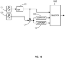
- Fig. 1B illustrates a sideband selector configuration switch 133B according to a related embodiment of the present invention.
- Sideband selector configuration switch 133B selectively switches between the direct output of quadrature modulation block 101 and either the upper sideband of the output of quadrature modulation block 101 mixed via mixer 131 with the output of synthesizer 123, or the lower sideband thereof, as passed by an upper sideband filter 135 or a lower sideband filter 137, respectively.
- transmission signal generation is a hybrid configurable one/two conversion process as illustrated in Fig. 1A .
- the different states reached under the topology depend on the setting of switch 133A and are as follows:
- This architecture inherently features an extremely wide frequency coverage (DC to 10s GHz) while maintaining low spurious signal content.
- the synthesizer frequency range is increased by digital dividers. In these cases, for noise minimization and stability, it may be of interest to have the synthesizers operate at different frequencies. Digitally divided signals, however, typically have high spurious harmonic content. Operation over a multi-octave frequency range normally requires complicated re-configurable filters and filter banks to suppress these spurious signals. By heterodyne down-conversion of the direct modulated signal, wide frequency coverage can be achieved with the spurious signals lying out-of-band.
- a quadrature modulator covering the range 4 - 8 GHz may be mixed with an additional 8 - 12 GHz synthesizer in order to cover the DC - 4 GHz range, and with a 12 - 16 GHz synthesizer in order to cover the 8 - 12 GHz frequency range.
- Higher frequencies may be covered by using up-conversion rather than down-conversion.
- Another benefit provided by embodiments of the present invention is the capability of arbitrarily modulating a wide-band waveform (as wide as the baseband) at any frequency within the frequency coverage.
- This permits the use of modulation schemes such as chirp / pseudo-random bit sequence (PRBS) for pulse compression in radar applications, communication constellations, and so forth.
- PRBS pseudo-random bit sequence
- Another benefit provided by embodiments of the present invention is the ability to reach a certain output frequency via several different configurations.
- Fig. 2 illustrates a signal generator according to another embodiment of the present invention, where a second quadrature modulation block 203 is utilized to directly modulate synthesizer 123 to create the local oscillator for the second conversion. This enables a tradeoff of quadrature modulation imbalance versus phase noise to attain arbitrary frequency in generating the local oscillator for the conversion node.
- Fig. 3 illustrates a multiple signal generator according to an embodiment of the present invention.
- Frequency synthesizer 301 feeds quadrature modulation blocks 303 and 305
- frequency synthesizer 351 feeds quadrature modulation blocks 353 and 355.
- Selector switches 311, 331, 361, and 381 operate as previously described for selector switch 133A ( Fig. 1A ), and selectably switch between the direct output of quadrature modulation blocks 303, 305, 353, and 355 respectively, and outputs of mixers 313, 333, 363, and 383, respectively, all of which receive input from frequency synthesizer 391.
- selector switches 311, 331, 361, and 381 provide selector switches 311, 331, 361, and 381 to be independently switchable.
- Fig. 3 The arrangement illustrated in Fig. 3 is useful in Radar communication systems where there is a need for multiple microwave signals in parallel.
- Non-limiting examples of such needs include:
- Another advantage of this architecture is the distribution of a generated signal among many nodes, such as transmission antennas/receivers etc. This enables applications such as “Multistatic Radar” (see below).
- FIG. 3 Further embodiments of the present invention provide multiple synthesizers (as in Fig. 3 ), some of which are modulated and some are not, so as to simultaneously generate multiple signals at arbitrarily spaced frequencies.
- Fig. 4 illustrates a transceiver according to an embodiment of the present invention.
- a frequency synthesizer 401 feeds quadrature modulator blocks 403 and 405 having selector switches 411 and 431 respectively, which select between direct output from the quadrature modulator blocks and the outputs of mixers 413 and 433, respectively, both of which receive input from a frequency synthesizer 407.
- the output of selector switch 411 feeds into an amplifier 451, which in turn feeds an antenna switch/circulator 453 to an antenna 455 for transmission.
- Signals received from antenna 455 (such as by reflections of the transmitted signal) are fed to a mixer 457, which receives input from switch 431.
- Output of mixer 457 feeds to an anti-aliasing low-pass filter 459 and thence to an analog-to-digital converter 461 (ADC).
- ADC analog-to-digital converter
- both the transmit signal and local oscillator drive for an arbitrary intermediate frequency (IF) receiver are produced.
- the received signal is down-converted to an intermediate frequency corresponding to the offset of the modulation frequency between quadrature modulation blocks 403 and 405.
- arbitrary waveform modulation-based receiver local oscillator generation is a modulation with a pseudo-random binary sequence (PRBS) modulation, for a spread-spectrum radar.
- PRBS pseudo-random binary sequence
- a further example of an arbitrarily-configurable demodulation is multi-tone demodulating. Such a configuration is useful in the simultaneous measurement of several spectral components, e.g. by down-converting them to distinct intermediate frequencies. Both the amplitudes and phases of the spectral components may be measured.
- the above capability of the signal generator for attaining an output frequency in several configurations enables relating measurements across the entire frequency range, i.e. including local oscillator and measured path phase. According to a related embodiment, this is achieved by overlapping measurements between different local oscillator frequencies, where the baseband frequencies are adjusted to account for the local oscillator frequency offset between the measurements.
- This phase-related measurement differs from the common practice in the art, where, as the local oscillator is tuned over the coverage range, unaccounted-for phase changes occur. Retaining the relative phase according to this embodiment is instrumental in characterizing non-linear parameters in a vector network analyzer (VNA) embodiment of the present invention.
- VNA vector network analyzer
- Fig. 5 illustrates a quadrature receiver according to an embodiment of the present invention.
- a switch 511 and a switch 531 are ganged together by a common selector 533, to generate a 0° local oscillator 541 and a 90° local oscillator 543, which feed mixers 561 and 563, respectively, to convert a signal received by an antenna 555, which is amplified by an amplifier 551.
- the two intermediate frequency signals are fed into anti-aliasing low-pass filters 571 and 575, respectively, to be demodulated by analog-to-digital converters 573 and 577, respectively.
- Fig. 5 allows the generation of a 90° split over a wide frequency range, as opposed to conventional analog techniques, and without introducing substantial spurious harmonic content, which occurs when using digital dividers.
- calibration techniques can be used to adjust the relative phase and amplitude between the quadrature channels.
- measuring the phase and amplitude between the in-phase ( I ) and quadrature ( Q ) components of the down-converted continuous wave signal simultaneously measuring the phase and amplitude on several signals; and cross-correlation measurements between the I and Q arms.
- Fig. 6 illustrates a multistatic radar apparatus according to an embodiment of the present invention.
- a generated signal it is desirable for a generated signal to be distributed among many nodes, such as transmission antennas/receivers, and so forth.
- Fig. 7 illustrates a 3-channel multiple input - multiple output (MIMO) transceiver according to an embodiment of the present invention.
- MIMO multiple input - multiple output
- the above-described coherent arbitrary modulation topology is used in conjunction with parallelism (i.e. all quadrature modulation blocks are fed by the same synthesizer and are coherent to each other).
- This configuration enables active beamforming such as in the context of phased-array antennas.
- Current implementations are usable principally in narrow-band arrays, where carrier frequencies reach the microwave regime and analog delay-induced phase shifts are used.
- This embodiment of the present invention provides true beam-forming by digital relative delay means. Beam-forming is achieved by baseband modulation of coherent channels relative to each other, and does not hinder the broad band nature of the transceiver array.
- this embodiment provides ease of implementation with digital accuracy. Steering resolution and phase coherence are very precise since the relative phase attainable at any baseband frequency is practically arbitrary, as it is limited principally by digital-
- Calibration plays a significant role, where quadrature modulation imbalance, local oscillator leakage and the response of the receiver and transmitter paths comprise fundamental factors in attaining the required performance of a transceiver.
- Quadrature modulation imbalance and local oscillator leakage calibrations are typically performed by a minimization of mixing products after passage through a broadband envelope detector.
- the quadrature modulator is subjected to modulation by complex sine wave at frequency f BB .
- the detected power fluctuates at frequencies associated with the frequency offset between the desired signal and the spurious signals (either 2 f BB for the quadrature modulation image or f BB for the local oscillator leakage).
- the power fluctuations are typically measured by an analog-to-digital converter (ADC). It is important to note that if a high f BB is used then a high speed ADC is needed in order to capture and quantify the power fluctuations (the ADC bandwidth needs to be at least twice the baseband bandwidth in order to capture both spectral components).
- Embodiments of the invention facilitate the calibration for quadrature modulation imbalance and local oscillator leakage, without increase in architectural complexity.
- the corrective action for compensation of quadrature modulation imbalance and local oscillator leakage are well known in the art.
- the quadrature modulation imbalance compensation involves pre-multiplying the I and Q components by a matrix of correction coefficients.
- the compensation of local oscillator leakage typically involves adding DC coefficients to the I and Q components. The difficult part of this procedure is determining which coefficients' values to use. This involves a feedback measurement of the strength of the image and spectral components of the local oscillator leakage.
- Fig. 8 illustrates a spectral component measurement arrangement at the output of the signal generation block according to an embodiment of the present invention.
- two quadrature modulation blocks are fed by a single, common, synthesizer.
- a method of measuring the image or local oscillator leakage is by placing the second synthesizer - used to convert the signal to the baseband - at a frequency offset relative to the spectral component of interest.
- Fig. 9 illustrates a receiver-assisted spectral component measurement arrangement according to an embodiment of the present invention.
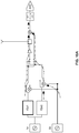
- Fig. 10A illustrates a symmetrized receiver-assisted spectral component measurement arrangement for characterization of a first quadrature modulation block according to the present invention.
- Fig. 10B illustrates a symmetrized receiver-assisted spectral component measurement arrangement for characterization of a second quadrature modulation block according to the present invention.
- Baseband filter characteristics may vary at production. In the case of integrated circuit implementation, the filter bandwidth and shape may depend on process, temperature and voltage. The characteristics of baseband filters in the transmit and receive chains may affect system performance regarding signal-to-noise ratio, inter-symbol interference, power flatness, mask conformity, and so forth. It is thus desirable to characterize the filters and compensate for their deviation from desired characteristics. Examples of compensation include directly adjusting the filter and performing digital compensation.
- the hardware architecture of embodiments of the present invention facilitates measurement of filter characteristics without further increasing complexity.
- the f BB is scanned throughout the range of interest. For each f BB the synthesizer's frequencies ( f sa , f sb ) are adjusted such that the resulting intermediate frequency is constant; thus avoiding the receive filter response variation (when measuring at different intermediate frequencies per f BB ).
- the receiver can be tuned to a frequency corresponding to an aliased frequency ⁇ f BB + N ⁇ f sample (where f sample is the digital-to-analog converter sampling frequency). By doing so, the low pass filter in the transmit path can be characterized beyond the Nyquist frequency of the digital-to-analog converter.
- Embodiments of the invention as described above and depicted in Fig. 8 and Fig. 10A and 10B illustrate two similar schemes for scanning the baseband frequency as described above, by digitizing the output of the signal generation block.
- the quadrature modulation frequency can be tuned to scan the frequencies of the receiver filter.
- the quadrature modulation is held at a constant frequency (so as to not incur response variation) and the receiver frequencies are scanned by tuning the synthesizer's frequencies.
- the intermediate frequency can be tuned beyond the Nyquist frequency of the analog-to-digital converter so that the receive anti-alias low-pass filter reacts to the input intermediate frequency, while the digitized output is at an aliased frequency ⁇ f BB + N ⁇ f sample (where f sample is the analog-to-digital converter sampling frequency.
- f sample is the analog-to-digital converter sampling frequency.
- Digitization of the first synthesizer, down converted by the second synthesizer allows characterizing the relative phase noise between the two synthesizers. This measurement can be used for either self-test purposes or for performance optimizations, such as setting the phase-locked loop parameters so as to optimize the phase noise.
- An example of such parameter is the setting of the charge pump current in the phase detector.
- Fig. 11 illustrates a multi-module referenced based scaling arrangement according to an embodiment of the present invention.
- Fig. 12 is a flowchart 1200 of a method of calibrating a two-synthesizer signal generator according to an embodiment of the present invention.
- the first frequency synthesizer is set to the desired test frequency.
- an outer loop begins, in which the first numerically-controlled oscillator is set to the desired test frequency offset.
- the second frequency synthesizer and the second numerically-controlled oscillator are set to obtain the desired receiving intermediate frequency.
- a step 1207 an inner loop begins for configuring a set of quadrature modulation imbalance correction coefficient values, and in a step 1209 an imbalance-related magnitude is measured.
- a decision point 1211 if the coefficient set is not exhausted, the method returns to step 1207. Otherwise, if the set is exhausted, the loop beginning in step 1207 exits and the method proceeds to a step 1213, in which optimal correction coefficients are calculated.
- step 1215 if the first numerically controlled oscillator frequencies are not exhausted, the method returns to step 1203. Otherwise, if the frequencies are exhausted, the loop beginning in step 1203 exits, and the method concludes with a step 1217, in which the optimal frequency-dependent correction coefficients are calculated.
Landscapes
- Engineering & Computer Science (AREA)
- Computer Networks & Wireless Communication (AREA)
- Signal Processing (AREA)
- Radar, Positioning & Navigation (AREA)
- Remote Sensing (AREA)
- Physics & Mathematics (AREA)
- General Physics & Mathematics (AREA)
- Digital Transmission Methods That Use Modulated Carrier Waves (AREA)
- Noise Elimination (AREA)
- Transceivers (AREA)
- Radar Systems Or Details Thereof (AREA)
Claims (5)
- Signalerzeugende Vorrichtung, umfassend
einen Quadraturmodulationsblock (101), umfassendeinen ersten Digital-Analog-Wandler (103) zum Empfangen von Digitalsignalen, die einer gleichphasigen Wellenformkomponente entsprechen;einen zweiten Digital-Analog-Wandler (107) zum Empfangen von Digitalsignalen, die einer Quadraturwellenformkomponente entsprechen;einen ersten Antialiasing-Tiefpassfilter (105) zum Empfangen eines Ausgangs des ersten Digital-Analog-Wandlers;einen zweiten Antialiasing-Tiefpassfilter (109) zum Empfangen eines Ausgangs des zweiten Digital-Analog-Wandlers;einen ersten Mischer (111; 313) zum Empfangen eines Ausgangs des ersten Antialiasing-Tiefpassfilters;einen zweiten Mischer (313) zum Empfangen eines Ausgangs des zweiten Antialiasing-Tiefpassfilters;einen 90-Grad-Verteilerkasten (115) mit einem Eingang, einem gleichphasigen Ausgang zum Mischen am ersten Mischer und einen Quadraturausgang zum Mischen am zweiten Mischer;einen ersten Frequenzsynthesizer (121; 401) mit einem Ausgang für den Eingang des 90-Grad-Verteilerkastens;eine Summierungseinheit (117) zum Summieren eines Ausgangs des ersten Mischers mit einem Ausgang des zweiten Mischers; undeinen dritten Mischer (131) zum Empfangen eines Ausgangs der Summierungseinheit des Quadraturmodulationsblocks;
einen zweiten Frequenzsynthesizer (123; 407) mit einem Ausgang zum dritten Mischer; und
einen Schalter (133A) mit einem zwischen dem Ausgang der Summierungseinheit und einem Ausgang des dritten Mischers auswählbaren Ausgangs. - Signalerzeugende Vorrichtung nach Anspruch 1, ferner umfassend einen zweiten Quadraturmodulationsblock (203) zum Verbinden des Ausgangs des zweiten Frequenzsynthesizers mit dem dritten Mischer.
- Signalerzeugende Vorrichtung nach Anspruch 1, ferner umfassend eine Vielzahl von Quadraturmodulationsblöcken, wobei jeder dieser Quadraturmodulationsblöcke über einen Ausgang zu einem entsprechenden Mischer und zu einem Schalter mit einem unabhängig zwischen dem Ausgang des entsprechenden Quadraturmodulationsblocks und einem Ausgang des entsprechenden Mischers auswählbaren Ausgang verfügt.
- Signalerzeugende Vorrichtung nach Anspruch 1, ferner umfassend einen oberen Seitenbandfilter (135) oder einen unteren Seitenbandfilter (137) zum Verbinden des Ausgangs des dritten Mischers und des Schalters.
- Sendeempfänger, umfassend
einen ersten Frequenzsynthesizer (401) mit einem Ausgang;
einen ersten Quadraturmodulationsblock (403) zum Empfangen des Ausgangs des ersten Frequenzsynthesizers und mit einem Ausgang zum ersten Mischer (413);
einen ersten Schalter (411) mit einem zwischen dem Ausgang des ersten Quadraturmodulationsblocks und einem Ausgang des ersten Mischers auswählbaren Ausgang;
einen zweiten Quadraturmodulationsblock (405) zum Empfangen des Ausgangs des ersten Frequenzsynthesizers und mit einem Ausgang zu einem zweiten Mischer (433);
einen zweiten Frequenzsynthesizer (407) mit einem Ausgang zum ersten Mischer und zum zweiten Mischer;
einen zweiten Schalter (431) mit einem lokalen Schwingungserzeugerausgang, der zwischen dem Ausgang des zweiten Quadraturmodulationsblocks und einem Ausgang des zweiten Mischers auswählbar ist;
einen Verstärker (451) zum Empfangen eines Eingangs vom ersten Schalter und mit einem Ausgang zu einem Antennenschalter-Zirkulator (453);
einen dritten Mischer (457) zum Empfangen eines Eingangs vom Antennenschalter-Zirkulator und eines Eingangs des lokalen Schwingungserzeugerausgangs vom zweiten Schalter und mit einem Ausgang zu einem Antialiasing-Tiefpassfilter (459); und
einen Digital-Analog-Wandler (461) zum Empfangen des Ausgangs des Antialiasing-Tiefpassfilters;
wobei der erste Schalter und der zweite Schalter unabhängig auswählbar sind.
Priority Applications (2)
| Application Number | Priority Date | Filing Date | Title |
|---|---|---|---|
| EP19174529.8A EP3547534B1 (de) | 2013-09-12 | 2014-09-11 | Vorrichtung und verfahren für signalerzeugung, -empfang und -eigenkalibrierung |
| EP21207177.3A EP4024703A1 (de) | 2013-09-12 | 2014-09-11 | Vorrichtung und verfahren für signalerzeugung, -empfang und -eigenkalibrierung |
Applications Claiming Priority (2)
| Application Number | Priority Date | Filing Date | Title |
|---|---|---|---|
| US201361876949P | 2013-09-12 | 2013-09-12 | |
| PCT/IL2014/050806 WO2015036997A1 (en) | 2013-09-12 | 2014-09-11 | Apparatus and methods for signal generation, reception, and self-calibration |
Related Child Applications (2)
| Application Number | Title | Priority Date | Filing Date |
|---|---|---|---|
| EP21207177.3A Division EP4024703A1 (de) | 2013-09-12 | 2014-09-11 | Vorrichtung und verfahren für signalerzeugung, -empfang und -eigenkalibrierung |
| EP19174529.8A Division EP3547534B1 (de) | 2013-09-12 | 2014-09-11 | Vorrichtung und verfahren für signalerzeugung, -empfang und -eigenkalibrierung |
Publications (3)
| Publication Number | Publication Date |
|---|---|
| EP3044870A1 EP3044870A1 (de) | 2016-07-20 |
| EP3044870A4 EP3044870A4 (de) | 2016-11-09 |
| EP3044870B1 true EP3044870B1 (de) | 2019-05-15 |
Family
ID=52625613
Family Applications (3)
| Application Number | Title | Priority Date | Filing Date |
|---|---|---|---|
| EP14844714.7A Active EP3044870B1 (de) | 2013-09-12 | 2014-09-11 | Vorrichtung und verfahren für signalerzeugung, empfang und eigenkalibrierung |
| EP19174529.8A Not-in-force EP3547534B1 (de) | 2013-09-12 | 2014-09-11 | Vorrichtung und verfahren für signalerzeugung, -empfang und -eigenkalibrierung |
| EP21207177.3A Withdrawn EP4024703A1 (de) | 2013-09-12 | 2014-09-11 | Vorrichtung und verfahren für signalerzeugung, -empfang und -eigenkalibrierung |
Family Applications After (2)
| Application Number | Title | Priority Date | Filing Date |
|---|---|---|---|
| EP19174529.8A Not-in-force EP3547534B1 (de) | 2013-09-12 | 2014-09-11 | Vorrichtung und verfahren für signalerzeugung, -empfang und -eigenkalibrierung |
| EP21207177.3A Withdrawn EP4024703A1 (de) | 2013-09-12 | 2014-09-11 | Vorrichtung und verfahren für signalerzeugung, -empfang und -eigenkalibrierung |
Country Status (6)
| Country | Link |
|---|---|
| US (5) | US9184773B2 (de) |
| EP (3) | EP3044870B1 (de) |
| JP (1) | JP6034996B1 (de) |
| KR (1) | KR101655314B1 (de) |
| CN (2) | CN106105026B (de) |
| WO (1) | WO2015036997A1 (de) |
Families Citing this family (31)
| Publication number | Priority date | Publication date | Assignee | Title |
|---|---|---|---|---|
| US10698095B1 (en) * | 2014-10-17 | 2020-06-30 | California Institute Of Technology | Systems and methods and performing offset IQ modulation |
| US10141974B2 (en) * | 2015-03-17 | 2018-11-27 | Shai Waxman | High-capacity FHSS-MA devices and methods |
| US9525477B1 (en) * | 2015-09-24 | 2016-12-20 | Qualcomm Incorporated | Frequency tracking with sparse pilots |
| US10746851B2 (en) * | 2015-12-18 | 2020-08-18 | Texas Instruments Incorporated | Circuits and methods for determining chirp signal linearity and phase noise of a FMCW radar |
| TWI601397B (zh) * | 2015-12-31 | 2017-10-01 | 瑞昱半導體股份有限公司 | 具牽引效應補償機制的發射器 |
| US10564116B2 (en) | 2016-04-28 | 2020-02-18 | Fluke Corporation | Optical image capture with position registration and RF in-wall composite image |
| US10571591B2 (en) | 2016-04-28 | 2020-02-25 | Fluke Corporation | RF in-wall image registration using optically-sensed markers |
| US10209357B2 (en) | 2016-04-28 | 2019-02-19 | Fluke Corporation | RF in-wall image registration using position indicating markers |
| US10585203B2 (en) | 2016-04-28 | 2020-03-10 | Fluke Corporation | RF in-wall image visualization |
| US10254398B2 (en) | 2016-04-28 | 2019-04-09 | Fluke Corporation | Manipulation of 3-D RF imagery and on-wall marking of detected structure |
| CN106026993B (zh) * | 2016-05-11 | 2019-02-01 | 贵州航天计量测试技术研究所 | 一种宽频带高瞬时带宽信号产生器 |
| US10302793B2 (en) | 2016-08-04 | 2019-05-28 | Fluke Corporation | Blending and display of RF in wall imagery with data from other sensors |
| US10444344B2 (en) | 2016-12-19 | 2019-10-15 | Fluke Corporation | Optical sensor-based position sensing of a radio frequency imaging device |
| US10989806B2 (en) | 2017-03-08 | 2021-04-27 | Praesidium, Inc. | Home occupant detection and monitoring system |
| US11918330B2 (en) | 2017-03-08 | 2024-03-05 | Praesidium, Inc. | Home occupant detection and monitoring system |
| CN109286464B (zh) * | 2017-07-21 | 2022-02-18 | 南京理工大学 | 连续波调频探测抗有源干扰中频信号处理性能测试系统 |
| CN110915151B (zh) * | 2017-08-08 | 2022-10-04 | 日本电信电话株式会社 | 光发送机、光接收机和通信系统 |
| KR102142503B1 (ko) * | 2018-02-12 | 2020-08-07 | 한국항공대학교산학협력단 | Fmcw 레이더의 와이드밴드 신호 송신 장치 및 방법 |
| EP3557769A1 (de) * | 2018-04-18 | 2019-10-23 | Sivers Ima AB | Funkfrequenzsendeempfänger |
| US10663572B2 (en) | 2018-06-19 | 2020-05-26 | Qualcomm Incorporated | Programmable multi-mode digital-to-analog converter (DAC) for wideband applications |
| TWI685669B (zh) | 2018-10-29 | 2020-02-21 | 立積電子股份有限公司 | 雷達裝置及其洩漏修正方法 |
| CN110031810B (zh) * | 2019-04-16 | 2021-02-26 | 北京遥感设备研究所 | 一种单脉冲雷达补偿系数自动校正系统 |
| TWI713313B (zh) | 2019-05-09 | 2020-12-11 | 瑞昱半導體股份有限公司 | 訊號傳輸裝置與校正方法 |
| CN112073113A (zh) * | 2020-08-19 | 2020-12-11 | 北京无线电测量研究所 | 一种星载宽带波形产生组件和方法 |
| TWI739663B (zh) * | 2020-11-16 | 2021-09-11 | 瑞昱半導體股份有限公司 | 校正傳送器的方法 |
| WO2022108375A1 (ko) * | 2020-11-20 | 2022-05-27 | 엘지전자 주식회사 | 무선통신 시스템에서 장치의 신호 전송 방법 및 장치 |
| JP7543894B2 (ja) * | 2020-12-21 | 2024-09-03 | 富士通株式会社 | 無線通信装置及び無線通信方法 |
| EP4395185A4 (de) | 2021-10-15 | 2024-12-25 | Samsung Electronics Co., Ltd. | Elektronische vorrichtung zur ausgabe eines drahtlosen signals auf basis eines chirp-signals durch änderung der frequenz einer frequenzsynthetisierungsschaltung und verfahren dafür |
| TWI864415B (zh) * | 2022-07-08 | 2024-12-01 | 瑞昱半導體股份有限公司 | 具有自我校準機制的收發器裝置及其自我校準方法 |
| DE102023202898A1 (de) * | 2023-03-30 | 2024-10-02 | Robert Bosch Gesellschaft mit beschränkter Haftung | Radartransceiver-Anordnung |
| CN119766165B (zh) * | 2024-12-23 | 2026-03-03 | 四川众为创通科技有限公司 | 基于自适应多制式预校正固态放大器构架及通信设备 |
Family Cites Families (28)
| Publication number | Priority date | Publication date | Assignee | Title |
|---|---|---|---|---|
| DE3569182D1 (en) * | 1985-08-27 | 1989-05-03 | Itt Ind Gmbh Deutsche | Television sound receiving circuit for at least one audio channel contained in a hf signal |
| US5351016A (en) * | 1993-05-28 | 1994-09-27 | Ericsson Ge Mobile Communications Inc. | Adaptively self-correcting modulation system and method |
| JPH0832464A (ja) * | 1994-07-15 | 1996-02-02 | Uniden Corp | 送信機におけるキャリアリーク補正方法 |
| EP0717491B1 (de) * | 1994-12-13 | 2003-02-26 | Hughes Electronics Corporation | Synthetisierer hoher Präzision sowie niedrigen Phasenrauschens, mit Vektormodulator |
| JP3326133B2 (ja) * | 1999-04-02 | 2002-09-17 | 松下電器産業株式会社 | 無線装置及び方法 |
| US6744829B1 (en) * | 2000-09-21 | 2004-06-01 | Koninklijke Philips Electronics N.V. | Calibration of a quadrature receiver |
| KR100457175B1 (ko) * | 2002-12-14 | 2004-11-16 | 한국전자통신연구원 | 직교 변조 송신기 |
| EP1590885A1 (de) * | 2003-01-06 | 2005-11-02 | Sirific Wireless Corporation | Mehrfachmodus-modulator und sender |
| EP1726099A1 (de) * | 2004-03-02 | 2006-11-29 | Koninklijke Philips Electronics N.V. | Serialisierung von mehrband-sequenz-schlüsseln für eine ultrabreitband-empfängerarchitektur mit verringerter komplexität und stromaufnahme |
| WO2007029429A1 (ja) * | 2005-09-06 | 2007-03-15 | Mitsubishi Electric Corporation | 漏洩信号相殺装置 |
| US7542740B1 (en) * | 2005-11-04 | 2009-06-02 | Rf Micro Devices, Inc. | Power amplifier output switch using hybrid combiner |
| JP4686412B2 (ja) * | 2006-07-06 | 2011-05-25 | パナソニック株式会社 | 無線通信装置 |
| US7856048B1 (en) * | 2006-11-20 | 2010-12-21 | Marvell International, Ltd. | On-chip IQ imbalance and LO leakage calibration for transceivers |
| US7844015B2 (en) | 2006-12-18 | 2010-11-30 | Bigband Networks, Inc. | Method for calibrating a quadrature modulator and a modulation system |
| US20090052556A1 (en) | 2007-08-23 | 2009-02-26 | Fernandez Andrew D | Frequency interleaving method for wideband signal generation |
| US8345798B2 (en) * | 2008-05-21 | 2013-01-01 | Entropic Communications, Inc. | Channel stacking system and method of operation |
| US8200181B1 (en) * | 2008-08-29 | 2012-06-12 | Rf Micro Devices, Inc. | Noise reduction in a dual radio frequency receiver |
| KR101017592B1 (ko) * | 2008-11-13 | 2011-02-28 | 엘아이지넥스원 주식회사 | 주파수 합성 장치 및 방법 |
| US8437721B2 (en) * | 2009-04-26 | 2013-05-07 | Qualcomm Incorporated | Jammer detection based adaptive PLL bandwidth adjustment in FM receiver |
| US8599965B2 (en) * | 2009-08-06 | 2013-12-03 | Panasonic Corporation | Wireless communication apparatus |
| WO2011024342A1 (ja) * | 2009-08-26 | 2011-03-03 | パナソニック株式会社 | 送信装置 |
| US20110053537A1 (en) * | 2009-08-31 | 2011-03-03 | Krishnasawamy Nagaraj | Frequency modulation receiver with a low power frequency synthesizer |
| CN101726712B (zh) * | 2009-11-20 | 2012-11-21 | 中国科学院武汉物理与数学研究所 | 射频信号产生装置 |
| CN101771441B (zh) * | 2010-01-19 | 2013-01-02 | 华为技术有限公司 | 室外单元及其提高输出性能的方法 |
| CN102256339B (zh) * | 2010-05-17 | 2014-03-19 | 中兴通讯股份有限公司 | 业务数据传输方法、接收机、移动终端、发射机以及基站 |
| JP6002132B2 (ja) * | 2011-07-19 | 2016-10-05 | 株式会社メガチップス | Iqミスマッチ補正方法およびrf送受信装置 |
| JP2013138308A (ja) * | 2011-12-28 | 2013-07-11 | Anritsu Corp | 信号発生装置及び信号発生方法 |
| US8638893B2 (en) * | 2012-02-24 | 2014-01-28 | National Instruments Corporation | Mechanisms for the correction of I/Q impairments |
-
2014
- 2014-09-11 EP EP14844714.7A patent/EP3044870B1/de active Active
- 2014-09-11 EP EP19174529.8A patent/EP3547534B1/de not_active Not-in-force
- 2014-09-11 JP JP2016531037A patent/JP6034996B1/ja active Active
- 2014-09-11 WO PCT/IL2014/050806 patent/WO2015036997A1/en not_active Ceased
- 2014-09-11 KR KR1020167009655A patent/KR101655314B1/ko active Active
- 2014-09-11 CN CN201480055863.7A patent/CN106105026B/zh active Active
- 2014-09-11 EP EP21207177.3A patent/EP4024703A1/de not_active Withdrawn
- 2014-09-11 CN CN201810350535.XA patent/CN108599786B/zh not_active Expired - Fee Related
- 2014-09-11 US US14/483,295 patent/US9184773B2/en active Active
-
2015
- 2015-09-21 US US14/859,397 patent/US9553621B2/en active Active
-
2017
- 2017-01-24 US US15/413,447 patent/US9813281B2/en active Active
- 2017-11-06 US US15/803,909 patent/US10116486B2/en active Active
-
2018
- 2018-10-28 US US16/172,810 patent/US10461985B2/en not_active Expired - Fee Related
Non-Patent Citations (1)
| Title |
|---|
| None * |
Also Published As
| Publication number | Publication date |
|---|---|
| US9813281B2 (en) | 2017-11-07 |
| US20180062906A1 (en) | 2018-03-01 |
| US9184773B2 (en) | 2015-11-10 |
| US10461985B2 (en) | 2019-10-29 |
| CN108599786A (zh) | 2018-09-28 |
| CN108599786B (zh) | 2021-08-13 |
| KR101655314B1 (ko) | 2016-09-07 |
| CN106105026A (zh) | 2016-11-09 |
| EP3547534B1 (de) | 2021-11-10 |
| KR20160048217A (ko) | 2016-05-03 |
| US20150071381A1 (en) | 2015-03-12 |
| EP3044870A1 (de) | 2016-07-20 |
| US20160020795A1 (en) | 2016-01-21 |
| WO2015036997A1 (en) | 2015-03-19 |
| CN106105026B (zh) | 2018-04-27 |
| EP3044870A4 (de) | 2016-11-09 |
| JP6034996B1 (ja) | 2016-11-30 |
| US10116486B2 (en) | 2018-10-30 |
| JP2016539572A (ja) | 2016-12-15 |
| EP4024703A1 (de) | 2022-07-06 |
| US20170237599A1 (en) | 2017-08-17 |
| US9553621B2 (en) | 2017-01-24 |
| US20190068430A1 (en) | 2019-02-28 |
| EP3547534A1 (de) | 2019-10-02 |
Similar Documents
| Publication | Publication Date | Title |
|---|---|---|
| US10461985B2 (en) | Apparatus and methods for signal generation, reception, and self-calibration | |
| US10794993B2 (en) | Method and apparatus for calibrating an IQ modulator | |
| CN103477570B (zh) | 相控阵发送装置 | |
| EP1671417B1 (de) | Empfänger mit einer oszillationsschaltung zur erzeugung eines bildzurückweisungs-kalibrationstons | |
| US10693687B1 (en) | Intermediate frequency on chip (IFoC) system | |
| US7302237B2 (en) | Wideband signal generators, measurement devices, methods of signal generation, and methods of signal analysis | |
| US20170257137A1 (en) | Active phased array transmitter, active phased array receiver, and active phased array transceiver | |
| JP2011110422A (ja) | 磁気共鳴データの無線通信のためのシステムおよび方法 | |
| US7860196B2 (en) | Method and circuit for estimating in-phase/quadrature signal amplitude imbalance | |
| US8526533B2 (en) | Systems and methods for measuring I-Q mismatch | |
| US20120294343A1 (en) | RF I/Q Modulator with Sampling Calibration System | |
| WO2022175864A1 (en) | Automatic image rejection calibration for radar systems using quadrature transceivers | |
| US12494819B2 (en) | Ultra-wideband signal generator with low phase noise | |
| JP2005304004A (ja) | Pll変調回路及びポーラ変調装置 | |
| JP4376751B2 (ja) | トラッキング発生器及び試験信号発生方法 | |
| US12052061B2 (en) | Mitigation of local oscillator leakage | |
| JP6416818B2 (ja) | Rf信号生成装置およびrf信号解析装置 |
Legal Events
| Date | Code | Title | Description |
|---|---|---|---|
| PUAI | Public reference made under article 153(3) epc to a published international application that has entered the european phase |
Free format text: ORIGINAL CODE: 0009012 |
|
| 17P | Request for examination filed |
Effective date: 20160405 |
|
| AK | Designated contracting states |
Kind code of ref document: A1 Designated state(s): AL AT BE BG CH CY CZ DE DK EE ES FI FR GB GR HR HU IE IS IT LI LT LU LV MC MK MT NL NO PL PT RO RS SE SI SK SM TR |
|
| AX | Request for extension of the european patent |
Extension state: BA ME |
|
| A4 | Supplementary search report drawn up and despatched |
Effective date: 20161010 |
|
| RIC1 | Information provided on ipc code assigned before grant |
Ipc: H03C 1/62 20060101AFI20161004BHEP |
|
| DAX | Request for extension of the european patent (deleted) | ||
| GRAP | Despatch of communication of intention to grant a patent |
Free format text: ORIGINAL CODE: EPIDOSNIGR1 |
|
| STAA | Information on the status of an ep patent application or granted ep patent |
Free format text: STATUS: GRANT OF PATENT IS INTENDED |
|
| INTG | Intention to grant announced |
Effective date: 20181204 |
|
| GRAS | Grant fee paid |
Free format text: ORIGINAL CODE: EPIDOSNIGR3 |
|
| GRAA | (expected) grant |
Free format text: ORIGINAL CODE: 0009210 |
|
| STAA | Information on the status of an ep patent application or granted ep patent |
Free format text: STATUS: THE PATENT HAS BEEN GRANTED |
|
| AK | Designated contracting states |
Kind code of ref document: B1 Designated state(s): AL AT BE BG CH CY CZ DE DK EE ES FI FR GB GR HR HU IE IS IT LI LT LU LV MC MK MT NL NO PL PT RO RS SE SI SK SM TR |
|
| RAP1 | Party data changed (applicant data changed or rights of an application transferred) |
Owner name: VAYYAR IMAGING LTD. |
|
| REG | Reference to a national code |
Ref country code: CH Ref legal event code: EP |
|
| REG | Reference to a national code |
Ref country code: DE Ref legal event code: R096 Ref document number: 602014046980 Country of ref document: DE |
|
| REG | Reference to a national code |
Ref country code: IE Ref legal event code: FG4D |
|
| REG | Reference to a national code |
Ref country code: NL Ref legal event code: MP Effective date: 20190515 |
|
| REG | Reference to a national code |
Ref country code: LT Ref legal event code: MG4D |
|
| PGFP | Annual fee paid to national office [announced via postgrant information from national office to epo] |
Ref country code: LU Payment date: 20190827 Year of fee payment: 6 |
|
| PG25 | Lapsed in a contracting state [announced via postgrant information from national office to epo] |
Ref country code: ES Free format text: LAPSE BECAUSE OF FAILURE TO SUBMIT A TRANSLATION OF THE DESCRIPTION OR TO PAY THE FEE WITHIN THE PRESCRIBED TIME-LIMIT Effective date: 20190515 Ref country code: PT Free format text: LAPSE BECAUSE OF FAILURE TO SUBMIT A TRANSLATION OF THE DESCRIPTION OR TO PAY THE FEE WITHIN THE PRESCRIBED TIME-LIMIT Effective date: 20190915 Ref country code: AL Free format text: LAPSE BECAUSE OF FAILURE TO SUBMIT A TRANSLATION OF THE DESCRIPTION OR TO PAY THE FEE WITHIN THE PRESCRIBED TIME-LIMIT Effective date: 20190515 Ref country code: SE Free format text: LAPSE BECAUSE OF FAILURE TO SUBMIT A TRANSLATION OF THE DESCRIPTION OR TO PAY THE FEE WITHIN THE PRESCRIBED TIME-LIMIT Effective date: 20190515 Ref country code: HR Free format text: LAPSE BECAUSE OF FAILURE TO SUBMIT A TRANSLATION OF THE DESCRIPTION OR TO PAY THE FEE WITHIN THE PRESCRIBED TIME-LIMIT Effective date: 20190515 Ref country code: NL Free format text: LAPSE BECAUSE OF FAILURE TO SUBMIT A TRANSLATION OF THE DESCRIPTION OR TO PAY THE FEE WITHIN THE PRESCRIBED TIME-LIMIT Effective date: 20190515 Ref country code: LT Free format text: LAPSE BECAUSE OF FAILURE TO SUBMIT A TRANSLATION OF THE DESCRIPTION OR TO PAY THE FEE WITHIN THE PRESCRIBED TIME-LIMIT Effective date: 20190515 Ref country code: FI Free format text: LAPSE BECAUSE OF FAILURE TO SUBMIT A TRANSLATION OF THE DESCRIPTION OR TO PAY THE FEE WITHIN THE PRESCRIBED TIME-LIMIT Effective date: 20190515 Ref country code: NO Free format text: LAPSE BECAUSE OF FAILURE TO SUBMIT A TRANSLATION OF THE DESCRIPTION OR TO PAY THE FEE WITHIN THE PRESCRIBED TIME-LIMIT Effective date: 20190815 |
|
| PGFP | Annual fee paid to national office [announced via postgrant information from national office to epo] |
Ref country code: MC Payment date: 20190828 Year of fee payment: 6 |
|
| PG25 | Lapsed in a contracting state [announced via postgrant information from national office to epo] |
Ref country code: RS Free format text: LAPSE BECAUSE OF FAILURE TO SUBMIT A TRANSLATION OF THE DESCRIPTION OR TO PAY THE FEE WITHIN THE PRESCRIBED TIME-LIMIT Effective date: 20190515 Ref country code: GR Free format text: LAPSE BECAUSE OF FAILURE TO SUBMIT A TRANSLATION OF THE DESCRIPTION OR TO PAY THE FEE WITHIN THE PRESCRIBED TIME-LIMIT Effective date: 20190816 Ref country code: LV Free format text: LAPSE BECAUSE OF FAILURE TO SUBMIT A TRANSLATION OF THE DESCRIPTION OR TO PAY THE FEE WITHIN THE PRESCRIBED TIME-LIMIT Effective date: 20190515 Ref country code: BG Free format text: LAPSE BECAUSE OF FAILURE TO SUBMIT A TRANSLATION OF THE DESCRIPTION OR TO PAY THE FEE WITHIN THE PRESCRIBED TIME-LIMIT Effective date: 20190815 |
|
| PGFP | Annual fee paid to national office [announced via postgrant information from national office to epo] |
Ref country code: BE Payment date: 20190716 Year of fee payment: 6 |
|
| REG | Reference to a national code |
Ref country code: AT Ref legal event code: MK05 Ref document number: 1134614 Country of ref document: AT Kind code of ref document: T Effective date: 20190515 |
|
| PGFP | Annual fee paid to national office [announced via postgrant information from national office to epo] |
Ref country code: IS Payment date: 20190807 Year of fee payment: 6 Ref country code: AT Payment date: 20190827 Year of fee payment: 6 |
|
| PG25 | Lapsed in a contracting state [announced via postgrant information from national office to epo] |
Ref country code: DK Free format text: LAPSE BECAUSE OF FAILURE TO SUBMIT A TRANSLATION OF THE DESCRIPTION OR TO PAY THE FEE WITHIN THE PRESCRIBED TIME-LIMIT Effective date: 20190515 Ref country code: RO Free format text: LAPSE BECAUSE OF FAILURE TO SUBMIT A TRANSLATION OF THE DESCRIPTION OR TO PAY THE FEE WITHIN THE PRESCRIBED TIME-LIMIT Effective date: 20190515 Ref country code: SK Free format text: LAPSE BECAUSE OF FAILURE TO SUBMIT A TRANSLATION OF THE DESCRIPTION OR TO PAY THE FEE WITHIN THE PRESCRIBED TIME-LIMIT Effective date: 20190515 Ref country code: CZ Free format text: LAPSE BECAUSE OF FAILURE TO SUBMIT A TRANSLATION OF THE DESCRIPTION OR TO PAY THE FEE WITHIN THE PRESCRIBED TIME-LIMIT Effective date: 20190515 Ref country code: EE Free format text: LAPSE BECAUSE OF FAILURE TO SUBMIT A TRANSLATION OF THE DESCRIPTION OR TO PAY THE FEE WITHIN THE PRESCRIBED TIME-LIMIT Effective date: 20190515 Ref country code: AT Free format text: LAPSE BECAUSE OF FAILURE TO SUBMIT A TRANSLATION OF THE DESCRIPTION OR TO PAY THE FEE WITHIN THE PRESCRIBED TIME-LIMIT Effective date: 20190515 |
|
| REG | Reference to a national code |
Ref country code: DE Ref legal event code: R097 Ref document number: 602014046980 Country of ref document: DE |
|
| PG25 | Lapsed in a contracting state [announced via postgrant information from national office to epo] |
Ref country code: IT Free format text: LAPSE BECAUSE OF FAILURE TO SUBMIT A TRANSLATION OF THE DESCRIPTION OR TO PAY THE FEE WITHIN THE PRESCRIBED TIME-LIMIT Effective date: 20190515 Ref country code: SM Free format text: LAPSE BECAUSE OF FAILURE TO SUBMIT A TRANSLATION OF THE DESCRIPTION OR TO PAY THE FEE WITHIN THE PRESCRIBED TIME-LIMIT Effective date: 20190515 |
|
| PLBE | No opposition filed within time limit |
Free format text: ORIGINAL CODE: 0009261 |
|
| STAA | Information on the status of an ep patent application or granted ep patent |
Free format text: STATUS: NO OPPOSITION FILED WITHIN TIME LIMIT |
|
| PG25 | Lapsed in a contracting state [announced via postgrant information from national office to epo] |
Ref country code: TR Free format text: LAPSE BECAUSE OF FAILURE TO SUBMIT A TRANSLATION OF THE DESCRIPTION OR TO PAY THE FEE WITHIN THE PRESCRIBED TIME-LIMIT Effective date: 20190515 |
|
| 26N | No opposition filed |
Effective date: 20200218 |
|
| PG25 | Lapsed in a contracting state [announced via postgrant information from national office to epo] |
Ref country code: PL Free format text: LAPSE BECAUSE OF FAILURE TO SUBMIT A TRANSLATION OF THE DESCRIPTION OR TO PAY THE FEE WITHIN THE PRESCRIBED TIME-LIMIT Effective date: 20190515 |
|
| PG25 | Lapsed in a contracting state [announced via postgrant information from national office to epo] |
Ref country code: SI Free format text: LAPSE BECAUSE OF FAILURE TO SUBMIT A TRANSLATION OF THE DESCRIPTION OR TO PAY THE FEE WITHIN THE PRESCRIBED TIME-LIMIT Effective date: 20190515 |
|
| REG | Reference to a national code |
Ref country code: CH Ref legal event code: PL |
|
| PG25 | Lapsed in a contracting state [announced via postgrant information from national office to epo] |
Ref country code: LI Free format text: LAPSE BECAUSE OF NON-PAYMENT OF DUE FEES Effective date: 20190930 Ref country code: IE Free format text: LAPSE BECAUSE OF NON-PAYMENT OF DUE FEES Effective date: 20190911 Ref country code: CH Free format text: LAPSE BECAUSE OF NON-PAYMENT OF DUE FEES Effective date: 20190930 |
|
| PG25 | Lapsed in a contracting state [announced via postgrant information from national office to epo] |
Ref country code: MC Free format text: LAPSE BECAUSE OF NON-PAYMENT OF DUE FEES Effective date: 20200930 |
|
| PG25 | Lapsed in a contracting state [announced via postgrant information from national office to epo] |
Ref country code: CY Free format text: LAPSE BECAUSE OF FAILURE TO SUBMIT A TRANSLATION OF THE DESCRIPTION OR TO PAY THE FEE WITHIN THE PRESCRIBED TIME-LIMIT Effective date: 20190515 |
|
| REG | Reference to a national code |
Ref country code: BE Ref legal event code: MM Effective date: 20200930 |
|
| PG25 | Lapsed in a contracting state [announced via postgrant information from national office to epo] |
Ref country code: LU Free format text: LAPSE BECAUSE OF NON-PAYMENT OF DUE FEES Effective date: 20200911 |
|
| PG25 | Lapsed in a contracting state [announced via postgrant information from national office to epo] |
Ref country code: MT Free format text: LAPSE BECAUSE OF FAILURE TO SUBMIT A TRANSLATION OF THE DESCRIPTION OR TO PAY THE FEE WITHIN THE PRESCRIBED TIME-LIMIT Effective date: 20190515 Ref country code: HU Free format text: LAPSE BECAUSE OF FAILURE TO SUBMIT A TRANSLATION OF THE DESCRIPTION OR TO PAY THE FEE WITHIN THE PRESCRIBED TIME-LIMIT; INVALID AB INITIO Effective date: 20140911 |
|
| PG25 | Lapsed in a contracting state [announced via postgrant information from national office to epo] |
Ref country code: BE Free format text: LAPSE BECAUSE OF NON-PAYMENT OF DUE FEES Effective date: 20200930 |
|
| PG25 | Lapsed in a contracting state [announced via postgrant information from national office to epo] |
Ref country code: MK Free format text: LAPSE BECAUSE OF FAILURE TO SUBMIT A TRANSLATION OF THE DESCRIPTION OR TO PAY THE FEE WITHIN THE PRESCRIBED TIME-LIMIT Effective date: 20190515 Ref country code: IS Free format text: LAPSE BECAUSE OF FAILURE TO SUBMIT A TRANSLATION OF THE DESCRIPTION OR TO PAY THE FEE WITHIN THE PRESCRIBED TIME-LIMIT Effective date: 20190915 |
|
| PGFP | Annual fee paid to national office [announced via postgrant information from national office to epo] |
Ref country code: DE Payment date: 20250702 Year of fee payment: 12 |
|
| PGFP | Annual fee paid to national office [announced via postgrant information from national office to epo] |
Ref country code: GB Payment date: 20250703 Year of fee payment: 12 |
|
| PGFP | Annual fee paid to national office [announced via postgrant information from national office to epo] |
Ref country code: FR Payment date: 20250703 Year of fee payment: 12 |