EP3045896A1 - Optischer sensor mit lichtleitender funktion - Google Patents
Optischer sensor mit lichtleitender funktion Download PDFInfo
- Publication number
- EP3045896A1 EP3045896A1 EP16151201.7A EP16151201A EP3045896A1 EP 3045896 A1 EP3045896 A1 EP 3045896A1 EP 16151201 A EP16151201 A EP 16151201A EP 3045896 A1 EP3045896 A1 EP 3045896A1
- Authority
- EP
- European Patent Office
- Prior art keywords
- light
- guiding
- electrical
- optical sensor
- sample
- Prior art date
- Legal status (The legal status is an assumption and is not a legal conclusion. Google has not performed a legal analysis and makes no representation as to the accuracy of the status listed.)
- Granted
Links
Images


Classifications
-
- H—ELECTRICITY
- H10—SEMICONDUCTOR DEVICES; ELECTRIC SOLID-STATE DEVICES NOT OTHERWISE PROVIDED FOR
- H10F—INORGANIC SEMICONDUCTOR DEVICES SENSITIVE TO INFRARED RADIATION, LIGHT, ELECTROMAGNETIC RADIATION OF SHORTER WAVELENGTH OR CORPUSCULAR RADIATION
- H10F30/00—Individual radiation-sensitive semiconductor devices in which radiation controls the flow of current through the devices, e.g. photodetectors
- H10F30/10—Individual radiation-sensitive semiconductor devices in which radiation controls the flow of current through the devices, e.g. photodetectors the devices being sensitive to infrared radiation, visible or ultraviolet radiation, and having no potential barriers, e.g. photoresistors
-
- H—ELECTRICITY
- H10—SEMICONDUCTOR DEVICES; ELECTRIC SOLID-STATE DEVICES NOT OTHERWISE PROVIDED FOR
- H10F—INORGANIC SEMICONDUCTOR DEVICES SENSITIVE TO INFRARED RADIATION, LIGHT, ELECTROMAGNETIC RADIATION OF SHORTER WAVELENGTH OR CORPUSCULAR RADIATION
- H10F77/00—Constructional details of devices covered by this subclass
- H10F77/40—Optical elements or arrangements
- H10F77/413—Optical elements or arrangements directly associated or integrated with the devices, e.g. back reflectors
-
- H—ELECTRICITY
- H10—SEMICONDUCTOR DEVICES; ELECTRIC SOLID-STATE DEVICES NOT OTHERWISE PROVIDED FOR
- H10F—INORGANIC SEMICONDUCTOR DEVICES SENSITIVE TO INFRARED RADIATION, LIGHT, ELECTROMAGNETIC RADIATION OF SHORTER WAVELENGTH OR CORPUSCULAR RADIATION
- H10F39/00—Integrated devices, or assemblies of multiple devices, comprising at least one element covered by group H10F30/00, e.g. radiation detectors comprising photodiode arrays
- H10F39/80—Constructional details of image sensors
- H10F39/806—Optical elements or arrangements associated with the image sensors
-
- G—PHYSICS
- G01—MEASURING; TESTING
- G01J—MEASUREMENT OF INTENSITY, VELOCITY, SPECTRAL CONTENT, POLARISATION, PHASE OR PULSE CHARACTERISTICS OF INFRARED, VISIBLE OR ULTRAVIOLET LIGHT; COLORIMETRY; RADIATION PYROMETRY
- G01J1/00—Photometry, e.g. photographic exposure meter
- G01J1/02—Details
- G01J1/04—Optical or mechanical part supplementary adjustable parts
-
- G—PHYSICS
- G01—MEASURING; TESTING
- G01N—INVESTIGATING OR ANALYSING MATERIALS BY DETERMINING THEIR CHEMICAL OR PHYSICAL PROPERTIES
- G01N21/00—Investigating or analysing materials by the use of optical means, i.e. using sub-millimetre waves, infrared, visible or ultraviolet light
- G01N21/01—Arrangements or apparatus for facilitating the optical investigation
- G01N21/03—Cuvette constructions
- G01N21/0303—Optical path conditioning in cuvettes, e.g. windows; adapted optical elements or systems; path modifying or adjustment
-
- G—PHYSICS
- G01—MEASURING; TESTING
- G01N—INVESTIGATING OR ANALYSING MATERIALS BY DETERMINING THEIR CHEMICAL OR PHYSICAL PROPERTIES
- G01N21/00—Investigating or analysing materials by the use of optical means, i.e. using sub-millimetre waves, infrared, visible or ultraviolet light
- G01N21/62—Systems in which the material investigated is excited whereby it emits light or causes a change in wavelength of the incident light
- G01N21/63—Systems in which the material investigated is excited whereby it emits light or causes a change in wavelength of the incident light optically excited
- G01N21/64—Fluorescence; Phosphorescence
- G01N21/645—Specially adapted constructive features of fluorimeters
- G01N21/648—Specially adapted constructive features of fluorimeters using evanescent coupling or surface plasmon coupling for the excitation of fluorescence
-
- G—PHYSICS
- G01—MEASURING; TESTING
- G01N—INVESTIGATING OR ANALYSING MATERIALS BY DETERMINING THEIR CHEMICAL OR PHYSICAL PROPERTIES
- G01N21/00—Investigating or analysing materials by the use of optical means, i.e. using sub-millimetre waves, infrared, visible or ultraviolet light
- G01N21/75—Systems in which material is subjected to a chemical reaction, the progress or the result of the reaction being investigated
- G01N21/77—Systems in which material is subjected to a chemical reaction, the progress or the result of the reaction being investigated by observing the effect on a chemical indicator
- G01N21/7703—Systems in which material is subjected to a chemical reaction, the progress or the result of the reaction being investigated by observing the effect on a chemical indicator using reagent-clad optical fibres or optical waveguides
-
- G—PHYSICS
- G02—OPTICS
- G02B—OPTICAL ELEMENTS, SYSTEMS OR APPARATUS
- G02B6/00—Light guides; Structural details of arrangements comprising light guides and other optical elements, e.g. couplings
- G02B6/10—Light guides; Structural details of arrangements comprising light guides and other optical elements, e.g. couplings of the optical waveguide type
- G02B6/12—Light guides; Structural details of arrangements comprising light guides and other optical elements, e.g. couplings of the optical waveguide type of the integrated circuit kind
-
- H—ELECTRICITY
- H10—SEMICONDUCTOR DEVICES; ELECTRIC SOLID-STATE DEVICES NOT OTHERWISE PROVIDED FOR
- H10F—INORGANIC SEMICONDUCTOR DEVICES SENSITIVE TO INFRARED RADIATION, LIGHT, ELECTROMAGNETIC RADIATION OF SHORTER WAVELENGTH OR CORPUSCULAR RADIATION
- H10F10/00—Individual photovoltaic cells, e.g. solar cells
-
- H—ELECTRICITY
- H10—SEMICONDUCTOR DEVICES; ELECTRIC SOLID-STATE DEVICES NOT OTHERWISE PROVIDED FOR
- H10F—INORGANIC SEMICONDUCTOR DEVICES SENSITIVE TO INFRARED RADIATION, LIGHT, ELECTROMAGNETIC RADIATION OF SHORTER WAVELENGTH OR CORPUSCULAR RADIATION
- H10F39/00—Integrated devices, or assemblies of multiple devices, comprising at least one element covered by group H10F30/00, e.g. radiation detectors comprising photodiode arrays
- H10F39/80—Constructional details of image sensors
- H10F39/811—Interconnections
-
- H—ELECTRICITY
- H10—SEMICONDUCTOR DEVICES; ELECTRIC SOLID-STATE DEVICES NOT OTHERWISE PROVIDED FOR
- H10F—INORGANIC SEMICONDUCTOR DEVICES SENSITIVE TO INFRARED RADIATION, LIGHT, ELECTROMAGNETIC RADIATION OF SHORTER WAVELENGTH OR CORPUSCULAR RADIATION
- H10F77/00—Constructional details of devices covered by this subclass
- H10F77/93—Interconnections
- H10F77/933—Interconnections for devices having potential barriers
-
- G—PHYSICS
- G01—MEASURING; TESTING
- G01N—INVESTIGATING OR ANALYSING MATERIALS BY DETERMINING THEIR CHEMICAL OR PHYSICAL PROPERTIES
- G01N21/00—Investigating or analysing materials by the use of optical means, i.e. using sub-millimetre waves, infrared, visible or ultraviolet light
- G01N21/75—Systems in which material is subjected to a chemical reaction, the progress or the result of the reaction being investigated
- G01N21/77—Systems in which material is subjected to a chemical reaction, the progress or the result of the reaction being investigated by observing the effect on a chemical indicator
- G01N2021/7753—Reagent layer on photoelectrical transducer
-
- G—PHYSICS
- G01—MEASURING; TESTING
- G01N—INVESTIGATING OR ANALYSING MATERIALS BY DETERMINING THEIR CHEMICAL OR PHYSICAL PROPERTIES
- G01N21/00—Investigating or analysing materials by the use of optical means, i.e. using sub-millimetre waves, infrared, visible or ultraviolet light
- G01N21/75—Systems in which material is subjected to a chemical reaction, the progress or the result of the reaction being investigated
- G01N21/77—Systems in which material is subjected to a chemical reaction, the progress or the result of the reaction being investigated by observing the effect on a chemical indicator
- G01N2021/7769—Measurement method of reaction-produced change in sensor
- G01N2021/7786—Fluorescence
-
- G—PHYSICS
- G01—MEASURING; TESTING
- G01N—INVESTIGATING OR ANALYSING MATERIALS BY DETERMINING THEIR CHEMICAL OR PHYSICAL PROPERTIES
- G01N21/00—Investigating or analysing materials by the use of optical means, i.e. using sub-millimetre waves, infrared, visible or ultraviolet light
- G01N21/62—Systems in which the material investigated is excited whereby it emits light or causes a change in wavelength of the incident light
- G01N21/63—Systems in which the material investigated is excited whereby it emits light or causes a change in wavelength of the incident light optically excited
- G01N21/64—Fluorescence; Phosphorescence
- G01N21/645—Specially adapted constructive features of fluorimeters
- G01N21/6452—Individual samples arranged in a regular 2D-array, e.g. multiwell plates
- G01N21/6454—Individual samples arranged in a regular 2D-array, e.g. multiwell plates using an integrated detector array
-
- G—PHYSICS
- G01—MEASURING; TESTING
- G01N—INVESTIGATING OR ANALYSING MATERIALS BY DETERMINING THEIR CHEMICAL OR PHYSICAL PROPERTIES
- G01N2201/00—Features of devices classified in G01N21/00
- G01N2201/06—Illumination; Optics
- G01N2201/064—Stray light conditioning
- G01N2201/0642—Light traps; baffles
-
- G—PHYSICS
- G02—OPTICS
- G02B—OPTICAL ELEMENTS, SYSTEMS OR APPARATUS
- G02B6/00—Light guides; Structural details of arrangements comprising light guides and other optical elements, e.g. couplings
- G02B6/24—Coupling light guides
- G02B6/42—Coupling light guides with opto-electronic elements
- G02B6/4201—Packages, e.g. shape, construction, internal or external details
- G02B6/4204—Packages, e.g. shape, construction, internal or external details the coupling comprising intermediate optical elements, e.g. lenses, holograms
- G02B6/4214—Packages, e.g. shape, construction, internal or external details the coupling comprising intermediate optical elements, e.g. lenses, holograms the intermediate optical element having redirecting reflective means, e.g. mirrors, prisms for deflecting the radiation from horizontal to down- or upward direction toward a device
-
- Y—GENERAL TAGGING OF NEW TECHNOLOGICAL DEVELOPMENTS; GENERAL TAGGING OF CROSS-SECTIONAL TECHNOLOGIES SPANNING OVER SEVERAL SECTIONS OF THE IPC; TECHNICAL SUBJECTS COVERED BY FORMER USPC CROSS-REFERENCE ART COLLECTIONS [XRACs] AND DIGESTS
- Y02—TECHNOLOGIES OR APPLICATIONS FOR MITIGATION OR ADAPTATION AGAINST CLIMATE CHANGE
- Y02E—REDUCTION OF GREENHOUSE GAS [GHG] EMISSIONS, RELATED TO ENERGY GENERATION, TRANSMISSION OR DISTRIBUTION
- Y02E10/00—Energy generation through renewable energy sources
- Y02E10/50—Photovoltaic [PV] energy
Definitions
- the present disclosure relates to an optical sensor with a light-guiding feature and a method for preparing the same.
- Optical sensors are widely used in various imaging applications and products, such as cameras, scanners, photocopiers and the like. Optical sensors used in various fields of technology are designed for different purposes.
- Quantum efficiency is a percentage of photons hitting the optical sensor that produce charge carriers. It is a measurement of the optical sensor's electrical sensitivity to light.
- One aspect of the present disclosure provides an optical sensor with a light-guiding feature and a method for preparing the same. It is a further object of the present invention to provide a fabrication process for producing such an enhanced light-guiding structure.
- An optical sensor comprises a semiconductive layer comprising an electrical circuit area and an optical sensing area, a sample-holding portion over the optical sensing area, a light-guiding structure between the sample-holding portion and the optical sensing area, and an electrical interconnect structure over the electrical circuit area, wherein the electrical interconnect structure is integrally formed with the light-guiding structure, and the light-guiding structure is configured to direct an emitting light from the sample-holding portion to the optical sensing area.
- the electrical interconnect structure comprises at least one electrical contact over the electrical circuit area
- the light-guiding structure comprises at least one first light-guiding part over the optical sensing area
- the semiconductive layer has a horizontal upper surface, and the at least one electrical contact and the at least one first light-guiding part extend substantially in a same horizontal plane, which is in parallel to and above the horizontal upper surface.
- the light-guiding structure comprises a plurality of first light-guiding parts arranged in a ring.
- the at least one first light-guiding part is a ring-shaped part.
- the electrical interconnect structure comprises at least one electrical via over the at least one electrical contact
- the light-guiding structure comprises at least one second light-guiding part over the at least one first light-guiding part.
- the semiconductive layer has a horizontal upper surface, and the at least one electrical via and the at least one second light-guiding part extend substantially in a same horizontal plane, which is in parallel to and above the horizontal upper surface.
- the light-guiding structure comprises a plurality of second light-guiding parts arranged in a ring.
- the at least one second light-guiding part is a ring-shaped part.
- the light-guiding structure extends from a horizontal upper surface of the semiconductive layer.
- the light-guiding structure comprises an inner light-guiding bar in a first layer over the semiconductive layer and an outer light-guiding bar in a second layer over the semiconductive layer.
- a width of the light-guiding structure is larger in an upper region close to the sample-holding portion than that in a bottom region close to the light-sensing region.
- a width of the light-guiding structure is larger in a bottom region close to the light-sensing region than that in the upper region close to the sample-holding portion.
- An optical sensor comprises a semiconductive layer comprising an electrical circuit area and an optical sensing area, a sample-holding portion over the optical sensing area, at least one electrical contact over the electrical circuit area, and at least one first light-guiding part configured to direct an emitting light from the sample-holding portion to the optical sensing area, wherein the semiconductive layer has a horizontal upper surface, the at least one first light-guiding part is between the sample-holding portion and the optical sensing area, and the at least one electrical contact and the at least one first light-guiding part extend substantially in a same horizontal plane, which is in parallel to and above the horizontal upper surface.
- the at least one electrical contact is integrally formed with the at least one first light-guiding part.
- An optical sensor comprises a semiconductive layer comprising an optical sensing area, a sample-holding portion over the optical sensing area, and a light-guiding structure configured to direct an emitting light from the sample-holding portion to the optical sensing area, wherein the light-guiding structure comprises at least one light-guiding spacer extending from a horizontal upper surface of the semiconductive layer, and the light-guiding structure has a tapering top end near the sample-holding portion.
- the light-guiding structure comprises a plurality of light-guiding spacers arranged in a ring.
- the light-guiding structure comprises a ring-shaped guiding spacer.
- the optical sensor comprises a plurality of dielectric layers over the optical sensing area, wherein the at least one light-guiding spacer extends through the plurality of dielectric layers.
- the light-guiding structure has a sidewall tilted with respect to the semiconductive layer, and an included angle between the horizontal upper surface of the semiconductive layer and the sidewall is about 60 degrees to 89.5 degrees.
- the light-guiding structure is designed to prevent light scattering. Due to the design of the light-guiding structure, the emitting light from the sample-holding portion can be more efficiently directed to the light-sensing region in the optical sensing area. Furthermore, the fabrication of the light-guiding structure complies with the back-end-of-line (BEOL) metallization technology and can be fabricated by the same fabrication process in the same die as the electrical interconnected structure and the multi-junction photodiode of the light-sensing region. In addition, the light-guiding structure, the electrical interconnect structure and the multi-junction photodiode of the light-sensing region are integrated in the same die by the same fabrication process rather than in two separated devices. Thus, the size of the optical sensor can be dramatically decreased.
- BEOL back-end-of-line
- references to "one embodiment,” “an embodiment,” “exemplary embodiment,” “other embodiments,” “another embodiment,” etc. indicate that the embodiment(s) of the disclosure so described may include a particular feature, structure, or characteristic, but not every embodiment necessarily includes the particular feature, structure, or characteristic. Further, repeated use of the phrase “in the embodiment” does not necessarily refer to the same embodiment, although it may.
- the present disclosure is directed to an optical sensor with a light-guiding feature.
- detailed steps and structures are provided in the following description. Obviously, implementation of the present disclosure does not limit special details known by persons skilled in the art. In addition, known structures and steps are not described in detail, so as not to limit the present disclosure unnecessarily. Preferred embodiments of the present disclosure will be described below in detail. However, in addition to the detailed description, the present disclosure may also be widely implemented in other embodiments. The scope of the present disclosure is not limited to the detailed description, and is defined by the claims.
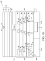
- FIG. 1A is a cross-sectional view of an optical sensor 100 in accordance with some embodiments of the present disclosure.
- the optical sensor 100 comprises a semiconductive layer 111 having an electrical circuit area 111A and an optical sensing area 111B, a sample-holding portion 23 over the optical sensing area 111B, a light-guiding structure 130 between the sample-holding portion 23 and the optical sensing area 111B, and an electrical interconnect structure 140 over the electrical circuit area 111A.
- the light-guiding structure 130 is configured to direct an emitting light from the sample-holding portion 23 to the optical sensing area 111B.
- the semiconductive layer 111 is a silicon substrate including a light-sensing region 55 in the optical sensing area 111Bused for detecting light of various wavelengths, and the sample holding portion 23 is used for holding a specimen 231 under analysis.
- the sample holding portion 23 is disposed in a waveguide structure 120 over the light-guiding structure 130, and the light-sensing region 55 is a multi-junction photodiode disposed in an epitaxy region below the light-guiding structure 130.
- the light-sensing region 55 in the semiconductive layer 111 and the sample holding portion 23 in a waveguide structure 120 are disclosed in U.S.
- the specimen 231 When a light 8 having wavelengths from around 450 nanometers to around 500 nanometers shines on the specimen 231 in the sample holding portion 23, the specimen 231 emits lights81 such as fluorescent lights, and the light-guiding structure 130 is configured to direct the emitting lights81 to the light-sensing region 55.
- the wavelength of the emitted fluorescent light for example, can be a characteristic of a material in the specimen 231.
- the specimen 231 emits fluorescent lights with different wavelengths.
- the light-sensing region 55 is electrically connected to the electrical interconnect structure 140through conductor so as to transfer the charge carriers generated in the light sensing region 55 to the electrical circuitry in the electrical interconnect structure 140 for further signal processing and/or output to signal-processing electronics, such as a DSP or microprocessor.
- signal-processing electronics such as a DSP or microprocessor.
- the electrical interconnect structure 140 is integrally formed with the light-guiding structure 130. In some embodiments, the correspondingly elements of the electrical interconnect structure 140 and the light-guiding structure 130 are formed substantially by the same fabrication process, and have substantially the same physical and chemical properties.
- the electrical interconnect structure 140 comprises at least one electrical contact 141 over the electrical circuit area 111A
- the light-guiding structure 130 comprises at least one first light-guiding part 131 over the optical sensing area 111B.
- the first light-guiding part 131 is simultaneously formed with the electrical contact 141 substantially by the same fabrication process and the same material, and the first light-guiding part 131 and the electrical interconnect contact 141 have substantially the same physical and chemical properties.
- the semiconductive layer 111 has a horizontal upper surface 112, and the electrical contact 141 and the first light-guiding part131 extend substantially in a same horizontal plane, which is in parallel to and above the horizontal upper surface 112.
- the optical sensor 100 has a dielectric layer 101 over the horizontal upper surface 112, and the electrical contact 141 and the first light-guiding part 131 are positioned in the dielectric layer 101.
- the bottom ends of the electrical contact 141 and the first light-guiding part 131 are substantially at the same level, the upper ends of the electrical contact 141 and the first light-guiding part 131 are substantially at the same level; thus, the electrical contact 141 and the first light-guiding part 131 can be formed through the same fabrication process.
- the electrical interconnect structure 140 comprises at least one electrical via 142 over the electrical contact 141
- the light-guiding structure 130 comprises at least one second light-guiding part 132 over the first light-guiding part 131.
- the second light-guiding part 132 is simultaneously formed with the electrical via 142 substantially by the same fabrication process and the same material, and the second light-guiding part 132and the electrical via 142 have substantially the same physical and chemical properties.
- the electrical interconnect structure 140 has an electrical metal layer 143 between the electrical via 142 and the electrical contact 141; similarly, the light-guiding structure 130 has a third light-guiding part 133 between the second light-guiding part 132 and the first light-guiding part 131.
- the third light-guiding part 133 is simultaneously formed with the electrical metal layer 143 substantially by the same fabrication process and the same material, and the third light-guiding part 133 and the electrical metal layer 143 have substantially the same physical and chemical properties.
- the electrical via 142 and the second light-guiding part 132 extend substantially in a same horizontal plane, which is in parallel to and above the horizontal upper surface 112.
- the optical sensor 100 has a dielectric layer 102 over the horizontal upper surface 112, and the electrical via 142 and the second light-guiding part 132 are positioned in the dielectric layer 102.
- the bottom ends of the electrical metal layer 143 and the third light-guiding part 133 are substantially at the same level, the upper ends of the electrical via 142 and the second light-guiding part 132 are substantially at the same level; thus, the electrical contact 141 and the first light-guiding part 131 can be formed through the same fabrication processes.
- the optical sensor 100 has a plurality of dielectric layers 102-104 over the dielectric layer 101, and each dielectric layer has at least one electrical via 142 and at least one second light-guiding part 132 extending substantially in a same horizontal plane.
- the second light-guiding part 132 can be optionally implemented in some of the dielectric layers, rather than in all of the dielectric layers.
- the light-guiding structure 130 extends vertically or in a tilt manner from the horizontal upper surface 112 of the semiconductive layer 111.
- the horizontal distance between the second light-guiding parts 132 in the upper dielectric layer 104 is larger than that in the lower dielectric layer 102; in other words, the horizontal distance shrinks along a light-propagating direction from the sample-holding portion 23 to the light-sensing region 55.
- FIG. IB is a cross-sectional view of an optical sensor 100' in accordance with some embodiments of the present disclosure.
- the optical sensor 100' shown in FIG. 1B is substantially the same as the optical sensor 100 shown in FIG. 1A , except the design of the light-guiding structure.
- the width of the light-guiding structure 130 is larger in the upper region (close to the sample-holding portion 23) than that in the bottom region (close to the light-sensing region 55); in contrast, in FIG. 1B , the width of the light-guiding structure 130' is larger in the bottom region (close to the light-sensing region 55) than that in the upper region (close to the sample-holding portion 23).
- FIG. 1C is a cross-sectional view of an optical sensor 100" in accordance with some embodiments of the present disclosure.
- the optical sensor 100" shown in FIG. 1C is substantially the same as the optical sensor 100 shown in FIG. 1A , except the design of the light-guiding structure.
- the width of the light-guiding structure 130 is larger in the upper region (close to the sample-holding portion 23) than that in the bottom region (close to the light-sensing region 55); in contrast, in FIG. 1C , the width of the light-guiding structure 130" in the bottom region (close to the light-sensing region 55) is substantially the same as that in the upper region (close to the sample-holding portion 23).
- the inner sidewall of the light-guiding structure 130" is substantially vertical to the horizontal upper surface 112.
- FIG. 2 is a top view of a light-guiding structure 130A in accordance with some embodiments of the present disclosure.
- the light-guiding structure 130A comprises a ring-shaped first light-guiding part 131A and a ring-shaped second light-guiding part 132A.
- the ring-shaped first light-guiding part 131A can be optionally disposed inside or outside of the ring-shaped second light-guiding part 132A, and more second light-guiding parts can be optionally disposed in the light-guiding structure 130A.
- the outer periphery of the ring-shaped first light-guiding part 131A can be optionally overlapped with the inner periphery of the ring-shaped second light-guiding part132A where the ring-shaped first light-guiding part 131A is disposed inside the ring-shaped second light-guiding part 132A, or vice versa.
- FIG. 3 is a top view of a light-guiding structure 130B in accordance with some embodiments of the present disclosure.
- the light-guiding structure 130B comprises a plurality of first light-guiding parts 131B arranged in a ring, and a plurality of second light-guiding parts 132B arranged in a ring.
- the plurality of first light-guiding part 131B can be optionally disposed inside or outside of the plurality of second light-guiding parts 132B, and more second light-guiding parts can be optionally disposed in the light-guiding structure 130B.
- the outer periphery of the first light-guiding part 131B can be optionally overlapped with the inner periphery of the second light-guiding part 132B where the first light-guiding part 131B is disposed inside the second light-guiding part 132B, or vice versa.
- FIG. 4 is a top view of a light-guiding structure 130C in accordance with some embodiments of the present disclosure.
- the light-guiding structure 130C comprises an inner light-guiding bar 131C serving as the first light-guiding partin the dielectric layer 101 over the semiconductive layer 111 and an outer light-guiding bar 132C serving as the second light-guiding partin the dielectric layer 102 over the semiconductive layer 111.
- the light-guiding bar 131C can be optionally disposed inside or outside of the light-guiding bar 132C, and more light-guiding bars can be optionally disposed in the light-guiding structure 130C.
- the outer periphery of the inner light-guiding bar can be optionally overlapped with the inner periphery of the outer light-guiding bar.
- each of the light-guiding bars 131C can be further laterally divided into serval parts; similarly, each of the light-guiding bars 132C can be further laterally divided into serval parts.
- the light-guiding bars 131C can be optionally connected to form an integral rectangular light-guiding ring, and the light-guiding bars 132C can be optionally connected to form an integral rectangular light-guiding ring.
- the emitting light 81 from the sample-holding portion 23 can be more efficiently directed to the light-sensing region 55 in the optical sensing area 111B.
- the fabrication of the light-guiding structure 130, the electrical interconnect structure 140,and the multi-junction photodiode of the light-sensing region 55 comply with the back-end-of-line (BEOL) metallization technology, and can be fabricated by the same fabrication process in the same die.
- the light-guiding structure 130, the electrical interconnect structure 140,and the multi-junction photodiode of the light-sensing region are integrated in the same die by the same fabrication process rather than in two separated devices.
- the size of the optical sensor 100 can be dramatically decreased.
- FIG. 5 to FIG. 10 are cross-sectional views for preparing an optical sensor in accordance with some embodiments of the present disclosure.
- the fabrication processes disclosed in FIG. 5 to FIG. 10 comply with the aluminum back-end-of-line (BEOL) metallization technology.
- BEOL aluminum back-end-of-line
- a light-sensing region 55 is formed in a semiconductivelayer111, electronic devices 149 such as transistors are formed over an electrical circuit area 111A, and an inter-layer dielectric layer 101 is then formed on the semiconductive layer 111 by deposition and planarization processes. Subsequently, lithographic, etching, deposition and planarization processes are performed to form electrical contacts 141 over the electrical circuit area 111A and form first light-guiding parts 131 over the optical sensing area 111B.
- the electrical contact 141 and the first light-guiding part 131 include tungsten (W).
- deposition, lithographic and etching processes are performed to form anelectrical metal layer 143 over the electrical contact 141 and form a third light-guiding part 133 over the first light-guiding part 131.
- the electrical metal layer 143 and the third light-guiding part 133 include aluminum (Al).
- an inter-metal dielectric layer 102 is formed on the inter-layer dielectric layer 101 by deposition and planarization processes.
- the inter-metal dielectric layer 102 includes a lower portion 102A formed by an HDP deposition process and an upper layer 102B formed by a PECVD process.
- lithographic, etching, deposition and planarization processes are performed to form electrical vias 142 over the electrical contacts 141 and form second light-guiding parts 132 over the first light-guiding parts 131.
- the electrical via 142 and the second light-guiding part 132 include tungsten (W).
- a metal layer 147 having an opening 147A is formed by fabrication processes including deposition, lithographic and etching processes, wherein the opening 147A can be a rectangular opening.
- the metal layer 147 serves as a light shielding layer, wherein the opening 147A exposes the light sensing region 55 for receiving the light from the sample-holding portion 23, while the metal layer 147 covers the other regions.
- the metal layer 147 can serve as a contact pad for forming electrical connection to an external printed circuit board (PCB) by wire bonding.
- the thickness of the metal layer 147 is larger than that of the metal layer below, and the thickness of the metal layer 147 is preferably larger than 4,000 angstroms.
- dielectric deposition and planarization processes are performed to form a dielectric layer 106 on the metal layer 147 and fills the opening 147A.
- the dielectric deposition is a PECVD process
- the planarization is an oxide CMP process.
- the dielectric deposition includes a spin-on glass (SOG), SOG curing, SOG etching back, and a PECVD process.
- the dielectric layer106 includes silicon oxide or silicon nitride, and silicon nitride is preferred for absorbing background light having a wavelength of 488 nanometers.
- a deposition process is performed to form a filter layer 119 over the inter-metal dielectric layer105.
- deposition processes are performed to form a lower cladding layer 121 and a core layer 123 over the filter layer 119; subsequently, deposition, lithographic and etching processes are performed to an upper cladding layer 125 having a sample-holding portion 23 over the light sensing region 55.
- the refractive index of the core layer 123 is higher than that of the cladding layers 121 and 125.
- the filter layer 119 is transparent to the wavelength emitted from the specimen 231, and the emitting light 81 from the sample-holding portion 23 travels through the filter layer 119 toward the light-sensing region 55.
- the lower cladding layer 121, the core layer 123, and the upper cladding layer 125 form a waveguide structure 120.
- the lower cladding layer 121 and the upper cladding layer 125 include oxide such as SiO 2 .
- the core layer 123 includes dielectric such as Ta 2 O 5 or SiON.
- the embodiment shown in FIG. 5 to FIG. 10 is characterized in integrally forming the light-guiding structure(first light-guiding part, second light-guiding part, third light-guiding part) and the electrical interconnect structure(electrical contact, electrical via, electrical metal layer), i.e., substantially by the same fabrication process and the same material simultaneously, and the corresponding elements of the light-guiding structure and the electrical interconnect structure have substantially the same physical and chemical properties.
- integrally forming the light-guiding structure and the electrical interconnect structure not only decreases the fabrication cost, but also simplify the fabrication process.
- FIG. 11A is a cross-sectional view of an optical sensor 200 in accordance with some embodiments of the present disclosure.
- the optical sensor 200 comprises a semiconductive layer 111 comprising an electrical circuit area 111A and an optical sensing area 111B, a sample-holding portion 23 over the optical sensing area 111B, an electrical interconnect structure 240 including at least one electrical contact 141 over the electrical circuit area 111A, and a light-guiding structure 230 including at least one first light-guiding part 131 between the sample-holding portion 23 and the optical sensing area 111A.
- the electrical interconnect structure 240 is integrally formed with the light-guiding structure 230.
- the elements of the electrical interconnect structure 240 and the elements of the light-guiding structure 230 are formed substantially by the same fabrication process, and have substantially the same physical and chemical properties.
- the first light-guiding part 131 is simultaneously formed with the electrical contact 141 substantially by the same fabrication process and the same material, and the first light-guiding part 131 and the electrical interconnect contact 141 have substantially the same physical and chemical properties.
- the semiconductive layer 111 has a horizontal upper surface 112, the at least one electrical contact 141 and the at least one first light-guiding part 131 extend substantially in a same horizontal plane, which is in parallel to and above the horizontal upper surface 112, and the light-guiding structure 230 is configured to direct an emitting light 81 from the sample-holding portion 23 to the optical sensing area 111A.
- the optical sensor 200 comprises an inter-layer dielectric layer 101 and a plurality of inter-metal dielectric layers202-205, wherein the inter-layer dielectric layer 101 has the electrical contact 141 and the first light-guiding part 131, while the inter-metal dielectric layers 202-205 have at least one electrical via 242 and at least one electrical metal layer 243 over the electrical circuit area 111A, and at least one second light-guiding part232 and at least one third light-guiding part 233 over the optical sensing area 111B.
- the light-guiding structure 230 can use the ring-shaped layout shown in FIG. 3 , the part layout in a ring shown in FIG. 4 , or the bar layout shown in FIG. 5 .
- the third light-guiding part233 is simultaneously formed with the electrical metal layer243 substantially by the same fabrication process and the same material, and the third light-guiding part233 and the electrical metal layer243 have substantially the same physical and chemical properties.
- the electrical metal layer 243 and the third light-guiding part 233 extend substantially in a same horizontal plane, which is in parallel to and above the horizontal upper surface 112. The upper ends of the electrical metal layer 243 and the third light-guiding part 233 are substantially at the same level, and the bottom ends of the electrical metal layer 243 and the third light-guiding part 233 are substantially at the same level, and they can be formed through the same fabrication processes.
- the second light-guiding part232 is simultaneously formed with the electrical via 242 substantially by the same fabrication process and the same material, and the second light-guiding part232and the electrical via 242 have substantially the same physical and chemical properties.
- the electrical via 242 and the second light-guiding part 232 extend substantially in a same horizontal plane, which is in parallel to and above the horizontal upper surface 112. The upper ends of the electrical via 242 and the second light-guiding part 232 are substantially at the same level, and the bottom ends of the electrical via 242 and the second light-guiding part 232 are substantially at the same level, and they can be formed through the same fabrication processes.
- the second light-guiding part 232 can be optionally implemented in some of the dielectric layers, rather than in all of the dielectric layers.
- the horizontal distance between the second light-guiding parts 232 in the upper dielectric layer 205 is larger than that in the lower dielectric layer 203; in other words, the horizontal distance shrinks along a light-propagating direction from the sample-holding portion 23 to the light-sensing region 55 in the optical sensing area 111B.
- the light-guiding structure 230 extends vertically or in a tilt manner from the horizontal upper surface 112 of the semiconductive layer 111.
- the light-sensing region 55 is electrically connected to the electrical interconnect structure 240 through conductor so as to transfer the charge carriers generated in the light sensing region 55 to the electrical circuitry in the electrical interconnect structure 240 for further signal processing and/or output to signal-processing electronics, such as a DSP or microprocessor.
- signal-processing electronics such as a DSP or microprocessor.
- FIG. 11B is a cross-sectional view of an optical sensor 200' in accordance with some embodiments of the present disclosure.
- the optical sensor 200' shown in FIG. 11B is substantially the same as the optical sensor 200 shown in FIG. 11A , except the design of the light-guiding structure.
- the width of the light-guiding structure 230 is larger in the upper region (close to the sample-holding portion 23) than that in the bottom region (close to the light-sensing region 55); in contrast, in FIG. 11B , the width of the light-guiding structure 230' is larger in the bottom region (close to the light-sensing region 55) than that in the upper region (close to the sample-holding portion 23).
- FIG. 11C is a cross-sectional view of an optical sensor 200" in accordance with some embodiments of the present disclosure.
- the optical sensor 200" shown in FIG. 11C is substantially the same as the optical sensor 200 shown in FIG. 11A , except the design of the light-guiding structure.
- the width of the light-guiding structure 230 is larger in the upper region (close to the sample-holding portion 23) than that in the bottom region (close to the light-sensing region 55); in contrast, in FIG. 11C , the width of the light-guiding structure 230" in the bottom region (close to the light-sensing region 55) is substantially the same as that in the upper region (close to the sample-holding portion 23).
- the inner sidewall of the light-guiding structure 230" is substantially vertical to the horizontal upper surface 112.
- the emitting light 81 from the sample-holding portion 23 can be more efficiently directed to the light-sensing region 55 in the optical sensing area 111B.
- the fabrication of the light-guiding structure 230, the electrical interconnect structure 240and the multi-junction photodiode of the light-sensing region 55 comply with the back-end-of-line (BEOL) metallization technology, and can be fabricated by the same fabrication process in the same die.
- the light-guiding structure 230, the electrical interconnect structure 240,and the multi-junction photodiode of the light-sensing region 55 are integrated in the same die by the same fabrication process rather than in two separated devices.
- the size of the optical sensor 200 can be dramatically decreased.
- FIG. 12 to FIG. 17 are cross-sectional views for preparing an optical sensor in accordance with some embodiments of the present disclosure.
- the fabrication processes disclosed in FIG. 12 to FIG. 17 comply with the copper back-end-of-line (BEOL) metallization technology.
- BEOL copper back-end-of-line
- a light-sensing region 55 is formed in a semiconductivelayer111, electronic devices 149 such as transistors are formed over an electrical circuit area 111A, and an inter-layer dielectric layer 101 is then formed on the semiconductive layer 111 by deposition and planarization processes. Subsequently, lithographic, etching, deposition and planarization processes are performed to form electrical contacts 141 over the electrical circuit area 111A and form first light-guiding parts 131 over the optical sensing area 111B.
- deposition, lithographic and etching processes are performed to form an inter-metal dielectric layer 202 having an aperture 2021A and an aperture 2021B, which expose the first light-guiding part 131 over the electrical circuit area 111A and the electrical contact 141 over the optical sensing area 111B.
- deposition and planarization processes are performed to form at least one electrical metal layer243 in the aperture 2021A over the electrical contact 141 and form at least one third light-guiding part233 in the aperture 2021B over the first light-guiding part 131.
- the electrical metal layer 243 and the third light-guiding part 233 include copper (Cu).
- deposition, lithographic and etching processes are performed to form an inter-metal dielectric layer 203 over the inter-metal dielectric layer 202.
- deposition and planarization processes are performed to form an electricalvia242 over the electrical contact 141 and form a second light-guiding part 232 over the first light-guiding part 131.
- the electrical metal layer 243 and the third light-guiding part 233 include copper (Cu).
- a metal layer 147 having an opening 147A is formed by fabrication processes including deposition, lithographic and etching processes, wherein the opening 147A can be a rectangular opening.
- the metal layer 147 serves as a light shielding layer, wherein the opening 147A exposes the light sensing region 55 for receiving the light from the sample-holding portion 23, while the metal layer 147 covers the other regions.
- the metal layer 147 can serve as a contact pad for forming electrical connection to an external printed circuit board (PCB) by wire bonding.
- the thickness of the metal layer 147 is larger than that of the metal layer below, and the thickness of the metal layer 147 is preferably larger than 4,000 angstroms.
- dielectric deposition and planarization processes are performed to form a dielectric layer106 on the metal layer 147 and fills the opening 147A.
- the dielectric deposition is a PECVD process
- the planarization is an oxide CMP process.
- the dielectric deposition includes a spin-on glass (SOG), SOG curing, SOG etching back, and a PECVD process.
- the dielectric layer106 includes silicon oxide or silicon nitride, and silicon nitride is preferred for absorbing background light having a wavelength of 488 nanometers.
- a deposition process is performed to form a filter layer 119 over the inter-metal dielectric layer 205.
- deposition processes are performed to form a lower cladding layer 121 and a core layer 123 over the filter layer 119; subsequently, deposition, lithographic and etching processes are performed to an upper cladding layer 125 having a sample-holding portion 23 over the light sensing region 55.
- the filter layer 119 is transparent to the wavelength emitted from the specimen 231, and the emitting light 81 from the sample-holding portion 23 travels through the filter layer 119 toward the light-sensing region 55.
- the lower cladding layer 121, the core layer 123, and the upper cladding layer 125 form a waveguide structure 120.
- the lower cladding layer 121 and the upper cladding layer 125 include oxide such as SiO 2 .
- the core layer 123 includes dielectric such as Ta 2 O 5 or SiON.
- the embodiment shown in FIG. 12 to FIG. 17 is characterized in integrally forming the light-guiding structure(first light-guiding part, second light-guiding part, third light-guiding part) and the electrical interconnect structure(electrical contact, electrical via, electrical metal layer), i.e., substantially by the same fabrication process and the same material simultaneously, and the corresponding elements of the light-guiding structure and the electrical interconnect structure have substantially the same physical and chemical properties.
- integrally forming the light-guiding structure and the electrical interconnect structure not only decreases the fabrication cost, but also simplify the fabrication process.
- FIG. 18A is a cross-sectional view of an optical sensor 300 in accordance with some embodiments of the present disclosure.
- the optical sensor 300 comprises a semiconductive layer 111 having an optical sensing area 111B, a sample-holding portion 23 over the optical sensing area 111B, and a light-guiding structure 330 configured to direct an emitting light 81 from the sample-holding portion 23 to the optical sensing area 111B.
- the light-guiding structure 330 comprises at least one light-guiding spacer 331 and extends from a horizontal upper surface 112 of the semiconductive layer 111, and the light-guiding structure 330 has a tapering top end 332 near the sample-holding portion 23.
- the optical sensor 100 has a plurality of dielectric layers 101-105 over the optical sensing area 111B, and the light-guiding spacer 331 is a wall extending from the horizontal upper surface 112 of the semiconductive layer 111 through the plurality of dielectric layers 101-105.
- the light-guiding spacer 331 can optionally extend vertically or in a tilt manner from the horizontal upper surface 112 through the plurality of dielectric layers 101-105.
- the light-guiding structure 330 can use the ring-shaped layout shown in FIG. 3 , the part layout in a ring shown in FIG. 4 , or the bar layout shown in FIG. 5 .
- FIG. 18B is a cross-sectional view of an optical sensor 300' in accordance with some embodiments of the present disclosure.
- the optical sensor 300' shown in FIG. 18B is substantially the same as the optical sensor 300 shown in FIG. 18A , except the design of the light-guiding structure.
- the sidewall 331 of the light-guiding structure 330' is tilted with respect to the semiconductive layer 111, wherein the included angle ( ⁇ ) between the horizontal upper surface 112 of the semiconductive layer 111 and the sidewall 331 of the light-guiding structure 330' is about 60degrees to 89.5degrees.
- the emitting light 81 from the sample-holding portion 23 can be more efficiently directed to the light-sensing region 55 in the optical sensing area 111B.
- the fabrication of the light-guiding structure 330 complies with the back-end-of-line (BEOL) metallization technology, and can be fabricated by the same fabrication process in the same die as the electrical interconnected structure 140 and the multi-junction photodiode of the light-sensing region 55.
- the light-guiding structure 130, the electrical interconnect structure 140 and the multi-junction photodiode of the light-sensing region 55 are integrated in the same die by the same fabrication process rather than in two separated devices.
- the size of the optical sensor 300 can be dramatically decreased.
- FIG. 19 to FIG. 23 are cross-sectional views for preparing an optical sensor in accordance with some embodiments of the present disclosure.
- the fabrication processes disclosed in FIG. 19 to FIG. 23 comply with both the aluminum back-end-of-line (BEOL) metallization technology and the copper back-end-of-line (BEOL) metallization technology.
- BEOL aluminum back-end-of-line
- BEOL copper back-end-of-line
- a light-sensing region 55 is formed in a semiconductivelayer111, and electronic devices 149 such as transistors are formed over an electrical circuit area 111A. Subsequently, lithographic, etching, deposition and planarization processes are performed to form an electrical interconnect structure 140 having electrical contacts 141, electrical metal layers 143, and electrical vias 142 over an electrical circuit area 111A of the semiconductivelayer 11.
- lithographic and etching processes are performed to form an aperture 301 over the light-sensing region 55 in the optical sensing area 111B.
- a metal disposition process is performed to form a metal layer 302 on the sidewall of the aperture 301 and the upper surface of the dielectric layer 105.
- a metal etching back process is performed to remove a portion of the metal layer 302 to form a metal spacer on the sidewall of the aperture 301.
- dielectric deposition and planarization processes are performed to form a dielectric layer 303 filling the aperture 301.
- the dielectric layer 303 includes dielectric such as silicon oxide or silicon nitride, and silicon nitride is preferred for absorbing background light having a wavelength of 488 nanometers.
- a metal layer 147 having an opening 147A is formed by fabrication processes including deposition, lithographic and etching processes, wherein the opening 147A can be a rectangular opening.
- the metal layer 147 serves as a light shielding layer, wherein the opening 147A exposes the light sensing region 55 for receiving the light from the sample-holding portion 23, while the metal layer 147 covers the other regions.
- the metal layer 147 can serve as a contact pad for forming electrical connection to an external printed circuit board (PCB) by wire bonding.
- the thickness of the metal layer 147 is larger than that of the metal layer below, and the thickness of the metal layer 147 is preferably larger than 4,000 angstroms.
- dielectric deposition and planarization processes are performed to form a dielectric layer304 on the metal layer 147 and fills the aperture 301 and the opening 147A.
- the dielectric deposition is a PECVD process
- the planarization is an oxide CMP process.
- the dielectric deposition includes a spin-on glass (SOG), SOG curing, SOG etching back, and a PECVD process.
- the dielectric layer304 includes dielectric such as silicon oxide or silicon nitride, and silicon nitride is preferred for absorbing background light having a wavelength of 488 nanometers.
- a deposition process is performed to form a filter layer 119 over the inter-metal dielectric layer 105.
- deposition processes are performed to form a lower cladding layer 121 and a core layer 123 over the filter layer 119; subsequently, deposition, lithographic and etching processes are performed to an upper cladding layer 125 having a sample-holding portion 23 over the light sensing region 55.
- the filter layer 119 is transparent to the wavelength emitted from the specimen 231, and the emitting light 81 from the sample-holding portion 23 travels through the filter layer 119 toward the light-sensing region 55.
- the lower cladding layer 121, the core layer 123, and the upper cladding layer 125 form a waveguide structure 120.
- the lower cladding layer 121 and the upper cladding layer 125 include oxide such as SiO 2 .
- the core layer 123 includes dielectric such as Ta 2 O 5 or SiON.
- the optical sensor includes a semiconductive layer comprising an electrical circuit area and an optical sensing area, a sample-holding portion over the optical sensing area, a light-guiding structure between the sample-holding portion and the optical sensing area, and an electrical interconnect structure over the electrical circuit area.
- the electrical interconnect structure is integrally formed with the light-guiding structure, and the light-guiding structure is configured to direct an emitting light from the sample-holding portion to the optical sensing area.
- the optical sensor includes a semiconductive layer comprising an electrical circuit area and an optical sensing area, a sample-holding portion over the optical sensing area, at least one electrical contact over the electrical circuit area, and at least one first light-guiding part configured to direct an emitting light from the sample-holding portion to the optical sensing area.
- the semiconductive layer has a horizontal upper surface, the at least one first light-guiding part is between the sample-holding portion and the optical sensing area, and the at least one electrical contact and the at least one first light-guiding part extend substantially in a same horizontal plane, which is in parallel to and above the horizontal upper surface.
- the optical sensor includes a semiconductive layer comprising an optical sensing area, a sample-holding portion over the optical sensing area, and a light-guiding structure configured to direct an emitting light from the sample-holding portion to the optical sensing area.
- the light-guiding structure comprises at least one light-guiding spacer and extends from a horizontal upper surface of the semiconductive layer, and the light-guiding structure has a tapering top end near the sample-holding portion.
- the light-guiding structure is designed to prevent light scattering. Due to the design of the light-guiding structure, the emitting light from the sample-holding portion can be more efficiently directed to the light-sensing region in the optical sensing area. Furthermore, the fabrication of the light-guiding structure complies with the back-end-of-line (BEOL) metallization technology, and can be fabricated by the same fabrication process in the same die as the electrical interconnected structure and the multi-junction photodiode of the light-sensing region. In addition, the light-guiding structure, the electrical interconnect structure and the multi-junction photodiode of the light-sensing region are integrated in the same die by the same fabrication process rather than in two separated devices. Thus, the size of the optical sensor can be dramatically decreased.
- BEOL back-end-of-line
- An optical sensor comprising: a semiconductive layer comprising an optical sensing area; a sample-holding portion over the optical sensing area; and a light-guiding structure configured to direct an emitting light from the sample-holding portion to the optical sensing area; wherein the light-guiding structure comprises at least one light-guiding spacer extending from a horizontal upper surface of the semiconductive layer, and the light-guiding structure has a tapering top end near the sample-holding portion.
- the optical sensor of Embodiment A wherein the light-guiding structure comprises a plurality of light-guiding spacers arranged in a ring.
- the optical sensor of Embodiment A or B wherein the light-guiding structure comprises a ring-shaped guiding part.
- optical sensor of any of Embodiments A to C comprising a plurality of dielectric layers over the optical sensing area, wherein the at least one light-guiding spacer extends through the plurality of dielectric layers.
- optical sensor of any of Embodiments A to D wherein the light-guiding structure has a sidewall tilted with respect to the semiconductive layer, and an included angle between the horizontal upper surface of the semiconductive layer and the sidewall is about 60 degrees to 89.5 degrees.
Landscapes
- Physics & Mathematics (AREA)
- General Physics & Mathematics (AREA)
- Health & Medical Sciences (AREA)
- Chemical & Material Sciences (AREA)
- Life Sciences & Earth Sciences (AREA)
- Analytical Chemistry (AREA)
- Biochemistry (AREA)
- General Health & Medical Sciences (AREA)
- Immunology (AREA)
- Pathology (AREA)
- Engineering & Computer Science (AREA)
- Nuclear Medicine, Radiotherapy & Molecular Imaging (AREA)
- Plasma & Fusion (AREA)
- Chemical Kinetics & Catalysis (AREA)
- Spectroscopy & Molecular Physics (AREA)
- Optics & Photonics (AREA)
- Microelectronics & Electronic Packaging (AREA)
- Solid State Image Pick-Up Elements (AREA)
- Investigating, Analyzing Materials By Fluorescence Or Luminescence (AREA)
- Investigating Or Analysing Materials By Optical Means (AREA)
- Light Receiving Elements (AREA)
- Optical Integrated Circuits (AREA)
- Optical Measuring Cells (AREA)
Applications Claiming Priority (1)
| Application Number | Priority Date | Filing Date | Title |
|---|---|---|---|
| US201562104340P | 2015-01-16 | 2015-01-16 |
Publications (3)
| Publication Number | Publication Date |
|---|---|
| EP3045896A1 true EP3045896A1 (de) | 2016-07-20 |
| EP3045896C0 EP3045896C0 (de) | 2023-06-07 |
| EP3045896B1 EP3045896B1 (de) | 2023-06-07 |
Family
ID=55177751
Family Applications (1)
| Application Number | Title | Priority Date | Filing Date |
|---|---|---|---|
| EP16151201.7A Active EP3045896B1 (de) | 2015-01-16 | 2016-01-14 | Optischer sensor mit lichtleitender funktion |
Country Status (7)
| Country | Link |
|---|---|
| US (2) | US20160211390A1 (de) |
| EP (1) | EP3045896B1 (de) |
| JP (2) | JP2016133510A (de) |
| KR (2) | KR20160088821A (de) |
| CN (1) | CN105810701B (de) |
| AU (1) | AU2016200223B2 (de) |
| TW (1) | TWI591324B (de) |
Cited By (3)
| Publication number | Priority date | Publication date | Assignee | Title |
|---|---|---|---|---|
| EP3644365A1 (de) * | 2018-10-25 | 2020-04-29 | ams International AG | Vorrichtung mit optischem sensor und verfahren zur herstellung einer vorrichtung mit optischem sensor |
| WO2021026291A1 (en) * | 2019-08-08 | 2021-02-11 | Quantum-Si Incorporated | Increased emission collection efficiency in integrated optical devices |
| US12203853B2 (en) | 2019-06-19 | 2025-01-21 | Quantum-Si Incorporated | Optical nanostructure rejecter for an integrated device and related methods |
Families Citing this family (10)
| Publication number | Priority date | Publication date | Assignee | Title |
|---|---|---|---|---|
| EP4113104A3 (de) | 2016-06-01 | 2023-02-22 | Quantum-si Incorporated | Integrierte vorrichtung zur detektion und analyse von molekülen |
| TWI669811B (zh) * | 2018-02-01 | 2019-08-21 | Powerchip Semiconductor Manufacturing Corporation | 具有類光導管結構之影像感測器 |
| TWI739119B (zh) * | 2018-06-21 | 2021-09-11 | 昇佳電子股份有限公司 | 光學感測模組 |
| EP4038426B1 (de) * | 2019-09-30 | 2026-03-18 | California Institute of Technology | Integrierte elektronisch-photonische bauelemente, systeme und verfahren zu deren herstellung |
| KR102228480B1 (ko) | 2020-05-14 | 2021-03-16 | 주식회사 케이티 서비스 북부 | 안전사다리 |
| GB2595671B (en) * | 2020-06-02 | 2022-10-19 | X Fab Global Services Gmbh | Optical sensor comprising a photodiode array |
| KR102835582B1 (ko) | 2020-07-27 | 2025-07-16 | 삼성전자주식회사 | 이미지 센서 |
| WO2022076894A1 (en) | 2020-10-08 | 2022-04-14 | Avicenatech Corp. | Integration of oe devices with ics |
| US12249662B2 (en) * | 2022-05-20 | 2025-03-11 | Taiwan Semiconductor Manufacturing Company, Ltd. | Semiconductor device, manufacturing method thereof, and detecting method using the same |
| KR102672313B1 (ko) * | 2022-07-08 | 2024-06-05 | 한국전자통신연구원 | 전자파 간섭 제거 기능을 갖는 수광 소자 |
Citations (4)
| Publication number | Priority date | Publication date | Assignee | Title |
|---|---|---|---|---|
| US20040234417A1 (en) * | 2001-09-17 | 2004-11-25 | Infineon Technologies Ag | Fluorescence biosensor chip and fluorescence biosensor chip arrangement |
| US20080081769A1 (en) * | 2006-08-24 | 2008-04-03 | Arjang Hassibi | Integrated Semiconductor Bioarray |
| US20140001341A1 (en) * | 2012-06-28 | 2014-01-02 | Board Of Regents, The University Of Texas System | Integrated optical biosensor array |
| WO2014031157A1 (en) * | 2012-08-20 | 2014-02-27 | Illumina, Inc. | Method and system for fluorescence lifetime based sequencing |
Family Cites Families (25)
| Publication number | Priority date | Publication date | Assignee | Title |
|---|---|---|---|---|
| US6197503B1 (en) * | 1997-11-26 | 2001-03-06 | Ut-Battelle, Llc | Integrated circuit biochip microsystem containing lens |
| TW494574B (en) | 1999-12-01 | 2002-07-11 | Innotech Corp | Solid state imaging device, method of manufacturing the same, and solid state imaging system |
| JP3827909B2 (ja) * | 2000-03-21 | 2006-09-27 | シャープ株式会社 | 固体撮像装置およびその製造方法 |
| US7140058B2 (en) * | 2002-09-27 | 2006-11-28 | Colgate-Palmolive Company | Toothbrush with kinetic plate |
| TWI236767B (en) * | 2002-12-13 | 2005-07-21 | Sony Corp | Solid-state image pickup device and its manufacturing method |
| US6861686B2 (en) * | 2003-01-16 | 2005-03-01 | Samsung Electronics Co., Ltd. | Structure of a CMOS image sensor and method for fabricating the same |
| KR100745985B1 (ko) * | 2004-06-28 | 2007-08-06 | 삼성전자주식회사 | 이미지 센서 |
| EP1622200A1 (de) * | 2004-07-26 | 2006-02-01 | CSEM Centre Suisse d'Electronique et de Microtechnique SA | Festkörper-Fotodetektor-Pixel und Fotodetektionsverfahren |
| US7193289B2 (en) * | 2004-11-30 | 2007-03-20 | International Business Machines Corporation | Damascene copper wiring image sensor |
| JP5005179B2 (ja) * | 2005-03-23 | 2012-08-22 | ソニー株式会社 | 固体撮像装置 |
| US7683407B2 (en) * | 2005-08-01 | 2010-03-23 | Aptina Imaging Corporation | Structure and method for building a light tunnel for use with imaging devices |
| WO2007129451A1 (ja) * | 2006-04-26 | 2007-11-15 | National University Corporation NARA Institute of Science and Technology | イメージセンサ |
| KR100781545B1 (ko) * | 2006-08-11 | 2007-12-03 | 삼성전자주식회사 | 감도가 향상된 이미지 센서 및 그의 제조방법 |
| US7537951B2 (en) * | 2006-11-15 | 2009-05-26 | International Business Machines Corporation | Image sensor including spatially different active and dark pixel interconnect patterns |
| JP2008235689A (ja) * | 2007-03-22 | 2008-10-02 | Sharp Corp | 固体撮像素子およびその製造方法、電子情報機器 |
| WO2009057075A2 (en) * | 2007-11-01 | 2009-05-07 | Insiava (Pty) Ltd | Optoelectronic device with light directing arrangement and method of forming the arrangement |
| JP5357441B2 (ja) | 2008-04-04 | 2013-12-04 | キヤノン株式会社 | 固体撮像装置の製造方法 |
| EP2221606A3 (de) * | 2009-02-11 | 2012-06-06 | Samsung Electronics Co., Ltd. | Integrierter Biochip und Verfahren zur Herstellung des integrierten Biochips |
| JP5050063B2 (ja) * | 2010-01-20 | 2012-10-17 | 株式会社東芝 | 固体撮像装置 |
| EP3460458B1 (de) * | 2010-02-19 | 2021-08-11 | Pacific Biosciences of California, Inc. | Verfahren zur nukleinsäuresequenzierung |
| US9482615B2 (en) * | 2010-03-15 | 2016-11-01 | Industrial Technology Research Institute | Single-molecule detection system and methods |
| US20120156100A1 (en) * | 2010-12-20 | 2012-06-21 | Industrial Technology Research Institute | Apparatus for single molecule detection and method thereof |
| JP5274678B2 (ja) * | 2011-02-09 | 2013-08-28 | キヤノン株式会社 | 光電変換素子、およびこれを用いた光電変換装置、撮像システム |
| JP5810565B2 (ja) * | 2011-03-16 | 2015-11-11 | セイコーエプソン株式会社 | 光学センサー及び電子機器 |
| US9624540B2 (en) * | 2013-02-22 | 2017-04-18 | Pacific Biosciences Of California, Inc. | Integrated illumination of optical analytical devices |
-
2016
- 2016-01-14 EP EP16151201.7A patent/EP3045896B1/de active Active
- 2016-01-14 KR KR1020160004945A patent/KR20160088821A/ko not_active Ceased
- 2016-01-14 AU AU2016200223A patent/AU2016200223B2/en active Active
- 2016-01-14 JP JP2016005091A patent/JP2016133510A/ja active Pending
- 2016-01-14 US US14/996,037 patent/US20160211390A1/en not_active Abandoned
- 2016-01-15 CN CN201610028259.6A patent/CN105810701B/zh active Active
- 2016-01-15 TW TW105101180A patent/TWI591324B/zh active
-
2017
- 2017-11-20 JP JP2017222488A patent/JP6546639B2/ja active Active
-
2018
- 2018-06-21 KR KR1020180071315A patent/KR101994331B1/ko active Active
-
2019
- 2019-10-28 US US16/665,352 patent/US11362223B2/en active Active
Patent Citations (4)
| Publication number | Priority date | Publication date | Assignee | Title |
|---|---|---|---|---|
| US20040234417A1 (en) * | 2001-09-17 | 2004-11-25 | Infineon Technologies Ag | Fluorescence biosensor chip and fluorescence biosensor chip arrangement |
| US20080081769A1 (en) * | 2006-08-24 | 2008-04-03 | Arjang Hassibi | Integrated Semiconductor Bioarray |
| US20140001341A1 (en) * | 2012-06-28 | 2014-01-02 | Board Of Regents, The University Of Texas System | Integrated optical biosensor array |
| WO2014031157A1 (en) * | 2012-08-20 | 2014-02-27 | Illumina, Inc. | Method and system for fluorescence lifetime based sequencing |
Cited By (8)
| Publication number | Priority date | Publication date | Assignee | Title |
|---|---|---|---|---|
| EP3644365A1 (de) * | 2018-10-25 | 2020-04-29 | ams International AG | Vorrichtung mit optischem sensor und verfahren zur herstellung einer vorrichtung mit optischem sensor |
| WO2020083606A1 (en) * | 2018-10-25 | 2020-04-30 | Ams International Ag | Optical sensor device and method for manufacturing an optical sensor device |
| US12087780B2 (en) | 2018-10-25 | 2024-09-10 | Ams International Ag | Optical sensor device and method for manufacturing an optical sensor device |
| US12203853B2 (en) | 2019-06-19 | 2025-01-21 | Quantum-Si Incorporated | Optical nanostructure rejecter for an integrated device and related methods |
| WO2021026291A1 (en) * | 2019-08-08 | 2021-02-11 | Quantum-Si Incorporated | Increased emission collection efficiency in integrated optical devices |
| US11454758B2 (en) | 2019-08-08 | 2022-09-27 | Quantum-Si Incorporated | Optical microdisks for integrated devices |
| US11977257B2 (en) | 2019-08-08 | 2024-05-07 | Quantum-Si Incorporated | Optical microdisks for integrated devices |
| US12366706B2 (en) | 2019-08-08 | 2025-07-22 | Quantum-Si Incorporated | Optical microdisks for integrated devices |
Also Published As
| Publication number | Publication date |
|---|---|
| TW201627651A (zh) | 2016-08-01 |
| CN105810701A (zh) | 2016-07-27 |
| US20200066926A1 (en) | 2020-02-27 |
| JP2016133510A (ja) | 2016-07-25 |
| JP6546639B2 (ja) | 2019-07-17 |
| KR20160088821A (ko) | 2016-07-26 |
| KR101994331B1 (ko) | 2019-09-30 |
| CN105810701B (zh) | 2019-10-18 |
| TWI591324B (zh) | 2017-07-11 |
| AU2016200223A1 (en) | 2016-08-04 |
| EP3045896C0 (de) | 2023-06-07 |
| JP2018054623A (ja) | 2018-04-05 |
| US11362223B2 (en) | 2022-06-14 |
| KR20180075454A (ko) | 2018-07-04 |
| EP3045896B1 (de) | 2023-06-07 |
| US20160211390A1 (en) | 2016-07-21 |
| AU2016200223B2 (en) | 2017-02-09 |
Similar Documents
| Publication | Publication Date | Title |
|---|---|---|
| US11362223B2 (en) | Method for manufacturing an optical sensor | |
| CN109768056B (zh) | 图像传感装置的形成方法 | |
| CN109786409B (zh) | 影像感测装置及其形成方法 | |
| US11990493B2 (en) | Image sensor device with reflective structure | |
| US10276616B2 (en) | Image sensor device | |
| US7646943B1 (en) | Optical waveguides in image sensors | |
| KR102288339B1 (ko) | 반도체 이미지 센서 | |
| US20160178840A1 (en) | Optical waveguides in image sensors | |
| CN119967921A (zh) | 半导体图像传感器 | |
| US11698296B2 (en) | Light sensor using pixel optical diffraction gratings having different pitches | |
| US20120236313A1 (en) | Spectroscopic sensor and angle limiting filter | |
| CN109564925B (zh) | 具有集成光传感器的片上系统型相机以及制造片上系统型相机的方法 | |
| KR100937662B1 (ko) | 이미지 센서 및 그 제조 방법 | |
| CN106057838A (zh) | 半导体结构及其制造方法 | |
| DE112013002559T5 (de) | Spektralsensor | |
| CN102891159B (zh) | Cmos影像传感器的像元结构及其制造方法 | |
| CN100502022C (zh) | 半导体装置 | |
| US9214485B2 (en) | Thick multilayer interference filter having a lower metal layer located within an interconnect region | |
| KR20200101450A (ko) | 광검출기 및 이의 제조 방법, 이미지 센서 | |
| CN112992996B (zh) | 一种显示面板及显示装置 | |
| KR20090072036A (ko) | 이미지 센서 및 그 제조 방법 | |
| CN119521816A (zh) | 影像传感器 |
Legal Events
| Date | Code | Title | Description |
|---|---|---|---|
| PUAI | Public reference made under article 153(3) epc to a published international application that has entered the european phase |
Free format text: ORIGINAL CODE: 0009012 |
|
| AK | Designated contracting states |
Kind code of ref document: A1 Designated state(s): AL AT BE BG CH CY CZ DE DK EE ES FI FR GB GR HR HU IE IS IT LI LT LU LV MC MK MT NL NO PL PT RO RS SE SI SK SM TR |
|
| AX | Request for extension of the european patent |
Extension state: BA ME |
|
| STAA | Information on the status of an ep patent application or granted ep patent |
Free format text: STATUS: REQUEST FOR EXAMINATION WAS MADE |
|
| 17P | Request for examination filed |
Effective date: 20161125 |
|
| RBV | Designated contracting states (corrected) |
Designated state(s): AL AT BE BG CH CY CZ DE DK EE ES FI FR GB GR HR HU IE IS IT LI LT LU LV MC MK MT NL NO PL PT RO RS SE SI SK SM TR |
|
| STAA | Information on the status of an ep patent application or granted ep patent |
Free format text: STATUS: EXAMINATION IS IN PROGRESS |
|
| 17Q | First examination report despatched |
Effective date: 20181011 |
|
| REG | Reference to a national code |
Ref country code: DE Ref legal event code: R079 Ref document number: 602016079788 Country of ref document: DE Free format text: PREVIOUS MAIN CLASS: G01N0021770000 Ipc: G01N0021640000 |
|
| GRAP | Despatch of communication of intention to grant a patent |
Free format text: ORIGINAL CODE: EPIDOSNIGR1 |
|
| STAA | Information on the status of an ep patent application or granted ep patent |
Free format text: STATUS: GRANT OF PATENT IS INTENDED |
|
| RIC1 | Information provided on ipc code assigned before grant |
Ipc: G02B 6/42 20060101ALN20221031BHEP Ipc: G01N 21/77 20060101ALI20221031BHEP Ipc: G01N 21/64 20060101AFI20221031BHEP |
|
| INTG | Intention to grant announced |
Effective date: 20221118 |
|
| GRAS | Grant fee paid |
Free format text: ORIGINAL CODE: EPIDOSNIGR3 |
|
| GRAA | (expected) grant |
Free format text: ORIGINAL CODE: 0009210 |
|
| STAA | Information on the status of an ep patent application or granted ep patent |
Free format text: STATUS: THE PATENT HAS BEEN GRANTED |
|
| AK | Designated contracting states |
Kind code of ref document: B1 Designated state(s): AL AT BE BG CH CY CZ DE DK EE ES FI FR GB GR HR HU IE IS IT LI LT LU LV MC MK MT NL NO PL PT RO RS SE SI SK SM TR |
|
| REG | Reference to a national code |
Ref country code: GB Ref legal event code: FG4D |
|
| REG | Reference to a national code |
Ref country code: CH Ref legal event code: EP Ref country code: AT Ref legal event code: REF Ref document number: 1576541 Country of ref document: AT Kind code of ref document: T Effective date: 20230615 |
|
| REG | Reference to a national code |
Ref country code: DE Ref legal event code: R096 Ref document number: 602016079788 Country of ref document: DE |
|
| U01 | Request for unitary effect filed |
Effective date: 20230607 |
|
| U07 | Unitary effect registered |
Designated state(s): AT BE BG DE DK EE FI FR IT LT LU LV MT NL PT SE SI Effective date: 20230612 |
|
| REG | Reference to a national code |
Ref country code: LT Ref legal event code: MG9D |
|
| PG25 | Lapsed in a contracting state [announced via postgrant information from national office to epo] |
Ref country code: NO Free format text: LAPSE BECAUSE OF FAILURE TO SUBMIT A TRANSLATION OF THE DESCRIPTION OR TO PAY THE FEE WITHIN THE PRESCRIBED TIME-LIMIT Effective date: 20230907 Ref country code: ES Free format text: LAPSE BECAUSE OF FAILURE TO SUBMIT A TRANSLATION OF THE DESCRIPTION OR TO PAY THE FEE WITHIN THE PRESCRIBED TIME-LIMIT Effective date: 20230607 |
|
| PG25 | Lapsed in a contracting state [announced via postgrant information from national office to epo] |
Ref country code: RS Free format text: LAPSE BECAUSE OF FAILURE TO SUBMIT A TRANSLATION OF THE DESCRIPTION OR TO PAY THE FEE WITHIN THE PRESCRIBED TIME-LIMIT Effective date: 20230607 Ref country code: HR Free format text: LAPSE BECAUSE OF FAILURE TO SUBMIT A TRANSLATION OF THE DESCRIPTION OR TO PAY THE FEE WITHIN THE PRESCRIBED TIME-LIMIT Effective date: 20230607 Ref country code: GR Free format text: LAPSE BECAUSE OF FAILURE TO SUBMIT A TRANSLATION OF THE DESCRIPTION OR TO PAY THE FEE WITHIN THE PRESCRIBED TIME-LIMIT Effective date: 20230908 |
|
| PG25 | Lapsed in a contracting state [announced via postgrant information from national office to epo] |
Ref country code: SK Free format text: LAPSE BECAUSE OF FAILURE TO SUBMIT A TRANSLATION OF THE DESCRIPTION OR TO PAY THE FEE WITHIN THE PRESCRIBED TIME-LIMIT Effective date: 20230607 |
|
| PG25 | Lapsed in a contracting state [announced via postgrant information from national office to epo] |
Ref country code: IS Free format text: LAPSE BECAUSE OF FAILURE TO SUBMIT A TRANSLATION OF THE DESCRIPTION OR TO PAY THE FEE WITHIN THE PRESCRIBED TIME-LIMIT Effective date: 20231007 |
|
| U20 | Renewal fee for the european patent with unitary effect paid |
Year of fee payment: 9 Effective date: 20231219 |
|
| PG25 | Lapsed in a contracting state [announced via postgrant information from national office to epo] |
Ref country code: SM Free format text: LAPSE BECAUSE OF FAILURE TO SUBMIT A TRANSLATION OF THE DESCRIPTION OR TO PAY THE FEE WITHIN THE PRESCRIBED TIME-LIMIT Effective date: 20230607 Ref country code: SK Free format text: LAPSE BECAUSE OF FAILURE TO SUBMIT A TRANSLATION OF THE DESCRIPTION OR TO PAY THE FEE WITHIN THE PRESCRIBED TIME-LIMIT Effective date: 20230607 Ref country code: RO Free format text: LAPSE BECAUSE OF FAILURE TO SUBMIT A TRANSLATION OF THE DESCRIPTION OR TO PAY THE FEE WITHIN THE PRESCRIBED TIME-LIMIT Effective date: 20230607 Ref country code: IS Free format text: LAPSE BECAUSE OF FAILURE TO SUBMIT A TRANSLATION OF THE DESCRIPTION OR TO PAY THE FEE WITHIN THE PRESCRIBED TIME-LIMIT Effective date: 20231007 Ref country code: CZ Free format text: LAPSE BECAUSE OF FAILURE TO SUBMIT A TRANSLATION OF THE DESCRIPTION OR TO PAY THE FEE WITHIN THE PRESCRIBED TIME-LIMIT Effective date: 20230607 |
|
| PG25 | Lapsed in a contracting state [announced via postgrant information from national office to epo] |
Ref country code: PL Free format text: LAPSE BECAUSE OF FAILURE TO SUBMIT A TRANSLATION OF THE DESCRIPTION OR TO PAY THE FEE WITHIN THE PRESCRIBED TIME-LIMIT Effective date: 20230607 |
|
| REG | Reference to a national code |
Ref country code: DE Ref legal event code: R097 Ref document number: 602016079788 Country of ref document: DE |
|
| PLBE | No opposition filed within time limit |
Free format text: ORIGINAL CODE: 0009261 |
|
| STAA | Information on the status of an ep patent application or granted ep patent |
Free format text: STATUS: NO OPPOSITION FILED WITHIN TIME LIMIT |
|
| 26N | No opposition filed |
Effective date: 20240308 |
|
| PG25 | Lapsed in a contracting state [announced via postgrant information from national office to epo] |
Ref country code: MC Free format text: LAPSE BECAUSE OF FAILURE TO SUBMIT A TRANSLATION OF THE DESCRIPTION OR TO PAY THE FEE WITHIN THE PRESCRIBED TIME-LIMIT Effective date: 20230607 |
|
| PG25 | Lapsed in a contracting state [announced via postgrant information from national office to epo] |
Ref country code: MC Free format text: LAPSE BECAUSE OF FAILURE TO SUBMIT A TRANSLATION OF THE DESCRIPTION OR TO PAY THE FEE WITHIN THE PRESCRIBED TIME-LIMIT Effective date: 20230607 |
|
| REG | Reference to a national code |
Ref country code: CH Ref legal event code: PL |
|
| PG25 | Lapsed in a contracting state [announced via postgrant information from national office to epo] |
Ref country code: CH Free format text: LAPSE BECAUSE OF NON-PAYMENT OF DUE FEES Effective date: 20240131 |
|
| PG25 | Lapsed in a contracting state [announced via postgrant information from national office to epo] |
Ref country code: CH Free format text: LAPSE BECAUSE OF NON-PAYMENT OF DUE FEES Effective date: 20240131 |
|
| U20 | Renewal fee for the european patent with unitary effect paid |
Year of fee payment: 10 Effective date: 20241205 |
|
| PG25 | Lapsed in a contracting state [announced via postgrant information from national office to epo] |
Ref country code: IE Free format text: LAPSE BECAUSE OF NON-PAYMENT OF DUE FEES Effective date: 20240114 |
|
| PG25 | Lapsed in a contracting state [announced via postgrant information from national office to epo] |
Ref country code: IE Free format text: LAPSE BECAUSE OF NON-PAYMENT OF DUE FEES Effective date: 20240114 |
|
| PG25 | Lapsed in a contracting state [announced via postgrant information from national office to epo] |
Ref country code: CY Free format text: LAPSE BECAUSE OF FAILURE TO SUBMIT A TRANSLATION OF THE DESCRIPTION OR TO PAY THE FEE WITHIN THE PRESCRIBED TIME-LIMIT; INVALID AB INITIO Effective date: 20160114 |
|
| PG25 | Lapsed in a contracting state [announced via postgrant information from national office to epo] |
Ref country code: HU Free format text: LAPSE BECAUSE OF FAILURE TO SUBMIT A TRANSLATION OF THE DESCRIPTION OR TO PAY THE FEE WITHIN THE PRESCRIBED TIME-LIMIT; INVALID AB INITIO Effective date: 20160114 |
|
| PG25 | Lapsed in a contracting state [announced via postgrant information from national office to epo] |
Ref country code: TR Free format text: LAPSE BECAUSE OF FAILURE TO SUBMIT A TRANSLATION OF THE DESCRIPTION OR TO PAY THE FEE WITHIN THE PRESCRIBED TIME-LIMIT Effective date: 20230607 |
|
| PGFP | Annual fee paid to national office [announced via postgrant information from national office to epo] |
Ref country code: GB Payment date: 20251204 Year of fee payment: 11 |
|
| U20 | Renewal fee for the european patent with unitary effect paid |
Year of fee payment: 11 Effective date: 20251205 |