EP3046334A1 - Vorrichtung und verfahren für rein optischen informationsaustausch - Google Patents
Vorrichtung und verfahren für rein optischen informationsaustausch Download PDFInfo
- Publication number
- EP3046334A1 EP3046334A1 EP14844392.2A EP14844392A EP3046334A1 EP 3046334 A1 EP3046334 A1 EP 3046334A1 EP 14844392 A EP14844392 A EP 14844392A EP 3046334 A1 EP3046334 A1 EP 3046334A1
- Authority
- EP
- European Patent Office
- Prior art keywords
- port
- optical
- wavelength
- signal light
- light
- Prior art date
- Legal status (The legal status is an assumption and is not a legal conclusion. Google has not performed a legal analysis and makes no representation as to the accuracy of the status listed.)
- Granted
Links
Images


Classifications
-
- G—PHYSICS
- G02—OPTICS
- G02F—OPTICAL DEVICES OR ARRANGEMENTS FOR THE CONTROL OF LIGHT BY MODIFICATION OF THE OPTICAL PROPERTIES OF THE MEDIA OF THE ELEMENTS INVOLVED THEREIN; NON-LINEAR OPTICS; FREQUENCY-CHANGING OF LIGHT; OPTICAL LOGIC ELEMENTS; OPTICAL ANALOGUE/DIGITAL CONVERTERS
- G02F1/00—Devices or arrangements for the control of the intensity, colour, phase, polarisation or direction of light arriving from an independent light source, e.g. switching, gating or modulating; Non-linear optics
- G02F1/35—Non-linear optics
- G02F1/3515—All-optical modulation, gating, switching, e.g. control of a light beam by another light beam
- G02F1/3521—All-optical modulation, gating, switching, e.g. control of a light beam by another light beam using a directional coupler
-
- G—PHYSICS
- G02—OPTICS
- G02B—OPTICAL ELEMENTS, SYSTEMS OR APPARATUS
- G02B6/00—Light guides; Structural details of arrangements comprising light guides and other optical elements, e.g. couplings
- G02B6/24—Coupling light guides
- G02B6/26—Optical coupling means
- G02B6/27—Optical coupling means with polarisation selective and adjusting means
- G02B6/2746—Optical coupling means with polarisation selective and adjusting means comprising non-reciprocal devices, e.g. isolators, FRM, circulators, quasi-isolators
-
- G—PHYSICS
- G02—OPTICS
- G02B—OPTICAL ELEMENTS, SYSTEMS OR APPARATUS
- G02B6/00—Light guides; Structural details of arrangements comprising light guides and other optical elements, e.g. couplings
- G02B6/24—Coupling light guides
- G02B6/26—Optical coupling means
- G02B6/27—Optical coupling means with polarisation selective and adjusting means
- G02B6/2753—Optical coupling means with polarisation selective and adjusting means characterised by their function or use, i.e. of the complete device
- G02B6/2766—Manipulating the plane of polarisation from one input polarisation to another output polarisation, e.g. polarisation rotators, linear to circular polarisation converters
-
- G—PHYSICS
- G02—OPTICS
- G02B—OPTICAL ELEMENTS, SYSTEMS OR APPARATUS
- G02B6/00—Light guides; Structural details of arrangements comprising light guides and other optical elements, e.g. couplings
- G02B6/24—Coupling light guides
- G02B6/26—Optical coupling means
- G02B6/28—Optical coupling means having data bus means, i.e. plural waveguides interconnected and providing an inherently bidirectional system by mixing and splitting signals
- G02B6/293—Optical coupling means having data bus means, i.e. plural waveguides interconnected and providing an inherently bidirectional system by mixing and splitting signals with wavelength selective means
- G02B6/29346—Optical coupling means having data bus means, i.e. plural waveguides interconnected and providing an inherently bidirectional system by mixing and splitting signals with wavelength selective means operating by wave or beam interference
- G02B6/29361—Interference filters, e.g. multilayer coatings, thin film filters, dichroic splitters or mirrors based on multilayers, WDM filters
-
- G—PHYSICS
- G02—OPTICS
- G02B—OPTICAL ELEMENTS, SYSTEMS OR APPARATUS
- G02B6/00—Light guides; Structural details of arrangements comprising light guides and other optical elements, e.g. couplings
- G02B6/24—Coupling light guides
- G02B6/26—Optical coupling means
- G02B6/28—Optical coupling means having data bus means, i.e. plural waveguides interconnected and providing an inherently bidirectional system by mixing and splitting signals
- G02B6/293—Optical coupling means having data bus means, i.e. plural waveguides interconnected and providing an inherently bidirectional system by mixing and splitting signals with wavelength selective means
- G02B6/29379—Optical coupling means having data bus means, i.e. plural waveguides interconnected and providing an inherently bidirectional system by mixing and splitting signals with wavelength selective means characterised by the function or use of the complete device
- G02B6/2938—Optical coupling means having data bus means, i.e. plural waveguides interconnected and providing an inherently bidirectional system by mixing and splitting signals with wavelength selective means characterised by the function or use of the complete device for multiplexing or demultiplexing, i.e. combining or separating wavelengths, e.g. 1xN, NxM
-
- G—PHYSICS
- G02—OPTICS
- G02F—OPTICAL DEVICES OR ARRANGEMENTS FOR THE CONTROL OF LIGHT BY MODIFICATION OF THE OPTICAL PROPERTIES OF THE MEDIA OF THE ELEMENTS INVOLVED THEREIN; NON-LINEAR OPTICS; FREQUENCY-CHANGING OF LIGHT; OPTICAL LOGIC ELEMENTS; OPTICAL ANALOGUE/DIGITAL CONVERTERS
- G02F1/00—Devices or arrangements for the control of the intensity, colour, phase, polarisation or direction of light arriving from an independent light source, e.g. switching, gating or modulating; Non-linear optics
- G02F1/35—Non-linear optics
- G02F1/353—Frequency conversion, i.e. wherein a light beam is generated with frequency components different from those of the incident light beams
-
- G—PHYSICS
- G02—OPTICS
- G02F—OPTICAL DEVICES OR ARRANGEMENTS FOR THE CONTROL OF LIGHT BY MODIFICATION OF THE OPTICAL PROPERTIES OF THE MEDIA OF THE ELEMENTS INVOLVED THEREIN; NON-LINEAR OPTICS; FREQUENCY-CHANGING OF LIGHT; OPTICAL LOGIC ELEMENTS; OPTICAL ANALOGUE/DIGITAL CONVERTERS
- G02F1/00—Devices or arrangements for the control of the intensity, colour, phase, polarisation or direction of light arriving from an independent light source, e.g. switching, gating or modulating; Non-linear optics
- G02F1/35—Non-linear optics
- G02F1/355—Non-linear optics characterised by the materials used
- G02F1/3558—Poled materials, e.g. with periodic poling; Fabrication of domain inverted structures, e.g. for quasi-phase-matching [QPM]
-
- G—PHYSICS
- G02—OPTICS
- G02F—OPTICAL DEVICES OR ARRANGEMENTS FOR THE CONTROL OF LIGHT BY MODIFICATION OF THE OPTICAL PROPERTIES OF THE MEDIA OF THE ELEMENTS INVOLVED THEREIN; NON-LINEAR OPTICS; FREQUENCY-CHANGING OF LIGHT; OPTICAL LOGIC ELEMENTS; OPTICAL ANALOGUE/DIGITAL CONVERTERS
- G02F1/00—Devices or arrangements for the control of the intensity, colour, phase, polarisation or direction of light arriving from an independent light source, e.g. switching, gating or modulating; Non-linear optics
- G02F1/35—Non-linear optics
- G02F1/365—Non-linear optics in an optical waveguide structure
-
- G—PHYSICS
- G02—OPTICS
- G02F—OPTICAL DEVICES OR ARRANGEMENTS FOR THE CONTROL OF LIGHT BY MODIFICATION OF THE OPTICAL PROPERTIES OF THE MEDIA OF THE ELEMENTS INVOLVED THEREIN; NON-LINEAR OPTICS; FREQUENCY-CHANGING OF LIGHT; OPTICAL LOGIC ELEMENTS; OPTICAL ANALOGUE/DIGITAL CONVERTERS
- G02F2/00—Demodulating light; Transferring the modulation of modulated light; Frequency-changing of light
- G02F2/004—Transferring the modulation of modulated light, i.e. transferring the information from one optical carrier of a first wavelength to a second optical carrier of a second wavelength, e.g. all-optical wavelength converter
-
- H—ELECTRICITY
- H04—ELECTRIC COMMUNICATION TECHNIQUE
- H04B—TRANSMISSION
- H04B10/00—Transmission systems employing electromagnetic waves other than radio-waves, e.g. infrared, visible or ultraviolet light, or employing corpuscular radiation, e.g. quantum communication
- H04B10/29—Repeaters
- H04B10/291—Repeaters in which processing or amplification is carried out without conversion of the main signal from optical form
-
- H—ELECTRICITY
- H04—ELECTRIC COMMUNICATION TECHNIQUE
- H04J—MULTIPLEX COMMUNICATION
- H04J14/00—Optical multiplex systems
- H04J14/02—Wavelength-division multiplex systems
- H04J14/03—WDM arrangements
- H04J14/0307—Multiplexers; Demultiplexers
-
- H—ELECTRICITY
- H04—ELECTRIC COMMUNICATION TECHNIQUE
- H04J—MULTIPLEX COMMUNICATION
- H04J14/00—Optical multiplex systems
- H04J14/06—Polarisation multiplex systems
-
- H—ELECTRICITY
- H04—ELECTRIC COMMUNICATION TECHNIQUE
- H04Q—SELECTING
- H04Q11/00—Selecting arrangements for multiplex systems
- H04Q11/0001—Selecting arrangements for multiplex systems using optical switching
- H04Q11/0005—Switch and router aspects
-
- G—PHYSICS
- G02—OPTICS
- G02F—OPTICAL DEVICES OR ARRANGEMENTS FOR THE CONTROL OF LIGHT BY MODIFICATION OF THE OPTICAL PROPERTIES OF THE MEDIA OF THE ELEMENTS INVOLVED THEREIN; NON-LINEAR OPTICS; FREQUENCY-CHANGING OF LIGHT; OPTICAL LOGIC ELEMENTS; OPTICAL ANALOGUE/DIGITAL CONVERTERS
- G02F2/00—Demodulating light; Transferring the modulation of modulated light; Frequency-changing of light
- G02F2/004—Transferring the modulation of modulated light, i.e. transferring the information from one optical carrier of a first wavelength to a second optical carrier of a second wavelength, e.g. all-optical wavelength converter
- G02F2/006—All-optical wavelength conversion
-
- H—ELECTRICITY
- H04—ELECTRIC COMMUNICATION TECHNIQUE
- H04Q—SELECTING
- H04Q11/00—Selecting arrangements for multiplex systems
- H04Q11/0001—Selecting arrangements for multiplex systems using optical switching
- H04Q11/0005—Switch and router aspects
- H04Q2011/0007—Construction
- H04Q2011/0035—Construction using miscellaneous components, e.g. circulator, polarisation, acousto/thermo optical
-
- H—ELECTRICITY
- H04—ELECTRIC COMMUNICATION TECHNIQUE
- H04Q—SELECTING
- H04Q2213/00—Indexing scheme relating to selecting arrangements in general and for multiplex systems
- H04Q2213/1301—Optical transmission, optical switches
Definitions
- the present disclosure relates to the technical field of communications, and in particular to an all-optical information exchange device and method.
- the all-optical information exchange technology involves a specific manifestation of implementing exchange of data information carried by two different wavelengths, and it is further desired that data information carried by multiple wavelengths or wavebands can be exchanged. Therefore, it is a subject of intensive research that how to implement the all-optical information exchange.
- the object of the embodiments of the present disclosure is to provide an all-optical information exchange device and method, so as to implement the all-optical information exchange.
- An all-optical information exchange device is provided according to a first aspect of an embodiment of the present disclosure, which at least includes: a second-order nonlinear optical waveguide, a first optical coupler, a third optical coupler, a fourth optical coupler, a first optical filter, a second optical filter and a first polarization controller, where, a first port of the polarization controller is configured to be an input port for a WDM signal light, and a second port of the polarization controller is connected to a first port of the first optical coupler; a second port of the first optical coupler is configured to be an output port for the WDM signal light, a third port of the first optical coupler is connected to a first port of the first optical filter, and a fourth port of the first optical coupler is connected to a first port of the second optical filter; a second port of the first optical filter is connected to a first port of the third optical coupler, and second port of second optical filter is connected to a first port of the fourth optical coupler; a first port of
- the device further includes a first optical isolator according to a first implementation, where the second port of the polarization controller is connected to the first port of the first optical coupler via the first optical isolator, an input port of the first optical isolator is connected to the second port of the first polarization controller, and an output port of the first optical isolator is connected to the first port of the first optical coupler.
- the device further includes a second optical coupler according to a second implementation, where a first port of the second optical coupler is connected to the second port of the third optical coupler, and a second port of the second optical coupler is connected to the second port of the fourth optical coupler.
- the device further includes a control-light providing device according to a third implementation.
- control-light providing device includes at least one of a control-light generating device and a second polarization controller according to a fourth implementation.
- the device further includes a second optical isolator according to a fifth implementation, where a first port of the second polarization controller is connected to an output port of the control-light generating device, a second port of the second polarization controller is connected to an input port of the second optical isolator, and an output port of the second optical isolator is connected to a third port of the second optical coupler.
- the second-order nonlinear optical waveguide includes an optical waveguide with a second-order nonlinear optical effect according to a sixth implementation, and the second-order nonlinear optical effect may be a double-frequency effect, a sum-frequency effect or a difference-frequency effect.
- the optical waveguide with the second-order nonlinear optical effect is a periodically-poled lithium niobate optical waveguide according to a seventh implementation.
- an all-optical information exchange method is provided according to a second aspect of an embodiment, the method is applied to exchanging the data information carried by the first wavelength/waveband signal light and the second wavelength/waveband signal light in the WDM signal light; where the method includes:
- the data information carried by the two wavelength/waveband signal lights can be exchanged, thereby implementing the all-optical information exchange.
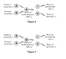
- Demultiplexing is performed on a multiplexed signal light with two optical fibers, to obtain a first signal light (the wavelength is ⁇ S 1 ) and a second signal light (the wavelength is ⁇ S 2 ). Then, two separate wavelength conversions are implemented on the first signal light and the second signal light respectively with two wavelength converters. The wavelength of the first signal light is converted to ⁇ S 2 from ⁇ S 1 and the wavelength of the second signal light is converted to ⁇ S 1 from ⁇ S 2 after the wavelength conversions are implemented. In addition, after each of the wavelength conversions, the converted first signal light and the converted second signal light are filtered out with additional optical filters, and finally multiplexing is performed on the two signal lights on which the information exchange is implemented.
- the signal light with a wavelength of ⁇ S 2 carries the data information once carried by the signal light with an original wavelength of ⁇ S 1
- the signal light with a wavelength of ⁇ S 1 carries the data information once carried by the signal light with an original wavelength of ⁇ S 2 , thereby implementing the all-optical information exchange.
- the conventional technology in the above description has the following defect that the whole process includes multiple optical filtering processes and multiple optical wavelength conversions, and optical components, such as two wavelength converters and four optical filters, are used. Therefore, the system is complex and the cost is high.
- an all-optical information exchange device and an all-optical information exchange method based on the all-optical information exchange device are provided according to the embodiments of the present disclosure.
- the all-optical information exchange device may at least include the following components:
- first port 21 and the second port 22 of the first optical coupler 2 are located on a same side, and the third port 23 and the fourth port 24 are located on the other side.
- first port 31 and the second port 32 of the third optical coupler 3 are located on a same side, and the third port 33 is located on the other side.
- the first port 41 and the second port 42 of the fourth optical coupler 4 are located on a same side, and the third port 43 is located on the other side
- a signal light can not be transmitted between two ports located on a same side, but can be transmitted between two ports located on different sides. Therefore, a signal light can not be transmitted between the first port 21 and the second port 22 of the first optical coupler 2, but can be transmitted between the first port 21 and the third port 23, between the first port 21 and the fourth port 24, between the second port 22 and the third port 23, and between the second port 22 and the fourth port 24.
- a signal light can not be transmitted between the first port 31 and the second port 32 of the third optical coupler 3, but can be transmitted between the third port 33 and the first port 31, and between the third port 33 and the second port 32; a signal light can not be transmitted between the first port 41 and the second port 42 of the fourth optical coupler 4, but can be transmitted between the third port 43 and the first port 41, and between the third port 43 and the second port 42.
- a WDM signal light is input from the first port 21 of the first optical coupler 2 and finally output from the second port 22, and a control light is input from the second port 32 of the third optical coupler 3 and the second port 42 of the fourth optical coupler 4.
- a second optical coupler 8 may be added, as shown in Figure 3 .
- a first port 81 of the second optical coupler 8 is connected to the second port 32 of the third optical coupler 3, and a second port 82 of the second optical coupler 8 is connected to the second port 42 of the fourth optical coupler 4.
- the first port 81 and the second port 82 of the second optical coupler 8 are located on a same side, and a third port 83 is located on the other side. Therefore, a signal light can not be transmitted between the first port 81 and the second port 82, but can be transmitted between the third port 83 and the first port 81 and between the third port 83 and the second port 82.
- the control light can be input from the third port 83, then be output from the first port 81 and the second port 82 respectively, and then input to the second port 32 of the third optical coupler 3 and the second port 42 of the fourth optical coupler 4 respectively.
- the second optical coupler 8 may be a power-equally-divided optical coupler, so that the control light can be equally input to the second port 32 and the second port 42.
- the other optical couplers described above may also be power-equally-divided optical couplers.
- the second-order nonlinear optical waveguide refers to an optical waveguide device with a second-order nonlinear optical effect, and the second-order nonlinear optical effect may be a double-frequency effect, a sum-frequency effect or a difference-frequency effect.
- a wavelength of the signal light is ⁇ S and a wavelength of the control light is ⁇ P
- a polarization state corresponding to the second-order nonlinear optical waveguide, a polarization state of the WDM signal light and a polarization state of the control light are consistent
- the wavelength ⁇ P of the control light is equal to a quasi-phase-matched (QPM) wavelength of the second-order nonlinear optical waveguide.
- QPM quasi-phase-matched
- the signal light ( ⁇ S ) and the control light ( ⁇ P ) transmitted along a same direction are inputted into the second-order nonlinear optical waveguide, and then the signal light ( ⁇ S ) and the control light ( ⁇ P ) experience the second-order nonlinear optical effect in the second-order nonlinear optical waveguide.
- photons of the control light ( ⁇ P ) are annihilated and photons of a double-frequency light ( ⁇ SH ) are generated.
- the photons of the double-frequency light ( ⁇ SH ) are further converted to photons of the signal light ( ⁇ S ) and photons of a generated idle light ( ⁇ i ).
- the first optical coupler 2, the first optical filter 5, the second optical filter 6, the third optical coupler 3 , the second-order nonlinear optical waveguide 1 and the fourth optical coupler 4 described above form an annular structure.
- a WDM signal light is split into two paths and then input into the annular structure under the effect of the first optical coupler 2.
- the two paths of the signal light are transmitted along opposite directions, one of the paths is transmitted along the clockwise direction in the annular structure, and the other of the paths is transmitted along the anti-clockwise direction in the annular structure.
- Two paths of a control light which are input from the second port 32 of the third optical coupler 3 and the second port 42 of the fourth optical coupler 4 are also transmitted along two opposite directions, one of the paths is transmitted along the clockwise direction in the annular structure, and the other of the paths is transmitted along the anti-clockwise direction in the annular structure.
- the WDM signal transmitted along the clockwise direction is input into the first optical filter 5 via the third port 23 of the first optical coupler 2.
- the signal light with the wavelength ⁇ S 1 can pass through the first optical filter 5, thus the signal light with the wavelength ⁇ S 1 is output from the output port 52 of the first optical filter 5.
- a multiplexed light output from the second port 12 of the second-order nonlinear optical waveguide 1 includes the light (the wavelength is A S2 ) which carries the data information and the light with the wavelength ⁇ S 1 .
- the multiplexed light is input from the second port 62 of the second optical filter 6.
- the signal light with the wavelength ⁇ S 2 can pass through the second optical filter 6, thus the signal light with the wavelength ⁇ S 2 is output from the first port 61 of the second optical filter 6 and carries the data information which once carried by the signal light with the wavelength ⁇ S 1 .
- the WDM signal transmitted along the clockwise direction is input into the second optical filter 6 via the fourth port 24 of the first optical coupler 2.
- the signal light with the wavelength ⁇ S 2 can pass through the first optical filter 6, thus the signal light with the wavelength ⁇ S 2 is output from the output port 62 of the second optical filter 6.
- a multiplexed light output from the first port 11 of the second-order nonlinear optical waveguide 1 includes the light (the wavelength is ⁇ S 1 ) which carries the data information and the light with the wavelength ⁇ S 2 .
- the multiplexed light is input from the second port 52 of the first optical filter 5.
- the signal light with the wavelength ⁇ S 1 can pass through the first optical filter 5, thus the signal light with the wavelength ⁇ S 1 is output from the first port 51 of the first optical filter 5 and carries the data information which once carried by the signal light with the wavelength ⁇ S 1 .
- the signal light with the wavelength ⁇ S 2 output from the first port 61 of the second optical filter 6 is input from the third port 23 of the first optical coupler, and the signal light with the wavelength ⁇ S 1 output from the first port 51 of the second optical filter 5 is input from the fourth port 24 of the first optical coupler 2.
- the two signal lights are coupled in the first optical coupler. In this way, the signal light output from the second port 22 is also a multiplexed light, and the all-optical information exchange are implemented on the data information carried by the two optical wavelengths.
- the all-optical information exchange device may be applied to all-optical wavebands exchange, that is, data information carried by a waveband signal light (a waveband includes multiple wavelengths) is copied to another waveband signal light (another waveband includes multiple wavelengths).
- Figure 9 illustrates a process of implementing the controllable all-optical wavebands exchange (dual wavebands) based on the second-order nonlinear optical waveguide.
- the operation principle illustrated in Figure 9 is similar to that in Figure 8 , the difference is that two waveband signal lights are input in the process of the all-optical wavebands exchange.
- One of the wavebands is ⁇ S 1 ... ⁇ SN
- the other of the wavebands is ⁇ ⁇ S 1 ... ⁇ ⁇ SN . All the wavelengths in each of the wavebands are distributed uniformly (or, nonuniformly).
- the frequency of the control light is twice as much as the sum of a center frequency of the first wavelength/waveband signal light and a center frequency of the second wavelength/waveband signal light.
- twice the frequency of the control light may be set to be equal to the sum of a center frequency of the first wavelength/waveband signal light and a center frequency of the second wavelength/waveband signal light.
- the first optical filer 5 and the second optical filter 6 are respectively transmissive to the above two wavebands.
- the first optical filter is transmissive to the signal light with the waveband ⁇ S 1 ... ⁇ SN
- the second optical filter 6 is transmissive to the signal light with the waveband ⁇ ⁇ S 1 ... ⁇ ⁇ SN .
- control light is consistent with polarization states of the two waveband signal lights and is consistent with a corresponding polarization state in which a best nonlinear effect occurs in the second-order nonlinear optical waveguide 1.
- the wavebands ⁇ S 1 ... ⁇ SN can be respectively converted to the wavebands ⁇ ⁇ S 1 ... ⁇ ⁇ SN in the clockwise direction, and the wavebands ⁇ ⁇ S 1 ... ⁇ ⁇ SN . can be respectively converted to the waveband ⁇ S 1 ... ⁇ SN in the anti-clockwise direction.
- the dual waveband signal lights on which the all-optical wavebands exchange is implemented are finally output.
- the QPM wavelength of the second-order nonlinear optical waveguide may be tuned through temperature control.
- the first optical filter 5 and the second optical filter 6 are respectively transmissive to two tunable wavelengths or wavebands.
- temperature control may be implemented on the second-order nonlinear optical waveguide to tune its QPM wavelength, so as to match the wavelength of the control light in a case that the wavelength of the control light changes.
- the controllable all-optical wavelengths or wavebands exchange can be implemented with one second-order nonlinear optical waveguide and two optical filters.
- the process may be carried out for several times.
- the device according to any one of the above embodiments may further include a first optical isolator 9, as shown in Figure 10 .
- the second port 72 of the first polarization controller 7 is connected to the first port 21 of the first optical coupler 2 via the first optical isolator 9: an input port 91 of the first optical isolator 9 is connected to the second port 72 of the first polarization controller 7, and an output port 92 of the first optical isolator is connected to the first port 21 of the first optical coupler 2.
- the device according to any one of the above embodiments may further include a second optical isolator 10, as shown in Figure 11 .
- the device according to any one of the above embodiments may further include a control-light providing device 13, as shown in Figure 12 .
- the control-light providing device 13 is configured to provide the control light.
- the control-light providing device 13 described above may include at least one of a control-light generating device 14 and a second polarization controller 15.
- Figure 13 illustrates a case in which the control-light generating device 14 and the second polarization controller 15 are both provided.
- a first port 151 of the second polarization controller 15 is connected to an output port 141 of the control-light generating device 14, a second port 152 of the second polarization controller 15 is connected to an input port 101 of the second optical isolator 10, and an output port 102 of the second optical isolator 10 is connected to the third port 83 of the second optical coupler 8.
- the polarization state corresponding to the second-order nonlinear optical waveguide 1, the polarization state of the input WDM signal light and the polarization state of the control light are consistent
- the first polarization controller 7 may be configured to adjust the polarization state of inputted WDM signal light
- the second polarization controller 15 may be configured to adjust the polarization state of the control light.
- the polarization state of the input WDM signal light and the polarization state of the control light can be consistent with the polarization state corresponding to the second-order nonlinear optical waveguide 1, by controlling the first polarization controller 7 and the second polarization controller 15.
- the second-order nonlinear optical waveguide 1 may be provided with a polarization controller, in this case, the second polarization controller 15 is not provided.
- an all-optical information exchange method is provided according to the embodiments of the present disclosure, the method is applied to exchanging the data information carried by the first wavelength/waveband signal light and the second wavelength/waveband signal light in the WDM signal light; and the method includes:
- the preset conditions includes: the first optical filter 5 is transmissive to the first wavelength/waveband signal light; the second optical filter 6 is transmissive to the second wavelength/waveband signal light; the polarization state corresponding to the second-order nonlinear optical waveguide 1, the polarization state of the inputted WDM signal light and the polarization state of the control light are consistent; the wavelength of the control light is equal to the quasi-phase-matched wavelength of the second-order nonlinear optical waveguide; and the frequency of the control light is equal to the half of the sum of the center frequency of the first wavelength/waveband signal light and the center frequency of the second wavelength/waveband signal light.
- the second-order nonlinear optical waveguide may be a periodically-poled lithium niobate optical waveguide or other optical waveguide with a second-order nonlinearity.
- the all-optical wavelengths exchange is implemented through a conversion process of an individual one-way wavelength, and the optical components such as two wavelength converters and four optical filters are used, thus the device is complex and the cost is high.
- the all-optical information exchange device a single wavelength converter (i.e., the second-order nonlinear optical waveguide 1) and two optical filters are used, the all-optical wavelengths conversion is implemented by intelligently using the annular structure, and the device is simple, thereby effectively reducing the cost.
- the principle of the wavelength conversion based on the second-order nonlinear optical effect of the second-order nonlinear optical waveguide and the annular structure are combined, only one continuous control light without a high optical power is needed, not only the all-optical wavelengths exchange of the dual wavelengths but also the all-optical wavebands exchange can be implement.
- the implementation is simple, the power consumption is effectively reduced, and the function of the all-optical exchange is improved.
- the all-optical information exchange can be implemented by accordingly tuning the wavelength of the control light and performing the temperature control on the quasi-phase-matched wavelength of the second-order nonlinear optical waveguide, thus the function of the all-optical exchange can be flexibly tunned in the practical applications.
- the components used in the device for all-optical exchange are all passive components, and the exchange is implemented based on the second-order nonlinear effect.
- the device has a property that the response rate is ultrafast (on the order of femtoseconds), thus the device is applicable to the all-optical wavelengths/wavebands exchange with a rate of 40 Gbit/s, 160 Gbit/s, 640 Gbit/s and even an ultrafast rate of Tbit/s.
- the second-order nonlinear optical effect of the second-order nonlinear optical waveguide is used, the conversion process of the two-way wavelengths/wavebands has a property that the up-conversion efficiency and the down-conversion efficiency of the wavelengths are comparable, and the noise is low in the process of the nonlinear interactions, thus the device has a good performance in the all-optical wavelengths/wavebands exchange.
Landscapes
- Physics & Mathematics (AREA)
- Nonlinear Science (AREA)
- General Physics & Mathematics (AREA)
- Optics & Photonics (AREA)
- Engineering & Computer Science (AREA)
- Computer Networks & Wireless Communication (AREA)
- Signal Processing (AREA)
- Electromagnetism (AREA)
- Optical Communication System (AREA)
- Optical Modulation, Optical Deflection, Nonlinear Optics, Optical Demodulation, Optical Logic Elements (AREA)
Applications Claiming Priority (2)
| Application Number | Priority Date | Filing Date | Title |
|---|---|---|---|
| CN201310419699.0A CN104469555B (zh) | 2013-09-13 | 2013-09-13 | 全光信息交换装置及方法 |
| PCT/CN2014/075538 WO2015035775A1 (zh) | 2013-09-13 | 2014-04-16 | 全光信息交换装置及方法 |
Publications (3)
| Publication Number | Publication Date |
|---|---|
| EP3046334A1 true EP3046334A1 (de) | 2016-07-20 |
| EP3046334A4 EP3046334A4 (de) | 2016-08-03 |
| EP3046334B1 EP3046334B1 (de) | 2017-11-15 |
Family
ID=52665007
Family Applications (1)
| Application Number | Title | Priority Date | Filing Date |
|---|---|---|---|
| EP14844392.2A Active EP3046334B1 (de) | 2013-09-13 | 2014-04-16 | Vorrichtung und verfahren für rein optischen informationsaustausch |
Country Status (4)
| Country | Link |
|---|---|
| US (1) | US9618822B2 (de) |
| EP (1) | EP3046334B1 (de) |
| CN (1) | CN104469555B (de) |
| WO (1) | WO2015035775A1 (de) |
Families Citing this family (2)
| Publication number | Priority date | Publication date | Assignee | Title |
|---|---|---|---|---|
| CN116430644A (zh) * | 2023-03-24 | 2023-07-14 | 电子科技大学 | 一种基于周期性极化型铌酸锂晶体的高偏振隔离的光参量放大器 |
| CN118714480A (zh) * | 2023-03-27 | 2024-09-27 | 鹏城实验室 | 一种波长变换系统和波长变换方法 |
Family Cites Families (14)
| Publication number | Priority date | Publication date | Assignee | Title |
|---|---|---|---|---|
| JP4454763B2 (ja) * | 2000-03-03 | 2010-04-21 | 富士通株式会社 | 信号光を波形整形するための方法、装置及びシステム |
| CN1194453C (zh) * | 2001-09-13 | 2005-03-23 | 华为技术有限公司 | 一种多波长输出光纤激光器 |
| CN1308765C (zh) * | 2003-08-29 | 2007-04-04 | 华中科技大学 | 差频型全光波长转换器 |
| JP4043463B2 (ja) * | 2004-09-02 | 2008-02-06 | 沖電気工業株式会社 | 光スイッチ |
| KR100658532B1 (ko) * | 2004-12-02 | 2006-12-15 | 한국과학기술연구원 | 가변 다채널 필터 |
| CN101303507B (zh) | 2006-12-01 | 2011-04-20 | 华中科技大学 | 一种基于铌酸锂光波导环形腔的全光波长转换装置 |
| JP4467557B2 (ja) * | 2006-12-25 | 2010-05-26 | 富士通株式会社 | 光スイッチング方法及び光スイッチ |
| CN100442136C (zh) * | 2006-12-28 | 2008-12-10 | 华中科技大学 | 一种非归零码到归零码全光码型转换装置 |
| JP4683099B2 (ja) * | 2008-09-16 | 2011-05-11 | 沖電気工業株式会社 | 光多値変調信号発生装置 |
| JP2010206289A (ja) * | 2009-02-27 | 2010-09-16 | Fujitsu Ltd | 光信号処理装置及び方法 |
| CN101989024B (zh) * | 2009-07-31 | 2013-04-17 | 华中科技大学 | 一种光信号的传输方法及装置 |
| CN102547492B (zh) * | 2011-12-17 | 2014-06-04 | 华中科技大学 | 一种基于二阶非线性的全光信息交换方法 |
| CN102931567B (zh) * | 2012-11-01 | 2015-05-13 | 贵州大学 | 全光微波信号振荡器 |
| JP6079192B2 (ja) * | 2012-12-11 | 2017-02-15 | 富士通株式会社 | 光周波数多重装置及び偏光制御方法 |
-
2013
- 2013-09-13 CN CN201310419699.0A patent/CN104469555B/zh active Active
-
2014
- 2014-04-16 WO PCT/CN2014/075538 patent/WO2015035775A1/zh not_active Ceased
- 2014-04-16 EP EP14844392.2A patent/EP3046334B1/de active Active
-
2016
- 2016-03-11 US US15/068,158 patent/US9618822B2/en active Active
Also Published As
| Publication number | Publication date |
|---|---|
| WO2015035775A1 (zh) | 2015-03-19 |
| CN104469555A (zh) | 2015-03-25 |
| CN104469555B (zh) | 2018-05-18 |
| US9618822B2 (en) | 2017-04-11 |
| US20160195792A1 (en) | 2016-07-07 |
| EP3046334B1 (de) | 2017-11-15 |
| EP3046334A4 (de) | 2016-08-03 |
Similar Documents
| Publication | Publication Date | Title |
|---|---|---|
| Xie et al. | Programmable optical processor chips: toward photonic RF filters with DSP-level flexibility and MHz-band selectivity | |
| CN102608824B (zh) | 基于相位调制器的可调谐光学变频器 | |
| CN101303507B (zh) | 一种基于铌酸锂光波导环形腔的全光波长转换装置 | |
| Lei et al. | All-optical canonical logic units-based programmable logic array (CLUs-PLA) using semiconductor optical amplifiers | |
| US10591804B2 (en) | Quantum wave-converter | |
| US9618822B2 (en) | Device and method for all-optical information exchange | |
| WO2013075566A1 (zh) | 基于幅度调制器的可调谐光学变频器 | |
| Li et al. | Reconfigurable Microwave Photonic Filters with Ultrasteep Roll‐Off Based on Optical Microcombs | |
| Chen et al. | Chip‐Scale Dispersion Compensation of High‐Speed Data–Recent Progress and Future Perspectives | |
| CN117031630A (zh) | 一种幺正光学路径模式转换器及转换方法 | |
| CN110596819B (zh) | 基于微环谐振器的窄带光滤波器 | |
| CN113031164B (zh) | 光滤波器结构和光学滤波器 | |
| Fisher et al. | Integrated optical device for frequency conversion across the full telecom c-band spectrum | |
| US20030193710A1 (en) | Method and apparatus for generating a sequence of optical wavelength bands | |
| CN110187587B (zh) | 一种基于npr等效可饱和吸收体的光量化装置及方法 | |
| EP4692922A1 (de) | Wellenlängenumwandlungssystem und wellenlängenumwandlungsverfahren | |
| CN113253538A (zh) | 基于马赫曾德尔干涉仪宽率调谐路径纠缠和频率纠缠芯片 | |
| Moss | Ultra-high performance microwave spectral filters using optical microcombs | |
| Furukawa et al. | Tunable all-optical wavelength conversion of 160 Gbit/s RZ signals based on cascaded SFG-DFG in PPLN waveguide | |
| Cugini et al. | Flexible transceivers and solutions for semi-filterless metro networks | |
| Moss | Microwave spectral filters with ultra sharp rolloff bands based on optical microcombs | |
| Ismail et al. | Performance evaluation of wavelength exchanging in optical interconnect | |
| Moss | Ultra-high performance microwave photonic spectral filters based on microcombs | |
| CN1971394A (zh) | 基于铌酸锂光波导环形腔的全光波长转换装置 | |
| Moss | Microwave photonic spectral filters with ultra sharp rolloff bands based on microcombs |
Legal Events
| Date | Code | Title | Description |
|---|---|---|---|
| PUAI | Public reference made under article 153(3) epc to a published international application that has entered the european phase |
Free format text: ORIGINAL CODE: 0009012 |
|
| 17P | Request for examination filed |
Effective date: 20160324 |
|
| AK | Designated contracting states |
Kind code of ref document: A1 Designated state(s): AL AT BE BG CH CY CZ DE DK EE ES FI FR GB GR HR HU IE IS IT LI LT LU LV MC MK MT NL NO PL PT RO RS SE SI SK SM TR |
|
| AX | Request for extension of the european patent |
Extension state: BA ME |
|
| A4 | Supplementary search report drawn up and despatched |
Effective date: 20160701 |
|
| RIC1 | Information provided on ipc code assigned before grant |
Ipc: H04Q 11/00 20060101AFI20160627BHEP Ipc: G02F 1/35 20060101ALI20160627BHEP Ipc: G02F 2/00 20060101ALI20160627BHEP |
|
| DAX | Request for extension of the european patent (deleted) | ||
| RIC1 | Information provided on ipc code assigned before grant |
Ipc: G02F 1/35 20060101ALI20170428BHEP Ipc: G02F 2/00 20060101ALI20170428BHEP Ipc: H04Q 11/00 20060101AFI20170428BHEP |
|
| GRAP | Despatch of communication of intention to grant a patent |
Free format text: ORIGINAL CODE: EPIDOSNIGR1 |
|
| STAA | Information on the status of an ep patent application or granted ep patent |
Free format text: STATUS: GRANT OF PATENT IS INTENDED |
|
| INTG | Intention to grant announced |
Effective date: 20170612 |
|
| GRAS | Grant fee paid |
Free format text: ORIGINAL CODE: EPIDOSNIGR3 |
|
| GRAA | (expected) grant |
Free format text: ORIGINAL CODE: 0009210 |
|
| STAA | Information on the status of an ep patent application or granted ep patent |
Free format text: STATUS: THE PATENT HAS BEEN GRANTED |
|
| AK | Designated contracting states |
Kind code of ref document: B1 Designated state(s): AL AT BE BG CH CY CZ DE DK EE ES FI FR GB GR HR HU IE IS IT LI LT LU LV MC MK MT NL NO PL PT RO RS SE SI SK SM TR |
|
| REG | Reference to a national code |
Ref country code: CH Ref legal event code: EP Ref country code: GB Ref legal event code: FG4D Ref country code: AT Ref legal event code: REF Ref document number: 947373 Country of ref document: AT Kind code of ref document: T Effective date: 20171115 |
|
| REG | Reference to a national code |
Ref country code: IE Ref legal event code: FG4D |
|
| REG | Reference to a national code |
Ref country code: DE Ref legal event code: R096 Ref document number: 602014017418 Country of ref document: DE |
|
| REG | Reference to a national code |
Ref country code: NL Ref legal event code: MP Effective date: 20171115 |
|
| REG | Reference to a national code |
Ref country code: LT Ref legal event code: MG4D |
|
| REG | Reference to a national code |
Ref country code: AT Ref legal event code: MK05 Ref document number: 947373 Country of ref document: AT Kind code of ref document: T Effective date: 20171115 |
|
| PG25 | Lapsed in a contracting state [announced via postgrant information from national office to epo] |
Ref country code: FI Free format text: LAPSE BECAUSE OF FAILURE TO SUBMIT A TRANSLATION OF THE DESCRIPTION OR TO PAY THE FEE WITHIN THE PRESCRIBED TIME-LIMIT Effective date: 20171115 Ref country code: ES Free format text: LAPSE BECAUSE OF FAILURE TO SUBMIT A TRANSLATION OF THE DESCRIPTION OR TO PAY THE FEE WITHIN THE PRESCRIBED TIME-LIMIT Effective date: 20171115 Ref country code: SE Free format text: LAPSE BECAUSE OF FAILURE TO SUBMIT A TRANSLATION OF THE DESCRIPTION OR TO PAY THE FEE WITHIN THE PRESCRIBED TIME-LIMIT Effective date: 20171115 Ref country code: LT Free format text: LAPSE BECAUSE OF FAILURE TO SUBMIT A TRANSLATION OF THE DESCRIPTION OR TO PAY THE FEE WITHIN THE PRESCRIBED TIME-LIMIT Effective date: 20171115 Ref country code: NL Free format text: LAPSE BECAUSE OF FAILURE TO SUBMIT A TRANSLATION OF THE DESCRIPTION OR TO PAY THE FEE WITHIN THE PRESCRIBED TIME-LIMIT Effective date: 20171115 Ref country code: NO Free format text: LAPSE BECAUSE OF FAILURE TO SUBMIT A TRANSLATION OF THE DESCRIPTION OR TO PAY THE FEE WITHIN THE PRESCRIBED TIME-LIMIT Effective date: 20180215 |
|
| PG25 | Lapsed in a contracting state [announced via postgrant information from national office to epo] |
Ref country code: LV Free format text: LAPSE BECAUSE OF FAILURE TO SUBMIT A TRANSLATION OF THE DESCRIPTION OR TO PAY THE FEE WITHIN THE PRESCRIBED TIME-LIMIT Effective date: 20171115 Ref country code: BG Free format text: LAPSE BECAUSE OF FAILURE TO SUBMIT A TRANSLATION OF THE DESCRIPTION OR TO PAY THE FEE WITHIN THE PRESCRIBED TIME-LIMIT Effective date: 20180215 Ref country code: RS Free format text: LAPSE BECAUSE OF FAILURE TO SUBMIT A TRANSLATION OF THE DESCRIPTION OR TO PAY THE FEE WITHIN THE PRESCRIBED TIME-LIMIT Effective date: 20171115 Ref country code: GR Free format text: LAPSE BECAUSE OF FAILURE TO SUBMIT A TRANSLATION OF THE DESCRIPTION OR TO PAY THE FEE WITHIN THE PRESCRIBED TIME-LIMIT Effective date: 20180216 Ref country code: AT Free format text: LAPSE BECAUSE OF FAILURE TO SUBMIT A TRANSLATION OF THE DESCRIPTION OR TO PAY THE FEE WITHIN THE PRESCRIBED TIME-LIMIT Effective date: 20171115 Ref country code: HR Free format text: LAPSE BECAUSE OF FAILURE TO SUBMIT A TRANSLATION OF THE DESCRIPTION OR TO PAY THE FEE WITHIN THE PRESCRIBED TIME-LIMIT Effective date: 20171115 |
|
| PG25 | Lapsed in a contracting state [announced via postgrant information from national office to epo] |
Ref country code: CZ Free format text: LAPSE BECAUSE OF FAILURE TO SUBMIT A TRANSLATION OF THE DESCRIPTION OR TO PAY THE FEE WITHIN THE PRESCRIBED TIME-LIMIT Effective date: 20171115 Ref country code: EE Free format text: LAPSE BECAUSE OF FAILURE TO SUBMIT A TRANSLATION OF THE DESCRIPTION OR TO PAY THE FEE WITHIN THE PRESCRIBED TIME-LIMIT Effective date: 20171115 Ref country code: CY Free format text: LAPSE BECAUSE OF FAILURE TO SUBMIT A TRANSLATION OF THE DESCRIPTION OR TO PAY THE FEE WITHIN THE PRESCRIBED TIME-LIMIT Effective date: 20171115 Ref country code: DK Free format text: LAPSE BECAUSE OF FAILURE TO SUBMIT A TRANSLATION OF THE DESCRIPTION OR TO PAY THE FEE WITHIN THE PRESCRIBED TIME-LIMIT Effective date: 20171115 Ref country code: SK Free format text: LAPSE BECAUSE OF FAILURE TO SUBMIT A TRANSLATION OF THE DESCRIPTION OR TO PAY THE FEE WITHIN THE PRESCRIBED TIME-LIMIT Effective date: 20171115 |
|
| REG | Reference to a national code |
Ref country code: DE Ref legal event code: R097 Ref document number: 602014017418 Country of ref document: DE |
|
| PG25 | Lapsed in a contracting state [announced via postgrant information from national office to epo] |
Ref country code: SM Free format text: LAPSE BECAUSE OF FAILURE TO SUBMIT A TRANSLATION OF THE DESCRIPTION OR TO PAY THE FEE WITHIN THE PRESCRIBED TIME-LIMIT Effective date: 20171115 Ref country code: IT Free format text: LAPSE BECAUSE OF FAILURE TO SUBMIT A TRANSLATION OF THE DESCRIPTION OR TO PAY THE FEE WITHIN THE PRESCRIBED TIME-LIMIT Effective date: 20171115 Ref country code: RO Free format text: LAPSE BECAUSE OF FAILURE TO SUBMIT A TRANSLATION OF THE DESCRIPTION OR TO PAY THE FEE WITHIN THE PRESCRIBED TIME-LIMIT Effective date: 20171115 Ref country code: PL Free format text: LAPSE BECAUSE OF FAILURE TO SUBMIT A TRANSLATION OF THE DESCRIPTION OR TO PAY THE FEE WITHIN THE PRESCRIBED TIME-LIMIT Effective date: 20171115 |
|
| PLBE | No opposition filed within time limit |
Free format text: ORIGINAL CODE: 0009261 |
|
| STAA | Information on the status of an ep patent application or granted ep patent |
Free format text: STATUS: NO OPPOSITION FILED WITHIN TIME LIMIT |
|
| 26N | No opposition filed |
Effective date: 20180817 |
|
| PG25 | Lapsed in a contracting state [announced via postgrant information from national office to epo] |
Ref country code: SI Free format text: LAPSE BECAUSE OF FAILURE TO SUBMIT A TRANSLATION OF THE DESCRIPTION OR TO PAY THE FEE WITHIN THE PRESCRIBED TIME-LIMIT Effective date: 20171115 Ref country code: MC Free format text: LAPSE BECAUSE OF FAILURE TO SUBMIT A TRANSLATION OF THE DESCRIPTION OR TO PAY THE FEE WITHIN THE PRESCRIBED TIME-LIMIT Effective date: 20171115 |
|
| REG | Reference to a national code |
Ref country code: CH Ref legal event code: PL |
|
| REG | Reference to a national code |
Ref country code: BE Ref legal event code: MM Effective date: 20180430 |
|
| REG | Reference to a national code |
Ref country code: IE Ref legal event code: MM4A |
|
| PG25 | Lapsed in a contracting state [announced via postgrant information from national office to epo] |
Ref country code: LU Free format text: LAPSE BECAUSE OF NON-PAYMENT OF DUE FEES Effective date: 20180416 |
|
| PG25 | Lapsed in a contracting state [announced via postgrant information from national office to epo] |
Ref country code: CH Free format text: LAPSE BECAUSE OF NON-PAYMENT OF DUE FEES Effective date: 20180430 Ref country code: LI Free format text: LAPSE BECAUSE OF NON-PAYMENT OF DUE FEES Effective date: 20180430 Ref country code: BE Free format text: LAPSE BECAUSE OF NON-PAYMENT OF DUE FEES Effective date: 20180430 |
|
| PG25 | Lapsed in a contracting state [announced via postgrant information from national office to epo] |
Ref country code: IE Free format text: LAPSE BECAUSE OF NON-PAYMENT OF DUE FEES Effective date: 20180416 Ref country code: FR Free format text: LAPSE BECAUSE OF NON-PAYMENT OF DUE FEES Effective date: 20180430 |
|
| PG25 | Lapsed in a contracting state [announced via postgrant information from national office to epo] |
Ref country code: MT Free format text: LAPSE BECAUSE OF NON-PAYMENT OF DUE FEES Effective date: 20180416 |
|
| PG25 | Lapsed in a contracting state [announced via postgrant information from national office to epo] |
Ref country code: TR Free format text: LAPSE BECAUSE OF FAILURE TO SUBMIT A TRANSLATION OF THE DESCRIPTION OR TO PAY THE FEE WITHIN THE PRESCRIBED TIME-LIMIT Effective date: 20171115 |
|
| PG25 | Lapsed in a contracting state [announced via postgrant information from national office to epo] |
Ref country code: PT Free format text: LAPSE BECAUSE OF FAILURE TO SUBMIT A TRANSLATION OF THE DESCRIPTION OR TO PAY THE FEE WITHIN THE PRESCRIBED TIME-LIMIT Effective date: 20171115 |
|
| PG25 | Lapsed in a contracting state [announced via postgrant information from national office to epo] |
Ref country code: HU Free format text: LAPSE BECAUSE OF FAILURE TO SUBMIT A TRANSLATION OF THE DESCRIPTION OR TO PAY THE FEE WITHIN THE PRESCRIBED TIME-LIMIT; INVALID AB INITIO Effective date: 20140416 Ref country code: MK Free format text: LAPSE BECAUSE OF NON-PAYMENT OF DUE FEES Effective date: 20171115 |
|
| PG25 | Lapsed in a contracting state [announced via postgrant information from national office to epo] |
Ref country code: AL Free format text: LAPSE BECAUSE OF FAILURE TO SUBMIT A TRANSLATION OF THE DESCRIPTION OR TO PAY THE FEE WITHIN THE PRESCRIBED TIME-LIMIT Effective date: 20171115 Ref country code: IS Free format text: LAPSE BECAUSE OF FAILURE TO SUBMIT A TRANSLATION OF THE DESCRIPTION OR TO PAY THE FEE WITHIN THE PRESCRIBED TIME-LIMIT Effective date: 20180315 |
|
| P01 | Opt-out of the competence of the unified patent court (upc) registered |
Effective date: 20230524 |
|
| PGFP | Annual fee paid to national office [announced via postgrant information from national office to epo] |
Ref country code: DE Payment date: 20250305 Year of fee payment: 12 |
|
| PGFP | Annual fee paid to national office [announced via postgrant information from national office to epo] |
Ref country code: GB Payment date: 20260310 Year of fee payment: 13 |