EP3048669A1 - Aus platten geformte antenne und verfahren zur herstellung - Google Patents
Aus platten geformte antenne und verfahren zur herstellung Download PDFInfo
- Publication number
- EP3048669A1 EP3048669A1 EP16151280.1A EP16151280A EP3048669A1 EP 3048669 A1 EP3048669 A1 EP 3048669A1 EP 16151280 A EP16151280 A EP 16151280A EP 3048669 A1 EP3048669 A1 EP 3048669A1
- Authority
- EP
- European Patent Office
- Prior art keywords
- plane
- splitter
- feeding network
- splitters
- plate
- Prior art date
- Legal status (The legal status is an assumption and is not a legal conclusion. Google has not performed a legal analysis and makes no representation as to the accuracy of the status listed.)
- Granted
Links
Images



Classifications
-
- H—ELECTRICITY
- H01—ELECTRIC ELEMENTS
- H01P—WAVEGUIDES; RESONATORS, LINES, OR OTHER DEVICES OF THE WAVEGUIDE TYPE
- H01P5/00—Coupling devices of the waveguide type
- H01P5/12—Coupling devices having more than two ports
- H01P5/16—Conjugate devices, i.e. devices having at least one port decoupled from one other port
- H01P5/19—Conjugate devices, i.e. devices having at least one port decoupled from one other port of the junction type
-
- H—ELECTRICITY
- H01—ELECTRIC ELEMENTS
- H01Q—ANTENNAS, i.e. RADIO AERIALS
- H01Q21/00—Antenna arrays or systems
- H01Q21/0006—Particular feeding systems
- H01Q21/0025—Modular arrays
-
- H—ELECTRICITY
- H01—ELECTRIC ELEMENTS
- H01Q—ANTENNAS, i.e. RADIO AERIALS
- H01Q21/00—Antenna arrays or systems
- H01Q21/06—Arrays of individually energised antenna units similarly polarised and spaced apart
- H01Q21/061—Two dimensional planar arrays
- H01Q21/064—Two dimensional planar arrays using horn or slot aerials
Definitions
- the present invention relates generally to antennae and more particularly to antenna arrays.
- Certain embodiments of the present invention seek to provide an antenna array configuration with h-plane splitters between ends of a feeding network and radiating elements e.g. horns, thereby to reduce the distance between the centers of the horns to less than one wavelength which results in a better side lobe level.
- Certain embodiments of the present invention seek to manufacture upper and lower plates together constituting an antenna, typically each plate in a single operation, by dividing the feeding network's waveguides at the centre where there are no cross currents so as not to disturb propagation in the feeding network.
- An advantage of certain embodiments is that propagation in the feeding network remains undisturbed even if the two halves of the waveguides are not touching each other and instead are bonded to one another, generating a non-zero gap there between.
- the two plates of the antenna may be attached to one another only by screws, rather than soldering the plates together.
- the radiating elements, h-plane splitters and upper half of the feeding network are fabricated in one plate without undercuts hence simplifying manufacture of the plate which may for example be formed using a simple molding machine or a 3 axis-CNC machine. Parts with undercuts require an extra part for the mold and increase the cost of the molded part.
- the waveguide sections need not be uniform in length; for example, the lengths of the waveguide sections may be set to generate beam tilt as is known in the art.
- an element or feature may exist is intended to include (a) embodiments in which the element or feature exists; (b) embodiments in which the element or feature does not exist; and (c) embodiments in which the element or feature exist selectably e.g. a user may configure or select whether the element or feature does or does not exist.
- black lines may denote transition between conductive substrates and empty spaces.
- Fig. 1a depicts currents along the walls of a waveguide, generated by an electromagnetic wave travelling along the waveguide. Each arrow represents the direction of current;
- Figs. 3b - 7b illustrates antenna construction according to certain embodiments of the present invention.
- the antenna typically comprises two plates 10 and 20, lower and upper.
- the lower plate includes the lower half of the waveguides (110) of the feeding network and the upper plate includes radiating elements 30, H-plane splitters 40, and the upper half of the waveguides (120) of the feeding network.
- each feeding network output (100) connects to only two radiating elements and generally, the above three elements (30,40, and 120), in the upper plate, are designed so as not to contain undercuts to facilitate manufacturing in a single plate using a simple molding machine or a 3-axis CNC machine.
- the two machined plates are typically suitably bonded.
- exactly half of a waveguide is formed from one plate and the other half is formed from another plate.
- the division into halves is obtained by bisecting the longer waveguide dimension "a".
- a particular advantage of manufacturing exactly half of the waveguide from one plate and the other half from another plate, where the division into halves is obtained by bisecting the longer waveguide dimension, is that the division-line 130 does not cross any currents as is apparent e.g. from fig. 1a ; it does not disturb the wave's progress along the waveguide, because the currents adjacent to the division-line are parallel to the wave propagation direction hence to the division-line. Therefore the two plates need not be soldered to one another (since it is not necessary to ensure that the separation between the 2 plates be zero). Instead, the two plates may, for example, simply be screwed together, despite the resulting 0.1 mm (say) separation between the plates (e.g. as indicated by the screw-holes 77 shown in Fig.
- Other bonding methods may be welding, soldering, and Laser bonding. This is advantageous e.g. because soldering may be more costly relative to screws, hence its elimination reduces the per-piece manufacturing cost of the antenna. In addition welding or soldering could cause distortion in the plates due to heating effects.
- an antenna array for transmitting/ receiving electromagnetic radiation defining a wavelength comprising:
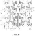
- An E-orientation feeding network layer 60 may comprise:
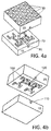
- a lower plate 10 e.g. as shown in Figs. 4a - 4b , exactly two machined plates are provided: a lower plate 10, and a single upper plate 20. Radiating elements 30, H-plane splitters 40 and the top half 120 of the feeding network 60 are included in the upper plate 20, and the bottom half 110 of the feeding network 60 (waveguide sections 70 and E-plane splitters 90) are included in the lower plate 10.
- a lower plate 10 e.g. as shown in Figs. 4a - 4b .
- the antenna includes a total of three machined plates (lower, middle, top-most).
- the lower plate 20 includes half of the feeding network 60 as in the single-upper-plate embodiment
- the middle plate 21 includes half of the feeding network 60 and a bottom half of the h-plane splitter layer
- the top-most plate 22 includes a top-half of the h-plane splitters and the radiating element layer.
- the orientation of the waveguides of the feeding network 60 typically comprises an "E-plane orientation" in which the short cross sectional dimension of the rectangular waveguide 70 parallel to the feeding network plane.
- E-plane orientation for the waveguides of the feeding network 60 may yield one or more of the following advantages:
- a particular advantage of certain embodiments is use of 1 to 2 splitters between the feeding network 60 and the radiating elements 30 instead of 1 to 4 splitters e.g. as in US prior art patent applications US20130120205 and US20130321229 .
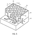
- the advantage of using 1 to 2 splitters is that 1 to 2 splitters with the radiating elements and the upper side of the feeding network does not contain undercuts so it can easily be manufactured in one plate, e.g. as shown in Figs. 5 , 6a .
- 1 to 4 splitters with the radiating elements and the upper side of the feeding network contain undercuts which are difficult to produce in one plate.
- a particular advantage of certain embodiments is offsetting the connection point between the last-level E-plane splitters 95 to the feeding network output 100, referenced 's' in Fig. 3 . As apparent from Fig. 3 this offset directly affects the wall thickness t. As s diminishes, the feeding network outputs 100 moves upwards thus 't' become smaller. When's' is zero, e.g. as in US prior art patent US4743915 , the wall thickness 't' become so small that manufacturing becomes difficult.
- the feeding network 60 of Fig. 3 overcomes the problem of E-plane splitters undesirably inverting the phase of the wave at one of the plural E-plane splitter 90 outputs.
- the electric field direction is represented by the arrow's orientation and phase is represented by the arrow-heads.
- all the outputs of the feeding network 100 (those which connect to the H-plane splitters) are in phase.
- the arrows respectively representing the electric fields at four feeding network outputs 100 all point to the left, although this is not intended to be limiting.
- the electric field direction and phase of the all other outputs 100 are identical to those four outputs.
- Fig. 3 is therefore not necessarily to scale.
- a particular advantage of the above embodiment is that the distance between adjacent elements is of less than one wavelength.
- some or even all of the e-plane splitters may split the power unequally such that one output gets more than half of the power in the splitter input, and the second output get less than half of the input power.
- some or even all of the e-plane splitters may split the power equally such that one output gets exactly half of the power.
- the H-plane splitters e.g. as shown in figs 2b , 6a , typically have one input and two outputs. Each output 100 of the feeding network 60 is connected to an input 45 of H-plane splitter 40.
- any suitable conventional H-plane splitter configuration may be employed.
- an H-plane splitter 40 is connected to each output 100 of the feeding network 60.
- the outputs 50 of the H-plane splitter 40 connect to a pair of radiating elements 30.
- a radiating element 30 (e.g. horn e.g. as shown in figs 4a , 5 , 6a , 7a ) is provided to connect to every output 50 of the H-plane splitters. Any suitable number of radiating elements 30 may be employed e.g. between 4 and 100000.
- each radiating element 30 has one input and one output.
- the input of each radiating element is connected to the output of an H-plane splitter.
- the output of the radiating element 30 radiates the wave into space.
- the distances D1 and D2 ( Fig. 5 ) between each two adjacent radiating elements 30 along the two dimensions of the array of radiating elements respectively, are each typically less than one wavelength in order to reduce side lobes levels and avoid high side lobes. This is achievable e.g. due to the design and dimensions of the feeding network 60 as shown herein and/or due to presence of H-plane splitters between the outputs of the feeding network 60 and the radiating elements 30 e.g. horns.
- the radiating elements 30 may have any suitable configuration: horn (tapered), box horn, rectangular and may have the same dimension as the h-plane splitter output 50 such that the surfaces of the H-plane splitter 40 and radiating elements are continuous.
- a, b are the dimensions of the waveguide's cross-section.
- b 0.26*a or a value closer to 0.25*a than to 0.5*a, to save space.
- this is not intended to be limiting.
- b 0.5*a or even 0.6*a or 0.7*a might be appropriate ratios e.g. at longer wavelengths.
- b might be even less than 0.26*a e.g. 0.1*a.
- the spacing L1 between vertically adjacent elements 30 in Fig. 3 is less than one wavelength.
- L1 is drawn as the distance between corresponding locations in vertically adjacent elements 30.
- the spacing L2 between horizontally adjacent elements 30 in Fig. 3 is less than 2 wavelengths.
- L2 is drawn as the distance between corresponding locations in horizontally adjacent elements 30.
- the waveguide 70 walls are shown schematically as straight.
- the short dimension, b, of the waveguides shown in Fig. 3 may vary along the waveguide, e.g. in the region where the waveguide 70 connects to the E-plane splitters. It is appreciated that the curvature of the e-plane splitters, as well as the waveguide 70 cross-sectional dimensions a, b are not intended to be limiting.
- the output 100 of the feeding network may include a slanted surface 65 at its bottom, to facilitate passage of the wave from feeding network output 100 to h-plane splitter input 45.
- an antenna may include a bottom plate, a middle plate and a top-most plate.
- the radiating element layer is included in the top-most plate; the first and second portions of the H-plane splitter layer are included in the middle and top-most plates respectively; the hollow rectangular waveguide's first and second halves are included in the middle and lower plates respectively; and each E-plane splitter's first and second halves are included in the middle and lower plates respectively.
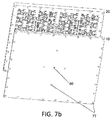
- 7a - 7b includes 2 plates, 1024 radiating elements 30, 512 H-plane splitters, 511 E-plane splitters and a waveguide section 70 intermediate to each E-plane splitter's output and the following E-plane splitter 90 input.
- this is not intended to be limiting.
- any suitable number of radiating elements 30 may be used, even as few as 4 such elements.
- the antenna is symmetric such that the length of the path that the wave travels from the feeding network input 80 to any one of the outputs 100 is always identical, hence the phases of the wave on each of the outputs are identical, although this is not intended to be limiting.
- the waveguide section lengths may be changed to yield beam tilt, as is known in the art.
- the E-plane splitters are arranged to form a parallel feeding network having a binary tree form.
- 512 H-plane splitters may be connected to 256 E-plane splitters which may respectively be connected to 128 E-plane splitters which may respectively be connected to 64 E-plane splitters which may respectively be connected to 32 E-plane splitters which may respectively be connected to 16 E-plane splitters which may respectively be connected to 8 E-plane splitters which may respectively be connected to 4 E-plane splitters which may respectively be connected to 2 E-plane splitters which may respectively be connected to a single E-plane splitter 90 connected directly to the antenna input (e.g. 80 in Fig. 7b ).
- the binary tree need not be "full” e.g. it is possible that one of the outputs of a certain E-plane splitter 90 is split further by a next-level E-splitter, and the other output is not split.
- the number of radiating elements 30 does not have to be a power of 2.
- the scope of the present invention is not limited to structures and functions specifically described herein and is also intended to include devices which have the capacity to yield a structure, or perform a function, described herein, such that even though users of the device may not use the capacity, they are if they so desire able to modify the device to obtain the structure or function.
Landscapes
- Variable-Direction Aerials And Aerial Arrays (AREA)
Applications Claiming Priority (1)
| Application Number | Priority Date | Filing Date | Title |
|---|---|---|---|
| IL236739A IL236739B (en) | 2015-01-15 | 2015-01-15 | Antenna formed from plates and methods useful in conjunction therewith |
Publications (2)
| Publication Number | Publication Date |
|---|---|
| EP3048669A1 true EP3048669A1 (de) | 2016-07-27 |
| EP3048669B1 EP3048669B1 (de) | 2017-07-19 |
Family
ID=55129756
Family Applications (1)
| Application Number | Title | Priority Date | Filing Date |
|---|---|---|---|
| EP16151280.1A Active EP3048669B1 (de) | 2015-01-15 | 2016-01-14 | Aus platten geformte antenne und verfahren zur herstellung |
Country Status (4)
| Country | Link |
|---|---|
| US (2) | US9899722B2 (de) |
| EP (1) | EP3048669B1 (de) |
| ES (1) | ES2643546T3 (de) |
| IL (1) | IL236739B (de) |
Families Citing this family (20)
| Publication number | Priority date | Publication date | Assignee | Title |
|---|---|---|---|---|
| KR102302466B1 (ko) * | 2014-11-11 | 2021-09-16 | 주식회사 케이엠더블유 | 도파관 슬롯 어레이 안테나 |
| US10224617B2 (en) * | 2016-07-26 | 2019-03-05 | Waymo Llc | Plated, injection molded, automotive radar waveguide antenna |
| CN107342454B (zh) * | 2017-06-09 | 2020-02-21 | 宁波大学 | 一种波导缝隙阵列天线 |
| CN111883921B (zh) * | 2020-08-04 | 2023-02-17 | 南京理工大学 | 一种宽带宽波束介质填充喇叭天线 |
| CN112186340B (zh) * | 2020-09-29 | 2023-11-07 | 京东方科技集团股份有限公司 | 天线及其制作方法 |
| US11749883B2 (en) | 2020-12-18 | 2023-09-05 | Aptiv Technologies Limited | Waveguide with radiation slots and parasitic elements for asymmetrical coverage |
| US11901601B2 (en) | 2020-12-18 | 2024-02-13 | Aptiv Technologies Limited | Waveguide with a zigzag for suppressing grating lobes |
| US12058804B2 (en) | 2021-02-09 | 2024-08-06 | Aptiv Technologies AG | Formed waveguide antennas of a radar assembly |
| US11962085B2 (en) | 2021-05-13 | 2024-04-16 | Aptiv Technologies AG | Two-part folded waveguide having a sinusoidal shape channel including horn shape radiating slots formed therein which are spaced apart by one-half wavelength |
| US11616282B2 (en) | 2021-08-03 | 2023-03-28 | Aptiv Technologies Limited | Transition between a single-ended port and differential ports having stubs that match with input impedances of the single-ended and differential ports |
| CN118077103A (zh) * | 2021-10-27 | 2024-05-24 | 华为技术有限公司 | 喇叭天线设备 |
| US12456816B2 (en) | 2022-05-02 | 2025-10-28 | Aptiv Technologies AG | Waveguide with slot antennas and reflectors |
| CN115117616B (zh) * | 2022-08-25 | 2022-12-02 | 成都国恒空间技术工程股份有限公司 | 一种基于rgw结构的victs天线 |
| KR102762064B1 (ko) * | 2022-10-19 | 2025-02-05 | 주식회사 에이치제이웨이브 | 빔 틸트 안테나 |
| KR102821715B1 (ko) * | 2022-10-20 | 2025-06-18 | 주식회사 에이치제이웨이브 | 빔 틸트 안테나 |
| DE102023200363A1 (de) * | 2023-01-18 | 2024-07-18 | Robert Bosch Gesellschaft mit beschränkter Haftung | Leistungsteilungsvorrichtung, Wellenleiterantenne und Verfahren zum Herstellen einer Leistungsteilungvorrichtung |
| US12537308B2 (en) * | 2023-01-24 | 2026-01-27 | Aptiv Technologies AG | Symmetrical two-piece waveguide |
| US12148992B2 (en) | 2023-01-25 | 2024-11-19 | Aptiv Technologies AG | Hybrid horn waveguide antenna |
| US12627020B2 (en) | 2023-05-18 | 2026-05-12 | Aptiv Technologies AG | Waveguide with a curved-wall low-pass filter |
| US12355149B1 (en) * | 2023-06-06 | 2025-07-08 | Utah State University Space Dynamics Laboratory | Waveguide horn antenna |
Citations (12)
| Publication number | Priority date | Publication date | Assignee | Title |
|---|---|---|---|---|
| US4743915A (en) | 1985-06-04 | 1988-05-10 | U.S. Philips Corporation | Four-horn radiating modules with integral power divider/supply network |
| US4783663A (en) | 1985-06-04 | 1988-11-08 | U.S. Philips Corporation | Unit modules for a high-frequency antenna and high-frequency antenna comprising such modules |
| US5243357A (en) | 1989-11-27 | 1993-09-07 | Matsushita Electric Works, Ltd. | Waveguide feeding array antenna |
| US5568160A (en) | 1990-06-14 | 1996-10-22 | Collins; John L. F. C. | Planar horn array microwave antenna |
| US6034647A (en) | 1998-01-13 | 2000-03-07 | Raytheon Company | Boxhorn array architecture using folded junctions |
| US6563398B1 (en) | 1999-12-23 | 2003-05-13 | Litva Antenna Enterprises Inc. | Low profile waveguide network for antenna array |
| US6897824B2 (en) | 2000-06-16 | 2005-05-24 | Walter Gerhard | Planar antenna with wave guide configuration |
| US20060158382A1 (en) * | 2005-01-20 | 2006-07-20 | Murata Manufacturing Co., Ltd. | Waveguide horn antenna array and radar device |
| US7564421B1 (en) | 2008-03-10 | 2009-07-21 | Richard Gerald Edwards | Compact waveguide antenna array and feed |
| US20130120205A1 (en) | 2011-11-16 | 2013-05-16 | Andrew Llc | Flat panel array antenna |
| WO2013089456A1 (ko) | 2011-12-13 | 2013-06-20 | 주식회사 마이크로페이스 | 간단한 도파관 급전망과, 이의 평판형 도파관 안테나 |
| US20130321229A1 (en) | 2011-02-17 | 2013-12-05 | Huber+Suhner Ag | Array antenna |
Family Cites Families (7)
| Publication number | Priority date | Publication date | Assignee | Title |
|---|---|---|---|---|
| WO1989009501A1 (en) | 1988-03-30 | 1989-10-05 | British Satellite Broadcasting Limited | Flat plate array antenna |
| GB2247990A (en) | 1990-08-09 | 1992-03-18 | British Satellite Broadcasting | Antennas and method of manufacturing thereof |
| FR2669776B1 (fr) * | 1990-11-23 | 1993-01-22 | Thomson Csf | Antenne hyperfrequence a fente a structure de faible epaisseur. |
| FI99221C (fi) * | 1995-08-25 | 1997-10-27 | Nokia Telecommunications Oy | Planaarinen antennirakenne |
| US6101705A (en) * | 1997-11-18 | 2000-08-15 | Raytheon Company | Methods of fabricating true-time-delay continuous transverse stub array antennas |
| JP4822262B2 (ja) * | 2006-01-23 | 2011-11-24 | 沖電気工業株式会社 | 円形導波管アンテナ及び円形導波管アレーアンテナ |
| WO2009031794A1 (en) * | 2007-09-03 | 2009-03-12 | Idoit Co., Ltd. | Horn array type antenna for dual linear polarization |
-
2015
- 2015-01-15 IL IL236739A patent/IL236739B/en active IP Right Grant
-
2016
- 2016-01-14 ES ES16151280.1T patent/ES2643546T3/es active Active
- 2016-01-14 EP EP16151280.1A patent/EP3048669B1/de active Active
- 2016-01-14 US US14/995,568 patent/US9899722B2/en active Active
-
2018
- 2018-01-04 US US15/861,872 patent/US10205213B2/en active Active
Patent Citations (13)
| Publication number | Priority date | Publication date | Assignee | Title |
|---|---|---|---|---|
| US4743915A (en) | 1985-06-04 | 1988-05-10 | U.S. Philips Corporation | Four-horn radiating modules with integral power divider/supply network |
| US4783663A (en) | 1985-06-04 | 1988-11-08 | U.S. Philips Corporation | Unit modules for a high-frequency antenna and high-frequency antenna comprising such modules |
| US5243357A (en) | 1989-11-27 | 1993-09-07 | Matsushita Electric Works, Ltd. | Waveguide feeding array antenna |
| US5568160A (en) | 1990-06-14 | 1996-10-22 | Collins; John L. F. C. | Planar horn array microwave antenna |
| US6034647A (en) | 1998-01-13 | 2000-03-07 | Raytheon Company | Boxhorn array architecture using folded junctions |
| US6563398B1 (en) | 1999-12-23 | 2003-05-13 | Litva Antenna Enterprises Inc. | Low profile waveguide network for antenna array |
| US6897824B2 (en) | 2000-06-16 | 2005-05-24 | Walter Gerhard | Planar antenna with wave guide configuration |
| US20060158382A1 (en) * | 2005-01-20 | 2006-07-20 | Murata Manufacturing Co., Ltd. | Waveguide horn antenna array and radar device |
| US7564421B1 (en) | 2008-03-10 | 2009-07-21 | Richard Gerald Edwards | Compact waveguide antenna array and feed |
| US20130321229A1 (en) | 2011-02-17 | 2013-12-05 | Huber+Suhner Ag | Array antenna |
| US20130120205A1 (en) | 2011-11-16 | 2013-05-16 | Andrew Llc | Flat panel array antenna |
| US8558746B2 (en) | 2011-11-16 | 2013-10-15 | Andrew Llc | Flat panel array antenna |
| WO2013089456A1 (ko) | 2011-12-13 | 2013-06-20 | 주식회사 마이크로페이스 | 간단한 도파관 급전망과, 이의 평판형 도파관 안테나 |
Also Published As
| Publication number | Publication date |
|---|---|
| US10205213B2 (en) | 2019-02-12 |
| US20180131067A1 (en) | 2018-05-10 |
| EP3048669B1 (de) | 2017-07-19 |
| IL236739B (en) | 2018-02-28 |
| US20160211582A1 (en) | 2016-07-21 |
| US9899722B2 (en) | 2018-02-20 |
| ES2643546T3 (es) | 2017-11-23 |
Similar Documents
| Publication | Publication Date | Title |
|---|---|---|
| EP3048669B1 (de) | Aus platten geformte antenne und verfahren zur herstellung | |
| US11411292B2 (en) | Waveguide device, electromagnetic radiation confinement device, antenna device, microwave chemical reaction device, and radar device | |
| US11837787B2 (en) | High frequency filter and phased array antenna comprising such a high frequency filter | |
| CN101542837B (zh) | 同轴线路缝隙阵列天线及其制造方法 | |
| JP7298808B2 (ja) | スロットアレイアンテナ | |
| US6563398B1 (en) | Low profile waveguide network for antenna array | |
| US20200212594A1 (en) | Antenna device | |
| US6064350A (en) | Laminated aperture-faced antenna and multi-layered wiring board comprising the same | |
| US6995724B2 (en) | Waveguide slot type radiator having construction to facilitate manufacture | |
| US9203160B2 (en) | Antenna arrangement and beam forming device | |
| CN111009710A (zh) | 波导装置以及天线装置 | |
| US7423604B2 (en) | Waveguide horn antenna array and radar device | |
| EP3888185B1 (de) | Duale endgespeiste breitstrahlende leckwellenantenne | |
| US10218075B1 (en) | Dual open-ended waveguide antenna for automotive radar | |
| WO2018088106A1 (ja) | スロットアレーアンテナ | |
| JP2020025260A (ja) | 導波路装置およびアンテナ装置 | |
| KR100894958B1 (ko) | 연속 횡단 스터브 안테나 어레이를 위한 실시간 지연 피드 네트워크 조립체와, 실시간 지연 연속 횡단 스터브 평행판 피드 및 안테나 개구 조립체 | |
| US11616291B1 (en) | Corporate feed open ended waveguide antenna for automotive radar | |
| JP3498611B2 (ja) | 方向性結合器、アンテナ装置および送受信装置 | |
| JP3657484B2 (ja) | 円偏波発生器 | |
| JP4937273B2 (ja) | 同軸線路スロットアレーアンテナとその製造方法 | |
| Segura Gómez | Contribution to the design of reconfigurable radiating devices in SIW technology for next-generation communication systems | |
| Bankov | Radiation from an array of slotted radiators |
Legal Events
| Date | Code | Title | Description |
|---|---|---|---|
| PUAI | Public reference made under article 153(3) epc to a published international application that has entered the european phase |
Free format text: ORIGINAL CODE: 0009012 |
|
| AK | Designated contracting states |
Kind code of ref document: A1 Designated state(s): AL AT BE BG CH CY CZ DE DK EE ES FI FR GB GR HR HU IE IS IT LI LT LU LV MC MK MT NL NO PL PT RO RS SE SI SK SM TR |
|
| AX | Request for extension of the european patent |
Extension state: BA ME |
|
| 17P | Request for examination filed |
Effective date: 20160902 |
|
| RBV | Designated contracting states (corrected) |
Designated state(s): AL AT BE BG CH CY CZ DE DK EE ES FI FR GB GR HR HU IE IS IT LI LT LU LV MC MK MT NL NO PL PT RO RS SE SI SK SM TR |
|
| GRAP | Despatch of communication of intention to grant a patent |
Free format text: ORIGINAL CODE: EPIDOSNIGR1 |
|
| INTG | Intention to grant announced |
Effective date: 20170210 |
|
| GRAS | Grant fee paid |
Free format text: ORIGINAL CODE: EPIDOSNIGR3 |
|
| GRAA | (expected) grant |
Free format text: ORIGINAL CODE: 0009210 |
|
| AK | Designated contracting states |
Kind code of ref document: B1 Designated state(s): AL AT BE BG CH CY CZ DE DK EE ES FI FR GB GR HR HU IE IS IT LI LT LU LV MC MK MT NL NO PL PT RO RS SE SI SK SM TR |
|
| REG | Reference to a national code |
Ref country code: GB Ref legal event code: FG4D |
|
| REG | Reference to a national code |
Ref country code: CH Ref legal event code: EP |
|
| REG | Reference to a national code |
Ref country code: IE Ref legal event code: FG4D |
|
| REG | Reference to a national code |
Ref country code: AT Ref legal event code: REF Ref document number: 911217 Country of ref document: AT Kind code of ref document: T Effective date: 20170815 |
|
| REG | Reference to a national code |
Ref country code: DE Ref legal event code: R096 Ref document number: 602016000140 Country of ref document: DE |
|
| REG | Reference to a national code |
Ref country code: CH Ref legal event code: NV Representative=s name: SERVOPATENT GMBH, CH |
|
| REG | Reference to a national code |
Ref country code: SE Ref legal event code: TRGR |
|
| REG | Reference to a national code |
Ref country code: NL Ref legal event code: MP Effective date: 20170719 |
|
| REG | Reference to a national code |
Ref country code: ES Ref legal event code: FG2A Ref document number: 2643546 Country of ref document: ES Kind code of ref document: T3 Effective date: 20171123 |
|
| REG | Reference to a national code |
Ref country code: LT Ref legal event code: MG4D |
|
| REG | Reference to a national code |
Ref country code: AT Ref legal event code: MK05 Ref document number: 911217 Country of ref document: AT Kind code of ref document: T Effective date: 20170719 |
|
| REG | Reference to a national code |
Ref country code: FR Ref legal event code: PLFP Year of fee payment: 3 |
|
| PG25 | Lapsed in a contracting state [announced via postgrant information from national office to epo] |
Ref country code: AT Free format text: LAPSE BECAUSE OF FAILURE TO SUBMIT A TRANSLATION OF THE DESCRIPTION OR TO PAY THE FEE WITHIN THE PRESCRIBED TIME-LIMIT Effective date: 20170719 Ref country code: LT Free format text: LAPSE BECAUSE OF FAILURE TO SUBMIT A TRANSLATION OF THE DESCRIPTION OR TO PAY THE FEE WITHIN THE PRESCRIBED TIME-LIMIT Effective date: 20170719 Ref country code: HR Free format text: LAPSE BECAUSE OF FAILURE TO SUBMIT A TRANSLATION OF THE DESCRIPTION OR TO PAY THE FEE WITHIN THE PRESCRIBED TIME-LIMIT Effective date: 20170719 Ref country code: FI Free format text: LAPSE BECAUSE OF FAILURE TO SUBMIT A TRANSLATION OF THE DESCRIPTION OR TO PAY THE FEE WITHIN THE PRESCRIBED TIME-LIMIT Effective date: 20170719 Ref country code: NL Free format text: LAPSE BECAUSE OF FAILURE TO SUBMIT A TRANSLATION OF THE DESCRIPTION OR TO PAY THE FEE WITHIN THE PRESCRIBED TIME-LIMIT Effective date: 20170719 Ref country code: NO Free format text: LAPSE BECAUSE OF FAILURE TO SUBMIT A TRANSLATION OF THE DESCRIPTION OR TO PAY THE FEE WITHIN THE PRESCRIBED TIME-LIMIT Effective date: 20171019 |
|
| PG25 | Lapsed in a contracting state [announced via postgrant information from national office to epo] |
Ref country code: IS Free format text: LAPSE BECAUSE OF FAILURE TO SUBMIT A TRANSLATION OF THE DESCRIPTION OR TO PAY THE FEE WITHIN THE PRESCRIBED TIME-LIMIT Effective date: 20171119 Ref country code: BG Free format text: LAPSE BECAUSE OF FAILURE TO SUBMIT A TRANSLATION OF THE DESCRIPTION OR TO PAY THE FEE WITHIN THE PRESCRIBED TIME-LIMIT Effective date: 20171019 Ref country code: LV Free format text: LAPSE BECAUSE OF FAILURE TO SUBMIT A TRANSLATION OF THE DESCRIPTION OR TO PAY THE FEE WITHIN THE PRESCRIBED TIME-LIMIT Effective date: 20170719 Ref country code: RS Free format text: LAPSE BECAUSE OF FAILURE TO SUBMIT A TRANSLATION OF THE DESCRIPTION OR TO PAY THE FEE WITHIN THE PRESCRIBED TIME-LIMIT Effective date: 20170719 Ref country code: PL Free format text: LAPSE BECAUSE OF FAILURE TO SUBMIT A TRANSLATION OF THE DESCRIPTION OR TO PAY THE FEE WITHIN THE PRESCRIBED TIME-LIMIT Effective date: 20170719 Ref country code: GR Free format text: LAPSE BECAUSE OF FAILURE TO SUBMIT A TRANSLATION OF THE DESCRIPTION OR TO PAY THE FEE WITHIN THE PRESCRIBED TIME-LIMIT Effective date: 20171020 |
|
| REG | Reference to a national code |
Ref country code: DE Ref legal event code: R097 Ref document number: 602016000140 Country of ref document: DE |
|
| PG25 | Lapsed in a contracting state [announced via postgrant information from national office to epo] |
Ref country code: DK Free format text: LAPSE BECAUSE OF FAILURE TO SUBMIT A TRANSLATION OF THE DESCRIPTION OR TO PAY THE FEE WITHIN THE PRESCRIBED TIME-LIMIT Effective date: 20170719 Ref country code: CZ Free format text: LAPSE BECAUSE OF FAILURE TO SUBMIT A TRANSLATION OF THE DESCRIPTION OR TO PAY THE FEE WITHIN THE PRESCRIBED TIME-LIMIT Effective date: 20170719 Ref country code: RO Free format text: LAPSE BECAUSE OF FAILURE TO SUBMIT A TRANSLATION OF THE DESCRIPTION OR TO PAY THE FEE WITHIN THE PRESCRIBED TIME-LIMIT Effective date: 20170719 |
|
| PLBE | No opposition filed within time limit |
Free format text: ORIGINAL CODE: 0009261 |
|
| STAA | Information on the status of an ep patent application or granted ep patent |
Free format text: STATUS: NO OPPOSITION FILED WITHIN TIME LIMIT |
|
| PG25 | Lapsed in a contracting state [announced via postgrant information from national office to epo] |
Ref country code: SM Free format text: LAPSE BECAUSE OF FAILURE TO SUBMIT A TRANSLATION OF THE DESCRIPTION OR TO PAY THE FEE WITHIN THE PRESCRIBED TIME-LIMIT Effective date: 20170719 Ref country code: EE Free format text: LAPSE BECAUSE OF FAILURE TO SUBMIT A TRANSLATION OF THE DESCRIPTION OR TO PAY THE FEE WITHIN THE PRESCRIBED TIME-LIMIT Effective date: 20170719 Ref country code: SK Free format text: LAPSE BECAUSE OF FAILURE TO SUBMIT A TRANSLATION OF THE DESCRIPTION OR TO PAY THE FEE WITHIN THE PRESCRIBED TIME-LIMIT Effective date: 20170719 |
|
| 26N | No opposition filed |
Effective date: 20180420 |
|
| PG25 | Lapsed in a contracting state [announced via postgrant information from national office to epo] |
Ref country code: SI Free format text: LAPSE BECAUSE OF FAILURE TO SUBMIT A TRANSLATION OF THE DESCRIPTION OR TO PAY THE FEE WITHIN THE PRESCRIBED TIME-LIMIT Effective date: 20170719 |
|
| PG25 | Lapsed in a contracting state [announced via postgrant information from national office to epo] |
Ref country code: LU Free format text: LAPSE BECAUSE OF NON-PAYMENT OF DUE FEES Effective date: 20180114 |
|
| REG | Reference to a national code |
Ref country code: IE Ref legal event code: MM4A |
|
| REG | Reference to a national code |
Ref country code: BE Ref legal event code: MM Effective date: 20180131 |
|
| PG25 | Lapsed in a contracting state [announced via postgrant information from national office to epo] |
Ref country code: BE Free format text: LAPSE BECAUSE OF NON-PAYMENT OF DUE FEES Effective date: 20180131 |
|
| PG25 | Lapsed in a contracting state [announced via postgrant information from national office to epo] |
Ref country code: IE Free format text: LAPSE BECAUSE OF NON-PAYMENT OF DUE FEES Effective date: 20180114 |
|
| PG25 | Lapsed in a contracting state [announced via postgrant information from national office to epo] |
Ref country code: MC Free format text: LAPSE BECAUSE OF FAILURE TO SUBMIT A TRANSLATION OF THE DESCRIPTION OR TO PAY THE FEE WITHIN THE PRESCRIBED TIME-LIMIT Effective date: 20170719 |
|
| PG25 | Lapsed in a contracting state [announced via postgrant information from national office to epo] |
Ref country code: MT Free format text: LAPSE BECAUSE OF NON-PAYMENT OF DUE FEES Effective date: 20180114 |
|
| PG25 | Lapsed in a contracting state [announced via postgrant information from national office to epo] |
Ref country code: TR Free format text: LAPSE BECAUSE OF FAILURE TO SUBMIT A TRANSLATION OF THE DESCRIPTION OR TO PAY THE FEE WITHIN THE PRESCRIBED TIME-LIMIT Effective date: 20170719 |
|
| PG25 | Lapsed in a contracting state [announced via postgrant information from national office to epo] |
Ref country code: PT Free format text: LAPSE BECAUSE OF FAILURE TO SUBMIT A TRANSLATION OF THE DESCRIPTION OR TO PAY THE FEE WITHIN THE PRESCRIBED TIME-LIMIT Effective date: 20170719 |
|
| REG | Reference to a national code |
Ref country code: CH Ref legal event code: PCAR Free format text: NEW ADDRESS: WANNERSTRASSE 9/1, 8045 ZUERICH (CH) |
|
| PG25 | Lapsed in a contracting state [announced via postgrant information from national office to epo] |
Ref country code: HU Free format text: LAPSE BECAUSE OF FAILURE TO SUBMIT A TRANSLATION OF THE DESCRIPTION OR TO PAY THE FEE WITHIN THE PRESCRIBED TIME-LIMIT; INVALID AB INITIO Effective date: 20160114 Ref country code: CY Free format text: LAPSE BECAUSE OF FAILURE TO SUBMIT A TRANSLATION OF THE DESCRIPTION OR TO PAY THE FEE WITHIN THE PRESCRIBED TIME-LIMIT Effective date: 20170719 Ref country code: MK Free format text: LAPSE BECAUSE OF NON-PAYMENT OF DUE FEES Effective date: 20170719 |
|
| PG25 | Lapsed in a contracting state [announced via postgrant information from national office to epo] |
Ref country code: AL Free format text: LAPSE BECAUSE OF FAILURE TO SUBMIT A TRANSLATION OF THE DESCRIPTION OR TO PAY THE FEE WITHIN THE PRESCRIBED TIME-LIMIT Effective date: 20170719 |
|
| PGFP | Annual fee paid to national office [announced via postgrant information from national office to epo] |
Ref country code: GB Payment date: 20251204 Year of fee payment: 11 |
|
| PGFP | Annual fee paid to national office [announced via postgrant information from national office to epo] |
Ref country code: FR Payment date: 20251208 Year of fee payment: 11 |
|
| PGFP | Annual fee paid to national office [announced via postgrant information from national office to epo] |
Ref country code: SE Payment date: 20251210 Year of fee payment: 11 |
|
| REG | Reference to a national code |
Ref country code: CH Ref legal event code: U11 Free format text: ST27 STATUS EVENT CODE: U-0-0-U10-U11 (AS PROVIDED BY THE NATIONAL OFFICE) Effective date: 20260201 |
|
| PGFP | Annual fee paid to national office [announced via postgrant information from national office to epo] |
Ref country code: ES Payment date: 20260209 Year of fee payment: 11 |
|
| PGFP | Annual fee paid to national office [announced via postgrant information from national office to epo] |
Ref country code: DE Payment date: 20251203 Year of fee payment: 11 |
|
| PGFP | Annual fee paid to national office [announced via postgrant information from national office to epo] |
Ref country code: IT Payment date: 20251219 Year of fee payment: 11 |
|
| PGFP | Annual fee paid to national office [announced via postgrant information from national office to epo] |
Ref country code: CH Payment date: 20260201 Year of fee payment: 11 |