EP3048721B2 - Dispositif et procede de commande fiable d'un circuit semi-conducteur d'un onduleur - Google Patents
Dispositif et procede de commande fiable d'un circuit semi-conducteur d'un onduleur Download PDFInfo
- Publication number
- EP3048721B2 EP3048721B2 EP15192929.6A EP15192929A EP3048721B2 EP 3048721 B2 EP3048721 B2 EP 3048721B2 EP 15192929 A EP15192929 A EP 15192929A EP 3048721 B2 EP3048721 B2 EP 3048721B2
- Authority
- EP
- European Patent Office
- Prior art keywords
- connection
- switching
- driver module
- switching element
- storage capacitor
- Prior art date
- Legal status (The legal status is an assumption and is not a legal conclusion. Google has not performed a legal analysis and makes no representation as to the accuracy of the status listed.)
- Active
Links
Images


Classifications
-
- H—ELECTRICITY
- H02—GENERATION; CONVERSION OR DISTRIBUTION OF ELECTRIC POWER
- H02P—CONTROL OR REGULATION OF ELECTRIC MOTORS, ELECTRIC GENERATORS OR DYNAMO-ELECTRIC CONVERTERS; CONTROLLING TRANSFORMERS, REACTORS OR CHOKE COILS
- H02P29/00—Arrangements for regulating or controlling electric motors, appropriate for both AC and DC motors
- H02P29/02—Providing protection against overload without automatic interruption of supply
-
- H—ELECTRICITY
- H02—GENERATION; CONVERSION OR DISTRIBUTION OF ELECTRIC POWER
- H02M—APPARATUS FOR CONVERSION BETWEEN AC AND AC, BETWEEN AC AND DC, OR BETWEEN DC AND DC, AND FOR USE WITH MAINS OR SIMILAR POWER SUPPLY SYSTEMS; CONVERSION OF DC OR AC INPUT POWER INTO SURGE OUTPUT POWER; CONTROL OR REGULATION THEREOF
- H02M7/00—Conversion of AC power input into DC power output; Conversion of DC power input into AC power output
- H02M7/42—Conversion of DC power input into AC power output without possibility of reversal
- H02M7/44—Conversion of DC power input into AC power output without possibility of reversal by static converters
- H02M7/48—Conversion of DC power input into AC power output without possibility of reversal by static converters using discharge tubes with control electrode or semiconductor devices with control electrode
- H02M7/53—Conversion of DC power input into AC power output without possibility of reversal by static converters using discharge tubes with control electrode or semiconductor devices with control electrode using devices of a triode or transistor type requiring continuous application of a control signal
- H02M7/537—Conversion of DC power input into AC power output without possibility of reversal by static converters using discharge tubes with control electrode or semiconductor devices with control electrode using devices of a triode or transistor type requiring continuous application of a control signal using semiconductor devices only, e.g. single switched pulse inverters
-
- G—PHYSICS
- G05—CONTROLLING; REGULATING
- G05B—CONTROL OR REGULATING SYSTEMS IN GENERAL; FUNCTIONAL ELEMENTS OF SUCH SYSTEMS; MONITORING OR TESTING ARRANGEMENTS FOR SUCH SYSTEMS OR ELEMENTS
- G05B9/00—Safety arrangements
- G05B9/02—Safety arrangements electric
-
- H—ELECTRICITY
- H02—GENERATION; CONVERSION OR DISTRIBUTION OF ELECTRIC POWER
- H02M—APPARATUS FOR CONVERSION BETWEEN AC AND AC, BETWEEN AC AND DC, OR BETWEEN DC AND DC, AND FOR USE WITH MAINS OR SIMILAR POWER SUPPLY SYSTEMS; CONVERSION OF DC OR AC INPUT POWER INTO SURGE OUTPUT POWER; CONTROL OR REGULATION THEREOF
- H02M1/00—Details of apparatus for conversion
- H02M1/08—Circuits specially adapted for the generation of control voltages for semiconductor devices incorporated in static converters
-
- H—ELECTRICITY
- H02—GENERATION; CONVERSION OR DISTRIBUTION OF ELECTRIC POWER
- H02P—CONTROL OR REGULATION OF ELECTRIC MOTORS, ELECTRIC GENERATORS OR DYNAMO-ELECTRIC CONVERTERS; CONTROLLING TRANSFORMERS, REACTORS OR CHOKE COILS
- H02P3/00—Arrangements for stopping or slowing electric motors, generators, or dynamo-electric converters
- H02P3/06—Arrangements for stopping or slowing electric motors, generators, or dynamo-electric converters for stopping or slowing an individual dynamo-electric motor or dynamo-electric converter
-
- H—ELECTRICITY
- H03—ELECTRONIC CIRCUITRY
- H03K—PULSE TECHNIQUE
- H03K17/00—Electronic switching or gating, i.e. not by contact-making and –breaking
- H03K17/51—Electronic switching or gating, i.e. not by contact-making and –breaking characterised by the components used
- H03K17/78—Electronic switching or gating, i.e. not by contact-making and –breaking characterised by the components used using opto-electronic devices, i.e. light-emitting and photoelectric devices electrically- or optically-coupled
- H03K17/795—Electronic switching or gating, i.e. not by contact-making and –breaking characterised by the components used using opto-electronic devices, i.e. light-emitting and photoelectric devices electrically- or optically-coupled controlling bipolar transistors
-
- H—ELECTRICITY
- H02—GENERATION; CONVERSION OR DISTRIBUTION OF ELECTRIC POWER
- H02M—APPARATUS FOR CONVERSION BETWEEN AC AND AC, BETWEEN AC AND DC, OR BETWEEN DC AND DC, AND FOR USE WITH MAINS OR SIMILAR POWER SUPPLY SYSTEMS; CONVERSION OF DC OR AC INPUT POWER INTO SURGE OUTPUT POWER; CONTROL OR REGULATION THEREOF
- H02M1/00—Details of apparatus for conversion
- H02M1/32—Means for protecting converters other than automatic disconnection
-
- H—ELECTRICITY
- H02—GENERATION; CONVERSION OR DISTRIBUTION OF ELECTRIC POWER
- H02P—CONTROL OR REGULATION OF ELECTRIC MOTORS, ELECTRIC GENERATORS OR DYNAMO-ELECTRIC CONVERTERS; CONTROLLING TRANSFORMERS, REACTORS OR CHOKE COILS
- H02P27/00—Arrangements or methods for the control of AC motors characterised by the kind of supply voltage
- H02P27/04—Arrangements or methods for the control of AC motors characterised by the kind of supply voltage using variable-frequency supply voltage, e.g. inverter or converter supply voltage
- H02P27/06—Arrangements or methods for the control of AC motors characterised by the kind of supply voltage using variable-frequency supply voltage, e.g. inverter or converter supply voltage using DC to AC converters or inverters
Definitions
- the present invention relates to a device and a method for the safe control of at least one driver module for controlling a semiconductor switch of an inverter, wherein the driver module controls the semiconductor switch in dependence on a pulse signal, wherein a switching arrangement connected to the driver module is provided.
- the safe pulse inhibit is generally referred to as the "Safe Torque Off Function” or "STO Function,” which is why the term STO function will be used in this context.
- an STO function is to de-energize the electric drive.
- the goal is to prevent the electric drive from receiving any current that could cause a rotary motion.
- the STO function thus ensures that no torque-generating current can act on an electric drive, preventing continued rotary motion or even unintentional start-up.
- this also applies analogously to drives with linear motors and their linear motion.
- the STO function is widely used, for example in production and conveyor technology.
- the STO function is typically used where the drive comes to a standstill within a sufficiently short time due to the load torque or friction, or where the drive's rotation is not relevant to safety. If no appropriate braking systems are provided to mitigate risks, the electric drive will run to a stop without braking after the STO function is activated.
- the EP 2 495 869 A2 A control unit with STO function for an electric drive.
- a power generation unit generates a supply voltage for the power switch drivers depending on the operating state. Pulse-width modulated (PWM) pulse signals are fed to these drivers for control. If the STO function is activated, for example due to an interrupted safety switch, the power supply to the drivers is interrupted or no longer available. This causes a safe torque-off state, since the driver no longer outputs or transmits control signals.
- WO 2014/181450 A1 and US 2008/174184 A1 reveal such an interruption in the power supply of the drivers.
- DE 693 10 679 T2 shows an overcurrent protection circuit for a power transistor, the DE 103 17 374 A1 a control circuit of a three-phase inverter circuit.
- the WO2014181450A1 discloses a device having the respective features of the preambles of the independent claims.
- the disadvantage is that the driver has a high and highly fluctuating power consumption and therefore requires large energy storage devices in the form of capacitors to bridge test gaps. These negatively impact the response time and lead to a delayed blocking of the inverter controlled by the drivers. This delay results in a delayed activation of the STO function, thus reducing safety, as the electric drive is delayed in switching to torque-free operation. Similar problems can occur not only with electric drives, but essentially anywhere an inverter is controlled by drivers.
- the object of the present invention is to shorten the reaction time and thus increase safety with respect to the current state of the art.
- a switching arrangement has a switching connection for applying a blocking signal and a first connection for applying the pulse signal in order to switch the pulse signal present at the first connection through to the driver module or to block it depending on the blocking signal.
- the power supply to a driver for transmitting the pulse signal is not interrupted, but rather the pulse signal itself is blocked.
- the necessary energy storage devices or capacitors can be dimensioned smaller than when the driver supply is interrupted, since only very little energy is needed to transmit the pulse signal and thus the proportion of energy to be stored is lower. The interruption of the pulse signal therefore results in shorter time delays and a significantly faster triggering of the safety function than with prior art circuits.
- the switching arrangement is formed by a series connection of a switching element with the switching connection, an upstream high-resistance series resistor with the first connection, and a downstream low-resistance load resistor, a second connection of the high-resistance series resistor is connected to an input connection of the switching element, and an output connection of the switching element is connected to the low-resistance load resistor.
- the switching element is embodied by a transistor in a collector circuit, with the input connection being formed by its base, the switching connection by its collector, and the output connection by its emitter.
- a transistor represents a contactless switch. Transistors have short switching times, are maintenance-free, space-saving, and have a long service life.
- a further embodiment of the invention provides that a ballast circuit comprising a storage capacitor with a charging device and a discharging device is connected upstream of the switching element.
- the charging device is connected to the storage capacitor, and the storage capacitor is connected to the discharging device and the switching terminal of the switching arrangement.
- the storage capacitor allows test gaps in the pulse blocking signal, which arise during the self-test of upstream/connected circuits, to be bridged and prevents activation of the STO function and thus the initiation of pulse blocking.
- the charging device is advantageous for the charging device to consist of at least one transfer capacitor. This ensures that only alternating current can pass through the charging device.
- the upstream circuit includes a dynamic optical coupling for converting the blocking signal into an alternating voltage, which is connected to the charging device for transmitting the alternating voltage. This ensures that, in the event of a fault in the galvanic isolation/optical coupling, the blocking signal cannot be transmitted from the downstream charging device.
- the optical coupling includes a feedback loop formed by at least one hysteresis comparator and a second optocoupler. This allows the optical coupling to be easily dynamically adjusted.
- the discharge device is connected to the switching element to supply power to the switching element.
- the storage capacitor is discharged not only by the current delivered to the switching element, but also via the discharge device.
- the high-impedance series resistor is formed by connecting two high-impedance series resistors in series.
- the resulting total resistance is still sufficiently high to ensure the inventive function.
- the low-ohmic load resistor is formed by a parallel connection of two low-ohmic load resistors. Even in this case, the function according to the invention is still ensured if one of the two resistors fails.
- the device is advantageously used for the safe pulse blocking of an electrical load controlled by an inverter.
- the electrical load is formed by an AC drive.
- Figure 1 shows a safe control of an electrical load 9, in this case a three-phase motor, in the form of a conventional Safe Torque Off circuit 1 according to the state of the art.
- a Safe Torque Off circuit, or STO circuit for short is specified as a safety function, for example, by the Institute for Occupational Safety and Health.
- an optocoupler 2 is used to transmit a control signal 43 to an electrical load 9 or the semiconductor switches 3 to 8 used for controlling it.
- This optocoupler 2 is usually arranged in a driver module 33, usually referred to as a gate driver.
- Gate drivers are known to be discrete or integrated circuits for controlling a semiconductor switch 3 to 8.
- the optocoupler provides a galvanic Separation between a controller 10 and the semiconductor switches 3 to 8.
- the galvanic isolation does not necessarily have to be provided by optocouplers 2; inductive, capacitive, and other isolations are also possible. In cases where galvanic isolation is not required, it can be omitted entirely.
- driver module 33 is used for each semiconductor switch 3 to 8.
- the Figure 1 However, purely schematically, it represents only one of these driver modules 33.
- the state-of-the-art STO function is based on the fact that a PWM pulse signal output by a controller 10 is passed on to a driver module 33, but the driver module 33 is not supplied with power when the STO function is activated, for example, by a higher-level control unit (not shown).
- a PWM pulse signal output by a controller 10 is passed on to a driver module 33, but the driver module 33 is not supplied with power when the STO function is activated, for example, by a higher-level control unit (not shown).
- a wide variety of signal modulations can be used as the PWM pulse signal. Pulse width modulation, pulse duration modulation, and pulse frequency modulation are mentioned only as examples and are not limiting.
- an inverter 20 with a half-bridge per phase is used to control the electrical load 9 in a known manner, here for example a first half-bridge 13, a second half-bridge 14 and a third half-bridge 15 for an exemplary three-phase electrical load 19.
- Two semiconductor elements 3 to 8 are arranged in each of the half-bridges 13, 14 and 15, wherein the electric drive 9 is connected to a first node 16, a second node 17 and a third node 18 according to the three phases.
- the three nodes 16, 17 and 18 are arranged such that the first node 16 lies between the two semiconductor elements 3 and 4, the second node 17 lies between the two semiconductor elements 5 and 6 and the third node 18 lies between the two semiconductor elements 7 and 8.
- FIG. 2 shows a simplified block diagram of a state-of-the-art Safe-Torque-Off circuit 1. This block diagram summarizes the Figure 1 described, again in the form of a simplified representation.
- a driver module 33 for controlling the power switches or semiconductor elements 3 to 8 of an inverter 20 for an electrical load 9 is supplied with energy in the form of the supply voltage Vcc when STO is not activated. Furthermore, the pulse signal PWM is supplied to the driver module 33 in a known manner. According to the state of the art, the power supply to the driver is interrupted during a safe pulse block or an activated STO function.
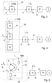
- FIG. 3 shows a simplified block diagram of the device 100 according to the invention.
- an inverter 20 which supplies an electrical load 9 with an alternating voltage
- a driver module 33 is used here, which controls a semiconductor switch of the inverter 20 as a function of a pulse signal PWM.
- a switching arrangement 30 connected to the driver module 33 is provided, which has a switching connection K for applying a blocking signal S and a first connection I for applying the pulse signal PWM in order to switch the pulse signal PWM present at the first connection I through to the driver module 33 on the output connection E or to block it depending on the blocking signal S.
- an interruption of the energy or supply voltage Vcc of the driver module 33 is not provided.
- blocking means interrupting a signal path to driver module 33. If this signal path is not blocked or interrupted, the PWM pulse signal is switched through to driver module 33 or forwarded to it, and driver module 33 can output a control signal 43 to inverter 20. Only then can an electrical load 9 be supplied with an alternating voltage.
- a switching arrangement 30 is used to directly interrupt the signal path of the PWM pulse signal to driver module 33. In this way, an already mentioned Safety function implemented.
- the switching arrangement 30 is switched, as required, via the blocking signal S, which is provided, for example, by a higher-level control device not shown in detail.
- Figure 4 shows the block diagram of an advantageous embodiment of the device 100 according to the invention.
- the switching arrangement 30 is formed by a series connection of a switching element 31, an upstream high-impedance series resistor 34, and a downstream low-impedance load resistor 35.
- the switching element 31 has the switching terminal K, the output terminal E of the switching arrangement 30, and the input terminal B.
- the high-impedance series resistor 34 has the first terminal I.
- a second terminal of the high-impedance series resistor 34 is connected to an input terminal B of the switching element 31.
- the output terminal E of the switching element 31 is connected to the low-impedance load resistor 35.
- the driver module 33 has a driver input 61, which is connected to the output terminal E of the switching element 31.
- the driver module 33 further has a control output 62, which is connected to a semiconductor switch of the inverter 20.
- Figure 5 shows a further advantageous embodiment in which the switching element 31 is embodied by a transistor T in a collector circuit and the input terminal B is formed by its base, the switching terminal K by its collector and the output terminal E by its emitter.
- Transistors are cost-effective components, have short switching times, are maintenance-free, space-saving and have a long service life. Nevertheless, the use of a corresponding logic gate instead of the transistor T as the switching element 31 would also be conceivable. Other transistor circuits can also be used if necessary. In the following, however, reference is made to the particularly advantageous embodiment using a transistor T in a collector circuit (also referred to as an emitter follower).
- the current flowing through the input terminal B (here, the base of the transistor T) is known to be lower by the current gain than through the output terminal E (here, the emitter of the transistor T).
- the high-ohmic series resistor 34 connected to the input terminal B causes a negligible voltage drop, resulting in a voltage gain of approximately one.
- the current gain only occurs when a voltage is applied between the switching terminal K (here, the collector of the transistor T) and the output terminal E.
- the switching terminal K is supplied with voltage due to the blocking signal S applied to an input terminal 39, current amplification occurs and the pulse signal PWM, which is applied to the input terminal B or the base of the transistor T, is passed through to the output terminal E almost unchanged.
- the pulse signal PWM is considerably attenuated according to the voltage divider rule, whereby the voltage divider is formed from the high-ohm series resistor 34 and the low-ohm load resistor 35.
- the voltage drop across the low-ohm load resistor 35 is too low to drive the driver module 33.
- Fail-safe resistors also known as field-proven resistors
- the high-ohm series resistor 34 is formed by a series connection of two high-ohm series resistors 34.
- the low-ohm load resistor 35 is formed by a parallel connection of two low-ohm load resistors 35. The resistance ratio is selected such that the required voltage attenuation is guaranteed even in the event of a total failure of one of the high-ohm series resistors and/or low-ohm load resistors 34, 35.
- the driver module 33 could be activated.
- the high-ohm series resistor 34 must never become low-ohm and the load resistor 35 must never become high-ohm.
- High- and low-resistance means that the low-resistance working resistor 35 has a lower electrical resistance than the high-resistance series resistor 34.
- the necessary control signal 43 for controlling a semiconductor switch 3 can only be provided by the driver module 33 if a blocking signal S, in particular in the form of an electrical voltage, is present at the switching terminal K of the transistor T. Therefore, if the blocking signal S is not provided or interrupted, the electrical load 9 is not controlled because the pulse signal PWM is not switched through.
- the blocking signal S is not applied directly to the switching terminal K of the switching element 31 or to the collector of the transistor T.
- the blocking signal S can be passed through a series circuit 101 before the switching element 31.
- ballast circuit 101 or its three associated functional units current source 40, charging device 50 and optical coupling 60, are described with reference to Figure 6 , which shows a circuit diagram of the device 100 according to the invention in a particularly advantageous embodiment.
- ballast circuit 101 which only includes the current source 40.
- the circuit can be divided into several equal parts, for example, three for the three phases of the three-phase network, at node 22.
- the semiconductor components 4, 6, and 8 above the nodes 16, 17, and 18 are known to be high-side semiconductor components due to their position in the circuit, and the semiconductor components 3, 5, and 7 are known to be low-side semiconductor components.
- the device 100 can, of course, also be used in conjunction with inverters having a different structure than the one just mentioned.
- the functional units storage capacitor and current source 40 shown to the right of node 22 and also the switching arrangement 30 can in this case be designed separately and in the same way for each of the three phases or for each switching element 31, as in Figure 6 indicated.
- test gaps periodic, short-term voltage dips, referred to as test gaps, with a duration of, for example, 60 - 400 ⁇ s, can occur in the blocking signal S.
- test gaps with a duration of, for example, 60 - 400 ⁇ s.
- the higher-level control device uses these test gaps to check its own functionality.
- the interruption of the blocking signal S merely serves test purposes and does not correspond to the activation of the safety function, the device 100 must continue to control the semiconductor switch 3 or the electrical load 9 must continue to be supplied with alternating voltage during the test gap.
- a ballast circuit 101 is connected upstream of the switching arrangement 30.
- the ballast circuit 101 includes a storage capacitor 32 with a charging device 50 and a discharging device 41.
- the charging device 50 is connected to the storage capacitor 32.
- the storage capacitor 32 is connected to the discharging device 41 and the switching terminal K of the switching arrangement 30.
- the storage capacitor 32 is continuously charged by the charging device 50, consisting of at least one transfer capacitor 36. This ensures a certain charge level of the storage capacitor 32, so that the aforementioned test gaps can be bridged. In principle, the storage capacitor 32 continues to supply the switching arrangement 30 with energy via the switching terminal K during the test gaps.
- the storage capacitor 32 is preferably dimensioned such that it just makes it possible to bridge a test gap of a specified length and to supply the switching element 31 with current during the test gap.
- the discharge device 41 ensures that the storage capacitor 32 is discharged continuously or within a predictable time via at least one base load resistor 23.
- the discharge device 41 is connected to the switching element 31 and, in combination with the storage capacitor 32, simultaneously represents the current source via which the switching element 31 or the transistor T is supplied with current.
- the discharge device 41 is advantageously a constant current source, which can be operated in a known manner, as in Figure 6 can be seen, can be constructed from a first control transistor 46 and a second control transistor 49 connected thereto.
- the storage capacitor 32 is discharged within a predictable time not only by the current supplied to the switching element 31, but also via the discharge device 41. Power is only supplied to the switching element during this predictable time. This minimizes the time delay and enables a significantly faster triggering of the safety function than without continuous discharge of the storage capacitor 32 by a discharge device. 41.
- a Zener diode 42 is arranged in parallel with the storage capacitor 32. This simply ensures that, in the event of a potentially excessive voltage level, the storage capacitor 32 is not charged higher than the breakdown voltage of the Zener diode 42 allows. This allows the storage capacitor 32 to be maintained at a defined voltage.
- the storage capacitor 32 is continuously charged by the upstream charging device 50 when a blocking signal S is provided, which is described together with the functional block of the optical coupling 60.
- the storage capacitor 32 is supplied without a galvanic connection to the input terminal 39, to which the blocking signal S is applied.
- a conventional input protection device can be provided at the input of the device 100. This protects the downstream components in a known manner against overvoltages, reverse polarity, etc. Such a device is well known in control engineering, which is why this circuit section will not be discussed in detail.
- the galvanic isolation is achieved within the optical coupling 60 by a first optocoupler 37.
- the energy is transferred capacitively via the charging device 50.
- the first optocoupler 37 could establish a continuous coupling. This would result in a constant voltage level at the output 372 of the optocoupler 37.
- the subsequent charging device 50 consists of at least one transfer capacitor 36, which, as is known, can only transfer alternating voltage, the storage capacitor 32 would not be charged.
- the blocking signal S is formed by a DC voltage.
- the optical coupling 60 in the ballast circuit 101 is dynamized to convert the blocking signal S into an AC voltage.
- the AC voltage is then transmitted to the charging device 50, which is connected to the optical coupling 60.
- the device 100 is dynamized within its ballast circuit 101 or the optical coupling 60. This is achieved by a feedback loop 81 integrated in the optical coupling 60, consisting of at least one hysteresis comparator 45, a delay element 56, and a second optocoupler 38.
- the starting point for the dynamization is that the blocking signal S is applied in the form of a DC voltage to the first optocoupler 37 and activates it.
- the secondary side 372 of the first optocoupler 37 is connected to the hysteresis comparator 45 via a delay element 56.
- the delay element 56 contains a capacitor, hereinafter referred to as the dynamizing capacitor.
- the first optocoupler 37 is deactivated.
- the dynamizing capacitor is then discharged until the hysteresis comparator 45 reaches its lower switching threshold, as a result of which no more high signals are passed to the second optocoupler 38. This is therefore deactivated again, the blocking signal S is again present at the first optocoupler 37 and supplies it again.
- a driver stage 55 is provided between the optical coupler 60 and the charging device 50, which amplifies the output signal 54 of the optical coupler 60 in a known manner, so that the charging device 50 has sufficient energy available for further transmission.
- the aforementioned transfer capacitor 36 is formed by a series connection of several transfer capacitors 36. Should one of the transfer capacitors 36 be defective and cause a short circuit, in the case of a permanently conductive optocoupler, no energy transfer will occur due to an additional transfer capacitor 36.
- Figure 6 For example, two transfer capacitors 36 are connected in series.
- the inductance 44 of the charging device 50 which is also connected in series with the transfer capacitor 36, is advantageous but not absolutely necessary. It primarily serves to increase the voltage and prevent charging current peaks.
- the bandpass behavior, i.e., the blocking of frequencies outside a desired passband, through the combination of inductance and transfer capacitor is also advantageous.
- the first Zener diode 47 provided in the optical coupling 60 in the area of the first optocoupler 37 ensures that the switch-on threshold is at least as high as required for control inputs in relevant Standards stipulate. Only when the breakdown voltage, usually in the range of five volts, of the first Zener diode 47 is reached can the first optocoupler 37 be activated.
- the additional, appropriately dimensioned second Zener diode 48 in the area of the second optocoupler 38 ensures that the previously described dynamization is not possible in the event of a failure or short circuit of the first Zener diode 47. In the event of a short circuit or an insufficient breakdown voltage of the first Zener diode 47, the first optocoupler 37 could not be blocked by the second optocoupler 38.
- the first optocoupler 37 would be continuously active while a blocking signal S is present at terminal 39, which would correspond to a DC voltage signal. Although this would not be a "dangerous" state, since the driver module 33 should be controlled anyway when the blocking signal S is present, the aforementioned dynamization is missing. As a result, no energy can be transferred via the downstream charging device 50. Such a fault in the optical coupling 60 is thus immediately detectable, since the driver module 33 is no longer controlled, even though the blocking signal S is not interrupted.
- the Figure 6 The third Zener diode 63 shown in the area of the optical coupling 60 serves as a safety feature with respect to an overvoltage of the electrical supply voltage V14.
- the Zener diode 63 becomes conductive, and as a result, the aforementioned hysteresis comparator 45 continuously outputs a high signal.
- the optical coupling 60 does not generate any alternating voltage that could be transmitted via the charging device 50.
- the safety function is requested, for example, by the higher-level control unit (not shown in detail), no voltage is applied to input terminal 39. Subsequently, storage capacitor 32 is no longer charged because optical coupling 60 does not generate any alternating voltage and no energy is transported via charging device 50. If no control signals 43 are output during this time and therefore switching arrangement 30 does not receive any current, discharge device 40 must dissipate the electrical energy stored in storage capacitor 32 by another route. This can be done, for example, via a Zener diode connected in parallel to switching arrangement 30 or, as shown in Fig. 6 shown, by a base load resistor 23. The fact that the storage capacitor 32 is discharged continuously and in every case, as described above, ensures that the discharge takes place in a predictable time.
- the device 100 is advantageously used for the safe pulse blocking of an electrical load controlled by an inverter 20.
- the electrical load 9 is advantageously formed by an AC drive.
- AC drive refers to conventional electric drives such as AC motors, three-phase motors, and the like. Due to the processes described above, the AC drive is no longer supplied with AC voltage if the blocking signal S is not applied to input terminal 39. This results in a pulse block, and the AC drive is switched to a torque-free state. In this way, the device 100 for an AC drive implements the Safe Torque Off function already mentioned above.
Landscapes
- Engineering & Computer Science (AREA)
- Power Engineering (AREA)
- Physics & Mathematics (AREA)
- General Physics & Mathematics (AREA)
- Automation & Control Theory (AREA)
- Inverter Devices (AREA)
Claims (15)
- Dispositif (100) permettant la commande sécurisée d'au moins un module de pilote (33) pour commander un commutateur à semi-conducteur (3) d'un onduleur (20), le module de pilote (33) commandant le commutateur à semi-conducteur en fonction d'un signal d'impulsion (PWM), un agencement de commutation (30) relié au module de pilote (33) étant prévu, caractérisé en ce que l'agencement de commutation (30) présente une borne de commutation (K) pour appliquer un signal de blocage (S) et une première borne (I) pour appliquer le signal d'impulsion (PWM), afin de commuter ou de bloquer le signal d'impulsion (PWM) appliqué à la première borne (I) vers le module de pilotage (33) en fonction du signal de blocage (S) et en ce que l'agencement de commutation (30) est précédé d'un circuit ballast (101), le circuit ballast (101) contient un condensateur de stockage (32) comportant un appareil de charge (50) et un dispositif de décharge (41), l'appareil de charge (50) est connecté au condensateur de stockage (32) et le condensateur de stockage (32) est connecté au dispositif de décharge (41) et à la borne de commutation (K) de l'agencement de commutation (30).
- Dispositif (100) selon la revendication 1, caractérisé en ce que l'agencement de commutation (30) est formé par un circuit en série d'un élément de commutation (31) avec la borne de commutation (K), d'une résistance en série à haute impédance (34) en amont, de préférence formée par le circuit en série de deux résistances en série à haute impédance, avec la première borne (I) et d'une résistance de travail de basse impédance (35) en aval, de préférence formée par un circuit en parallèle de deux résistances de travail de basse impédance, qu'une seconde borne de la résistance en série à haute impédance (34) est connectée à une borne d'entrée (B) de l'élément de commutation (31) et qu'une borne de sortie (E) de l'élément de commutation (31) est connectée à la résistance de travail de basse impédance (35).
- Dispositif (100) selon la revendication 2, caractérisé en ce que l'élément de commutation (31) est réalisé par un transistor (T) dans un circuit à collecteur et que la borne d'entrée (B) est formée sur la base de celui-ci, que la borne de commutation (K) est formée par le collecteur du transistor et que la borne de sortie (E) est formée par l'émetteur du transistor.
- Dispositif (100) selon la revendication 1, caractérisé en ce que l'appareil de charge (50) comprend au moins un condensateur de transmission (36).
- Dispositif (100) selon l'une des revendications 1 ou 4, caractérisé en ce que le circuit ballast (101) contient un couplage optique (60) dynamisé permettant de convertir le signal de blocage (S) en une tension alternative, ledit couplage optique dynamisé étant connecté à l'appareil de charge (50) pour transmettre la tension alternative.
- Dispositif (100) selon la revendication 5, caractérisé en ce que le couplage optique (60) contient une boucle de rétroaction (81) qui est formée au moins par un comparateur d'hystérésis (45), un élément retardateur (56) et un optocoupleur (38).
- Dispositif (100) selon l'une des revendications 1 à 6, caractérisé en ce que le dispositif de décharge (41) est connecté à l'élément de commutation (31) pour alimenter en courant électrique l'élément de commutation (31).
- Procédé permettant la commande sécurisée d'un commutateur à semi-conducteur (30) d'un onduleur (20) qui alimente une charge électrique (9) comportant une tension alternative, le commutateur à semi-conducteur (30) étant commandé par l'intermédiaire d'un module de commande (33) en fonction d'un signal d'impulsion (PWM), caractérisé en ce que le signal d'impulsion (PWM) appliqué au module de commande (33) est commuté ou bloqué au moyen d'un élément de commutation (31) en fonction d'un signal de blocage (S) en ce que l'agencement de commutation (30) est précédé d'un circuit ballast (101), le circuit ballast (101) contient un condensateur de stockage (32) comportant un appareil de charge (50) et un dispositif de décharge (41), l'appareil de charge (50) est connecté au condensateur de stockage (32) et le condensateur de stockage (32) est connecté au dispositif de décharge (41) et à la borne de commutation (K) de l'agencement de commutation (30).
- Procédé selon la revendication 8, caractérisé en ce que l'élément de commutation (31) est alimenté en courant par un dispositif de décharge (41) dans lequel un condensateur de stockage (32) est déchargé en continu par le dispositif de décharge (41) par l'intermédiaire d'au moins une résistance de charge de base (23).
- Procédé selon la revendication 9, caractérisé en ce que le condensateur de stockage (32) est chargé en continu par un appareil de charge (50) comprenant au moins un condensateur de transmission (36).
- Procédé selon la revendication 10, caractérisé en ce que l'appareil de charge (50) est alimenté en tension alternative par un couplage optique (60) dynamisé.
- Procédé selon la revendication 11, caractérisé en ce que le signal de blocage (S) appliqué au couplage optique (60) est dynamisé à l'aide d'un premier optocoupleur (37) et d'une boucle de rétroaction (81), constituée d'au moins un comparateur d'hystérésis (45), un élément retardateur (56) et un second optocoupleur (38) dans le couplage optique (60).
- Utilisation du dispositif (100) selon les revendications 1 à 7 permettant le blocage sécurisé d'impulsions d'une charge électrique (9) commandée par un onduleur (20).
- Utilisation du dispositif (100) selon la revendication 13, caractérisée en ce que la charge électrique (9) est formée par un entraînement à courant alternatif.
- Dispositif (100) permettant la commande sécurisée d'au moins un module de pilote (33) pour commander un commutateur à semi-conducteur (3) d'un onduleur (20), le module de pilote (33) commandant le commutateur à semi-conducteur en fonction d'un signal d'impulsion (PWM), un agencement de commutation (30) relié au module de pilote (33) étant prévu, caractérisé en ce que l'agencement de commutation (30) présente une borne de commutation (K) pour appliquer un signal de blocage (S) et une première borne (I) pour appliquer le signal d'impulsion (PWM), afin de commuter ou de bloquer le signal d'impulsion (PWM) appliqué à la première borne (I) vers le module de pilotage (33) en fonction du signal de blocage (S) et en ce que l'agencement de commutation (30) est formé par un circuit en série d'un élément de commutation (31) avec la borne de commutation (K), d'une résistance en série à haute impédance (34) en amont, avec la première borne (I) et d'une résistance de travail de basse impédance (35) en aval, qu'une seconde borne de la résistance en série à haute impédance (34) est connectée à une borne d'entrée (B) de l'élément de commutation (31) et qu'une borne de sortie (E) de l'élément de commutation (31) est connectée à la résistance de travail de basse impédance (35).
Applications Claiming Priority (1)
| Application Number | Priority Date | Filing Date | Title |
|---|---|---|---|
| ATA50846/2014A AT516568B1 (de) | 2014-11-21 | 2014-11-21 | Vorrichtung und ein Verfahren zur sicheren Ansteuerung eines Halbleiterschalters eines Wechselrichters |
Publications (3)
| Publication Number | Publication Date |
|---|---|
| EP3048721A1 EP3048721A1 (fr) | 2016-07-27 |
| EP3048721B1 EP3048721B1 (fr) | 2021-06-30 |
| EP3048721B2 true EP3048721B2 (fr) | 2025-06-04 |
Family
ID=54539844
Family Applications (1)
| Application Number | Title | Priority Date | Filing Date |
|---|---|---|---|
| EP15192929.6A Active EP3048721B2 (fr) | 2014-11-21 | 2015-11-04 | Dispositif et procede de commande fiable d'un circuit semi-conducteur d'un onduleur |
Country Status (5)
| Country | Link |
|---|---|
| US (2) | US9906163B2 (fr) |
| EP (1) | EP3048721B2 (fr) |
| AT (1) | AT516568B1 (fr) |
| CA (1) | CA2911627A1 (fr) |
| DK (1) | DK3048721T3 (fr) |
Families Citing this family (8)
| Publication number | Priority date | Publication date | Assignee | Title |
|---|---|---|---|---|
| IN2014DN09630A (fr) | 2012-05-15 | 2015-07-31 | Otis Elevator Co | |
| AT516568B1 (de) * | 2014-11-21 | 2017-03-15 | Bernecker + Rainer Industrie-Elektronik Ges M B H | Vorrichtung und ein Verfahren zur sicheren Ansteuerung eines Halbleiterschalters eines Wechselrichters |
| US10998832B2 (en) * | 2016-10-05 | 2021-05-04 | Mitsubishi Electric Corporation | Signal transmission circuit and power conversion device |
| KR101872797B1 (ko) * | 2017-05-18 | 2018-06-29 | 두산중공업 주식회사 | 디지털 신호 출력 장치 |
| EP3460593B1 (fr) | 2017-09-22 | 2021-06-30 | B&R Industrial Automation GmbH | Dispositif de commutation sécurisé |
| DE102018115295A1 (de) * | 2018-06-26 | 2020-01-02 | Valeo Siemens Eautomotive Germany Gmbh | Steuerungseinrichtung sowie Verfahren zum Entladen eines Zwischenkreiskondensators, Stromrichter und Fahrzeug |
| FR3103914A1 (fr) * | 2019-11-28 | 2021-06-04 | Schneider Electric Industries Sas | Dispositif de commande sécurisée, contacteur comportant un tel dispositif et procédé de traitement sécurisé d’un signal de commande |
| CN115367575B (zh) * | 2022-08-03 | 2024-07-02 | 上海新时达电气股份有限公司 | 电梯安全控制装置及其控制方法 |
Citations (3)
| Publication number | Priority date | Publication date | Assignee | Title |
|---|---|---|---|---|
| EP1542330A2 (fr) † | 2003-12-08 | 2005-06-15 | Rockwell Automation Technologies, Inc. | Dispositif et procédé servant a désactiver des dispositifs à puissance élevée |
| JP2010104187A (ja) † | 2008-10-27 | 2010-05-06 | Yaskawa Electric Corp | 安全停止回路を備えたモータ制御装置 |
| EP3065290A1 (fr) † | 2013-10-30 | 2016-09-07 | Kabushiki Kaisha Yaskawa Denki | Dispositif de commande de moteur |
Family Cites Families (18)
| Publication number | Priority date | Publication date | Assignee | Title |
|---|---|---|---|---|
| US5485341A (en) * | 1992-09-21 | 1996-01-16 | Kabushiki Kaisha Toshiba | Power transistor overcurrent protection circuit |
| DE69737379T2 (de) * | 1996-04-23 | 2007-10-31 | Denso Corp., Kariya | Spannungsregelungssystem für ein Fahrzeug mit Lichtmaschine |
| US6127788A (en) * | 1997-05-15 | 2000-10-03 | Denso Corporation | High voltage discharge lamp device |
| US6072302A (en) * | 1998-08-26 | 2000-06-06 | Northrop Grumman Corporation | Integrated control system and method for controlling mode, synchronization, power factor, and utility outage ride-through for micropower generation systems |
| JP3983622B2 (ja) | 2002-08-08 | 2007-09-26 | 三菱電機株式会社 | パワーデバイス駆動回路 |
| US7253577B2 (en) | 2005-05-20 | 2007-08-07 | Rockwell Automation Technologies, Inc. | Independent safety processor for disabling the operation of high power devices |
| FR2911736B1 (fr) * | 2007-01-23 | 2009-03-20 | Schneider Toshiba Inverter | Dispositif de commande d'un interrupteur de puissance et variateur comprenant un tel dipositif. |
| DE102008027113A1 (de) * | 2008-06-06 | 2009-12-10 | Siemens Aktiengesellschaft | Verfahren und Vorrichtung zur Steuerung eines Motors |
| JP4817084B2 (ja) * | 2010-03-30 | 2011-11-16 | 株式会社安川電機 | モータ駆動システム及びモータ制御装置 |
| EP2405568B1 (fr) | 2010-07-05 | 2013-08-14 | Gefran S.p.A. | Appareil électronique pour contrôler le mouvement de moteurs électriques à courant alternatif (CA) arrêtant ces moteurs de manière sécurisée |
| DE102011003922A1 (de) | 2011-02-10 | 2012-08-16 | Lenze Automation Gmbh | Steuergerät mit Safe-Torque-Off-Funktion für einen Elektromotor |
| JP5652240B2 (ja) | 2011-02-18 | 2015-01-14 | 株式会社デンソー | 電動コンプレッサ |
| JP5379880B2 (ja) | 2012-04-18 | 2013-12-25 | 三菱電機株式会社 | 電動機駆動制御装置 |
| EP2725435B1 (fr) | 2012-10-24 | 2014-12-10 | Baumüller Nürnberg GmbH | Commande d'une fonction de sécurité d'une machine électrique |
| JP6075024B2 (ja) | 2012-11-19 | 2017-02-08 | 富士電機株式会社 | マルチレベルインバータ |
| JP6329944B2 (ja) | 2013-05-10 | 2018-05-23 | 株式会社日立製作所 | 絶縁ゲート型半導体素子の制御装置およびそれを用いた電力変換装置 |
| AT516568B1 (de) * | 2014-11-21 | 2017-03-15 | Bernecker + Rainer Industrie-Elektronik Ges M B H | Vorrichtung und ein Verfahren zur sicheren Ansteuerung eines Halbleiterschalters eines Wechselrichters |
| GB2532974A (en) | 2014-12-03 | 2016-06-08 | Control Techniques Ltd | Fail-safe interface |
-
2014
- 2014-11-21 AT ATA50846/2014A patent/AT516568B1/de not_active IP Right Cessation
-
2015
- 2015-11-04 DK DK15192929.6T patent/DK3048721T3/da active
- 2015-11-04 EP EP15192929.6A patent/EP3048721B2/fr active Active
- 2015-11-09 CA CA2911627A patent/CA2911627A1/fr not_active Abandoned
- 2015-11-20 US US14/947,000 patent/US9906163B2/en active Active
-
2017
- 2017-11-14 US US15/812,511 patent/US10110144B2/en active Active
Patent Citations (3)
| Publication number | Priority date | Publication date | Assignee | Title |
|---|---|---|---|---|
| EP1542330A2 (fr) † | 2003-12-08 | 2005-06-15 | Rockwell Automation Technologies, Inc. | Dispositif et procédé servant a désactiver des dispositifs à puissance élevée |
| JP2010104187A (ja) † | 2008-10-27 | 2010-05-06 | Yaskawa Electric Corp | 安全停止回路を備えたモータ制御装置 |
| EP3065290A1 (fr) † | 2013-10-30 | 2016-09-07 | Kabushiki Kaisha Yaskawa Denki | Dispositif de commande de moteur |
Also Published As
| Publication number | Publication date |
|---|---|
| AT516568B1 (de) | 2017-03-15 |
| US10110144B2 (en) | 2018-10-23 |
| EP3048721B1 (fr) | 2021-06-30 |
| US20160149514A1 (en) | 2016-05-26 |
| DK3048721T3 (da) | 2021-07-26 |
| EP3048721A1 (fr) | 2016-07-27 |
| US20180069489A1 (en) | 2018-03-08 |
| AT516568A1 (de) | 2016-06-15 |
| CA2911627A1 (fr) | 2016-05-21 |
| US9906163B2 (en) | 2018-02-27 |
Similar Documents
| Publication | Publication Date | Title |
|---|---|---|
| EP3048721B1 (fr) | Dispositif et procede de commande fiable d'un circuit semi-conducteur d'un onduleur | |
| DE3882902T2 (de) | Wechselstrommotorregelungssystem mit notsteuerung. | |
| EP3460593B1 (fr) | Dispositif de commutation sécurisé | |
| EP3022836A1 (fr) | Protection contre les surtensions pour redresseurs actifs en cas de délestage brusque | |
| DE102021122687A1 (de) | Anordnung und Verfahren zur Entladung eines Zwischenkreiskondensators | |
| EP4179621A1 (fr) | Technologie pour permettre l'actionnement d'un étage de puissance | |
| DE102015217533A1 (de) | Entladen von Stützkondensator durch Konstantstrom | |
| EP3138192B1 (fr) | Dispositif permettant de faire fonctionner un redresseur, en particulier un pont redresseur semi-commandé, et procédé permettant de faire fonctionner un redresseur | |
| EP3491738B1 (fr) | Procédé et dispositif d'excitation d'un commutateur statique | |
| DE102006030448B4 (de) | Sichere Ausgangsschaltung mit einem einkanaligen Peripherieanschluss für den Ausgang eines Bus-Teilnehmers | |
| DE102021206853B3 (de) | Treiberschaltung mit zwei kaskadierten Halbbrückentreibern zur Ansteuerung von drei Transistoren | |
| EP2893603B1 (fr) | Procédé de commande d'un redresseur en pont actif lors d'un délestage, système redresseur et produit logiciel informatique | |
| EP3017543B1 (fr) | Montage électronique pour la protection d'au moins un composant d'un circuit de courant à deux fils | |
| EP2503669B1 (fr) | Système d'automatisation de sécurite avec comportement de commutation contrôlé et avec dispositif d'accélération de commutation | |
| DE102016010777B4 (de) | Antrieb mit Sicherheitsschaltvorrichtung, System und Verfahren | |
| DE102004013108B4 (de) | Verfahren zum Betreiben einer Versorgungseinheit für eine Treiberschaltung sowie Versorgungseinheit für eine Treiberschaltung | |
| WO2015082190A1 (fr) | Ensemble circuit | |
| WO2023020996A1 (fr) | Dispositif de décharge | |
| EP2669233A1 (fr) | Circuit de commande de freinage pour un frein actionné de manière électromagnétique et module d'entraînement | |
| EP3061186B1 (fr) | Demi-pont pour redresseur actif | |
| DE102014008906A1 (de) | Elektronisches Relais | |
| WO2007085372A1 (fr) | Dispositif de commutation de sécurité et procédé d'arrêt sécurisé d'un récepteur électrique | |
| EP3956960B1 (fr) | Système comprenant au moins deux consommateurs connectés à une ligne d'alimentation commune et pouvant être désactivés sélectivement et utilisation d'au moins un élément de commutation d'interruption comprenant un allumeur activable de l'extérieur pour la séparation sûre d'un consommateur d'un réseau électrique d'alimentation | |
| EP4510452A1 (fr) | Protection contre les surtensions pour un élément de commutation électronique | |
| WO2025083220A1 (fr) | Appareil et procédé de décharge passive d'un dispositif de stockage d'énergie |
Legal Events
| Date | Code | Title | Description |
|---|---|---|---|
| PUAI | Public reference made under article 153(3) epc to a published international application that has entered the european phase |
Free format text: ORIGINAL CODE: 0009012 |
|
| AK | Designated contracting states |
Kind code of ref document: A1 Designated state(s): AL AT BE BG CH CY CZ DE DK EE ES FI FR GB GR HR HU IE IS IT LI LT LU LV MC MK MT NL NO PL PT RO RS SE SI SK SM TR |
|
| AX | Request for extension of the european patent |
Extension state: BA ME |
|
| STAA | Information on the status of an ep patent application or granted ep patent |
Free format text: STATUS: REQUEST FOR EXAMINATION WAS MADE |
|
| 17P | Request for examination filed |
Effective date: 20170125 |
|
| RBV | Designated contracting states (corrected) |
Designated state(s): AL AT BE BG CH CY CZ DE DK EE ES FI FR GB GR HR HU IE IS IT LI LT LU LV MC MK MT NL NO PL PT RO RS SE SI SK SM TR |
|
| RAP1 | Party data changed (applicant data changed or rights of an application transferred) |
Owner name: B&R INDUSTRIAL AUTOMATION GMBH |
|
| STAA | Information on the status of an ep patent application or granted ep patent |
Free format text: STATUS: EXAMINATION IS IN PROGRESS |
|
| 17Q | First examination report despatched |
Effective date: 20180207 |
|
| TPAC | Observations filed by third parties |
Free format text: ORIGINAL CODE: EPIDOSNTIPA |
|
| GRAP | Despatch of communication of intention to grant a patent |
Free format text: ORIGINAL CODE: EPIDOSNIGR1 |
|
| STAA | Information on the status of an ep patent application or granted ep patent |
Free format text: STATUS: GRANT OF PATENT IS INTENDED |
|
| INTG | Intention to grant announced |
Effective date: 20210223 |
|
| GRAS | Grant fee paid |
Free format text: ORIGINAL CODE: EPIDOSNIGR3 |
|
| GRAA | (expected) grant |
Free format text: ORIGINAL CODE: 0009210 |
|
| STAA | Information on the status of an ep patent application or granted ep patent |
Free format text: STATUS: THE PATENT HAS BEEN GRANTED |
|
| AK | Designated contracting states |
Kind code of ref document: B1 Designated state(s): AL AT BE BG CH CY CZ DE DK EE ES FI FR GB GR HR HU IE IS IT LI LT LU LV MC MK MT NL NO PL PT RO RS SE SI SK SM TR |
|
| REG | Reference to a national code |
Ref country code: CH Ref legal event code: EP |
|
| REG | Reference to a national code |
Ref country code: AT Ref legal event code: REF Ref document number: 1407303 Country of ref document: AT Kind code of ref document: T Effective date: 20210715 |
|
| REG | Reference to a national code |
Ref country code: DE Ref legal event code: R096 Ref document number: 502015014870 Country of ref document: DE |
|
| REG | Reference to a national code |
Ref country code: DK Ref legal event code: T3 Effective date: 20210720 |
|
| REG | Reference to a national code |
Ref country code: IE Ref legal event code: FG4D Free format text: LANGUAGE OF EP DOCUMENT: GERMAN |
|
| REG | Reference to a national code |
Ref country code: SE Ref legal event code: TRGR |
|
| REG | Reference to a national code |
Ref country code: LT Ref legal event code: MG9D |
|
| PG25 | Lapsed in a contracting state [announced via postgrant information from national office to epo] |
Ref country code: FI Free format text: LAPSE BECAUSE OF FAILURE TO SUBMIT A TRANSLATION OF THE DESCRIPTION OR TO PAY THE FEE WITHIN THE PRESCRIBED TIME-LIMIT Effective date: 20210630 Ref country code: BG Free format text: LAPSE BECAUSE OF FAILURE TO SUBMIT A TRANSLATION OF THE DESCRIPTION OR TO PAY THE FEE WITHIN THE PRESCRIBED TIME-LIMIT Effective date: 20210930 Ref country code: HR Free format text: LAPSE BECAUSE OF FAILURE TO SUBMIT A TRANSLATION OF THE DESCRIPTION OR TO PAY THE FEE WITHIN THE PRESCRIBED TIME-LIMIT Effective date: 20210630 |
|
| REG | Reference to a national code |
Ref country code: NL Ref legal event code: MP Effective date: 20210630 |
|
| PG25 | Lapsed in a contracting state [announced via postgrant information from national office to epo] |
Ref country code: LV Free format text: LAPSE BECAUSE OF FAILURE TO SUBMIT A TRANSLATION OF THE DESCRIPTION OR TO PAY THE FEE WITHIN THE PRESCRIBED TIME-LIMIT Effective date: 20210630 Ref country code: GR Free format text: LAPSE BECAUSE OF FAILURE TO SUBMIT A TRANSLATION OF THE DESCRIPTION OR TO PAY THE FEE WITHIN THE PRESCRIBED TIME-LIMIT Effective date: 20211001 Ref country code: NO Free format text: LAPSE BECAUSE OF FAILURE TO SUBMIT A TRANSLATION OF THE DESCRIPTION OR TO PAY THE FEE WITHIN THE PRESCRIBED TIME-LIMIT Effective date: 20210930 Ref country code: RS Free format text: LAPSE BECAUSE OF FAILURE TO SUBMIT A TRANSLATION OF THE DESCRIPTION OR TO PAY THE FEE WITHIN THE PRESCRIBED TIME-LIMIT Effective date: 20210630 |
|
| PG25 | Lapsed in a contracting state [announced via postgrant information from national office to epo] |
Ref country code: EE Free format text: LAPSE BECAUSE OF FAILURE TO SUBMIT A TRANSLATION OF THE DESCRIPTION OR TO PAY THE FEE WITHIN THE PRESCRIBED TIME-LIMIT Effective date: 20210630 Ref country code: CZ Free format text: LAPSE BECAUSE OF FAILURE TO SUBMIT A TRANSLATION OF THE DESCRIPTION OR TO PAY THE FEE WITHIN THE PRESCRIBED TIME-LIMIT Effective date: 20210630 Ref country code: SM Free format text: LAPSE BECAUSE OF FAILURE TO SUBMIT A TRANSLATION OF THE DESCRIPTION OR TO PAY THE FEE WITHIN THE PRESCRIBED TIME-LIMIT Effective date: 20210630 Ref country code: SK Free format text: LAPSE BECAUSE OF FAILURE TO SUBMIT A TRANSLATION OF THE DESCRIPTION OR TO PAY THE FEE WITHIN THE PRESCRIBED TIME-LIMIT Effective date: 20210630 Ref country code: RO Free format text: LAPSE BECAUSE OF FAILURE TO SUBMIT A TRANSLATION OF THE DESCRIPTION OR TO PAY THE FEE WITHIN THE PRESCRIBED TIME-LIMIT Effective date: 20210630 Ref country code: NL Free format text: LAPSE BECAUSE OF FAILURE TO SUBMIT A TRANSLATION OF THE DESCRIPTION OR TO PAY THE FEE WITHIN THE PRESCRIBED TIME-LIMIT Effective date: 20210630 Ref country code: PT Free format text: LAPSE BECAUSE OF FAILURE TO SUBMIT A TRANSLATION OF THE DESCRIPTION OR TO PAY THE FEE WITHIN THE PRESCRIBED TIME-LIMIT Effective date: 20211102 Ref country code: ES Free format text: LAPSE BECAUSE OF FAILURE TO SUBMIT A TRANSLATION OF THE DESCRIPTION OR TO PAY THE FEE WITHIN THE PRESCRIBED TIME-LIMIT Effective date: 20210630 |
|
| PGFP | Annual fee paid to national office [announced via postgrant information from national office to epo] |
Ref country code: DK Payment date: 20211007 Year of fee payment: 7 Ref country code: GB Payment date: 20211004 Year of fee payment: 7 Ref country code: SE Payment date: 20211018 Year of fee payment: 7 Ref country code: AT Payment date: 20211018 Year of fee payment: 7 |
|
| PG25 | Lapsed in a contracting state [announced via postgrant information from national office to epo] |
Ref country code: PL Free format text: LAPSE BECAUSE OF FAILURE TO SUBMIT A TRANSLATION OF THE DESCRIPTION OR TO PAY THE FEE WITHIN THE PRESCRIBED TIME-LIMIT Effective date: 20210630 |
|
| PGFP | Annual fee paid to national office [announced via postgrant information from national office to epo] |
Ref country code: CH Payment date: 20211025 Year of fee payment: 7 |
|
| REG | Reference to a national code |
Ref country code: DE Ref legal event code: R026 Ref document number: 502015014870 Country of ref document: DE |
|
| PLBI | Opposition filed |
Free format text: ORIGINAL CODE: 0009260 |
|
| PLBI | Opposition filed |
Free format text: ORIGINAL CODE: 0009260 |
|
| PLAX | Notice of opposition and request to file observation + time limit sent |
Free format text: ORIGINAL CODE: EPIDOSNOBS2 |
|
| 26 | Opposition filed |
Opponent name: SEW-EURODRIVE GMBH & CO. KG Effective date: 20220311 |
|
| 26 | Opposition filed |
Opponent name: LENZE SE Effective date: 20220330 |
|
| PG25 | Lapsed in a contracting state [announced via postgrant information from national office to epo] |
Ref country code: AL Free format text: LAPSE BECAUSE OF FAILURE TO SUBMIT A TRANSLATION OF THE DESCRIPTION OR TO PAY THE FEE WITHIN THE PRESCRIBED TIME-LIMIT Effective date: 20210630 |
|
| PG25 | Lapsed in a contracting state [announced via postgrant information from national office to epo] |
Ref country code: MC Free format text: LAPSE BECAUSE OF FAILURE TO SUBMIT A TRANSLATION OF THE DESCRIPTION OR TO PAY THE FEE WITHIN THE PRESCRIBED TIME-LIMIT Effective date: 20210630 |
|
| PG25 | Lapsed in a contracting state [announced via postgrant information from national office to epo] |
Ref country code: LU Free format text: LAPSE BECAUSE OF NON-PAYMENT OF DUE FEES Effective date: 20211104 Ref country code: BE Free format text: LAPSE BECAUSE OF NON-PAYMENT OF DUE FEES Effective date: 20211130 |
|
| REG | Reference to a national code |
Ref country code: BE Ref legal event code: MM Effective date: 20211130 |
|
| PLBB | Reply of patent proprietor to notice(s) of opposition received |
Free format text: ORIGINAL CODE: EPIDOSNOBS3 |
|
| PG25 | Lapsed in a contracting state [announced via postgrant information from national office to epo] |
Ref country code: IE Free format text: LAPSE BECAUSE OF NON-PAYMENT OF DUE FEES Effective date: 20211104 |
|
| PG25 | Lapsed in a contracting state [announced via postgrant information from national office to epo] |
Ref country code: LT Free format text: LAPSE BECAUSE OF FAILURE TO SUBMIT A TRANSLATION OF THE DESCRIPTION OR TO PAY THE FEE WITHIN THE PRESCRIBED TIME-LIMIT Effective date: 20210630 |
|
| PG25 | Lapsed in a contracting state [announced via postgrant information from national office to epo] |
Ref country code: HU Free format text: LAPSE BECAUSE OF FAILURE TO SUBMIT A TRANSLATION OF THE DESCRIPTION OR TO PAY THE FEE WITHIN THE PRESCRIBED TIME-LIMIT; INVALID AB INITIO Effective date: 20151104 |
|
| REG | Reference to a national code |
Ref country code: DK Ref legal event code: EBP Effective date: 20221130 |
|
| PG25 | Lapsed in a contracting state [announced via postgrant information from national office to epo] |
Ref country code: CY Free format text: LAPSE BECAUSE OF FAILURE TO SUBMIT A TRANSLATION OF THE DESCRIPTION OR TO PAY THE FEE WITHIN THE PRESCRIBED TIME-LIMIT Effective date: 20210630 |
|
| REG | Reference to a national code |
Ref country code: CH Ref legal event code: PL |
|
| REG | Reference to a national code |
Ref country code: SE Ref legal event code: EUG |
|
| REG | Reference to a national code |
Ref country code: AT Ref legal event code: MM01 Ref document number: 1407303 Country of ref document: AT Kind code of ref document: T Effective date: 20221104 |
|
| GBPC | Gb: european patent ceased through non-payment of renewal fee |
Effective date: 20221104 |
|
| P01 | Opt-out of the competence of the unified patent court (upc) registered |
Effective date: 20230615 |
|
| PG25 | Lapsed in a contracting state [announced via postgrant information from national office to epo] |
Ref country code: LI Free format text: LAPSE BECAUSE OF NON-PAYMENT OF DUE FEES Effective date: 20221130 Ref country code: CH Free format text: LAPSE BECAUSE OF NON-PAYMENT OF DUE FEES Effective date: 20221130 Ref country code: AT Free format text: LAPSE BECAUSE OF NON-PAYMENT OF DUE FEES Effective date: 20221104 |
|
| PG25 | Lapsed in a contracting state [announced via postgrant information from national office to epo] |
Ref country code: SE Free format text: LAPSE BECAUSE OF NON-PAYMENT OF DUE FEES Effective date: 20221105 |
|
| PG25 | Lapsed in a contracting state [announced via postgrant information from national office to epo] |
Ref country code: GB Free format text: LAPSE BECAUSE OF NON-PAYMENT OF DUE FEES Effective date: 20221104 Ref country code: DK Free format text: LAPSE BECAUSE OF NON-PAYMENT OF DUE FEES Effective date: 20221130 |
|
| PG25 | Lapsed in a contracting state [announced via postgrant information from national office to epo] |
Ref country code: MK Free format text: LAPSE BECAUSE OF FAILURE TO SUBMIT A TRANSLATION OF THE DESCRIPTION OR TO PAY THE FEE WITHIN THE PRESCRIBED TIME-LIMIT Effective date: 20210630 |
|
| PG25 | Lapsed in a contracting state [announced via postgrant information from national office to epo] |
Ref country code: TR Free format text: LAPSE BECAUSE OF FAILURE TO SUBMIT A TRANSLATION OF THE DESCRIPTION OR TO PAY THE FEE WITHIN THE PRESCRIBED TIME-LIMIT Effective date: 20210630 |
|
| PG25 | Lapsed in a contracting state [announced via postgrant information from national office to epo] |
Ref country code: MT Free format text: LAPSE BECAUSE OF FAILURE TO SUBMIT A TRANSLATION OF THE DESCRIPTION OR TO PAY THE FEE WITHIN THE PRESCRIBED TIME-LIMIT Effective date: 20210630 |
|
| APBP | Date of receipt of notice of appeal recorded |
Free format text: ORIGINAL CODE: EPIDOSNNOA2O |
|
| APAH | Appeal reference modified |
Free format text: ORIGINAL CODE: EPIDOSCREFNO |
|
| APAW | Appeal reference deleted |
Free format text: ORIGINAL CODE: EPIDOSDREFNO |
|
| APBU | Appeal procedure closed |
Free format text: ORIGINAL CODE: EPIDOSNNOA9O |
|
| PUAH | Patent maintained in amended form |
Free format text: ORIGINAL CODE: 0009272 |
|
| STAA | Information on the status of an ep patent application or granted ep patent |
Free format text: STATUS: PATENT MAINTAINED AS AMENDED |
|
| REG | Reference to a national code |
Ref country code: DE Ref legal event code: R081 Ref document number: 502015014870 Country of ref document: DE Owner name: ABB SCHWEIZ AG, CH Free format text: FORMER OWNER: B&R INDUSTRIAL AUTOMATION GMBH, EGGELSBERG, AT |
|
| 27A | Patent maintained in amended form |
Effective date: 20250604 |
|
| AK | Designated contracting states |
Kind code of ref document: B2 Designated state(s): AL AT BE BG CH CY CZ DE DK EE ES FI FR GB GR HR HU IE IS IT LI LT LU LV MC MK MT NL NO PL PT RO RS SE SI SK SM TR |
|
| REG | Reference to a national code |
Ref country code: DE Ref legal event code: R102 Ref document number: 502015014870 Country of ref document: DE |
|
| PGFP | Annual fee paid to national office [announced via postgrant information from national office to epo] |
Ref country code: DE Payment date: 20251119 Year of fee payment: 11 |
|
| PGFP | Annual fee paid to national office [announced via postgrant information from national office to epo] |
Ref country code: IT Payment date: 20251125 Year of fee payment: 11 |
|
| PGFP | Annual fee paid to national office [announced via postgrant information from national office to epo] |
Ref country code: FR Payment date: 20251125 Year of fee payment: 11 |