EP3049863B1 - Panneau afficheur avec images pré-formées - Google Patents
Panneau afficheur avec images pré-formées Download PDFInfo
- Publication number
- EP3049863B1 EP3049863B1 EP14846369.8A EP14846369A EP3049863B1 EP 3049863 B1 EP3049863 B1 EP 3049863B1 EP 14846369 A EP14846369 A EP 14846369A EP 3049863 B1 EP3049863 B1 EP 3049863B1
- Authority
- EP
- European Patent Office
- Prior art keywords
- microcells
- area
- display panel
- panel
- solvent
- Prior art date
- Legal status (The legal status is an assumption and is not a legal conclusion. Google has not performed a legal analysis and makes no representation as to the accuracy of the status listed.)
- Active
Links
Images




Classifications
-
- G—PHYSICS
- G02—OPTICS
- G02F—OPTICAL DEVICES OR ARRANGEMENTS FOR THE CONTROL OF LIGHT BY MODIFICATION OF THE OPTICAL PROPERTIES OF THE MEDIA OF THE ELEMENTS INVOLVED THEREIN; NON-LINEAR OPTICS; FREQUENCY-CHANGING OF LIGHT; OPTICAL LOGIC ELEMENTS; OPTICAL ANALOGUE/DIGITAL CONVERTERS
- G02F1/00—Devices or arrangements for the control of the intensity, colour, phase, polarisation or direction of light arriving from an independent light source, e.g. switching, gating or modulating; Non-linear optics
- G02F1/01—Devices or arrangements for the control of the intensity, colour, phase, polarisation or direction of light arriving from an independent light source, e.g. switching, gating or modulating; Non-linear optics for the control of the intensity, phase, polarisation or colour
- G02F1/165—Devices or arrangements for the control of the intensity, colour, phase, polarisation or direction of light arriving from an independent light source, e.g. switching, gating or modulating; Non-linear optics for the control of the intensity, phase, polarisation or colour based on translational movement of particles in a fluid under the influence of an applied field
- G02F1/166—Devices or arrangements for the control of the intensity, colour, phase, polarisation or direction of light arriving from an independent light source, e.g. switching, gating or modulating; Non-linear optics for the control of the intensity, phase, polarisation or colour based on translational movement of particles in a fluid under the influence of an applied field characterised by the electro-optical or magneto-optical effect
- G02F1/167—Devices or arrangements for the control of the intensity, colour, phase, polarisation or direction of light arriving from an independent light source, e.g. switching, gating or modulating; Non-linear optics for the control of the intensity, phase, polarisation or colour based on translational movement of particles in a fluid under the influence of an applied field characterised by the electro-optical or magneto-optical effect by electrophoresis
-
- G—PHYSICS
- G02—OPTICS
- G02B—OPTICAL ELEMENTS, SYSTEMS OR APPARATUS
- G02B26/00—Optical devices or arrangements for the control of light using movable or deformable optical elements
- G02B26/02—Optical devices or arrangements for the control of light using movable or deformable optical elements for controlling the intensity of light
- G02B26/026—Optical devices or arrangements for the control of light using movable or deformable optical elements for controlling the intensity of light based on the rotation of particles under the influence of an external field, e.g. gyricons, twisting ball displays
-
- G—PHYSICS
- G02—OPTICS
- G02F—OPTICAL DEVICES OR ARRANGEMENTS FOR THE CONTROL OF LIGHT BY MODIFICATION OF THE OPTICAL PROPERTIES OF THE MEDIA OF THE ELEMENTS INVOLVED THEREIN; NON-LINEAR OPTICS; FREQUENCY-CHANGING OF LIGHT; OPTICAL LOGIC ELEMENTS; OPTICAL ANALOGUE/DIGITAL CONVERTERS
- G02F1/00—Devices or arrangements for the control of the intensity, colour, phase, polarisation or direction of light arriving from an independent light source, e.g. switching, gating or modulating; Non-linear optics
- G02F1/01—Devices or arrangements for the control of the intensity, colour, phase, polarisation or direction of light arriving from an independent light source, e.g. switching, gating or modulating; Non-linear optics for the control of the intensity, phase, polarisation or colour
- G02F1/13—Devices or arrangements for the control of the intensity, colour, phase, polarisation or direction of light arriving from an independent light source, e.g. switching, gating or modulating; Non-linear optics for the control of the intensity, phase, polarisation or colour based on liquid crystals, e.g. single liquid crystal display cells
- G02F1/133—Constructional arrangements; Operation of liquid crystal cells; Circuit arrangements
- G02F1/1333—Constructional arrangements; Manufacturing methods
- G02F1/1343—Electrodes
- G02F1/134309—Electrodes characterised by their geometrical arrangement
- G02F1/134336—Matrix
-
- G—PHYSICS
- G02—OPTICS
- G02F—OPTICAL DEVICES OR ARRANGEMENTS FOR THE CONTROL OF LIGHT BY MODIFICATION OF THE OPTICAL PROPERTIES OF THE MEDIA OF THE ELEMENTS INVOLVED THEREIN; NON-LINEAR OPTICS; FREQUENCY-CHANGING OF LIGHT; OPTICAL LOGIC ELEMENTS; OPTICAL ANALOGUE/DIGITAL CONVERTERS
- G02F1/00—Devices or arrangements for the control of the intensity, colour, phase, polarisation or direction of light arriving from an independent light source, e.g. switching, gating or modulating; Non-linear optics
- G02F1/01—Devices or arrangements for the control of the intensity, colour, phase, polarisation or direction of light arriving from an independent light source, e.g. switching, gating or modulating; Non-linear optics for the control of the intensity, phase, polarisation or colour
- G02F1/165—Devices or arrangements for the control of the intensity, colour, phase, polarisation or direction of light arriving from an independent light source, e.g. switching, gating or modulating; Non-linear optics for the control of the intensity, phase, polarisation or colour based on translational movement of particles in a fluid under the influence of an applied field
- G02F1/1675—Constructional details
- G02F1/1679—Gaskets; Spacers; Sealing of cells; Filling or closing of cells
-
- G—PHYSICS
- G09—EDUCATION; CRYPTOGRAPHY; DISPLAY; ADVERTISING; SEALS
- G09G—ARRANGEMENTS OR CIRCUITS FOR CONTROL OF INDICATING DEVICES USING STATIC MEANS TO PRESENT VARIABLE INFORMATION
- G09G3/00—Control arrangements or circuits, of interest only in connection with visual indicators other than cathode-ray tubes
- G09G3/20—Control arrangements or circuits, of interest only in connection with visual indicators other than cathode-ray tubes for presentation of an assembly of a number of characters, e.g. a page, by composing the assembly by combination of individual elements arranged in a matrix no fixed position being assigned to or needed to be assigned to the individual characters or partial characters
- G09G3/34—Control arrangements or circuits, of interest only in connection with visual indicators other than cathode-ray tubes for presentation of an assembly of a number of characters, e.g. a page, by composing the assembly by combination of individual elements arranged in a matrix no fixed position being assigned to or needed to be assigned to the individual characters or partial characters by control of light from an independent source
- G09G3/3433—Control arrangements or circuits, of interest only in connection with visual indicators other than cathode-ray tubes for presentation of an assembly of a number of characters, e.g. a page, by composing the assembly by combination of individual elements arranged in a matrix no fixed position being assigned to or needed to be assigned to the individual characters or partial characters by control of light from an independent source using light modulating elements actuated by an electric field and being other than liquid crystal devices and electrochromic devices
- G09G3/344—Control arrangements or circuits, of interest only in connection with visual indicators other than cathode-ray tubes for presentation of an assembly of a number of characters, e.g. a page, by composing the assembly by combination of individual elements arranged in a matrix no fixed position being assigned to or needed to be assigned to the individual characters or partial characters by control of light from an independent source using light modulating elements actuated by an electric field and being other than liquid crystal devices and electrochromic devices based on particles moving in a fluid or in a gas, e.g. electrophoretic devices
-
- G—PHYSICS
- G02—OPTICS
- G02F—OPTICAL DEVICES OR ARRANGEMENTS FOR THE CONTROL OF LIGHT BY MODIFICATION OF THE OPTICAL PROPERTIES OF THE MEDIA OF THE ELEMENTS INVOLVED THEREIN; NON-LINEAR OPTICS; FREQUENCY-CHANGING OF LIGHT; OPTICAL LOGIC ELEMENTS; OPTICAL ANALOGUE/DIGITAL CONVERTERS
- G02F1/00—Devices or arrangements for the control of the intensity, colour, phase, polarisation or direction of light arriving from an independent light source, e.g. switching, gating or modulating; Non-linear optics
- G02F1/01—Devices or arrangements for the control of the intensity, colour, phase, polarisation or direction of light arriving from an independent light source, e.g. switching, gating or modulating; Non-linear optics for the control of the intensity, phase, polarisation or colour
- G02F1/13—Devices or arrangements for the control of the intensity, colour, phase, polarisation or direction of light arriving from an independent light source, e.g. switching, gating or modulating; Non-linear optics for the control of the intensity, phase, polarisation or colour based on liquid crystals, e.g. single liquid crystal display cells
- G02F1/133—Constructional arrangements; Operation of liquid crystal cells; Circuit arrangements
- G02F1/1333—Constructional arrangements; Manufacturing methods
-
- G—PHYSICS
- G02—OPTICS
- G02F—OPTICAL DEVICES OR ARRANGEMENTS FOR THE CONTROL OF LIGHT BY MODIFICATION OF THE OPTICAL PROPERTIES OF THE MEDIA OF THE ELEMENTS INVOLVED THEREIN; NON-LINEAR OPTICS; FREQUENCY-CHANGING OF LIGHT; OPTICAL LOGIC ELEMENTS; OPTICAL ANALOGUE/DIGITAL CONVERTERS
- G02F1/00—Devices or arrangements for the control of the intensity, colour, phase, polarisation or direction of light arriving from an independent light source, e.g. switching, gating or modulating; Non-linear optics
- G02F1/01—Devices or arrangements for the control of the intensity, colour, phase, polarisation or direction of light arriving from an independent light source, e.g. switching, gating or modulating; Non-linear optics for the control of the intensity, phase, polarisation or colour
- G02F1/13—Devices or arrangements for the control of the intensity, colour, phase, polarisation or direction of light arriving from an independent light source, e.g. switching, gating or modulating; Non-linear optics for the control of the intensity, phase, polarisation or colour based on liquid crystals, e.g. single liquid crystal display cells
- G02F1/133—Constructional arrangements; Operation of liquid crystal cells; Circuit arrangements
- G02F1/1333—Constructional arrangements; Manufacturing methods
- G02F1/133371—Cells with varying thickness of the liquid crystal layer
-
- G—PHYSICS
- G02—OPTICS
- G02F—OPTICAL DEVICES OR ARRANGEMENTS FOR THE CONTROL OF LIGHT BY MODIFICATION OF THE OPTICAL PROPERTIES OF THE MEDIA OF THE ELEMENTS INVOLVED THEREIN; NON-LINEAR OPTICS; FREQUENCY-CHANGING OF LIGHT; OPTICAL LOGIC ELEMENTS; OPTICAL ANALOGUE/DIGITAL CONVERTERS
- G02F1/00—Devices or arrangements for the control of the intensity, colour, phase, polarisation or direction of light arriving from an independent light source, e.g. switching, gating or modulating; Non-linear optics
- G02F1/01—Devices or arrangements for the control of the intensity, colour, phase, polarisation or direction of light arriving from an independent light source, e.g. switching, gating or modulating; Non-linear optics for the control of the intensity, phase, polarisation or colour
- G02F1/13—Devices or arrangements for the control of the intensity, colour, phase, polarisation or direction of light arriving from an independent light source, e.g. switching, gating or modulating; Non-linear optics for the control of the intensity, phase, polarisation or colour based on liquid crystals, e.g. single liquid crystal display cells
- G02F1/133—Constructional arrangements; Operation of liquid crystal cells; Circuit arrangements
- G02F1/1333—Constructional arrangements; Manufacturing methods
- G02F1/1347—Arrangement of liquid crystal layers or cells in which the final condition of one light beam is achieved by the addition of the effects of two or more layers or cells
-
- G—PHYSICS
- G02—OPTICS
- G02F—OPTICAL DEVICES OR ARRANGEMENTS FOR THE CONTROL OF LIGHT BY MODIFICATION OF THE OPTICAL PROPERTIES OF THE MEDIA OF THE ELEMENTS INVOLVED THEREIN; NON-LINEAR OPTICS; FREQUENCY-CHANGING OF LIGHT; OPTICAL LOGIC ELEMENTS; OPTICAL ANALOGUE/DIGITAL CONVERTERS
- G02F1/00—Devices or arrangements for the control of the intensity, colour, phase, polarisation or direction of light arriving from an independent light source, e.g. switching, gating or modulating; Non-linear optics
- G02F1/01—Devices or arrangements for the control of the intensity, colour, phase, polarisation or direction of light arriving from an independent light source, e.g. switching, gating or modulating; Non-linear optics for the control of the intensity, phase, polarisation or colour
- G02F1/165—Devices or arrangements for the control of the intensity, colour, phase, polarisation or direction of light arriving from an independent light source, e.g. switching, gating or modulating; Non-linear optics for the control of the intensity, phase, polarisation or colour based on translational movement of particles in a fluid under the influence of an applied field
- G02F1/1675—Constructional details
- G02F1/1679—Gaskets; Spacers; Sealing of cells; Filling or closing of cells
- G02F1/1681—Gaskets; Spacers; Sealing of cells; Filling or closing of cells having two or more microcells partitioned by walls, e.g. of microcup type
Definitions
- the present invention is directed to a display panel with a pre-patterned image.
- a display panel with a pre-patterned image.
- Such a panel has a variety of applications, such as signage display having fixed image patterns, or a watermark feature for protecting against counterfeiting or simply for decoration purposes.
- US 2011/0069001 A1 describes an electronic paper display in which two different types of bichromal spheres are accommodated in recesses of differing depths below a viewing surface, so that the bottom thickness (the distance between the bottom of the recesses and the backplane) varies.
- the published application states that the bichromal spheres may be replaced by electrophoretic capsules; such displays are shown in US2011/133627 .
- US 2005/0152022 describes an encapsulated electrophoretic display in which a shim, disposed between the electrophoretic medium and the rear electrode, or behind the rear electrode, so as to vary the thickness of the electrophoretic layer in the area of the shim, and thus the electro-optic behavior of this portion of the electrophoretic layer.
- the present invention is directed to a display panel comprising microcells filled with an electrophoretic fluid wherein each of the microcells has the form of a cup-like micro-container having a bottom wall.
- the inner surface of the bottom wall is in contact with the electrophoretic fluid.
- the display panel has a first area and a second area, the microcells in the first area having substantially the same bottom wall thickness, and the microcells in the second area have thicker bottom walls than the microcells in the first area.
- the second area of the display panel forms a pre-patterned image, while the first area is a background area, or vice versa.
- the microcells in the second area have a bottom thickness which is 0.001 micron to 9/10 of the depth of the microcells in the first area, more than the bottom thickness of the microcells in the first area.
- the microcells in the second area have a bottom thickness which is 0.001 micron to 1 ⁇ 2 of the depth of the microcells in the first area, more than the bottom thickness of the microcells in the first area.
- the bottom thicknesses of the microcells in the second area vary.
- an electrophoretic fluid filled in the microcells in both the first and second areas comprises one type of charged particles dispersed in a solvent or solvent mixture.
- an electrophoretic fluid filled in the microcells in the first and second areas comprises two types of charged particles dispersed in a solvent or solvent mixture.
- an electrophoretic fluid filled in the microcells in the first and second areas comprises more than two types of charged particles dispersed in a solvent or solvent mixture.
- the display panel is sandwiched between two electrode layers.
- the two electrode layers are non-patterned conductive layers.
- one of the electrode layers is a common electrode layer and the other electrode layer is a thin-film-transistor matrix driving system or segmented backplane driving system.
- the display panel is used in bar codes, anti-counterfeiting labels, direction signage or shelf labels. In another embodiment, the display panel is used in a watermark application.
- Another aspect of the present invention is directed to a method for the preparation of a display panel of the present invention, which comprises:
- the carved-out areas vary in depth.
- the substrate layer is attached to an electrode layer.
- a further aspect of the present invention is directed to a method for the preparation of a display panel of the present invention, which comprises:
- the solvent is methyl ethyl ketone, acetone, or isopropyl alcohol.
- the microcells are filled with different concentrations of chemical compositions. In one embodiment, the concentrations are in the range of 0.01% to 90% by weight. In one embodiment, the concentrations are in the range of 0.01% to 50% by weight.
- the chemical composition is not the same as a composition from which the microcells are formed. In another embodiment, the chemical composition is the same as a composition from which the microcells are formed.
- the first aspect of the present invention is directed to a display panel comprising a pre-patterned image.
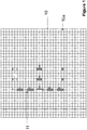
- Figure 1 is a top view of a display panel (10) comprising microcells (10a), on which a pre-patterned image "8" (11) appears.
- the display panel therefore has a patterned area (11) and a background area (i.e., area outside of the patterned area).
- FIG. 2 is a cross-section view of microcells (20). Each microcell has a bottom (21) and the microcells are filled with a display fluid (22). The inner surface or top surface (21a) of the bottom is in direct contact with the display fluid.
- microcell may be a cup-like micro-container as those described in US Patent No. 6,930,818 .
- Figure 3 is a cross-section view of microcells in a display panel of the present invention.
- the panel has a first area and a second area.
- first area refers to an area in which the microcells (30b) have substantially the same bottom thickness
- second area refers to an area in which the microcells (30a) have bottoms which are thicker than those in the microcells in the first area.
- substantially the same refers to variation in thickness being within manufacturing tolerance, for example, ⁇ 5%.
- the microcells (30a) in the second area have an added thickness "t", which may be in the range of 0.001 micron to 9/10 of the depth ("d") of the microcells in the first area (where the depths of the microcells are substantially uniform), preferably in the range of 0.001 micron to 1 ⁇ 2 of the depth of the microcells in the first area.
- the bottom thickness of the microcells in the second area is in the range of 0.001 micron to 9/10 of the depth of the microcells in the first area, preferably in the range of 0.001 micron to 1 ⁇ 2 of the depth of the microcells in the first area, more than the bottom thickness of the microcells in the first area.
- the second area may be a patterned area while the first area is a background area, or vice versa.
- the added bottom thicknesses in individual microcells in the second area do not have to be the same. Some of them may be thicker than the others.
- the display panel of the present invention may be prepared by a variety of methods.
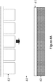
- FIGS 4A and 4B illustrate an embossing process as described in US Patent Nos. 6,831,770 and 6,930,818 .
- an embossable composition (40) is first coated over a substrate layer (41).
- the substrate layer is on a nip roller (42).
- a male mold (43) is pressed onto the embossable composition to form microcells (44).
- the embossable composition for forming the microcells may be hardened during or after the male mold is released. In this method, the microcells have substantially uniform bottom thickness.
- an electrode layer attached to the substrate layer (41).
- the embossable composition is coated on the electrode layer side.
- the electrode layer would be one of the two layers sandwiching the display panel in the final product.
- the substrate layer attached to the resulting display panel may be removed after the embossing process, and replaced with an electrode or another substrate layer.
- the method illustrated in Figures 4A and 4B is modified by carving out areas (55) on the nip roller (52) (see Figure 5 ) to form a pattern which may be a "positive" image or "negative” image of the intended pattern for the display panel.
- the pressure from the male mold exerted on the embossable composition in the carved-out areas is less than the pressure exerted on the embossable composition from the male mold in other areas.
- the bottoms of the microcells in the resulting display panel corresponding to the carved-out areas are thicker.
- the degree of the added thickness may be adjusted by altering the depth of the carved-out areas on the nip roller. A deeper carved out area on the nip roller would result in a thicker bottom of a microcell in the corresponding area.
- the term "positive image" referred to above indicates that the carved-out pattern on the nip roller is the same as the intended pattern for the display panel. In this case, the display panel formed would have a patterned area in which the microcells have thicker bottoms.
- negative image indicates that the carved-out pattern corresponds to an area excluding the intended pattern for the display panel.
- the display panel formed would have a background area in which the microcells have thicker bottoms.
- the surface of a nip roller is curved. However it is drawn as a straight line in Figures 4 and 5 , for illustration purpose only.
- the added thicknesses of the microcells do not have to be the same, which can be achieved by the method as described. In other words, variation in the depth of the carved-out areas on the nip roller will result in variation in the bottom thickness of the microcells.
- Suitable embossable compositions for forming the microcells are disclosed previously.
- US Patent Nos. 6,831,770 and 6,930,818 describe that a suitable composition for forming microcells may comprise a thermoplastic, thermoset, or a precursor thereof.
- thermoplastic or thermoset precursor may include multifunctional acrylate or methacrylate, multifunctional vinylether, multifunctional epoxide and oligomers or polymers thereof.
- a crosslinkable oligomer imparting flexibility, such as urethane acrylate or polyester acrylate, may also be added to improve the flexure resistance of the embossed microcells.
- US Patent No. 7,880,958 describes a further embossable composition for microcells which may comprise a polar oligomeric or polymeric material.
- a polar oligomeric or polymeric material may be selected from the group consisting of oligomers or polymers having at least one of the groups, such as nitro (-NO 2 ), hydroxyl (-OH), carboxyl (-COO), alkoxy (-OR wherein R is an alkyl group), halo (e.g., fluoro, chloro, bromo or iodo), cyano (-CN), sulfonate (-SO 3 ) and the like.
- the glass transition temperature of the polar polymer material is preferably below about 100°C and more preferably below about 60°C.
- suitable polar oligomeric or polymeric materials may include, but are not limited to, polyhydroxy functionalized polyester acrylates (such as BDE 1025, Bomar Specialties Co, Winsted, CT) or alkoxylated acrylates, such as ethoxylated nonyl phenol acrylate (e.g., SR504, Sartomer Company), ethoxylated trimethylolpropane triacrylate (e.g., SR9035, Sartomer Company) or ethoxylated pentaerythritol tetraacrylate (e.g., SR494, from Sartomer Company).
- polyhydroxy functionalized polyester acrylates such as BDE 1025, Bomar Specialties Co, Winsted, CT
- alkoxylated acrylates such as ethoxylated nonyl phenol acrylate (e.g., SR504, Sarto
- US Patent Application No. 13/686,778 discloses another type of embossable composition for forming microcells.
- the composition comprises (a) at least one difunctional UV curable component, (b) at least one photoinitiator, and (c) at least one mold release agent.
- Suitable difunctional components may have a molecular weight higher than about 200.
- Difunctional acrylates are preferred and difunctional acrylates having a urethane or ethoxylated backbone are particularly preferred.
- suitable difunctional components may include, but are not limited to, diethylene glycol diacrylate (e.g., SR230 from Sartomer), triethylene glycol diacrylate (e.g., SR272 from Sartomer), tetraethylene glycol diacrylate (e.g., SR268 from Sartomer), polyethylene glycol diacrylate (e.g., SR295, SR344 or SR610 from Sartomer), polyethylene glycol dimethacrylate (e.g., SR603, SR644, SR252 or SR740 from Sartomer), ethoxylated bisphenol A diacrylate (e.g., CD9038, SR349, SR601 or SR602 from Sartomer), ethoxylated bisphenol A dimethacrylate (e.g., CD540, CD542, SR101, SR150, SR348, SR480 or SR541 from Sartomer), and urethane diacrylate (e.g.,
- Suitable photoinitiators may include, but are not limited to, bis-acyl-phosphine oxide, 2-benzyl-2-(dimethylamino)-1-[4-(4-morpholinyl)phenyl]-1-butanone, 2,4,6-trimethylbenzoyl diphenyl phosphine oxide, 2-isopropyl-9H-thioxanthen-9-one, 4-benzoyl-4'-methyldiphenylsulphide and 1-hydroxy-cyclohexyl-phenyl-ketone, 2-hydroxy-2-methyl-1-phenyl-propan-1-one, 1-[4-(2-hydroxyethoxy)-phenyl]-2-hydroxy-2-methyl-1-propane-1-one, 2,2-dimethoxy-1,2-diphenylethan-1-one or 2-methyl-1[4-(methylthio)phenyl]-2-morpholinopropan-1-one.
- Suitable mold release agents may include, but are not limited to, organomodified silicone copolymers such as silicone acrylates (e.g., Ebercryl 1360 or Ebercyl 350 from Cytec), silicone polyethers (e.g., Silwet 7200, Silwet 7210, Silwet 7220, Silwet 7230, Silwet 7500, Silwet 7600 or Silwet 7607 from Momentive).
- the composition may further optionally comprise one or more of the following components, a co-initiator, monofunctional UV curable component, multifunctional UV curable component or stabilizer.
- the display panel of the present invention may be prepared as shown in Figure 6 .
- the microcells may be first prepared according to the method of Figures 4A and 4B .
- a chemical composition (61) is filled into the microcells in a pre-determined area (which may correspond to the patterned area or the background area on the display panel).
- the chemical composition contains a solid material dissolved or dispersed in a solvent that can be easily removed.
- the filling of the chemical composition in the pre-determined area may be accomplished by methods, such as inkjet printing or screen printing.
- the solid material may be a curable material, such as any of those described above for the embossing composition.
- the curing may be accomplished by known conventional methods, such as, thermal cure or radiation cure.
- the solid material may also be a material which does not need curing, such as polyurethane, poly(ethylene oxide), polystyrene, acrylate polymers [such as poly(methyl acrylate) and poly(butyl acrylate)] or methacrylate polymers [such as poly(methyl methacrylate) and poly(ethyl methacrylate)].
- polyurethane poly(ethylene oxide)
- polystyrene polystyrene
- acrylate polymers such as poly(methyl acrylate) and poly(butyl acrylate)
- methacrylate polymers such as poly(methyl methacrylate) and poly(ethyl methacrylate)
- the solid material in the chemical composition does not have to be the same as the embossable composition for forming the microcells.
- Suitable solvent for this method may include, but are not limited to, methyl ethyl ketone, acetone or isopropyl alcohol.
- the remaining solid material in the chemical composition should provide good adhesion to the bottom of the microcells and also does not inter-react with the display fluid to be filled in the microcells.
- the added thickness in the microcells is determined by the solid content in the chemical composition.
- the added thickness in the microcells may be determined by the concentration of the chemical composition.
- microcells may also be filled with chemical compositions with different concentrations, resulting in different bottom thicknesses.
- a display fluid is filled into the microcells.
- the display fluid may be an electrophoretic fluid which comprises charged particles dispersed in a solvent or solvent mixture.
- a display panel (70) with pre-determined images is sandwiched between two electrode layers (77 and 78), as shown in Figure 7 .
- an electrophoretic fluid may have one type of charged pigment particles dispersed in a solvent or solvent mixture of a contrasting color.
- the charged particles migrate by attraction to the plate of polarity opposite that of the particles.
- the color showing at the transparent plate may be either the color of the solvent or the color of the pigment particles. Reversal of plate polarity will cause the charged particles to migrate back to the opposite plate, thereby reversing the color.
- an electrophoretic fluid may have two types of charged particles of contrasting colors and carrying opposite charges, and the two types of pigment particles are dispersed in a clear solvent or solvent mixture.
- FIG. 8 illustrates one example of this phenomenon.
- the white particles in microcell A respond to the electric field created between electrode layers 87 and 88, and move to be near or at the electrode 87, and as a result, a white color is seen at the viewing side.
- microcell B in another area, because of the thicker bottom, the white particles sense a weaker electric field and as a result, a grey color is displayed.
- microcells may have different bottom thicknesses, different levels of color intensity (i.e., greyscale) are therefore possible.
- Figure 8 only demonstrates a design with only one type of charged particles, the phenomenon exhibited is applicable to electrophoretic fluids having any number of types of charged particles.
- both electrode layers are non-patterned conductive layers such as indium tin oxide, copper or aluminum,
- conductive layers such as indium tin oxide, copper or aluminum
- This design is particularly suitable for signage displays having fixed images, such as bar code, anti-counterfeiting labels, direction signage or shelf labels.
- one of the electrode layers is a common electrode while the other electrode layer is a TFT (thin film transistor) matrix driving system or segmented backplane driving system.
- the entire display panel may switch from one image to another image while one area remains to be distinguishable visually from another area.
- This embodiment of the present invention is particularly suitable as a watermark and the watermark does not interfere with the switching of the images.
- the inner surface of the microcells may be treated to modify its chemical functionality, morphology, microstructure, charge characteristics, surface tension or optical density.
- the surface may be treated with electron donating or proton accepting probe molecules or precursors thereof, including but are not limited to, ammonia, amines, imines, pyridines, ureas, thioureas, urethanes, pyrrolidones, imidazoles, ethers, thioethers, ketones, acrylates and acrylamides.
- the surface may be treated with electron accepting or proton donating probe molecules or precursors thereof, including but are not limited to, oxygen, carboxylic compounds, hydroxy containing compounds, acrylamides, silanols or organometallic compounds comprising an electron deficient center.
- Another option of surface treatment involves modification of the chemical functionality of the microcell surface by plasma or corona treatment to induce interaction between the charged pigment particles and the surface.
- One specific example is to modify the surface by plasma treatment using probe molecules having a functional group which is capable of forming a hydrogen bonding or acid-base reaction with a functional group on the surface of the dispersed particles.
- the hydrogen bonding may be formed from a proton donor or electron acceptor on the microcell surface and a proton acceptor or electron donor on the particles, or vice versa.
- the surface may be modified with plasma treatment to form a steric stabilization or protective colloid layer on the cell surface.
- the surface treatment of the microcells may be applied to all microcells or to only selected microcells, depending on the needs.
Landscapes
- Physics & Mathematics (AREA)
- Nonlinear Science (AREA)
- General Physics & Mathematics (AREA)
- Optics & Photonics (AREA)
- Chemical & Material Sciences (AREA)
- Life Sciences & Earth Sciences (AREA)
- Health & Medical Sciences (AREA)
- Molecular Biology (AREA)
- Electrochemistry (AREA)
- Chemical Kinetics & Catalysis (AREA)
- Engineering & Computer Science (AREA)
- Mathematical Physics (AREA)
- Crystallography & Structural Chemistry (AREA)
- Geometry (AREA)
- Computer Hardware Design (AREA)
- Theoretical Computer Science (AREA)
- Electrochromic Elements, Electrophoresis, Or Variable Reflection Or Absorption Elements (AREA)
- Devices For Indicating Variable Information By Combining Individual Elements (AREA)
- Credit Cards Or The Like (AREA)
Claims (15)
- Panneau d'affichage (10 ; 70) comprenant des microcellules (10a) remplies avec un fluide électrophorétique (22 ; 76), chacune des microcellules (10a) ayant la forme d'un microrécipient en forme de coupelle ayant une paroi inférieure (21), la surface interne (21a) de la paroi inférieure (21) étant en contact avec le fluide électrophorétique (22 ; 76), le panneau d'affichage (10) ayant une première zone et une deuxième zone (11), les microcellules (30b) dans la première zone ayant sensiblement la même épaisseur de paroi inférieure, et les microcellules (30a) dans la deuxième zone (11) ayant des parois inférieures plus épaisses que les microcellules (30b) dans la première zone, le panneau d'affichage (10 ; 70) étant caractérisé en ce que la deuxième zone (11) forme une image préformée, tandis que la première zone est une zone de fond, ou vice versa.
- Panneau de la revendication 1, dans lequel la différence d'épaisseur de paroi inférieure entre les microcellules (30a) dans la deuxième zone (11) et celles (30b) dans la première zone est de 0,001 micromètre à 9/10e de la profondeur des microcellules (30b) dans la première zone.
- Panneau de la revendication 2, dans lequel la différence d'épaisseur de paroi inférieure entre les microcellules (30a) dans la deuxième zone (11) et celles (30b) dans la première zone et de 0,001 micromètre à la moitié de la profondeur des microcellules (30b) dans la première zone.
- Panneau de la revendication 1, dans lequel les épaisseurs de paroi inférieure des microcellules (30a) dans la deuxième zone (11) varient.
- Panneau de la revendication 1, dans lequel le fluide électrophorétique (22 ; 76) remplissant les microcellules (30a, 30b) à la fois dans les première et deuxième (11) zones comprend un, deux ou plus de deux types de particules chargées dispersées dans un solvant ou mélange de solvants.
- Panneau de la revendication 1, qui est intercalé entre deux couches d'électrode (77, 78 ; 87, 88).
- Panneau de la revendication 6, dans lequel les deux couches d'électrode sont des couches conductrices sans motif (77, 78), ou une des couches d'électrode est une couche d'électrode commune et l'autre couche d'électrode est un système de commande à matrice de transistors en couche mince ou un système de commande à fond de panier segmenté.
- Panneau de la revendication 6, qui est utilisé dans des codes à barres, des étiquettes anti-contrefaçon, des panneaux de direction, des étiquettes de rayons ou une application de filigrane.
- Procédé de préparation du panneau d'affichage de la revendication 1, le procédé comprenant :a) l'obtention d'un rouleau pinceur (42) dont la surface a des zones détachées pour former un motif, lequel motif est une image positive ou négative d'un motif prévu pour le panneau d'affichage ;b) le dépôt d'une composition gaufrable (40) sur une couche de substrat (41) qui se trouve sur la surface du rouleau pinceur (42) ; etc) l'application d'un moule positif (43) sur la composition gaufrable (40).
- Procédé de la revendication 9, dans lequel les zones détachées varient en profondeur.
- Procédé de préparation du panneau d'affichage de la revendication 1, le procédé comprenant :a) l'obtention de microcellules (60) ;b) le remplissage des microcellules (60) dans une zone prédéterminée avec une composition chimique (61) dans un solvant ;c) le retrait du solvant ; etd) éventuellement, le durcissement de la composition chimique (61) après retrait du solvant.
- Procédé de la revendication 11, dans lequel le solvant est la méthyléthylcétone, l'acétone, ou l'alcool isopropylique.
- Procédé de la revendication 11, dans lequel les microcellules (60) sont remplies avec des compositions chimiques de différentes concentrations.
- Procédé de la revendication 13, dans lequel les concentrations se situent dans la gamme de 0,01 % à 90 % en poids.
- Procédé de la revendication 11, dans lequel la composition chimique (61) est identique à ou différente d'une composition dont sont formées les microcellules.
Applications Claiming Priority (2)
| Application Number | Priority Date | Filing Date | Title |
|---|---|---|---|
| US201361881346P | 2013-09-23 | 2013-09-23 | |
| PCT/US2014/055575 WO2015041969A1 (fr) | 2013-09-23 | 2014-09-15 | Panneau afficheur avec images pré-formées |
Publications (3)
| Publication Number | Publication Date |
|---|---|
| EP3049863A1 EP3049863A1 (fr) | 2016-08-03 |
| EP3049863A4 EP3049863A4 (fr) | 2017-06-07 |
| EP3049863B1 true EP3049863B1 (fr) | 2019-03-20 |
Family
ID=52689303
Family Applications (1)
| Application Number | Title | Priority Date | Filing Date |
|---|---|---|---|
| EP14846369.8A Active EP3049863B1 (fr) | 2013-09-23 | 2014-09-15 | Panneau afficheur avec images pré-formées |
Country Status (5)
| Country | Link |
|---|---|
| US (2) | US9436057B2 (fr) |
| EP (1) | EP3049863B1 (fr) |
| JP (2) | JP6285558B2 (fr) |
| TW (2) | TWI598673B (fr) |
| WO (1) | WO2015041969A1 (fr) |
Families Citing this family (24)
| Publication number | Priority date | Publication date | Assignee | Title |
|---|---|---|---|---|
| US10401668B2 (en) | 2012-05-30 | 2019-09-03 | E Ink California, Llc | Display device with visually-distinguishable watermark area and non-watermark area |
| EP3049863B1 (fr) * | 2013-09-23 | 2019-03-20 | E Ink California, LLC | Panneau afficheur avec images pré-formées |
| US10816868B2 (en) | 2013-09-23 | 2020-10-27 | E Ink California, Llc | Active molecule delivery system comprising microcells |
| US10802373B1 (en) | 2017-06-26 | 2020-10-13 | E Ink Corporation | Reflective microcells for electrophoretic displays and methods of making the same |
| US10921676B2 (en) | 2017-08-30 | 2021-02-16 | E Ink Corporation | Electrophoretic medium |
| US10698265B1 (en) | 2017-10-06 | 2020-06-30 | E Ink California, Llc | Quantum dot film |
| TWI774938B (zh) * | 2018-03-16 | 2022-08-21 | 美商電子墨水股份有限公司 | 電光顯示器的組合體 |
| JP7108779B2 (ja) | 2018-08-10 | 2022-07-28 | イー インク カリフォルニア, エルエルシー | 反射体を伴う切り替え可能な光コリメート層 |
| US11397366B2 (en) | 2018-08-10 | 2022-07-26 | E Ink California, Llc | Switchable light-collimating layer including bistable electrophoretic fluid |
| WO2020033031A1 (fr) * | 2018-08-10 | 2020-02-13 | E Ink California, Llc | Panneau d'affichage avec des images pré-échantillonnées |
| KR102521144B1 (ko) | 2018-08-10 | 2023-04-12 | 이 잉크 캘리포니아 엘엘씨 | 쌍안정 전기영동 유체를 포함하는 전환가능한 광 시준층에 대한 구동 파형들 |
| WO2022197654A1 (fr) * | 2021-03-15 | 2022-09-22 | E Ink Corporation | Modulateur de lumière commutable ayant des régions d'opacité variable |
| JP7688154B2 (ja) | 2021-04-16 | 2025-06-03 | イー インク コーポレイション | 薄型縁シールを伴う電気泳動ディスプレイ |
| JP2024536760A (ja) | 2021-09-16 | 2024-10-08 | イー インク コーポレイション | 改良された透過率を伴う切り替え可能な光コリメート層 |
| EP4433868A4 (fr) * | 2021-11-19 | 2025-11-12 | E Ink Corp | Dispositif d'affichage ayant un filigrane formé par des images en demi-teinte |
| US12479578B2 (en) | 2023-12-04 | 2025-11-25 | The Boeing Company | Active display interior vehicle surfaces |
| WO2025147410A2 (fr) | 2024-01-02 | 2025-07-10 | E Ink Corporation | Milieux électrophorétiques comprenant un agent de contrôle de charge cationique |
| US20250224645A1 (en) | 2024-01-05 | 2025-07-10 | E Ink Corporation | Electrophoretic medium comprising particles having a pigment core and a polymeric shell |
| US20250224646A1 (en) | 2024-01-08 | 2025-07-10 | E Ink Corporation | Adhesive Layer Comprising Conductive Filler Particles and a Polymeric Dispersant |
| WO2025230802A1 (fr) | 2024-04-30 | 2025-11-06 | E Ink Corporation | Dispositif de transmission de lumière variable comprenant des microcellules |
| US20250370306A1 (en) | 2024-05-30 | 2025-12-04 | E Ink Corporation | Chemically-Resistant Multi-Layered Electro-Optic Device and a Method of Making the Same |
| WO2026006117A1 (fr) | 2024-06-26 | 2026-01-02 | E Ink Corporation | Dispositif de transmission de lumière variable comprenant des microcellules |
| US20260003243A1 (en) | 2024-06-26 | 2026-01-01 | E Ink Corporation | Variable light transmission device comprising microcells |
| WO2026006119A1 (fr) | 2024-06-26 | 2026-01-02 | E Ink Corporation | Dispositif de transmission de lumière variable comprenant des microcellules |
Citations (1)
| Publication number | Priority date | Publication date | Assignee | Title |
|---|---|---|---|---|
| US20110133627A1 (en) * | 2009-12-09 | 2011-06-09 | Samsung Electro-Mechnics Co., Ltd. | Color electronic paper display device and method for manufacturing the same |
Family Cites Families (27)
| Publication number | Priority date | Publication date | Assignee | Title |
|---|---|---|---|---|
| US5384649A (en) * | 1991-12-26 | 1995-01-24 | Matsushita Electric Industrial Co., Ltd. | Liquid crystal spatial light modulator with electrically isolated reflecting films connected to electrically isolated pixel portions of photo conductor |
| US6930818B1 (en) | 2000-03-03 | 2005-08-16 | Sipix Imaging, Inc. | Electrophoretic display and novel process for its manufacture |
| US20070237962A1 (en) * | 2000-03-03 | 2007-10-11 | Rong-Chang Liang | Semi-finished display panels |
| US6831770B2 (en) | 2000-03-03 | 2004-12-14 | Sipix Imaging, Inc. | Electrophoretic display and novel process for its manufacture |
| US6822783B2 (en) * | 2001-06-26 | 2004-11-23 | Canon Kabushiki Kaisha | Electrophoretic display unit, and driving method thereof |
| JP2003084122A (ja) * | 2001-06-29 | 2003-03-19 | Koninkl Philips Electronics Nv | カラーフィルタ及びこれを用いた液晶表示装置並びにその製造方法 |
| TWI310098B (en) | 2002-05-03 | 2009-05-21 | Sipix Imaging Inc | Methods of surface modification for improving electrophoretic display performance |
| JP4168788B2 (ja) * | 2003-03-06 | 2008-10-22 | セイコーエプソン株式会社 | 成膜方法、カラーフィルタ基板の製造方法、エレクトロルミネッセンス装置用基板の製造方法、表示装置の製造方法 |
| US7206119B2 (en) * | 2003-12-31 | 2007-04-17 | E Ink Corporation | Electro-optic displays, and method for driving same |
| US7880958B2 (en) | 2005-09-23 | 2011-02-01 | Sipix Imaging, Inc. | Display cell structure and electrode protecting layer compositions |
| US20070205979A1 (en) | 2006-03-02 | 2007-09-06 | Bigelow Donald O | Electro-optical modulating display devices comprising and array of microcells and a method for making such devices |
| JP4816245B2 (ja) * | 2006-05-19 | 2011-11-16 | 株式会社日立製作所 | 電気泳動表示装置 |
| US7417787B2 (en) * | 2006-05-19 | 2008-08-26 | Xerox Corporation | Electrophoretic display device |
| US7713836B2 (en) * | 2006-09-29 | 2010-05-11 | Semiconductor Energy Laboratory Co., Ltd. | Method for forming conductive layer and substrate having the same, and method for manufacturing semiconductor device |
| JP2011014068A (ja) * | 2009-07-06 | 2011-01-20 | Toppan Forms Co Ltd | バーコード表示媒体 |
| US20110043543A1 (en) * | 2009-08-18 | 2011-02-24 | Hui Chen | Color tuning for electrophoretic display |
| KR20110028952A (ko) * | 2009-09-14 | 2011-03-22 | 삼성전기주식회사 | 전자 종이 표시장치 및 그 제조방법 |
| KR101089872B1 (ko) * | 2009-09-18 | 2011-12-05 | 삼성전기주식회사 | 전자종이 디스플레이 장치 및 제조방법 |
| KR20120076256A (ko) | 2010-12-29 | 2012-07-09 | 엘지디스플레이 주식회사 | 액정표시장치 |
| US8169691B1 (en) * | 2011-03-18 | 2012-05-01 | Toppan Printing Co., Ltd. | Multi color display panel |
| JP5741122B2 (ja) * | 2011-03-28 | 2015-07-01 | ソニー株式会社 | 電気泳動素子、表示装置および電子機器 |
| JP2013033125A (ja) | 2011-08-02 | 2013-02-14 | Seiko Epson Corp | 電気泳動表示シート、電気泳動表示装置及びその製造方法、並びに電子機器 |
| US9248013B2 (en) * | 2011-12-05 | 2016-02-02 | California Institute Of Technology | 3-Dimensional parylene scaffold cage |
| JP5516616B2 (ja) * | 2012-02-07 | 2014-06-11 | 日立化成株式会社 | 懸濁粒子装置及びこれを用いた調光装置並びにその駆動方法 |
| JP2013164538A (ja) | 2012-02-13 | 2013-08-22 | Fuji Xerox Co Ltd | 画像表示媒体 |
| US9388307B2 (en) | 2012-11-27 | 2016-07-12 | E Ink California, Llc | Microcup compositions |
| EP3049863B1 (fr) * | 2013-09-23 | 2019-03-20 | E Ink California, LLC | Panneau afficheur avec images pré-formées |
-
2014
- 2014-09-15 EP EP14846369.8A patent/EP3049863B1/fr active Active
- 2014-09-15 US US14/486,994 patent/US9436057B2/en active Active
- 2014-09-15 WO PCT/US2014/055575 patent/WO2015041969A1/fr not_active Ceased
- 2014-09-15 JP JP2016543941A patent/JP6285558B2/ja active Active
- 2014-09-22 TW TW105128073A patent/TWI598673B/zh active
- 2014-09-22 TW TW103132602A patent/TWI554815B/zh active
-
2016
- 2016-08-16 US US15/238,075 patent/US10073318B2/en active Active
-
2017
- 2017-08-04 JP JP2017151843A patent/JP6731384B2/ja active Active
Patent Citations (1)
| Publication number | Priority date | Publication date | Assignee | Title |
|---|---|---|---|---|
| US20110133627A1 (en) * | 2009-12-09 | 2011-06-09 | Samsung Electro-Mechnics Co., Ltd. | Color electronic paper display device and method for manufacturing the same |
Also Published As
| Publication number | Publication date |
|---|---|
| JP6731384B2 (ja) | 2020-07-29 |
| TWI598673B (zh) | 2017-09-11 |
| US20150085345A1 (en) | 2015-03-26 |
| US20160357084A1 (en) | 2016-12-08 |
| TWI554815B (zh) | 2016-10-21 |
| WO2015041969A1 (fr) | 2015-03-26 |
| JP2017207776A (ja) | 2017-11-24 |
| US9436057B2 (en) | 2016-09-06 |
| US10073318B2 (en) | 2018-09-11 |
| EP3049863A4 (fr) | 2017-06-07 |
| EP3049863A1 (fr) | 2016-08-03 |
| TW201520666A (zh) | 2015-06-01 |
| JP2016532163A (ja) | 2016-10-13 |
| TW201643534A (zh) | 2016-12-16 |
| JP6285558B2 (ja) | 2018-02-28 |
Similar Documents
| Publication | Publication Date | Title |
|---|---|---|
| EP3049863B1 (fr) | Panneau afficheur avec images pré-formées | |
| KR102521144B1 (ko) | 쌍안정 전기영동 유체를 포함하는 전환가능한 광 시준층에 대한 구동 파형들 | |
| US11656526B2 (en) | Switchable light-collimating layer including bistable electrophoretic fluid | |
| KR102521143B1 (ko) | 리플렉터를 갖는 전환가능한 광 시준층 | |
| EP3044631B1 (fr) | Film à affichage électrophorétique pour application anti-contrefaçon | |
| US12560836B2 (en) | Switchable light-collimating layer with improved transmittance | |
| US10816868B2 (en) | Active molecule delivery system comprising microcells | |
| CN112334825B (zh) | 具有预图案化图像的显示面板 | |
| HK40037037A (en) | Display panel with pre-patterened images | |
| HK40079043A (zh) | 包括双稳态电泳流体的可切换的光准直层 | |
| HK40038567A (en) | Switchable light-collimating layer including bistable electrophoretic fluid | |
| HK40038567B (zh) | 包括双稳态电泳流体的可切换的光准直层 |
Legal Events
| Date | Code | Title | Description |
|---|---|---|---|
| PUAI | Public reference made under article 153(3) epc to a published international application that has entered the european phase |
Free format text: ORIGINAL CODE: 0009012 |
|
| 17P | Request for examination filed |
Effective date: 20160425 |
|
| AK | Designated contracting states |
Kind code of ref document: A1 Designated state(s): AL AT BE BG CH CY CZ DE DK EE ES FI FR GB GR HR HU IE IS IT LI LT LU LV MC MK MT NL NO PL PT RO RS SE SI SK SM TR |
|
| AX | Request for extension of the european patent |
Extension state: BA ME |
|
| DAX | Request for extension of the european patent (deleted) | ||
| A4 | Supplementary search report drawn up and despatched |
Effective date: 20170508 |
|
| RIC1 | Information provided on ipc code assigned before grant |
Ipc: G02F 1/167 20060101AFI20170428BHEP |
|
| GRAP | Despatch of communication of intention to grant a patent |
Free format text: ORIGINAL CODE: EPIDOSNIGR1 |
|
| STAA | Information on the status of an ep patent application or granted ep patent |
Free format text: STATUS: GRANT OF PATENT IS INTENDED |
|
| INTG | Intention to grant announced |
Effective date: 20180919 |
|
| GRAS | Grant fee paid |
Free format text: ORIGINAL CODE: EPIDOSNIGR3 |
|
| GRAA | (expected) grant |
Free format text: ORIGINAL CODE: 0009210 |
|
| STAA | Information on the status of an ep patent application or granted ep patent |
Free format text: STATUS: THE PATENT HAS BEEN GRANTED |
|
| AK | Designated contracting states |
Kind code of ref document: B1 Designated state(s): AL AT BE BG CH CY CZ DE DK EE ES FI FR GB GR HR HU IE IS IT LI LT LU LV MC MK MT NL NO PL PT RO RS SE SI SK SM TR |
|
| REG | Reference to a national code |
Ref country code: GB Ref legal event code: FG4D |
|
| REG | Reference to a national code |
Ref country code: CH Ref legal event code: EP |
|
| REG | Reference to a national code |
Ref country code: DE Ref legal event code: R096 Ref document number: 602014043390 Country of ref document: DE |
|
| REG | Reference to a national code |
Ref country code: AT Ref legal event code: REF Ref document number: 1111123 Country of ref document: AT Kind code of ref document: T Effective date: 20190415 |
|
| REG | Reference to a national code |
Ref country code: IE Ref legal event code: FG4D |
|
| REG | Reference to a national code |
Ref country code: NL Ref legal event code: MP Effective date: 20190320 |
|
| PG25 | Lapsed in a contracting state [announced via postgrant information from national office to epo] |
Ref country code: LT Free format text: LAPSE BECAUSE OF FAILURE TO SUBMIT A TRANSLATION OF THE DESCRIPTION OR TO PAY THE FEE WITHIN THE PRESCRIBED TIME-LIMIT Effective date: 20190320 Ref country code: NO Free format text: LAPSE BECAUSE OF FAILURE TO SUBMIT A TRANSLATION OF THE DESCRIPTION OR TO PAY THE FEE WITHIN THE PRESCRIBED TIME-LIMIT Effective date: 20190620 Ref country code: SE Free format text: LAPSE BECAUSE OF FAILURE TO SUBMIT A TRANSLATION OF THE DESCRIPTION OR TO PAY THE FEE WITHIN THE PRESCRIBED TIME-LIMIT Effective date: 20190320 Ref country code: FI Free format text: LAPSE BECAUSE OF FAILURE TO SUBMIT A TRANSLATION OF THE DESCRIPTION OR TO PAY THE FEE WITHIN THE PRESCRIBED TIME-LIMIT Effective date: 20190320 |
|
| REG | Reference to a national code |
Ref country code: LT Ref legal event code: MG4D |
|
| PG25 | Lapsed in a contracting state [announced via postgrant information from national office to epo] |
Ref country code: NL Free format text: LAPSE BECAUSE OF FAILURE TO SUBMIT A TRANSLATION OF THE DESCRIPTION OR TO PAY THE FEE WITHIN THE PRESCRIBED TIME-LIMIT Effective date: 20190320 Ref country code: GR Free format text: LAPSE BECAUSE OF FAILURE TO SUBMIT A TRANSLATION OF THE DESCRIPTION OR TO PAY THE FEE WITHIN THE PRESCRIBED TIME-LIMIT Effective date: 20190621 Ref country code: HR Free format text: LAPSE BECAUSE OF FAILURE TO SUBMIT A TRANSLATION OF THE DESCRIPTION OR TO PAY THE FEE WITHIN THE PRESCRIBED TIME-LIMIT Effective date: 20190320 Ref country code: LV Free format text: LAPSE BECAUSE OF FAILURE TO SUBMIT A TRANSLATION OF THE DESCRIPTION OR TO PAY THE FEE WITHIN THE PRESCRIBED TIME-LIMIT Effective date: 20190320 Ref country code: BG Free format text: LAPSE BECAUSE OF FAILURE TO SUBMIT A TRANSLATION OF THE DESCRIPTION OR TO PAY THE FEE WITHIN THE PRESCRIBED TIME-LIMIT Effective date: 20190620 Ref country code: RS Free format text: LAPSE BECAUSE OF FAILURE TO SUBMIT A TRANSLATION OF THE DESCRIPTION OR TO PAY THE FEE WITHIN THE PRESCRIBED TIME-LIMIT Effective date: 20190320 |
|
| REG | Reference to a national code |
Ref country code: AT Ref legal event code: MK05 Ref document number: 1111123 Country of ref document: AT Kind code of ref document: T Effective date: 20190320 |
|
| PG25 | Lapsed in a contracting state [announced via postgrant information from national office to epo] |
Ref country code: AL Free format text: LAPSE BECAUSE OF FAILURE TO SUBMIT A TRANSLATION OF THE DESCRIPTION OR TO PAY THE FEE WITHIN THE PRESCRIBED TIME-LIMIT Effective date: 20190320 Ref country code: PT Free format text: LAPSE BECAUSE OF FAILURE TO SUBMIT A TRANSLATION OF THE DESCRIPTION OR TO PAY THE FEE WITHIN THE PRESCRIBED TIME-LIMIT Effective date: 20190720 Ref country code: ES Free format text: LAPSE BECAUSE OF FAILURE TO SUBMIT A TRANSLATION OF THE DESCRIPTION OR TO PAY THE FEE WITHIN THE PRESCRIBED TIME-LIMIT Effective date: 20190320 Ref country code: CZ Free format text: LAPSE BECAUSE OF FAILURE TO SUBMIT A TRANSLATION OF THE DESCRIPTION OR TO PAY THE FEE WITHIN THE PRESCRIBED TIME-LIMIT Effective date: 20190320 Ref country code: RO Free format text: LAPSE BECAUSE OF FAILURE TO SUBMIT A TRANSLATION OF THE DESCRIPTION OR TO PAY THE FEE WITHIN THE PRESCRIBED TIME-LIMIT Effective date: 20190320 Ref country code: EE Free format text: LAPSE BECAUSE OF FAILURE TO SUBMIT A TRANSLATION OF THE DESCRIPTION OR TO PAY THE FEE WITHIN THE PRESCRIBED TIME-LIMIT Effective date: 20190320 Ref country code: SK Free format text: LAPSE BECAUSE OF FAILURE TO SUBMIT A TRANSLATION OF THE DESCRIPTION OR TO PAY THE FEE WITHIN THE PRESCRIBED TIME-LIMIT Effective date: 20190320 |
|
| PG25 | Lapsed in a contracting state [announced via postgrant information from national office to epo] |
Ref country code: PL Free format text: LAPSE BECAUSE OF FAILURE TO SUBMIT A TRANSLATION OF THE DESCRIPTION OR TO PAY THE FEE WITHIN THE PRESCRIBED TIME-LIMIT Effective date: 20190320 Ref country code: SM Free format text: LAPSE BECAUSE OF FAILURE TO SUBMIT A TRANSLATION OF THE DESCRIPTION OR TO PAY THE FEE WITHIN THE PRESCRIBED TIME-LIMIT Effective date: 20190320 |
|
| PG25 | Lapsed in a contracting state [announced via postgrant information from national office to epo] |
Ref country code: IS Free format text: LAPSE BECAUSE OF FAILURE TO SUBMIT A TRANSLATION OF THE DESCRIPTION OR TO PAY THE FEE WITHIN THE PRESCRIBED TIME-LIMIT Effective date: 20190720 Ref country code: AT Free format text: LAPSE BECAUSE OF FAILURE TO SUBMIT A TRANSLATION OF THE DESCRIPTION OR TO PAY THE FEE WITHIN THE PRESCRIBED TIME-LIMIT Effective date: 20190320 |
|
| REG | Reference to a national code |
Ref country code: DE Ref legal event code: R097 Ref document number: 602014043390 Country of ref document: DE |
|
| PLBE | No opposition filed within time limit |
Free format text: ORIGINAL CODE: 0009261 |
|
| STAA | Information on the status of an ep patent application or granted ep patent |
Free format text: STATUS: NO OPPOSITION FILED WITHIN TIME LIMIT |
|
| PG25 | Lapsed in a contracting state [announced via postgrant information from national office to epo] |
Ref country code: DK Free format text: LAPSE BECAUSE OF FAILURE TO SUBMIT A TRANSLATION OF THE DESCRIPTION OR TO PAY THE FEE WITHIN THE PRESCRIBED TIME-LIMIT Effective date: 20190320 |
|
| 26N | No opposition filed |
Effective date: 20200102 |
|
| PG25 | Lapsed in a contracting state [announced via postgrant information from national office to epo] |
Ref country code: SI Free format text: LAPSE BECAUSE OF FAILURE TO SUBMIT A TRANSLATION OF THE DESCRIPTION OR TO PAY THE FEE WITHIN THE PRESCRIBED TIME-LIMIT Effective date: 20190320 |
|
| PG25 | Lapsed in a contracting state [announced via postgrant information from national office to epo] |
Ref country code: TR Free format text: LAPSE BECAUSE OF FAILURE TO SUBMIT A TRANSLATION OF THE DESCRIPTION OR TO PAY THE FEE WITHIN THE PRESCRIBED TIME-LIMIT Effective date: 20190320 |
|
| PG25 | Lapsed in a contracting state [announced via postgrant information from national office to epo] |
Ref country code: MC Free format text: LAPSE BECAUSE OF FAILURE TO SUBMIT A TRANSLATION OF THE DESCRIPTION OR TO PAY THE FEE WITHIN THE PRESCRIBED TIME-LIMIT Effective date: 20190320 |
|
| PG25 | Lapsed in a contracting state [announced via postgrant information from national office to epo] |
Ref country code: LU Free format text: LAPSE BECAUSE OF NON-PAYMENT OF DUE FEES Effective date: 20190915 Ref country code: IE Free format text: LAPSE BECAUSE OF NON-PAYMENT OF DUE FEES Effective date: 20190915 |
|
| REG | Reference to a national code |
Ref country code: BE Ref legal event code: MM Effective date: 20190930 |
|
| PG25 | Lapsed in a contracting state [announced via postgrant information from national office to epo] |
Ref country code: BE Free format text: LAPSE BECAUSE OF NON-PAYMENT OF DUE FEES Effective date: 20190930 |
|
| PG25 | Lapsed in a contracting state [announced via postgrant information from national office to epo] |
Ref country code: CY Free format text: LAPSE BECAUSE OF FAILURE TO SUBMIT A TRANSLATION OF THE DESCRIPTION OR TO PAY THE FEE WITHIN THE PRESCRIBED TIME-LIMIT Effective date: 20190320 |
|
| PG25 | Lapsed in a contracting state [announced via postgrant information from national office to epo] |
Ref country code: MT Free format text: LAPSE BECAUSE OF FAILURE TO SUBMIT A TRANSLATION OF THE DESCRIPTION OR TO PAY THE FEE WITHIN THE PRESCRIBED TIME-LIMIT Effective date: 20190320 Ref country code: HU Free format text: LAPSE BECAUSE OF FAILURE TO SUBMIT A TRANSLATION OF THE DESCRIPTION OR TO PAY THE FEE WITHIN THE PRESCRIBED TIME-LIMIT; INVALID AB INITIO Effective date: 20140915 |
|
| PG25 | Lapsed in a contracting state [announced via postgrant information from national office to epo] |
Ref country code: MK Free format text: LAPSE BECAUSE OF FAILURE TO SUBMIT A TRANSLATION OF THE DESCRIPTION OR TO PAY THE FEE WITHIN THE PRESCRIBED TIME-LIMIT Effective date: 20190320 |
|
| REG | Reference to a national code |
Ref country code: DE Ref legal event code: R081 Ref document number: 602014043390 Country of ref document: DE Owner name: E INK CORPORATION, BILLERICA, US Free format text: FORMER OWNER: E INK CALIFORNIA, LLC, FREMONT, CALIF., US |
|
| REG | Reference to a national code |
Ref country code: CH Ref legal event code: U11 Free format text: ST27 STATUS EVENT CODE: U-0-0-U10-U11 (AS PROVIDED BY THE NATIONAL OFFICE) Effective date: 20251001 |
|
| PGFP | Annual fee paid to national office [announced via postgrant information from national office to epo] |
Ref country code: DE Payment date: 20250820 Year of fee payment: 12 |
|
| PGFP | Annual fee paid to national office [announced via postgrant information from national office to epo] |
Ref country code: IT Payment date: 20250820 Year of fee payment: 12 |
|
| PGFP | Annual fee paid to national office [announced via postgrant information from national office to epo] |
Ref country code: GB Payment date: 20250820 Year of fee payment: 12 |
|
| PGFP | Annual fee paid to national office [announced via postgrant information from national office to epo] |
Ref country code: FR Payment date: 20250821 Year of fee payment: 12 |
|
| PGFP | Annual fee paid to national office [announced via postgrant information from national office to epo] |
Ref country code: CH Payment date: 20251001 Year of fee payment: 12 |