EP3051651A1 - Circuit de pontage d'interruptions de tension - Google Patents
Circuit de pontage d'interruptions de tension Download PDFInfo
- Publication number
- EP3051651A1 EP3051651A1 EP16000152.5A EP16000152A EP3051651A1 EP 3051651 A1 EP3051651 A1 EP 3051651A1 EP 16000152 A EP16000152 A EP 16000152A EP 3051651 A1 EP3051651 A1 EP 3051651A1
- Authority
- EP
- European Patent Office
- Prior art keywords
- diode
- voltage
- circuit arrangement
- arrangement according
- storage capacitor
- Prior art date
- Legal status (The legal status is an assumption and is not a legal conclusion. Google has not performed a legal analysis and makes no representation as to the accuracy of the status listed.)
- Granted
Links
Images


Classifications
-
- G—PHYSICS
- G01—MEASURING; TESTING
- G01D—MEASURING NOT SPECIALLY ADAPTED FOR A SPECIFIC VARIABLE; ARRANGEMENTS FOR MEASURING TWO OR MORE VARIABLES NOT COVERED IN A SINGLE OTHER SUBCLASS; TARIFF METERING APPARATUS; MEASURING OR TESTING NOT OTHERWISE PROVIDED FOR
- G01D4/00—Tariff metering apparatus
- G01D4/02—Details
-
- H—ELECTRICITY
- H02—GENERATION; CONVERSION OR DISTRIBUTION OF ELECTRIC POWER
- H02J—ELECTRIC POWER NETWORKS; CIRCUIT ARRANGEMENTS OR SYSTEMS FOR SUPPLYING OR DISTRIBUTING ELECTRIC POWER; SYSTEMS FOR STORING ELECTRIC ENERGY
- H02J1/00—Circuit arrangements for DC mains or DC distribution networks
- H02J1/10—Parallel operation of DC sources
- H02J1/12—Parallel operation of DC sources having power converters with further DC sources without power converters
-
- H—ELECTRICITY
- H02—GENERATION; CONVERSION OR DISTRIBUTION OF ELECTRIC POWER
- H02J—ELECTRIC POWER NETWORKS; CIRCUIT ARRANGEMENTS OR SYSTEMS FOR SUPPLYING OR DISTRIBUTING ELECTRIC POWER; SYSTEMS FOR STORING ELECTRIC ENERGY
- H02J9/00—Circuit arrangements for emergency or stand-by power supply, e.g. for emergency lighting
- H02J9/04—Circuit arrangements for emergency or stand-by power supply, e.g. for emergency lighting in which the distribution system is disconnected from the normal source and connected to a standby source
- H02J9/06—Circuit arrangements for emergency or stand-by power supply, e.g. for emergency lighting in which the distribution system is disconnected from the normal source and connected to a standby source with automatic change-over, e.g. UPS systems
- H02J9/061—Circuit arrangements for emergency or stand-by power supply, e.g. for emergency lighting in which the distribution system is disconnected from the normal source and connected to a standby source with automatic change-over, e.g. UPS systems for DC powered loads
-
- G—PHYSICS
- G01—MEASURING; TESTING
- G01R—MEASURING ELECTRIC VARIABLES; MEASURING MAGNETIC VARIABLES
- G01R22/00—Arrangements for measuring time integral of electric power or current, e.g. electricity meters
Definitions
- the invention relates to a circuit arrangement for bridging power interruptions of connected to an electrical supply network electronic devices according to claim 1 and a use of the circuit arrangement in a unit for detecting physical quantities, in particular in an electronic consumption meter, for example in an electronic heat meter, water meter, energy meter , electronic electricity meter or gas meter for detecting amounts of energy or fluid and / or their also retrofittable communication modules.
- Such SMPS have a pre-stage, which converts an applied AC voltage (AC) into a DC voltage (DC) to generate a different voltage level or a galvanically isolated voltage from the generated DC voltage in a downstream converter stage.
- AC AC voltage
- DC DC voltage
- the conversion of the AC voltage to a DC voltage is typically achieved by means of rectifier circuits constructed from single-throw rectifiers or bridge rectifiers.
- the disadvantage here is that from a power consumption of about 500 watts, a power factor compensation is necessary, which can not be realized with the known diode technology.
- the rectified voltage are usually followed by energy storage, which are preferably constructed of electrolytic capacitors with a relatively high capacitance and may only be operated with DC voltage.
- energy storage which are preferably constructed of electrolytic capacitors with a relatively high capacitance and may only be operated with DC voltage.
- electrolytic capacitors have a maximum electrical voltage compatibility of about 450V and are thus theoretically applicable for rectified voltages of up to 320Vrms. Thereafter, an electrical breakdown of the insulating electrolyte and the capacitors are destroyed.
- the switched-mode power supply units with rectifier circuits are therefore operated with a supply voltage of> 276 Vrms (results from a voltage increase of 20% for a 230 V operation), it is necessary to prevent the maximum voltage at the capacitors from being exceeded.
- a single capacitor can be preceded by a linear regulator, wherein the capacitor can be charged up to a defined voltage level and the entire capacitance of the capacitor can be used.
- a current flows through the linear regulator, which converts a non-negligible power loss into heat.
- the invention has for its object to provide a circuit arrangement for bridging voltage interruptions of connected to an electrical supply network electronic devices, whereby the aforementioned disadvantages of the prior art are overcome.
- the inventive circuit arrangement for bridging voltage interruptions is composed of two series-connected capacitors, which form a capacitive voltage divider, one of the capacitors, which operates as a storage capacitor, with a linear voltage regulator, also called linear regulator, and a discharge diode or freewheeling diode is connected.
- the storage capacitor is equipped with a capacity that allows it to work as a storage capacitor (buffer / buffer capacitor).
- the other capacitor is connected in parallel with the linear regulator input and the linear regulator output, so that this capacitor prevents recharging of the storage capacitor by the linear regulator.
- the heat-generating power loss is reduced in an advantageous manner in the linear regulator.
- the voltage regulator is constructed from a MOSFET transistor as a source follower.
- the charging voltage of the storage capacitor is adjustable by the voltage drop across the reference voltage diode.
- An Avalange diode arranged within the MOSFET transistor operates as a freewheeling diode during a power interruption.
- the charging voltage of the storage capacitor can be adjustable for example by means of a zener diode, suppressor diode or a varistor.
- a Zener diode or a suppressor diode may be provided, which limits the voltage between the gate and source of the MOSFET transistor.
- the between the series resistor, the zener diode or the suppressor diode for adjusting the charging voltage of the storage capacitor and the gate of the MOSFET transistor-connected discharge protection diode may be replaced by a short-circuit connection, wherein in this advantageous embodiment, the resistance to accelerate the Blocking behavior of the MOSFET transistor is eliminated.
- circuit arrangement according to the invention are executed as Suppressordiode gate protection diode and the suppressor diode for adjusting the charging voltage of the storage capacitor by appropriately dimention convinced Zener diodes replaced and the gate protection diode, the discharge-protection diode is connected in the reverse direction.
- the voltage which determines the voltage for the storage capacitor can be set by means of a suppressor diode.
- the circuit arrangement according to the invention is arranged in the supply network of a consumption meter.
- Fig. 1 shows an exemplary block diagram of the circuit arrangement according to the invention for bridging voltage interruptions of an electronic device connected to an electrical supply network.
- the circuit arrangement according to the invention is connected to the supply voltage of an electronic device connected to an electrical supply network, preferably a consumption meter, and comprises two series-connected capacitors C1, C2, which form a capacitive voltage divider 30, one of the capacitors C2, which operates as a storage capacitor, is connected in parallel with a linear voltage regulator 10 and a discharge diode 20 and the other capacitor C1, also called Brumm capacitor, the linear regulator input E and the linear regulator output A of the voltage regulator 10 is connected in parallel, so that this capacitor C1, the 50th / 60 HZ prevents pulsating recharging of the storage capacitor C2 by the linear regulator 10.
- an electrical supply network preferably a consumption meter
- the capacitor C1 has a low capacitance (e.g., 6.8 ⁇ F).
- the storage capacitor C2 is designed as a high-capacitance storage capacitor (e.g., 68 ⁇ F) whose electrical storage capacity is significantly higher than conventional capacitors.
- the storage capacitor is at a lower voltage than the capacitor C1.
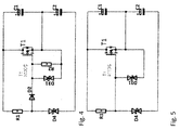
- Fig. 2 shows a first exemplary embodiment of the circuit arrangement according to the invention, which comprises the capacitors C1 and C2, which form the capacitive voltage divider 30.
- the linear regulator 10 is constructed of a MOSFET transistor T1, a Zener diode D1 and a series resistor R1.
- the charging voltage of the storage capacitor C2 is set by the voltage drop across the zener diode D1.
- the Avalange diode disposed within the MOSFET transistor T1 operates as a freewheeling diode during a power interruption.
- the gate of the MOSFET transistor T1 is preceded by a further Zener diode D3 as a reverse-acting gate protection diode.
- the further Zener diode D3 is connected in parallel with a resistor R2.
- the resistor R2 accelerates the blocking behavior of the MOSFET transistor T1.
- the Zener diode D1 which sets the charging voltage of the storage capacitor C2, by a suppressor diode D4, as a transient absorption Zener diode (TAZ diode) or Transient Voltage Suppressor Diode (TVS diode) called diode known replaced.
- TTZ diode transient absorption Zener diode
- TVS diode Transient Voltage Suppressor Diode
- the Zener diode D1 or the suppressor diode D4 and the gate of the MOSFET transistor T1 intermediate discharge protection diode D2 is replaced by a short circuit connection.
- the in the Fig. 1 - 4th provided resistor R2 to accelerate the blocking behavior of the MOSFET transistor T1 is eliminated.
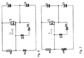
- Fig. 6 shows an embodiment of the circuit arrangement according to the invention, wherein the two in the Fig. 5 shown suppressor diodes D4, D31 are replaced by Zener diodes D1, D3.
- the discharge protection diode D2 is connected downstream of the gate protection diode D3 in the reverse direction.
- Fig. 7 is another exemplary embodiment of the circuit arrangement according to the invention, wherein in the Fig. 6 illustrated circuit modified to the effect has been that the voltage for the storage capacitor C2 voltage-determining voltage is set by a suppressor diode D4.
- the circuit according to the invention is not on the in the FIGS. 2 to 7 limited embodiments described. There are also other combinations of the circuits shown there are possible.
Landscapes
- Engineering & Computer Science (AREA)
- Power Engineering (AREA)
- Business, Economics & Management (AREA)
- Emergency Management (AREA)
- Physics & Mathematics (AREA)
- General Physics & Mathematics (AREA)
- Direct Current Feeding And Distribution (AREA)
- Stand-By Power Supply Arrangements (AREA)
Applications Claiming Priority (1)
| Application Number | Priority Date | Filing Date | Title |
|---|---|---|---|
| DE201520000662 DE202015000662U1 (de) | 2015-01-29 | 2015-01-29 | Schaltungsanordnung zur Überbrückung von Spannungsunterbrechungen |
Publications (2)
| Publication Number | Publication Date |
|---|---|
| EP3051651A1 true EP3051651A1 (fr) | 2016-08-03 |
| EP3051651B1 EP3051651B1 (fr) | 2018-07-11 |
Family
ID=52738461
Family Applications (1)
| Application Number | Title | Priority Date | Filing Date |
|---|---|---|---|
| EP16000152.5A Active EP3051651B1 (fr) | 2015-01-29 | 2016-01-22 | Circuit de pontage d'interruptions de tension |
Country Status (2)
| Country | Link |
|---|---|
| EP (1) | EP3051651B1 (fr) |
| DE (1) | DE202015000662U1 (fr) |
Cited By (1)
| Publication number | Priority date | Publication date | Assignee | Title |
|---|---|---|---|---|
| CN108733117A (zh) * | 2018-04-28 | 2018-11-02 | 北京机械设备研究所 | 一种伺服机构电源远端稳压的线路压降控制装置 |
Citations (2)
| Publication number | Priority date | Publication date | Assignee | Title |
|---|---|---|---|---|
| US20100090663A1 (en) * | 2008-10-10 | 2010-04-15 | Pappas Alexander N | Energy storage module |
| US20140266073A1 (en) * | 2013-03-15 | 2014-09-18 | Silver Spring Networks | Energy storage circuit |
-
2015
- 2015-01-29 DE DE201520000662 patent/DE202015000662U1/de not_active Expired - Lifetime
-
2016
- 2016-01-22 EP EP16000152.5A patent/EP3051651B1/fr active Active
Patent Citations (2)
| Publication number | Priority date | Publication date | Assignee | Title |
|---|---|---|---|---|
| US20100090663A1 (en) * | 2008-10-10 | 2010-04-15 | Pappas Alexander N | Energy storage module |
| US20140266073A1 (en) * | 2013-03-15 | 2014-09-18 | Silver Spring Networks | Energy storage circuit |
Cited By (1)
| Publication number | Priority date | Publication date | Assignee | Title |
|---|---|---|---|---|
| CN108733117A (zh) * | 2018-04-28 | 2018-11-02 | 北京机械设备研究所 | 一种伺服机构电源远端稳压的线路压降控制装置 |
Also Published As
| Publication number | Publication date |
|---|---|
| DE202015000662U1 (de) | 2015-03-05 |
| EP3051651B1 (fr) | 2018-07-11 |
Similar Documents
| Publication | Publication Date | Title |
|---|---|---|
| DE69712243T2 (de) | Universeller Leistungsmodul | |
| DE102009052461A1 (de) | Wechselrichter-Schaltungsanordnung | |
| DE102005002360B4 (de) | Tiefsetzer, Verfahren zur Ansteuerung und Verwendung des Tiefsetzers | |
| EP2026457A1 (fr) | Onduleur avec deux circuits intermédiaires | |
| DE102012216691A1 (de) | Stromrichterschaltung und Verfahren zur Steuerung der Stromrichterschaltung | |
| DE102022111107A1 (de) | Energieversorgungsvorrichtung für eine Elektrolyseeinheit und Elektrolyseanlage | |
| DE102009029843A1 (de) | Netzfilter und Verwendung eines Netzfilters | |
| DE102018125272A1 (de) | Vorrichtung und Verfahren zum Entladen eines Zwischenkreiskondensators, Stromrichter und Fahrzeug | |
| DE102015207605A1 (de) | Gleichspannungswandler | |
| EP0057910B2 (fr) | Circuit pour l'alimentation régulée d'un utilisateur | |
| DE102014109048B4 (de) | Schaltungsanordnung mit einer Mehrfachniveau-Halbbrückenanordnung | |
| EP3051651B1 (fr) | Circuit de pontage d'interruptions de tension | |
| DE102016220679A1 (de) | Gleichspannungswandler und Verfahren zur Ansteuerung eines Gleichspannungswandlers | |
| EP1867035B1 (fr) | Procède de fonctionnement d'une alimentation a découpage avec récupération d'énergie de diffusion cote primaire | |
| EP3602762A1 (fr) | Onduleur | |
| DE102017203233A1 (de) | Modularer Wechselrichter | |
| DE102004061341A1 (de) | Stromversorgung | |
| EP0357060A2 (fr) | Dispositif de protection contre la surtension pour un circuit électronique | |
| DE19841972A1 (de) | Getakteter Shuntregler | |
| AT405228B (de) | Netzgleichrichterschaltung | |
| DE102015115481A1 (de) | Schaltnetzteilvorrichtung | |
| DE20203714U1 (de) | Schaltnetzteil, insbesondere für medizinische Geräte | |
| DE102004020792B4 (de) | Elektrischer Schaltwandler mit hoher Eingangsspannung | |
| DE112014006555B4 (de) | Kommutierungsschaltung | |
| DE102013207894A1 (de) | Elektrische Schaltung |
Legal Events
| Date | Code | Title | Description |
|---|---|---|---|
| PUAI | Public reference made under article 153(3) epc to a published international application that has entered the european phase |
Free format text: ORIGINAL CODE: 0009012 |
|
| AK | Designated contracting states |
Kind code of ref document: A1 Designated state(s): AL AT BE BG CH CY CZ DE DK EE ES FI FR GB GR HR HU IE IS IT LI LT LU LV MC MK MT NL NO PL PT RO RS SE SI SK SM TR |
|
| AX | Request for extension of the european patent |
Extension state: BA ME |
|
| 17P | Request for examination filed |
Effective date: 20160913 |
|
| GRAP | Despatch of communication of intention to grant a patent |
Free format text: ORIGINAL CODE: EPIDOSNIGR1 |
|
| STAA | Information on the status of an ep patent application or granted ep patent |
Free format text: STATUS: GRANT OF PATENT IS INTENDED |
|
| INTG | Intention to grant announced |
Effective date: 20180405 |
|
| GRAS | Grant fee paid |
Free format text: ORIGINAL CODE: EPIDOSNIGR3 |
|
| GRAA | (expected) grant |
Free format text: ORIGINAL CODE: 0009210 |
|
| STAA | Information on the status of an ep patent application or granted ep patent |
Free format text: STATUS: THE PATENT HAS BEEN GRANTED |
|
| AK | Designated contracting states |
Kind code of ref document: B1 Designated state(s): AL AT BE BG CH CY CZ DE DK EE ES FI FR GB GR HR HU IE IS IT LI LT LU LV MC MK MT NL NO PL PT RO RS SE SI SK SM TR |
|
| REG | Reference to a national code |
Ref country code: GB Ref legal event code: FG4D Free format text: NOT ENGLISH |
|
| REG | Reference to a national code |
Ref country code: CH Ref legal event code: EP |
|
| REG | Reference to a national code |
Ref country code: AT Ref legal event code: REF Ref document number: 1017916 Country of ref document: AT Kind code of ref document: T Effective date: 20180715 |
|
| REG | Reference to a national code |
Ref country code: IE Ref legal event code: FG4D Free format text: LANGUAGE OF EP DOCUMENT: GERMAN |
|
| REG | Reference to a national code |
Ref country code: DE Ref legal event code: R096 Ref document number: 502016001411 Country of ref document: DE |
|
| REG | Reference to a national code |
Ref country code: NL Ref legal event code: MP Effective date: 20180711 |
|
| REG | Reference to a national code |
Ref country code: LT Ref legal event code: MG4D |
|
| PG25 | Lapsed in a contracting state [announced via postgrant information from national office to epo] |
Ref country code: NL Free format text: LAPSE BECAUSE OF FAILURE TO SUBMIT A TRANSLATION OF THE DESCRIPTION OR TO PAY THE FEE WITHIN THE PRESCRIBED TIME-LIMIT Effective date: 20180711 |
|
| PG25 | Lapsed in a contracting state [announced via postgrant information from national office to epo] |
Ref country code: FI Free format text: LAPSE BECAUSE OF FAILURE TO SUBMIT A TRANSLATION OF THE DESCRIPTION OR TO PAY THE FEE WITHIN THE PRESCRIBED TIME-LIMIT Effective date: 20180711 Ref country code: LT Free format text: LAPSE BECAUSE OF FAILURE TO SUBMIT A TRANSLATION OF THE DESCRIPTION OR TO PAY THE FEE WITHIN THE PRESCRIBED TIME-LIMIT Effective date: 20180711 Ref country code: PL Free format text: LAPSE BECAUSE OF FAILURE TO SUBMIT A TRANSLATION OF THE DESCRIPTION OR TO PAY THE FEE WITHIN THE PRESCRIBED TIME-LIMIT Effective date: 20180711 Ref country code: NO Free format text: LAPSE BECAUSE OF FAILURE TO SUBMIT A TRANSLATION OF THE DESCRIPTION OR TO PAY THE FEE WITHIN THE PRESCRIBED TIME-LIMIT Effective date: 20181011 Ref country code: SE Free format text: LAPSE BECAUSE OF FAILURE TO SUBMIT A TRANSLATION OF THE DESCRIPTION OR TO PAY THE FEE WITHIN THE PRESCRIBED TIME-LIMIT Effective date: 20180711 Ref country code: BG Free format text: LAPSE BECAUSE OF FAILURE TO SUBMIT A TRANSLATION OF THE DESCRIPTION OR TO PAY THE FEE WITHIN THE PRESCRIBED TIME-LIMIT Effective date: 20181011 Ref country code: IS Free format text: LAPSE BECAUSE OF FAILURE TO SUBMIT A TRANSLATION OF THE DESCRIPTION OR TO PAY THE FEE WITHIN THE PRESCRIBED TIME-LIMIT Effective date: 20181111 Ref country code: RS Free format text: LAPSE BECAUSE OF FAILURE TO SUBMIT A TRANSLATION OF THE DESCRIPTION OR TO PAY THE FEE WITHIN THE PRESCRIBED TIME-LIMIT Effective date: 20180711 Ref country code: GR Free format text: LAPSE BECAUSE OF FAILURE TO SUBMIT A TRANSLATION OF THE DESCRIPTION OR TO PAY THE FEE WITHIN THE PRESCRIBED TIME-LIMIT Effective date: 20181012 |
|
| PG25 | Lapsed in a contracting state [announced via postgrant information from national office to epo] |
Ref country code: HR Free format text: LAPSE BECAUSE OF FAILURE TO SUBMIT A TRANSLATION OF THE DESCRIPTION OR TO PAY THE FEE WITHIN THE PRESCRIBED TIME-LIMIT Effective date: 20180711 Ref country code: LV Free format text: LAPSE BECAUSE OF FAILURE TO SUBMIT A TRANSLATION OF THE DESCRIPTION OR TO PAY THE FEE WITHIN THE PRESCRIBED TIME-LIMIT Effective date: 20180711 Ref country code: AL Free format text: LAPSE BECAUSE OF FAILURE TO SUBMIT A TRANSLATION OF THE DESCRIPTION OR TO PAY THE FEE WITHIN THE PRESCRIBED TIME-LIMIT Effective date: 20180711 |
|
| REG | Reference to a national code |
Ref country code: DE Ref legal event code: R097 Ref document number: 502016001411 Country of ref document: DE |
|
| PG25 | Lapsed in a contracting state [announced via postgrant information from national office to epo] |
Ref country code: ES Free format text: LAPSE BECAUSE OF FAILURE TO SUBMIT A TRANSLATION OF THE DESCRIPTION OR TO PAY THE FEE WITHIN THE PRESCRIBED TIME-LIMIT Effective date: 20180711 Ref country code: CZ Free format text: LAPSE BECAUSE OF FAILURE TO SUBMIT A TRANSLATION OF THE DESCRIPTION OR TO PAY THE FEE WITHIN THE PRESCRIBED TIME-LIMIT Effective date: 20180711 Ref country code: IT Free format text: LAPSE BECAUSE OF FAILURE TO SUBMIT A TRANSLATION OF THE DESCRIPTION OR TO PAY THE FEE WITHIN THE PRESCRIBED TIME-LIMIT Effective date: 20180711 Ref country code: EE Free format text: LAPSE BECAUSE OF FAILURE TO SUBMIT A TRANSLATION OF THE DESCRIPTION OR TO PAY THE FEE WITHIN THE PRESCRIBED TIME-LIMIT Effective date: 20180711 Ref country code: RO Free format text: LAPSE BECAUSE OF FAILURE TO SUBMIT A TRANSLATION OF THE DESCRIPTION OR TO PAY THE FEE WITHIN THE PRESCRIBED TIME-LIMIT Effective date: 20180711 |
|
| PLBE | No opposition filed within time limit |
Free format text: ORIGINAL CODE: 0009261 |
|
| STAA | Information on the status of an ep patent application or granted ep patent |
Free format text: STATUS: NO OPPOSITION FILED WITHIN TIME LIMIT |
|
| PG25 | Lapsed in a contracting state [announced via postgrant information from national office to epo] |
Ref country code: SK Free format text: LAPSE BECAUSE OF FAILURE TO SUBMIT A TRANSLATION OF THE DESCRIPTION OR TO PAY THE FEE WITHIN THE PRESCRIBED TIME-LIMIT Effective date: 20180711 Ref country code: SM Free format text: LAPSE BECAUSE OF FAILURE TO SUBMIT A TRANSLATION OF THE DESCRIPTION OR TO PAY THE FEE WITHIN THE PRESCRIBED TIME-LIMIT Effective date: 20180711 Ref country code: DK Free format text: LAPSE BECAUSE OF FAILURE TO SUBMIT A TRANSLATION OF THE DESCRIPTION OR TO PAY THE FEE WITHIN THE PRESCRIBED TIME-LIMIT Effective date: 20180711 |
|
| 26N | No opposition filed |
Effective date: 20190412 |
|
| PG25 | Lapsed in a contracting state [announced via postgrant information from national office to epo] |
Ref country code: MC Free format text: LAPSE BECAUSE OF FAILURE TO SUBMIT A TRANSLATION OF THE DESCRIPTION OR TO PAY THE FEE WITHIN THE PRESCRIBED TIME-LIMIT Effective date: 20180711 Ref country code: SI Free format text: LAPSE BECAUSE OF FAILURE TO SUBMIT A TRANSLATION OF THE DESCRIPTION OR TO PAY THE FEE WITHIN THE PRESCRIBED TIME-LIMIT Effective date: 20180711 |
|
| PG25 | Lapsed in a contracting state [announced via postgrant information from national office to epo] |
Ref country code: LU Free format text: LAPSE BECAUSE OF NON-PAYMENT OF DUE FEES Effective date: 20190122 |
|
| REG | Reference to a national code |
Ref country code: BE Ref legal event code: MM Effective date: 20190131 |
|
| REG | Reference to a national code |
Ref country code: IE Ref legal event code: MM4A |
|
| PG25 | Lapsed in a contracting state [announced via postgrant information from national office to epo] |
Ref country code: BE Free format text: LAPSE BECAUSE OF NON-PAYMENT OF DUE FEES Effective date: 20190131 |
|
| PG25 | Lapsed in a contracting state [announced via postgrant information from national office to epo] |
Ref country code: IE Free format text: LAPSE BECAUSE OF NON-PAYMENT OF DUE FEES Effective date: 20190122 |
|
| PG25 | Lapsed in a contracting state [announced via postgrant information from national office to epo] |
Ref country code: TR Free format text: LAPSE BECAUSE OF FAILURE TO SUBMIT A TRANSLATION OF THE DESCRIPTION OR TO PAY THE FEE WITHIN THE PRESCRIBED TIME-LIMIT Effective date: 20180711 |
|
| PG25 | Lapsed in a contracting state [announced via postgrant information from national office to epo] |
Ref country code: MT Free format text: LAPSE BECAUSE OF FAILURE TO SUBMIT A TRANSLATION OF THE DESCRIPTION OR TO PAY THE FEE WITHIN THE PRESCRIBED TIME-LIMIT Effective date: 20180711 Ref country code: PT Free format text: LAPSE BECAUSE OF FAILURE TO SUBMIT A TRANSLATION OF THE DESCRIPTION OR TO PAY THE FEE WITHIN THE PRESCRIBED TIME-LIMIT Effective date: 20181111 |
|
| PG25 | Lapsed in a contracting state [announced via postgrant information from national office to epo] |
Ref country code: CY Free format text: LAPSE BECAUSE OF FAILURE TO SUBMIT A TRANSLATION OF THE DESCRIPTION OR TO PAY THE FEE WITHIN THE PRESCRIBED TIME-LIMIT Effective date: 20180711 |
|
| PG25 | Lapsed in a contracting state [announced via postgrant information from national office to epo] |
Ref country code: HU Free format text: LAPSE BECAUSE OF FAILURE TO SUBMIT A TRANSLATION OF THE DESCRIPTION OR TO PAY THE FEE WITHIN THE PRESCRIBED TIME-LIMIT; INVALID AB INITIO Effective date: 20160122 |
|
| PG25 | Lapsed in a contracting state [announced via postgrant information from national office to epo] |
Ref country code: MK Free format text: LAPSE BECAUSE OF FAILURE TO SUBMIT A TRANSLATION OF THE DESCRIPTION OR TO PAY THE FEE WITHIN THE PRESCRIBED TIME-LIMIT Effective date: 20180711 |
|
| P01 | Opt-out of the competence of the unified patent court (upc) registered |
Effective date: 20230414 |
|
| REG | Reference to a national code |
Ref country code: CH Ref legal event code: U11 Free format text: ST27 STATUS EVENT CODE: U-0-0-U10-U11 (AS PROVIDED BY THE NATIONAL OFFICE) Effective date: 20260201 |
|
| PGFP | Annual fee paid to national office [announced via postgrant information from national office to epo] |
Ref country code: GB Payment date: 20260126 Year of fee payment: 11 |
|
| PGFP | Annual fee paid to national office [announced via postgrant information from national office to epo] |
Ref country code: DE Payment date: 20260127 Year of fee payment: 11 |
|
| PGFP | Annual fee paid to national office [announced via postgrant information from national office to epo] |
Ref country code: AT Payment date: 20260119 Year of fee payment: 11 |
|
| PGFP | Annual fee paid to national office [announced via postgrant information from national office to epo] |
Ref country code: FR Payment date: 20260127 Year of fee payment: 11 |
|
| PGFP | Annual fee paid to national office [announced via postgrant information from national office to epo] |
Ref country code: CH Payment date: 20260201 Year of fee payment: 11 |