EP3053266B1 - Utilisations de traitements informatiques de retards fractionnels pour améliorer des performances d'intermodulation - Google Patents
Utilisations de traitements informatiques de retards fractionnels pour améliorer des performances d'intermodulation Download PDFInfo
- Publication number
- EP3053266B1 EP3053266B1 EP14850285.9A EP14850285A EP3053266B1 EP 3053266 B1 EP3053266 B1 EP 3053266B1 EP 14850285 A EP14850285 A EP 14850285A EP 3053266 B1 EP3053266 B1 EP 3053266B1
- Authority
- EP
- European Patent Office
- Prior art keywords
- signal waveform
- subsequent
- fractional delay
- fractional
- transmitted signal
- Prior art date
- Legal status (The legal status is an assumption and is not a legal conclusion. Google has not performed a legal analysis and makes no representation as to the accuracy of the status listed.)
- Active
Links
Images




Classifications
-
- H—ELECTRICITY
- H03—ELECTRONIC CIRCUITRY
- H03F—AMPLIFIERS
- H03F1/00—Details of amplifiers with only discharge tubes, only semiconductor devices or only unspecified devices as amplifying elements
- H03F1/32—Modifications of amplifiers to reduce non-linear distortion
- H03F1/3241—Modifications of amplifiers to reduce non-linear distortion using predistortion circuits
- H03F1/3247—Modifications of amplifiers to reduce non-linear distortion using predistortion circuits using feedback acting on predistortion circuits
-
- H—ELECTRICITY
- H03—ELECTRONIC CIRCUITRY
- H03F—AMPLIFIERS
- H03F1/00—Details of amplifiers with only discharge tubes, only semiconductor devices or only unspecified devices as amplifying elements
- H03F1/02—Modifications of amplifiers to raise the efficiency, e.g. gliding Class A stages, use of an auxiliary oscillation
-
- H—ELECTRICITY
- H03—ELECTRONIC CIRCUITRY
- H03F—AMPLIFIERS
- H03F3/00—Amplifiers with only discharge tubes or only semiconductor devices as amplifying elements
- H03F3/189—High-frequency amplifiers, e.g. radio frequency amplifiers
- H03F3/19—High-frequency amplifiers, e.g. radio frequency amplifiers with semiconductor devices only
-
- H—ELECTRICITY
- H03—ELECTRONIC CIRCUITRY
- H03F—AMPLIFIERS
- H03F3/00—Amplifiers with only discharge tubes or only semiconductor devices as amplifying elements
- H03F3/189—High-frequency amplifiers, e.g. radio frequency amplifiers
- H03F3/19—High-frequency amplifiers, e.g. radio frequency amplifiers with semiconductor devices only
- H03F3/195—High-frequency amplifiers, e.g. radio frequency amplifiers with semiconductor devices only in integrated circuits
-
- H—ELECTRICITY
- H03—ELECTRONIC CIRCUITRY
- H03F—AMPLIFIERS
- H03F3/00—Amplifiers with only discharge tubes or only semiconductor devices as amplifying elements
- H03F3/20—Power amplifiers, e.g. Class B amplifiers, Class C amplifiers
- H03F3/21—Power amplifiers, e.g. Class B amplifiers, Class C amplifiers with semiconductor devices only
-
- H—ELECTRICITY
- H03—ELECTRONIC CIRCUITRY
- H03F—AMPLIFIERS
- H03F3/00—Amplifiers with only discharge tubes or only semiconductor devices as amplifying elements
- H03F3/20—Power amplifiers, e.g. Class B amplifiers, Class C amplifiers
- H03F3/21—Power amplifiers, e.g. Class B amplifiers, Class C amplifiers with semiconductor devices only
- H03F3/213—Power amplifiers, e.g. Class B amplifiers, Class C amplifiers with semiconductor devices only in integrated circuits
-
- H—ELECTRICITY
- H03—ELECTRONIC CIRCUITRY
- H03F—AMPLIFIERS
- H03F3/00—Amplifiers with only discharge tubes or only semiconductor devices as amplifying elements
- H03F3/20—Power amplifiers, e.g. Class B amplifiers, Class C amplifiers
- H03F3/24—Power amplifiers, e.g. Class B amplifiers, Class C amplifiers of transmitter output stages
-
- H—ELECTRICITY
- H04—ELECTRIC COMMUNICATION TECHNIQUE
- H04B—TRANSMISSION
- H04B1/00—Details of transmission systems, not covered by a single one of groups H04B3/00 - H04B13/00; Details of transmission systems not characterised by the medium used for transmission
- H04B1/02—Transmitters
- H04B1/04—Circuits
- H04B1/0475—Circuits with means for limiting noise, interference or distortion
-
- H—ELECTRICITY
- H03—ELECTRONIC CIRCUITRY
- H03F—AMPLIFIERS
- H03F2200/00—Indexing scheme relating to amplifiers
- H03F2200/336—A I/Q, i.e. phase quadrature, modulator or demodulator being used in an amplifying circuit
-
- H—ELECTRICITY
- H03—ELECTRONIC CIRCUITRY
- H03F—AMPLIFIERS
- H03F2200/00—Indexing scheme relating to amplifiers
- H03F2200/451—Indexing scheme relating to amplifiers the amplifier being a radio frequency amplifier
-
- H—ELECTRICITY
- H03—ELECTRONIC CIRCUITRY
- H03F—AMPLIFIERS
- H03F2201/00—Indexing scheme relating to details of amplifiers with only discharge tubes, only semiconductor devices or only unspecified devices as amplifying elements covered by H03F1/00
- H03F2201/32—Indexing scheme relating to modifications of amplifiers to reduce non-linear distortion
- H03F2201/3227—Adaptive predistortion based on amplitude, envelope or power level feedback from the output of the main amplifier
-
- H—ELECTRICITY
- H04—ELECTRIC COMMUNICATION TECHNIQUE
- H04B—TRANSMISSION
- H04B1/00—Details of transmission systems, not covered by a single one of groups H04B3/00 - H04B13/00; Details of transmission systems not characterised by the medium used for transmission
- H04B1/38—Transceivers, i.e. devices in which transmitter and receiver form a structural unit and in which at least one part is used for functions of transmitting and receiving
- H04B1/40—Circuits
-
- H—ELECTRICITY
- H04—ELECTRIC COMMUNICATION TECHNIQUE
- H04B—TRANSMISSION
- H04B1/00—Details of transmission systems, not covered by a single one of groups H04B3/00 - H04B13/00; Details of transmission systems not characterised by the medium used for transmission
- H04B1/02—Transmitters
- H04B1/04—Circuits
- H04B2001/0408—Circuits with power amplifiers
- H04B2001/0416—Circuits with power amplifiers having gain or transmission power control
-
- H—ELECTRICITY
- H04—ELECTRIC COMMUNICATION TECHNIQUE
- H04B—TRANSMISSION
- H04B1/00—Details of transmission systems, not covered by a single one of groups H04B3/00 - H04B13/00; Details of transmission systems not characterised by the medium used for transmission
- H04B1/02—Transmitters
- H04B1/04—Circuits
- H04B2001/0408—Circuits with power amplifiers
- H04B2001/045—Circuits with power amplifiers with means for improving efficiency
Definitions
- the example and non-limiting embodiments relate generally to wireless communication systems, methods, devices and computer programs and, more specifically, to using fractional delay computations to improve intermodulation performance.
- a linear amplifier produces an output signal that is linearly related to the signal applied to the input.
- An amplifier that compresses its input or has a non-linear input/output relationship may provide degraded intermodulation performance, potentially resulting in interference to other radio channels..
- Predistortion is a technique that has been used to improve the linearity of RF power amplifiers.
- a predistortion circuit inversely models the gain and phase characteristics of the RF power amplifier.
- the result is an overall system having enhanced linearity and reduced distortion.
- "inverse distortion" is introduced into the input of the RF power amplifier, thereby cancelling any non-linearity the RF power amplifier might otherwise exhibit.
- Predistortion is a cost-saving technique that enhances power efficiency. RF power amplifiers tend to become more non-linear as their output power increases towards their maximum rated output. Predistortion may be employed to obtain more usable power from the amplifier without having to build a larger, less efficient and more expensive amplifier.
- Predistortion may be implemented in the analogue domain as well as the digital domain.
- some present-day radio transmitters support Digital Pre-Distortion (DPD) for improving intermodulation performance.
- DPD techniques bring increased power efficiencies to the transmitter, resulting in considerable power savings for users. While it is possible to implement efficiency enhancement techniques within the context of analog devices, DPD algorithms provide additional efficiencies that could not have been achieved solely within analog domain.
- DPD is effective at improving intermodulation performance when all inputs to the DPD process are accurate.
- Some of the key inputs to the Digital Pre-Distortion algorithm are: a) an undistorted transmitted signal; b) a feedback signal; and c) a suitable mathematical model for the radio frequency (RF) power amplifier used by the transmitter.
- the undistorted transmitted signal has to be synchronized with the feedback signal. Correct synchronization will match a sample of the transmitted signal to a correct feedback sample.
- a timing offset has to be computed to define the match from the transmitted signal to the feedback signal. This offset is commonly known as either the timing offset or simply the delay.
- the word "delay" is used to refer to the timing offset between the transmitter and the feedback signal.
- this delay has been defined in terms of integer samples of the DPD rate.
- integer sample is 1 / (307.2 MHz), or 3.25 nanoseconds, where 307.2 Mega-Samples Per Second (MSPS) is the sampling rate or the processing rate.
- MSPS Mega-Samples Per Second
- CN 102 984 099 A discloses an estimation method for achieving digital predistortion (DPD) system signal fraction ratio sampling interval time delay on the basis of a three-point two-times algorithm.
- DPD digital predistortion
- US 2013/235949 A1 discloses an apparatus and method for a Time Alignment (TA) operation used by an Envelope Tracking (ET) Radio Frequency (RF) Power Amplifier (PA) that amplifies RF signals.
- TA Time Alignment
- ET Envelope Tracking
- RF Radio Frequency
- PA Power Amplifier
- US 8 340 602 81 discloses a radio-frequency (RF) power amplifier system that includes a look-up table (LUT), populated with values indicative of predistortion information that is stored in a memory location, and a transmit path that includes a predistorter to receive a transmission signal (TX) and output a predistorted transmission (TX) signal.
- RF radio-frequency
- US 2011/260790 A1 discloses an apparatus and method to linearize a power amplifier in a transmitter by using a dual time alignment scheme.
- US 2011 /274210 A1 discloses an apparatus and method for aligning input and feedback signals in a transmission circuit.
- a set of example embodiments provides methods for enhancing the intermodulation performance of an RF power amplifier by determining, estimating, or computing a coarse time delay represented by an integer T1; determining or selecting a current reference point for a transmitted signal waveform of an RF power amplifier; shifting the transmitted signal waveform by a set of offsets comprising a plurality of non-integer fractional steps from (T1 - Xd) to (T1 + Xd) where T1 is the integer and Xd is a non-integer fractional of non-integer fractional steps from (T1 - Xd) to (T1 + Xd) where T1 is the integer and S1 is a non-integer fractional step size value for defining the plurality of non-integer fractional steps about the integer T1 such that the non-integer fractional steps progress in a positive direction as well as a negative direction from the integer T1 up to a limit Xd; at each of the plurality of non-integer fraction
- a set of example embodiments provides an apparatus for enhancing the intermodulation performance of an RF power amplifier.
- the apparatus includes at least one processor and at least one memory storing computer program code.
- the at least one memory and the computer program code are configured, with the at least one processor, to cause the apparatus to perform actions.
- These actions include determining, estimating, or computing a coarse time delay represented by an integer T1; determining or selecting a current reference point for a transmitted signal waveform of an RF power amplifier; shifting the transmitted signal waveform by a set of offsets comprising a plurality of non-integer fractional steps from (T1 - Xd) to (T1 + Xd) where T1 is the integer and S1 is a non-integer fractional step size value for defining the plurality of non-integer fractional steps about the integer T1 up to a limit Xd such that the non-integer fractional steps progress in a positive direction as well as a negative direction from the integer T1; at each of the plurality of non-integer fractional steps, correlating the transmitted signal waveform with a feedback signal waveform to obtain a respective correlation value for each of corresponding fractional steps of the plurality of non-integer fractional steps; obtaining a correct fractional delay value by selecting a fractional step of the plurality of non-integer fractional steps
- Various example embodiments provide a method, apparatus and computer program(s) for determining a fractional delay and applying the fractional delay to a digital pre-distortion (DPD) correction procedure to achieve improved intermodulation performance.
- DPD digital pre-distortion
- Determining, calculating, or estimating an appropriate value of delay is an integral part of the DPD correction procedure.
- certain waveforms such as 2-Carrier GSM or 2-Carrier 8-PSK, as well as certain combinations of 4 Carrier GSM, 4 Carrier 8-PSK (non-contiguous), 6-C GMSK (standard cases plus non-contiguous), and 8-PSK have provided degraded intermodulation performance even when the correct delay (timing offset) is determined to the nearest integer. This degraded performance is an issue when a combination of carriers occupies a wide bandwidth in excess of approximately 15 MHz.
- the third-order intermodulation (IM3) products are located at a distance of 30MHz from the center of the composite waveform in the frequency domain.
- the fifth-order intermodulation (IM5) products are located at a distance of 50MHz from the center of the composite waveform in the frequency domain.
- the seventh-order intermodulation (IM7) products are located at a distance of 70MHz from the composite waveform in the frequency domain.
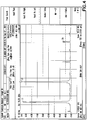
- FIG. 1 is a spectral plot of amplitude as a function of frequency using conventional intermodulation correction techniques.
- a first carrier 10 is present at a first frequency and has an amplitude of approximately 16 dBm.
- a second carrier 20 is present at a second frequency and also has an amplitude of approximately 16 dBm.
- a fifth-order intermodulation component 30 that is 45.2 MHz below the second carrier 20 has an amplitude that is only 67.848 dB below the amplitudes of the first and second carriers 10, 20. Accordingly, the spectral plot of FIG. 1 clearly indicates that at least one intermodulation product (i.e., intermodulation component 30) is not within the allowable limits set forth in the 3GPP specification.
- FIG. 1 The plot of FIG. 1 was prepared using the conventional approach of determining an integer delay for DPD. However, this plot reveals that determining an integer delay for DPD is not accurate enough to achieve correction of intermodulation products in the 1800-MHz band. Although this example is specific to the 1800MHz band, similar considerations apply to other bands which have a relatively wide bandwidth occupancy.
- FIG. 1 demonstrates failure of the fifth intermodulation product (IM5), it may be noted that third intermodulation product (IM3) failures were observed in the context of somewhat larger signal separations as well as somewhat smaller signal separations, such as 25MHz, for example. As described in greater detail hereinafter, the failure of these intermodulation products is a direct result of not incorporating a fractional delay into an intermodulation compensation scheme.
- One possible solution for ensuring that intermodulation products do not exceed the standards set forth in the 3GPP specification is to mask the problem. For example, one could conceive a solution by splitting the 1800-MHz band into two or three overlapping bands. Such an approach would help attenuate the distant IM5 and IM7 products as they will be out of band at the front end duplex filter. However, this means providing either two or three different product variants, or including two different transmit filters in a single product. A better solution is needed.
- a fractional delay is determined, estimated, or computed.
- the fractional delay is used computation as part of the delay computation, thus avoiding rounding to the nearest integer. For example, computing the correct delay of 154.7 is better for distant intermodulation products than rounding the delay off to 155.
- FIG. 2 is a logical flow diagram that illustrates the operation of an example set of methods, and a result of execution of computer program instructions embodied on a computer readable memory, in accordance with various example embodiments.
- the various blocks shown in FIG. 2 may be viewed as method steps, and/or as operations that result from operation of computer program code, and/or as a plurality of coupled logic circuit elements constructed to carry out the associated functions.
- T1 a coarse time delay represented by an integer T1
- T1 a coarse time delay represented by an integer T1
- T1 a coarse time delay represented by an integer T1
- T1 a coarse time delay represented by an integer T1
- T1 a coarse time delay represented by an integer T1
- T1
- the operational sequence of FIG. 2 progresses to block 205 where the transmitted signal waveform is shifted by a set of offsets comprising a plurality of non-integer fractional steps from (T1 - Xd) to (T1 + Xd) where T1 is the integer and S1 is a non-integer fractional step size value for defining the plurality of non-integer fractional steps about the integer T1 up to a limit Xd such that the non-integer fractional steps progress in a positive direction as well as a negative direction from the integer T1.
- a field-programmable gate array (FPGA) implementation may implement fractional delay by inserting additional gates between a transmit path and a feedback path. Normally, each of the gate arrays of the FPGA would be configured to provide a constant or fixed delay.
- the operational sequence of FIG. 2 progresses to block 207 where, at each of the plurality of non-integer fractional steps, the transmitted signal waveform is correlated with a feedback signal waveform.
- a correct or accurate value for the fractional delay is obtained by selecting a fractional step of the plurality of non-integer fractional steps that provides a highest, greatest, or maximum correlation of the transmitted signal waveform to the feedback signal waveform.
- the correct or accurate value of the fractional delay is applied to the transmitted signal waveform to provide a compensated transmitted signal waveform.
- the compensated transmitted signal waveform is combined with the feedback signal waveform to reduce or eliminate at least one intermodulation component of the RF power amplifier.
- the transmitted signal waveform of blocks 201, 203, 205, 207 and 209 represents either a pre-distorted waveform for correcting RF power amplifier linearity, or a non pre-distorted waveform to which a correction may subsequently be applied. Once the correct value of fractional delay is obtained, this value is kept fixed for a certain or predetermined period of time. Using the correct fractional delay results in improved intermodulation correction for the RF power amplifier.
- blocks 203, 205, 207 and 209 are repeated in response to aging, temperature fluctuations, changes in RF power amplifier supply voltage, changes in RF power amplifier current consumption, or measuring an incorrect fractional delay as evidenced by degraded intermodulation performance.
- the operational sequence of FIG. 2 further enhances correlation accuracy by considering higher-order products in the transmitted signal waveform.
- the transmitted signal waveform is x(t)
- the accuracy of the correlation can be improved by including higher-order terms for the transmitted waveform to improve correlation accuracy, thereby resulting in a more accurate estimate of fractional delay.
- the shifted transmitted signal waveform of block 205 may be passed through an actual RF power amplifier model. The resultant transmitted signal waveform y(t) is then used to correlate with the feedback signal waveform.
- the consideration of higher-order products into the transmitted signal waveform implements a simplified RF power amplifier model that utilizes only third-order intermodulation products.
- actual implementations may be configured to consider intermodulation products in addition to, or in lieu of, the third-order intermodulation products.
- Considering third-order intermodulation products as well as higher-order intermodulation products will enhance the correlation between the transmitted signal waveform and the feedback signal waveform relative to considering third-order intermodulation products only.
- the approach of passing the shifted transmitted signal waveform through an actual RF power amplifier model may produce better correlation accuracy than simply considering higher-order products in the transmitted signal waveform.
- FIG. 3 is a block diagram of an illustrative apparatus in which the example embodiments of FIG. 2 may be practiced.
- a digital input signal 301 is provided, for example, in quadrature form including an I component and a Q component.
- the digital input signal 301 is received by a digital predistorter (DPD) 309.
- the DPD 309 may, but need not, be implemented using a field-programmable gate array (FPGA) 303.
- the output of the DPD 309 including a first predistored output signal 341 corresponding to the I component and a second predistorted output signal 345 corresponding to the Q component, is received by a quadrature modulation compensator (QMC) 313.
- QMC quadrature modulation compensator
- the QMC 313 provides a first compensated and predistorted output signal corresponding to the I component to a first digital to analog converter (DAC) 317.
- the QMC 313 also provides a second compensated and predistorted output signal corresponding to the Q component to a second digital to analog converter (DAC) 319.
- the first predistored output signal 341 corresponding to the I component and the second predistorted output signal 345 corresponding to the Q component are each processed by a delay 347 line.
- the delayed first and second predistored output signals 341 and 345 are received by a correction algorithm 307.
- the correction algorithm 307 also receives a delayed digital input signal 301 that has been delayed by a delay 349 line.
- the correction algorithm includes computer-executable instructions for performing the operational sequence of FIG. 2 .
- the correction algorithm 307 may, but need not, be executed using a digital signal processor (DSP) 305.
- the DSP 305 may include a computer or data processor 351 operatively coupled to a tangible computer-readable memory 353 wherein the memory 353 stores instructions for implementing the correction algorithm 307 as previously described in connection with the operational sequence of FIG. 2 .
- the output of DAC 317 is filtered by a first lowpass filter 323, and the filtered output is received by a modulator (MOD) 327.
- the output of DAC 319 is filtered by a second lowpass filter 325, and the filtered output is received by the MOD 327.
- the MOD 327 also receives an RF carrier signal generated by a local oscillator (LO) 329.
- the MOD 327 applies a modulating signal comprising the filtered outputs of the DACs 317 and 319 to the RF carrier signal generated by the LO 329 to provide a modulated signal that is received by an input of an RF power amplifier (PA) 335.
- PA RF power amplifier
- the LO 329 may, but need not, generate an RF carrier signal at a desired or specified RF output 355 frequency.
- the LO 329 may generate a signal at a lower frequency than the desired or specified RF output 355 frequency, in which case the MOD 327 may include a frequency up-converter for converting the lower frequency to the desired or specified RF output 355 frequency.
- a portion of the RF output 355 of the PA 335 is sampled 337 and filtered by a bandpass filter 333.
- the filtered sampled signal is received by an analog to digital converter (ADC) 321 which converts the filtered sampled signal into a digitized sampled signal.
- ADC analog to digital converter
- DDC digital downconverter
- the data processor 351 and the memory 353 are described as being provided in the form of the DSP 305 for illustrative purposes only. It should be noted that the memory 353 and the data processor 351 may each be implemented using discrete elements. Alternatively, the memory 353 and the data processor 351 could be integrated into a single application-specific integrated circuit chip. More generally, various example embodiments may be implemented by hardware, or by a combination of software and hardware (and firmware).
- the memory 353 may be of any type suitable to the local technical environment and may be implemented using any suitable data storage technology, such as semiconductor based memory devices, flash memory, magnetic memory devices and systems, optical memory devices and systems, fixed memory and removable memory.
- the data processor 351 may be of any type suitable to the local technical environment, and may include one or more of general purpose computers, special purpose computers, microprocessors, digital signal processors (DSPs) and processors based on a multicore processor architecture, as non-limiting examples.
- general purpose computers special purpose computers
- microprocessors microprocessors
- DSPs digital signal processors
- processors based on a multicore processor architecture, as non-limiting examples.
- FIG. 4 is a spectral plot of amplitude as a function of frequency using any of the intermodulation correction methods described in conjunction with FIG. 2 .
- a first carrier 11 is present at a first frequency and has an amplitude of approximately 16 dBm.
- a second carrier 21 is present at a second frequency that is 22.6 MHz above the first frequency.
- the second carrier 21 also has an amplitude of approximately 16 dBm.
- a fifth-order intermodulation component 31 that is 45.2 MHz above the second carrier 21 has an amplitude that is 75.9 dB below the amplitudes of the first and second carriers 11, 21. Accordingly, the spectral plot of FIG. 4 clearly indicates that all intermodulation products are within the allowable limits set forth in the 3GPP specification.
- the preferred embodiments of the invention described herein provide various technical effects and benefits which include, but are not limited to, reducing or eliminating intermodulation components in an RF power amplifier.
- An additional effect is the avoidance of having to provide multiple product variants for the same frequency band.
- a single filter may be employed, thereby saving unit space and cost.
- the various example embodiments may be implemented in hardware or special purpose circuits, software, logic or any combination thereof
- some aspects may be implemented in hardware, while other aspects may be implemented in firmware or software which may be executed by a controller, microprocessor or other computing device, although not limited thereto.
- firmware or software which may be executed by a controller, microprocessor or other computing device, although not limited thereto. While various aspects of the example embodiments may be illustrated and described as block diagrams, flow charts, or using some other pictorial representation, it is well understood that these blocks, apparatus, systems, techniques or methods described herein may be implemented in, as nonlimiting examples, hardware, software, firmware, special purpose circuits or logic, general purpose hardware or controller or other computing devices, or some combination thereof.
- the integrated circuit, or circuits may comprise circuitry (as well as possibly firmware) for embodying at least one or more of a data processor or data processors, a digital signal processor or processors, baseband circuitry and radio frequency circuitry that are configurable so as to operate in accordance with the example embodiments.
- example embodiments have been described above, it should be appreciated that the example embodiments are not limited for use with only one particular type of wireless communication system, and that they may be used to advantage in other wireless communication systems such as for example E-UTRAN (UTRAN-LTE), WLAN, UTRAN, or GSM, as appropriate.
- E-UTRAN UTRAN-LTE
- WLAN Wireless Fidelity
- UTRAN Wireless Fidelity
- GSM Global System for Mobile communications
- connection means any connection or coupling, either direct or indirect, between two or more elements, and may encompass the presence of one or more intermediate elements between two elements that are “connected” or “coupled” together.
- the coupling or connection between the elements can be physical, logical, or a combination thereof.
- two elements may be considered to be “connected” or “coupled” together by the use of one or more wires, cables and/or printed electrical connections, as well as by the use of electromagnetic energy, such as electromagnetic energy having wavelengths in the radio frequency region, the microwave region and the optical (both visible and invisible) region, as several non-limiting and non-exhaustive examples.
- An example embodiment provides a method for selectively performing beam formation using a RF chip-based antenna array.
- the method includes determining (such as by a processor for example) whether to use a plurality of antenna arrays in one or more common carrier substrates in either a single group or a plurality of groups.
- the method also includes, in response to determining to use the plurality of antenna arrays in a single group, providing (such as by a transmitter for example) a single coupling factor to all antenna arrays in the plurality of antenna arrays and, in response to determining to use the plurality of antenna arrays in a plurality of groups, providing (such as by a transmitter for example), for each group in the plurality of groups, a group-specific coupling factor to each antenna array in the group.
- the apparatus includes at least one processor (such as DP 1224 for example) and at least one memory (such as MEM 1226 for example) storing computer program code (such as PROG 1228 for example).
- the at least one memory and the computer program code are configured to, with the at least one processor, cause the apparatus to perform actions.
- the actions include determining whether to use a plurality of antenna arrays in one or more common carrier substrates in either a single group or a plurality of groups.
- the actions also include, in response to determining to use the plurality of antenna arrays in a single group, providing a single coupling factor to all antenna arrays in the plurality of antenna arrays and, in response to determining to use the plurality of antenna arrays in a plurality of groups, providing, for each group in the plurality of groups, a group-specific coupling factor to each antenna array in the group.
- Another example embodiment provides a computer readable medium for selectively performing beam formation using a RF chip-based antenna array.
- the computer readable medium (such as MEM 1226 for example) is tangibly encoded with a computer program (such as PROG 1228 for example) executable by a processor (such as DP 1224 for example) to perform actions.
- the actions include determining whether to use a plurality of antenna arrays in one or more common carrier substrates in either a single group or a plurality of groups.
- the actions also include, in response to determining to use the plurality of antenna arrays in a single group, providing a single coupling factor to all antenna arrays in the plurality of antenna arrays and, in response to determining to use the plurality of antenna arrays in a plurality of groups, providing, for each group in the plurality of groups, a group-specific coupling factor to each antenna array in the group.
- the apparatus includes means for determining (such as a processor for example) whether to use a plurality of antenna arrays in one or more common carrier substrates in either a single group or a plurality of groups.
- the apparatus also includes means for providing (such as a transmitter for example) a single coupling factor to all antenna arrays in the plurality of antenna arrays in response to determining to use the plurality of antenna arrays in a single group, and means for providing (such as a transmitter for example), for each group in the plurality of groups, a group-specific coupling factor to each antenna array in the group in response to determining to use the plurality of antenna arrays in a plurality of groups.
- the inventors have discovered that the integer delay may not be sufficient to correct wide band 2C-GSM (or 2C-8PSK) or even 6C-GSM (or 6C-8PSK) waveforms.
- a correlation of Transmit (Tx) and Feedback (Fb) will provide a delay value up to the closest integer.
- the integer here refers to a single Tx sample. For example 307.2Msps will provide integer samples spaced at 3.25ns spacing.
- 2C and 6C waveforms are discussed herein, some embodiments are not limited to those. Some embodiments of the invention can be applied, for example, to 3, 4, 5 carrier wideband GSM as well as wideband WCDMA and LTE waveforms.
- fractional samples are used to achieve the proper correction of IM3 (3 rd order intermodulation products) and IM5 (5 th order intermodulation products) provided these products are within the RF band filter (e.g., cavity filter).
- fractional delay model may be also limited by the hardware and software configuration (for example, the hardware and available ASIC (Application Specific Integrated Circuit) flexibility).
- the other factors that may limit the use of the fractional delay include, for examples, the convergence speed, refinement of the fractional delay value, and continuous tracking of the fractional delay value for correctness over time, typically for months and years.
- Convergence speed and refinement may be used at the beginning of carrier initiation for faster convergence towards the proper fractional delay. Faster convergence may ensure less emission violations during the reconfiguration of the carriers. The reconfiguration of carriers may cause the recalculation of the fractional delay value.
- continuous and long term tracking of the delay may be used, for example, for avoiding changes due to hardware aging.
- Hardware aging can also add small changes to the total delay (e.g. fractional changes). These may need to be tracked over longer durations, for example, to avoid emission violations caused by the drift of delay value.
- fractional delay options can be categorized, for example, according to their accuracy and their suitability to available ASIC options.
- an optimum fractional delay algorithm is provided depending on hardware (HW), software (SW) and/or time considerations.
- HW hardware
- SW software
- Some embodiments optimize the use of fractional delay computations to improve intermodulation performance, for example, to enable appropriate convergence speed and accuracy without having to make unnecessary accommodations in new and installed systems.
- the inventors have studied various algorithms based on convergence speed and accuracy of the fractional delay model.
- a single model may not be able to satisfy the needs for convergence speed, refinement of accuracy, and long term tacking due to, for example, hardware aging.
- larger and smaller scale (e.g., a small cell BTS) BTSs have different hardware and software configuration limitations that affect the use of the fractional delay for improving the performance of an RF power amplifier.
- different hardware configurations may include ASIC(s) having varying capabilities.
- the optimum solution for start up (for example, carrier configuration) of a given hardware and software configuration is a sub-optimum for long term use (for example, tacking of fractional delay and correcting for drift).
- Figure 5 is a flowchart showing an algorithm for performing the method according to some embodiments of the invention.
- a fractional delay solution is determined for a hardware and software configuration dependent on a selected criteria selected from predetermined criteria (501).
- the fractional delay solution may be applied, for example, during the carrier configuration.
- the predetermined criteria include, for example, a convergence speed for calculating a fractional delay, an accuracy requirement of the fractional delay, and a tracking requirement for correctness over time of the fractional delay.
- a fractional delay value is calculated (502).
- the fractional delay value is determined by correlating the transmitted signal waveform with the feedback signal waveform.
- the fractional delay value is used to eliminate at least one intermodulation product of an RF power amplifier (503).
- the fractional delay solution provides the fractional delay value that can be rapidly calculated for the hardware and software configuration.
- the rapidly calculated fractional delay value may not be optimized for accuracy.
- around 35dB of correction may be the desired long term correction.
- the fractional delay value may provide a very rapidly achieved solution, but it may only provide a correction of, for example, around 30 or 32 dB. Accordingly, for example, after a period of time from the carrier configuration has elapsed and/or for long term tracking, there may be a need for refinement of the fractional delay value used to eliminate the intermodulation production product of an RF power amplifier to achieve the desired correction.
- a need for a subsequent fractional delay solution is thus determined (504).
- the determination is, for example, based on at least one of factors: a time duration from the carrier configuration, a desired accuracy of the fractional delay value, and an expected or measured aging of hardware elements of the hardware and software configuration.
- a subsequent fractional delay solution is determined for the hardware and software configuration dependent on another selected criteria selected from the at least one predetermined criteria (505).
- the subsequent fractional delay solution may be applied, for example, during a time subsequent to the carrier configuration.
- a subsequent fractional delay value is determined by correlating the subsequent transmitted signal waveform with the subsequent feedback signal waveform (506).
- the subsequent fractional delay value is used to continue to eliminate at least one intermodulation product of an RF power amplifier (507).
- the application of the fractional delay solution may provide a better MSE (Mean Square Error) as compared with not applying any fractional delay, for example.
- MSE Mel Square Error
- the fractional delay solution can result in a MSE metric of MSE_i.
- the hardware and software configuration can then take the time necessary to compute a more accurate correction using the subsequent fractional delay solution.
- the switch from the use of the fractional delay solution to the subsequent fractional delay solution may be dependent on the hardware and software configuration. For example, it may depend on the complexity of the RF power amplifier.
- around 30 second minimum time may be applied before the switch over from the less accurate, faster-to-calculate fractional delay solution to the more accurate, slower-to-calculate subsequent fractional delay solution.
- the subsequent fractional delay solution can result in a MSE metric of MSE_f.
- the application of the subsequent fractional delay method improves the DPD correction, for example, from around 32dB to around 35dB.
- the determination of when to switch to the use of the subsequent fractional delay solution may be based, for example, on at least one of a measurement of the MSE, available processing power of the hardware and software configuration, and the requirement for accuracy. For example, a small base station may require less accuracy due to the relative simplicity of the hardware and software configuration as compared to a larger base station.
- FIG. 6 is a flowchart showing an algorithm for performing 502 of FIG. 5 for determining a fractional delay value from the correlation of a corresponding sample of a transmitted signal waveform and a respective sample of a feedback signal waveform according to some embodiments of the invention.
- a sample Tx1 of the transmitted signal waveform is obtained 502(a)
- a sample Fb1 of the feedback signal waveform is obtained 502(b).
- Tx1 and Fb1 are correlated 502(c).
- TxN samples of the transmitted signal are obtained 502(aN), along with FbN samples of the feedback signal 502(bN), and the TxN samples are correlated with the FbN samples 502(cN).
- the fractional delay value is determined from the correlation of the TxN samples with the FbN samples 502(d).
- FIG. 7 is a flowchart showing an algorithm for performing 506 of FIG. 5 for determining a subsequent fractional delay value from the correlation of a corresponding sample of a subsequent transmitted signal waveform and a respective sample of a subsequent feedback signal waveform according to some embodiments of the invention.
- a sample Tx1 of the subsequent transmitted signal waveform is obtained 506(a)
- a sample Fb1 of the subsequent feedback signal waveform is obtained 506(b).
- Tx1 and Fb1 are then correlated 506(c).
- TxN samples of the subsequent transmitted signal are obtained 506(aN), along with FbN samples of the subsequent feedback signal 506(bN), and the TxN samples are correlated with the FbN samples 506(cN).
- the subsequent fractional delay value is determined from the correlation of the TxN samples with the FbN samples 506(d).
- a sample of the transmitted waveform is correlated with a sample of the feedback waveform.
- the fractional delay solution may include a transmitted signal waveform and a feedback signal waveform.
- the fractional delay value is determined by correlating respective samples of the transmitted signal waveform with corresponding samples of the feedback signal.
- the subsequent fractional delay solution may include a subsequent transmitted signal waveform and a subsequent feedback signal waveform.
- the subsequent fractional delay value is determined by correlating respective samples of the subsequent transmitted signal waveform with corresponding samples of the subsequent feedback signal waveform.
- FIG. 8 is a flowchart showing an alternative algorithm for performing 502 of FIG. 5 for determining a fractional delay from the correlation of samples of the transmitted signal waveform each with a same sample of the feedback signal waveform according to some embodiments of the invention.
- Tx1 through TxN samples of the transmitted signal waveform are obtained 502(a), and a sample Fb1 of the feedback signal waveform is obtained 502(b).
- the samples of the transmitted signal waveform Tx1 through TxN are each with a same sample of the feedback signal waveform 502(c).
- the fractional delay value fractional delay is determined from the correlation of samples of the transmitted signal waveform Tx1 through TxN each with a same sample Fb1 of the feedback signal waveform 502(d).
- FIG. 9 is a flowchart showing an alternative algorithm for performing 506 of FIG. 5 for determining a subsequent fractional delay from the correlation of samples of the subsequent transmitted signal waveform each with a same sample of the subsequent feedback signal waveform according to some embodiments of the invention.
- Tx1 through TxN samples of the subsequent transmitted signal waveform are obtained 506(a), and a sample Fb1 of the subsequent feedback signal waveform is obtained 506(b).
- the samples of the subsequent transmitted signal waveform Tx1 through TxN are each with a same sample of the subsequent feedback signal waveform 506(c).
- the subsequent fractional delay value subsequent fractional delay is determined from the correlation of samples of the subsequent transmitted signal waveform Tx1 through TxN each with a same sample Fb1 of the subsequent feedback signal waveform 506(d).
- fewer feedback samples than the transmitted signal samples are needed. For example, as show FIG.9 , only a single feedback waveform sample is needed.
- the correlation consists of (Tx1,Fb1), (Tx2,Fb1), (Tx3, Fb1) across (Tx10,Fb1).
- Tx1....Tx10 are fractional delay steps and Fb1 is a single capture of feedback data.
- fewer feedback samples than the transmitted signal samples are collected.
- a single transmitted signal sample and a single feedback signal sample are collected, and the fractional delay value is determined by correlating the single transmitted signal sample and the single feedback signal sample.
- the single transmitted signal may be shifted by fractions of a sample via a filter, and the shifted Tx signals may be not transmitted, but rather used for correlations purposes only.
- the fractional delay solution includes a transmitted signal waveform and a feedback signal waveform, and the fractional delay value is determined by correlating samples of the fractional delay solution each with a same sample of the feedback signal waveform.
- the subsequent fractional delay solution includes a subsequent transmitted signal waveform and a subsequent feedback signal waveform, and the subsequent fractional delay value is determined by correlating samples of the subsequent fractional delay solution each with a same sample of the subsequent feedback signal waveform.
- the fractional delay value may be determined by correlating samples of the transmitted waveform each with a same sample of the feedback signal waveform, and the subsequent fractional delay value is determined by correlating a same sample of the subsequent transmitted signal waveform with samples of the subsequent feedback signal waveform.
- the fractional delay value is computed, for example, with (Tx1, Fb1), (Tx2, Fb1)...(Txn, Fb1); and the subsequent fractional delay value is computed with (Txp, Fbp), (Txp, Fb(p+1))... (Txp, Fb(p+n). That is, the same sample of the subsequent transmitted signal waveform (Txp) is correlated with samples of the subsequent feedback signal waveform (Fbp, Fb(p+1)...Fb(p+n)).
- the corresponding and subsequent fractional delay value may be applied to the respective and subsequent transmitted signal waveform to provide a respective and subsequent compensated transmitted signal waveform.
- the respective and subsequent compensated transmitted signal waveform may be combined with the respective and subsequent feedback signal waveform to eliminate the least one intermodulation product of the RF power amplifier.
- the fractional delay improves, for example, the intermodulation correction, and this improvement can be detected through the MSE value. The higher the accuracy, the better the corrected intermodulation product of the RF power amplifier.
- the predetermined criteria comprises at least one of a convergence speed for calculating the fractional delay, an accuracy requirement of the fractional delay, and a tracking requirement for correcting for drift over time of the fractional delay. Since accurate computation of the fractional delay value may take time, a coarse but fast estimate may be obtained first using the fractional delay solution before a slower but more accurate computation is performed using the subsequent fractional delay solution improving the fractional delay accuracy.
- the selected criteria used for determining the fractional delay solution and the selected criteria used for determining the subsequent fractional delay solution could be the same criteria, for example, convergence speed, where the determination of the solution depends on a desired time allowed for the calculation of the fractional delay value.
- the desired time for the calculation of an initial fractional delay value will be relatively shorter (because time to achieve the configuration is important) than the desired time for the calculation of the subsequent fractional delay value (because accuracy of the delay value over a longer period of time is important).
- the desired time for the calculation may be a determining criteria for the calculation of the initial fractional delay value, while the accuracy may be a determining criteria for the calculation of the subsequent fractional delay value.
- the fractional delay solution calculates the fractional delay with faster convergence speed, but less accuracy, than the subsequent fractional delay solution calculates the fractional delay value.
- the subsequent fractional delay solution may take more time, for example, to perform relatively more complex calculations to obtained the improve accuracy of the subsequent fractional delay value.
- the subsequent fractional delay solution calculates the subsequently used fractional delay value with greater accuracy than the initially used fractional delay that is calculated by the fractional delay solution.
- the subsequent fractional delay solution calculates the subsequently used fractional delay with greater tracking accuracy than the initially used fractional delay calculated by the fractional delay solution. The result is better tracking to correct for drift of the correct fractional delay value for a desired accuracy over time.
- the need for the subsequent fractional delay solution may be determined based on a predetermined length of time elapsing from the determination of the fractional delay solution and/or a predetermined length of time elapsing since the configuration.
- the need for the subsequent fraction delay solution may be determined based on aging of hardware elements of the hardware and software configuration and/or temperature fluctuations.
- the fractional delay solution may be based on Mean Square Error differences between the transmitted signal waveform and the feedback signal waveform. When the fractional delay drifts due to, for example, aging of the hardware elements and/or temperature change, the correction of the intermodulation product of the RF power amplifier may degrade.
- the Mean Square Error differences between the transmitted signal waveform and the feedback signal waveform may also change as the fractional delay value drifts, making the MSE a useful mechanism for tracking the fractional delay value and determining the need for the subsequent fractional delay solution.
- the subsequent fractional delay solution is used to compensate for the limitations of a radio system's hardware and software configuration. For example, sub-optimum methods (with regards to accuracy) that are very fast (with regards to calculation speed) can be used first as a fractional delay solution. Then, resources of the hardware and software configuration are given much longer calculation time to obtain the desired accuracy using the subsequent fractional delay solution.
- the fractional delay mechanism is an essential mechanism that provides the Digital Pre-Distortion (DPD) algorithm with the correct delay value.
- the DPD algorithm Given the correct fractional delay value, the DPD algorithm is able to correct the intermodulation products that are within the band filter (cavity filter).
- a determination of the need for the subsequent fractional delay solution can be based on the distance of the intermodulation products from an actual carrier signal generated by the RF power amplifier. Alternatively, or additionally, the determination of the need for the subsequent fractional delay solution can be based on a bandwidth of communication signals generated by the RF power amplifier.
- option A) being the longest to calculate and the most accurate
- E) being the shortest to calculate and least accurate.
- the calculation speed is determined, for example, according to the number of operations that have to be performed for a given fractional delay solution.
- the accuracy of options B), C), and D are of descending order.
- the discussion herein lists the options in terms of Tx signal variations and Feedback signal, where the fractional delay is determined based on correlating Tx variations listed with the Feedback signal.
- Option A As compared to the other options listed, this turns out to be a relatively more accurate error model based on Mean Square Error differences of Tx and Feedback (Fb) signals.
- the Feedback signal (FB) is corrected (Digital pre-distortion is turned ON).
- Option A is a good solution for long term tracking.
- Option B Similar to option A, but not including the Nth order IM products in the Tx signal. Tx is still un-predistorted. Fb is still corrected (e.g., good for smaller ASICs). This option is faster as compared with option A.
- Tx signal is pre-distorted.
- the Feedback signal is still corrected. This is a good solution for the higher convergence speed that is needed at start up. Although less accurate, this option can use as a stating point to refine the fractional delay value on an ongoing basis.
- the Feedback signal is not corrected. This means that correlation is based on un-corrected IM products.
- Option E This option consists of a pre-distorted Tx, with no higher order IM products included in the Tx. Fb signal is corrected. This option is the fastest method (compared to options A - D) to obtain a quick estimate. Other methods (options) for the fractional delay solution can use the delay value obtained using Option E as a starting point.
- Option E) obtains an estimate of the fractional delay value quickly, and can be used initially to rapidly obtain a good delay estimation.
- options C), B) or A) can be used for long term tacking with increased accuracy.
- the selection of which option C), B) or A) to use can be dependent on the hardware and software configuration.
- Option D An alternative option is similar to Option D).
- the feedback signal is not corrected, and the Tx is undistorted but does not contain Nth order products.
- the transmitted signal waveform may be an un-predistorted signal including N th order intermodulation products and the feedback signal waveform may be a predistorted signal; or, the transmitted signal waveform may be an un-predistorted signal not including N th order intermodulation products and the feedback signal waveform is a predistorted signal; or, the transmitted signal waveform may be a predistorted signal including N th order intermodulation products and the feedback signal waveform is a predistorted signal; or, the transmitted signal waveform may be an un-predistorted signal including N th order intermodulation products and the feedback signal waveform is an uncorrected signal; or, the transmitted signal waveform may be a predistorted signal not including N th order intermodulation products and the feedback signal waveform is a predistorted signal; and the subsequent transmitted signal waveform may be an un-predistorted signal including N th order intermodulation products and the subsequent feedback signal waveform is a predistorted signal; or, the subsequent transmitted signal waveform may be an un-predistorted signal not including N th order intermodulation products and the subsequent feedback signal
- options D) or C) can be used along with an intermittent use of option A) to check and refine the fractional delay value used to improve the performance of the RF power amplifier.
- option D) is the simplest to calculate and option A) is the most complex to calculate. Generally, the simpler to calculate option is used when speed is desired (such as at the initial configuration) and more complex to calculate options are used when accuracy is desired (such as to correct for hardware aging and/or temperature fluctuations over time).
- some embodiments of the invention may improve intermodulation performance include avoiding multiple product variants for the same band, saving cost in terms of R&D, testing, logistics, and bookkeeping; avoiding having to use two transmit front end filters per unit saving unit space and cost; and providing multiple options where by the optimum solution is based on hardware and software configuration limitations as well as short and long term criteria.
- FIG. 10 is a functional block diagram illustrating a structure for an apparatus comprising means to perform a method according to some embodiments of the invention.
- the structure comprises one or more (micro)processors and other hardware and software elements configured for radio frequency communication.
- the structure may be incorporated, for example, in a base station, micro-base station, mobile terminal and other hardware and software configurations used in a radio communication system.
- the structure includes means for determining a fractional delay solution 410 for the hardware and software configuration dependent on a selected criteria selected from at least one predetermined criteria.
- Means for calculating a fractional delay value 412 using the fractional delay solution are provided.
- Means for eliminating at least one intermodulation product 414 of an RF power amplifier using the fractional delay value are provided.
- Means for determining a need for a subsequent fractional delay solution 416 may also be provided.
- Means for determining the subsequent fractional delay solution 418 may also be provided.
- Means for calculating a subsequent fracational delay solution 420 may also be provided to calculated a subsequent fractional delay value for the hardware and software configuration dependent on another selected criteria selected from the at least one predetermined criteria.
- the means to eliminate the at least one intermodulation product 414 of the RF power amplifier may use the subsequent fractional delay value to continue to eliminate the at least one intermodulation product of the RF power amplifier.
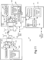
- FIG. 11 shows a block diagram of an example system in which the example embodiments may be practiced.
- a UE 110 is in wireless communication with a wireless network 100.
- the user equipment 110 includes one or more processors 120, one or more memories 125, and one or more transceivers 130 interconnected through one or more buses 127.
- Each of the one or more transceivers 130 includes a receiver, Rx, 132 and a transmitter, Tx, 133.
- the one or more buses 127 may be address, data, or control buses, and may include any interconnection mechanism, such as a series of lines on a motherboard or integrated circuit, fiber optics or other optical communication equipment, and the like.
- the one or more transceivers 130 are connected to one or more antennas 128.
- the one or more memories 125 include computer program code 123.
- the UE 110 communicates with eNB 170 via a wireless link 111.
- the eNB 170 is a base station that provides access by wireless devices such as the UE 110 to the wireless network 100.
- the eNB 170 includes one or more processors 152, one or more memories 155, one or more network interfaces (N/W I/F(s)) 161, and one or more transceivers 160 interconnected through one or more buses 157.
- Each of the one or more transceivers 160 includes a receiver, Rx, 162 and a transmitter, Tx, 163.
- the one or more transceivers 160 are connected to one or more antennas 158.
- the one or more memories 155 include computer program code 153.
- the eNB 170 includes a delay module 150, comprising one of or both parts 150-1 and/or 150-2, which may be implemented in a number of ways.
- the delay module 150 may be implemented in hardware as delay module 150-1, such as being implemented as part of the one or more processors 152.
- the delay module 150-1 may be implemented also as an integrated circuit or through other hardware such as a programmable gate array.
- the delay module 150 may be implemented as delay module 150-2, which is implemented as computer program code 153 and is executed by the one or more processors 152.
- the one or more memories 155 and the computer program code 153 are configured to, with the one or more processors 152, cause the eNB 170 to perform one or more of the operations as described herein.
- the one or more network interfaces 161 communicate over a network such as via the links 176 and 131.
- Two or more eNBs 170 communicate using, e.g., link 176.
- the link 176 may be wired or wireless or both and may implement, e.g., an X2 interface.
- the one or more buses 157 may be address, data, or control buses, and may include any interconnection mechanism, such as a series of lines on a motherboard or integrated circuit, fiber optics or other optical communication equipment, wireless channels, and the like.
- the one or more transceivers 160 may be implemented as a remote radio head (RRH) 195, with the other elements of the eNB 170 being physically in a different location from the RRH, and the one or more buses 157 could be implemented in part as fiber optic cable to connect the other elements of the eNB 170 to the RRH 195.
- RRH remote radio head
- the wireless network 100 may include a network control element (NCE) 190 that may include MME/SGW functionality, and which provides connectivity with a further network, such as a telephone network and/or a data communications network (e.g., the Internet).
- the eNB 170 is coupled via a link 131 to the NCE 190.
- the link 131 may be implemented as, e.g., an S1 interface.
- the NCE 190 includes one or more processors 175, one or more memories 171, and one or more network interfaces (N/W I/F(s)) 180, interconnected through one or more buses 185.
- the one or more memories 171 include computer program code 173.
- the one or more memories 171 and the computer program code 173 are configured to, with the one or more processors 175, cause the NCE 190 to perform one or more operations.
- the wireless network 100 may implement network virtualization, which is the process of combining hardware and software network resources and network functionality into a single, software-based administrative entity, a virtual network.
- Network virtualization involves platform virtualization, often combined with resource virtualization.
- Network virtualization is categorized as either external, combining many networks, or parts of networks, into a virtual unit, or internal, providing network-like functionality to software containers on a single system. Note that the virtualized entities that result from the network virtualization are still implemented using hardware such as processors 152 or 175 and memories 155 and 171.
- the computer readable memories 125, 155, and 171 may be of any type suitable to the local technical environment and may be implemented using any suitable data storage technology, such as semiconductor based memory devices, flash memory, magnetic memory devices and systems, optical memory devices and systems, fixed memory and removable memory.
- the processors 120, 152, and 175 may be of any type suitable to the local technical environment, and may include one or more of general purpose computers, special purpose computers, microprocessors, digital signal processors (DSPs) and processors based on a multi-core processor architecture, as non-limiting examples.
- the various embodiments of the user equipment 110 can include, but are not limited to, cellular telephones such as smart phones, personal digital assistants (PDAs) having wireless communication capabilities, portable computers having wireless communication capabilities, image capture devices such as digital cameras having wireless communication capabilities, gaming devices having wireless communication capabilities, music storage and playback appliances having wireless communication capabilities, Internet appliances permitting wireless Internet access and browsing, tablets with wireless communication capabilities, as well as portable units or terminals that incorporate combinations of such functions.
- PDAs personal digital assistants
- portable computers having wireless communication capabilities
- image capture devices such as digital cameras having wireless communication capabilities
- gaming devices having wireless communication capabilities
- music storage and playback appliances having wireless communication capabilities
- Internet appliances permitting wireless Internet access and browsing, tablets with wireless communication capabilities, as well as portable units or terminals that incorporate combinations of such functions.
- Embodiments herein may be implemented in software (executed by one or more processors), hardware (e.g., an application specific integrated circuit), or a combination of software and hardware.
- the software e.g., application logic, an instruction set
- a "computer-readable medium” may be any media or means that can contain, store, communicate, propagate or transport the instructions for use by or in connection with an instruction execution system, apparatus, or device, such as a computer, with one example of a computer described and depicted, e.g., in FIG. 11 .
- a computer-readable medium may comprise a computer-readable storage medium (e.g., memories 125, 155, 171 or other device) that may be any media or means that can contain or store the instructions for use by or in connection with an instruction execution system, apparatus, or device, such as a computer.
- a computer-readable storage medium e.g., memories 125, 155, 171 or other device
- the different functions discussed herein may be performed in a different order and/or concurrently with each other. Furthermore, if desired, one or more of the above-described functions may be optional or may be combined.
Landscapes
- Engineering & Computer Science (AREA)
- Power Engineering (AREA)
- Microelectronics & Electronic Packaging (AREA)
- Physics & Mathematics (AREA)
- Nonlinear Science (AREA)
- Computer Networks & Wireless Communication (AREA)
- Signal Processing (AREA)
- Amplifiers (AREA)
- Transmitters (AREA)
Claims (13)
- Un procédé comprenant :la détermination, l'estimation ou le calcul d'un retard temporel approximatif représenté par un entier T1 (201),la détermination ou la sélection d'un point de référence actuel destiné à une forme d'onde de signal transmise d'un amplificateur de puissance RF (335, 203),caractérisé parle décalage de la forme d'onde de signal transmise d'un ensemble de décalages comprenant une pluralité de pas fractionnels non entiers de (T1 - Xd) à (T1 + Xd) où T1 est l'entier est S1 est une valeur de taille de pas fractionnel non entier destinée à la définition de la pluralité de pas fractionnels non entiers autour de l'entier T1 de sorte que les pas fractionnels non entiers progressent dans une direction positive ainsi que dans une direction négative à partir de l'entier T1 (205) jusqu'à une limite Xd,au niveau de chaque pas de la pluralité de pas fractionnels non entiers, la corrélation de la forme d'onde de signal transmise avec une forme d'onde de signal de rétroaction de façon à obtenir une valeur de corrélation respective pour chaque pas de pas fractionnels correspondants de la pluralité de pas fractionnels non entiers,l'obtention d'une valeur de retard fractionnel correcte par la sélection d'un pas fractionnel de la pluralité de pas fractionnels non entiers possédant une valeur de corrélation respective la plus élevée (207),l'application de la valeur de retard fractionnel correcte obtenue à la forme d'onde de signal transmise de façon à fournir une forme d'onde de signal transmise compensée, etla combinaison de la forme d'onde de signal transmise compensée avec la forme d'onde de signal de rétroaction de façon à réduire ou éliminer au moins un produit d'intermodulation de l'amplificateur de puissance RF (335, 209).
- Le procédé selon la revendication 1, dans lequel l'obtention de la valeur correcte pour le retard fractionnel est répétée en réponse à un élément quelconque parmi un vieillissement, des fluctuations de température, des modifications dans la tension d'alimentation de l'amplificateur de puissance RF (335), des modifications dans la consommation de courant de l'amplificateur de puissance RF (335) ou la mesure d'un retard fractionnel incorrect comme le montre une performance d'intermodulation dégradée.
- Le procédé selon la revendication 1, comprenant en outre la prise en compte d'une pluralité de produits d'ordre supérieur dans la forme d'onde de signal transmise.
- Le procédé selon la revendication 1, comprenant en outre la détermination d'une valeur de retard fractionnel subséquente (506) qui dépend d'un ou de plusieurs critères sélectionnés, sélectionnés parmi au moins un critère prédéterminé,
le calcul de la valeur de retard fractionnel subséquente (506) déterminée par la corrélation d'une forme d'onde de signal transmise subséquente avec une forme d'onde de signal de rétroaction subséquente (506(d)), et
la poursuite de l'élimination du au moins un produit d'intermodulation de l'amplificateur de puissance RF (335) au moyen de la valeur de retard fractionnel subséquente (507). - Le procédé selon la revendication 4, dans lequel la valeur de retard fractionnel subséquente (506) est déterminée par la corrélation d'échantillons respectifs (502(cN)) de la forme d'onde de signal transmise subséquente (502(aN) avec des échantillons correspondants de la forme d'onde de signal de rétroaction subséquente (502(bN).
- Le procédé selon la revendication 4, dans lequel la valeur de retard fractionnel subséquente (506) est déterminée par la corrélation d'échantillons (502(cN)) de la forme d'onde de signal transmise subséquente (502 (aN), chaque échantillon avec un même échantillon de la forme d'onde de signal de rétroaction subséquente (502(bN).
- Le procédé selon la revendication 4, dans lequel la valeur de retard fractionnel subséquente (506) est déterminée par la corrélation d'un même échantillon (506(c)) de la forme d'onde de signal transmise subséquente (506(a)) avec des échantillons de la forme d'onde de signal de rétroaction subséquente (506(b)).
- Le procédé selon la revendication 4, dans lequel la valeur de retard fractionnel subséquente (506) est déterminée par la corrélation d'un nombre d'échantillons de la forme d'onde transmise subséquente avec un nombre différent d'échantillons de la forme d'onde de signal de rétroaction subséquente (506(c)), le nombre d'échantillons de la forme d'onde de signal de rétroaction subséquente étant inférieur au nombre d'échantillons de la forme d'onde de signal transmise subséquente (506(c)), 506 (d)) .
- Le procédé selon la revendication 4, dans lequel le au moins un critère prédéterminé comprend au moins un élément parmi une vitesse de convergence destinée au calcul d'un retard fractionnel, une exigence de précision du retard fractionnel et une exigence de suivi destinée à la correction d'une dérive au fil du temps du retard fractionnel.
- Le procédé selon la revendication 4, dans lequel la valeur de retard fractionnel correcte est calculée avec une vitesse de convergence plus élevée et une précision plus faible que celles de la valeur de retard fractionnel subséquente.
- Le procédé selon la revendication 4, comprenant en outre la détermination d'un besoin d'une valeur de retard fractionnel subséquente (504), dans lequel la détermination du besoin de la valeur de retard fractionnel subséquente (504) est déterminée en fonction d'au moins un élément parmi une durée prédéterminée s'écoulant à partir de la détermination de la valeur de retard fractionnel correcte, une mesure du vieillissement d'éléments matériels dans la configuration matérielle et logicielle, la distance des produits d'intermodulation à partir d'un signal de porteuse réel généré par l'amplificateur de puissance RF (335) et une bande passante de signaux de communication générés par l'amplificateur de puissance RF (335).
- Le procédé selon la revendication 1, dans lequel l'obtention de la valeur de retard fractionnel correcte est basée sur des différences d'erreur quadratique moyenne entre la forme d'onde de signal transmise et la forme d'onde de signal de rétroaction.
- Un appareil comprenant au moins un processeur (120, 152, 175) et au moins une mémoire (125, 155, 171) comprenant du code de programme informatique (123), la au moins une mémoire (125, 155, 171) et le code de programme informatique (123, 153, 173) étant configurés de façon à, avec le au moins un processeur (120, 152, 175), amener l'appareil au moins à exécuter un procédé selon l'une quelconque des revendications 1 à 12.
Applications Claiming Priority (2)
| Application Number | Priority Date | Filing Date | Title |
|---|---|---|---|
| US14/044,385 US9054652B2 (en) | 2013-10-02 | 2013-10-02 | Using fractional delay computations to improve intermodulation performance |
| PCT/US2014/058606 WO2015050978A1 (fr) | 2013-10-02 | 2014-10-01 | Utilisations de traitements informatiques de retards fractionnels pour améliorer des performances d'intermodulation |
Publications (3)
| Publication Number | Publication Date |
|---|---|
| EP3053266A1 EP3053266A1 (fr) | 2016-08-10 |
| EP3053266A4 EP3053266A4 (fr) | 2017-05-03 |
| EP3053266B1 true EP3053266B1 (fr) | 2018-12-05 |
Family
ID=52739528
Family Applications (1)
| Application Number | Title | Priority Date | Filing Date |
|---|---|---|---|
| EP14850285.9A Active EP3053266B1 (fr) | 2013-10-02 | 2014-10-01 | Utilisations de traitements informatiques de retards fractionnels pour améliorer des performances d'intermodulation |
Country Status (4)
| Country | Link |
|---|---|
| US (2) | US9054652B2 (fr) |
| EP (1) | EP3053266B1 (fr) |
| CN (1) | CN105765860B (fr) |
| WO (1) | WO2015050978A1 (fr) |
Families Citing this family (10)
| Publication number | Priority date | Publication date | Assignee | Title |
|---|---|---|---|---|
| US9054652B2 (en) * | 2013-10-02 | 2015-06-09 | Nokia Solutions And Networks Oy | Using fractional delay computations to improve intermodulation performance |
| US9473256B2 (en) * | 2014-02-04 | 2016-10-18 | Qualcomm Incorporated | Detecting and avoiding intermodulation interference |
| US9526109B1 (en) * | 2015-10-01 | 2016-12-20 | Sprint Communications Company L.P. | Limiting intermodulation distortion across frequency bands |
| WO2019053487A1 (fr) | 2017-09-12 | 2019-03-21 | Université De Neuchâtel | Laser ou amplificateur optique stabilisé et procédé de stabilisation |
| CN107966906B (zh) * | 2017-11-13 | 2020-04-21 | 南京航空航天大学 | 基于采样控制分离原理的分数阶延时实现方法 |
| CN108365872B (zh) * | 2017-12-29 | 2019-07-12 | 中国电子科技集团公司第五十四研究所 | 一种适用于异地多天线组阵的信号合成方法 |
| CN109581310B (zh) * | 2018-12-14 | 2022-07-01 | 湖南华诺星空电子技术有限公司 | 一种时域脉冲雷达等效采样延时校准方法 |
| US10658982B1 (en) * | 2018-12-21 | 2020-05-19 | Motorola Solutions, Inc. | Dynamically linearizing multi-carrier power amplifiers |
| DE102019205326A1 (de) * | 2019-04-12 | 2020-10-15 | Robert Bosch Gmbh | Verfahren zum Synchronisieren von Signalen |
| CN113364473B (zh) * | 2020-03-04 | 2022-12-16 | 海能达通信股份有限公司 | 一种数字预失真装置及发射机 |
Family Cites Families (17)
| Publication number | Priority date | Publication date | Assignee | Title |
|---|---|---|---|---|
| US5049832A (en) * | 1990-04-20 | 1991-09-17 | Simon Fraser University | Amplifier linearization by adaptive predistortion |
| MX9603336A (es) * | 1994-02-17 | 1997-05-31 | Micrilor Inc | Red de area local inalambrica de alto indice de datos. |
| US5973643A (en) * | 1997-04-11 | 1999-10-26 | Corsair Communications, Inc. | Method and apparatus for mobile emitter location |
| US7027493B2 (en) * | 2000-01-19 | 2006-04-11 | Time Domain Corporation | System and method for medium wide band communications by impluse radio |
| FR2835120B1 (fr) * | 2002-01-21 | 2006-10-20 | Evolium Sas | Procede et dispositif de preparation de signaux destines a etre compares pour etablir une pre-distorsion sur l'entree d'un amplificateur |
| US7120193B2 (en) * | 2002-11-08 | 2006-10-10 | Scintera Networks, Inc. | Decision feedback equalizer with dynamic feedback control |
| US7915954B2 (en) * | 2004-01-16 | 2011-03-29 | Qualcomm, Incorporated | Amplifier predistortion and autocalibration method and apparatus |
| US7469491B2 (en) | 2004-01-27 | 2008-12-30 | Crestcom, Inc. | Transmitter predistortion circuit and method therefor |
| US7430248B2 (en) * | 2004-01-27 | 2008-09-30 | Crestcom, Inc. | Predistortion circuit and method for compensating nonlinear distortion in a digital RF communications transmitter |
| US8055235B1 (en) * | 2008-05-02 | 2011-11-08 | Hypres, Inc. | System and method for digital interference cancellation |
| US8340602B1 (en) | 2009-10-16 | 2012-12-25 | Qualcomm Incorporated | Power amplifier linearization system and method |
| US9099966B2 (en) | 2010-04-22 | 2015-08-04 | Samsung Electronics Co., Ltd. | Dual time alignment architecture for transmitters using EER/ET amplifiers and others |
| US8542766B2 (en) | 2010-05-04 | 2013-09-24 | Samsung Electronics Co., Ltd. | Time alignment algorithm for transmitters with EER/ET amplifiers and others |
| US8548405B2 (en) * | 2011-05-09 | 2013-10-01 | Bae Systems Information And Electronic Systems Integration Inc. | Individually phase controlled RF oscillators for antenna beam steering |
| US8908797B2 (en) * | 2012-03-07 | 2014-12-09 | Samsung Electronics Co., Ltd. | Apparatus and method for time alignment of an envelope tracking power amplifier |
| CN102984099B (zh) | 2012-11-23 | 2015-09-02 | 陕西理工学院 | 数字预失真分数时延估计与信号对齐方法和系统 |
| US9054652B2 (en) * | 2013-10-02 | 2015-06-09 | Nokia Solutions And Networks Oy | Using fractional delay computations to improve intermodulation performance |
-
2013
- 2013-10-02 US US14/044,385 patent/US9054652B2/en active Active
-
2014
- 2014-10-01 CN CN201480065973.1A patent/CN105765860B/zh active Active
- 2014-10-01 US US15/026,324 patent/US9755583B2/en active Active
- 2014-10-01 EP EP14850285.9A patent/EP3053266B1/fr active Active
- 2014-10-01 WO PCT/US2014/058606 patent/WO2015050978A1/fr not_active Ceased
Also Published As
| Publication number | Publication date |
|---|---|
| US20150091643A1 (en) | 2015-04-02 |
| US9755583B2 (en) | 2017-09-05 |
| EP3053266A4 (fr) | 2017-05-03 |
| CN105765860A (zh) | 2016-07-13 |
| CN105765860B (zh) | 2019-04-23 |
| EP3053266A1 (fr) | 2016-08-10 |
| US20160254788A1 (en) | 2016-09-01 |
| US9054652B2 (en) | 2015-06-09 |
| WO2015050978A1 (fr) | 2015-04-09 |
Similar Documents
| Publication | Publication Date | Title |
|---|---|---|
| EP3053266B1 (fr) | Utilisations de traitements informatiques de retards fractionnels pour améliorer des performances d'intermodulation | |
| US12176934B2 (en) | Predistortion circuit, method for generating a predistorted baseband signal, control circuit for a predistortion circuit, method to determine parameters for a predistortion circuit, and apparatus and method for predistorting a baseband signal | |
| EP3252949B1 (fr) | Procédés et dispositifs pour la prédistorsion de signaux | |
| US9680671B2 (en) | Transceiver device and a method for generating a compensation signal | |
| EP3046260B1 (fr) | Émetteur-récepteur à fréquence radio hautement intégré | |
| US9066368B2 (en) | Method of calibrating the delay of an envelope tracking signal | |
| US8159297B2 (en) | Transmission device, distortion compensation device, and distortion compensation method | |
| US8982995B1 (en) | Communication device and method of multipath compensation for digital predistortion linearization | |
| KR101815329B1 (ko) | 변조 방식에 무관한 디지털 하이브리드 모드 전력 증폭기 시스템 및 그 방법 | |
| TWI602460B (zh) | 無線發射器快速自動功率控制之方法 | |
| WO2019000168A1 (fr) | Dispositif de correction et procédé de correction | |
| US20110260790A1 (en) | Dual time alignment architecture for transmitters using eer/et amplifiers and others | |
| US9438177B2 (en) | Pre-distortion method and associated apparatus and non-transitory machine readable medium | |
| WO2019190469A1 (fr) | Émetteurs et leurs procédés de fonctionnement | |
| EP3264598B1 (fr) | Rétroaction améliorée dans des systèmes miso | |
| US9172333B2 (en) | Distortion compensation device and distortion compensation method | |
| CN104300919A (zh) | 预失真方法以及预失真装置 | |
| US9825658B2 (en) | Distortion compensation apparatus and distortion compensation method | |
| US9401778B2 (en) | Transmission device and distortion compensation method | |
| EP3402098B1 (fr) | Émetteur-récepteur pour un système de communication sans fil et procédés permettant d'augmenter la précision d'étalonnage de bouclage de l'émetteur-récepteur | |
| KR20250087708A (ko) | 통신 방법 및 장치 | |
| JP2017085403A (ja) | 無線装置及びその等化方法 | |
| CN119234394A (zh) | 用于在无线通信系统中获取反向信号和反馈信号的电子设备和方法 |
Legal Events
| Date | Code | Title | Description |
|---|---|---|---|
| PUAI | Public reference made under article 153(3) epc to a published international application that has entered the european phase |
Free format text: ORIGINAL CODE: 0009012 |
|
| 17P | Request for examination filed |
Effective date: 20160502 |
|
| AK | Designated contracting states |
Kind code of ref document: A1 Designated state(s): AL AT BE BG CH CY CZ DE DK EE ES FI FR GB GR HR HU IE IS IT LI LT LU LV MC MK MT NL NO PL PT RO RS SE SI SK SM TR |
|
| AX | Request for extension of the european patent |
Extension state: BA ME |
|
| RIN1 | Information on inventor provided before grant (corrected) |
Inventor name: REICHL, CHRISTIAN Inventor name: SCHEDEEN, GLENN Inventor name: PEREIRA, ALAN Inventor name: JELONNEK, BJOERN Inventor name: MEHTA, SANDEEP Inventor name: KULARATNA, SHAVANTHA |
|
| DAX | Request for extension of the european patent (deleted) | ||
| A4 | Supplementary search report drawn up and despatched |
Effective date: 20170404 |
|
| RIC1 | Information provided on ipc code assigned before grant |
Ipc: H03F 1/26 20060101AFI20170329BHEP |
|
| STAA | Information on the status of an ep patent application or granted ep patent |
Free format text: STATUS: EXAMINATION IS IN PROGRESS |
|
| 17Q | First examination report despatched |
Effective date: 20171213 |
|
| GRAP | Despatch of communication of intention to grant a patent |
Free format text: ORIGINAL CODE: EPIDOSNIGR1 |
|
| STAA | Information on the status of an ep patent application or granted ep patent |
Free format text: STATUS: GRANT OF PATENT IS INTENDED |
|
| INTG | Intention to grant announced |
Effective date: 20180713 |
|
| GRAS | Grant fee paid |
Free format text: ORIGINAL CODE: EPIDOSNIGR3 |
|
| GRAA | (expected) grant |
Free format text: ORIGINAL CODE: 0009210 |
|
| STAA | Information on the status of an ep patent application or granted ep patent |
Free format text: STATUS: THE PATENT HAS BEEN GRANTED |
|
| AK | Designated contracting states |
Kind code of ref document: B1 Designated state(s): AL AT BE BG CH CY CZ DE DK EE ES FI FR GB GR HR HU IE IS IT LI LT LU LV MC MK MT NL NO PL PT RO RS SE SI SK SM TR |
|
| REG | Reference to a national code |
Ref country code: GB Ref legal event code: FG4D |
|
| REG | Reference to a national code |
Ref country code: CH Ref legal event code: EP |
|
| REG | Reference to a national code |
Ref country code: AT Ref legal event code: REF Ref document number: 1074332 Country of ref document: AT Kind code of ref document: T Effective date: 20181215 |
|
| REG | Reference to a national code |
Ref country code: IE Ref legal event code: FG4D |
|
| REG | Reference to a national code |
Ref country code: DE Ref legal event code: R096 Ref document number: 602014037584 Country of ref document: DE |
|
| REG | Reference to a national code |
Ref country code: NL Ref legal event code: MP Effective date: 20181205 |
|
| REG | Reference to a national code |
Ref country code: AT Ref legal event code: MK05 Ref document number: 1074332 Country of ref document: AT Kind code of ref document: T Effective date: 20181205 |
|
| REG | Reference to a national code |
Ref country code: LT Ref legal event code: MG4D |
|
| PG25 | Lapsed in a contracting state [announced via postgrant information from national office to epo] |
Ref country code: NO Free format text: LAPSE BECAUSE OF FAILURE TO SUBMIT A TRANSLATION OF THE DESCRIPTION OR TO PAY THE FEE WITHIN THE PRESCRIBED TIME-LIMIT Effective date: 20190305 Ref country code: LT Free format text: LAPSE BECAUSE OF FAILURE TO SUBMIT A TRANSLATION OF THE DESCRIPTION OR TO PAY THE FEE WITHIN THE PRESCRIBED TIME-LIMIT Effective date: 20181205 Ref country code: BG Free format text: LAPSE BECAUSE OF FAILURE TO SUBMIT A TRANSLATION OF THE DESCRIPTION OR TO PAY THE FEE WITHIN THE PRESCRIBED TIME-LIMIT Effective date: 20190305 Ref country code: HR Free format text: LAPSE BECAUSE OF FAILURE TO SUBMIT A TRANSLATION OF THE DESCRIPTION OR TO PAY THE FEE WITHIN THE PRESCRIBED TIME-LIMIT Effective date: 20181205 Ref country code: AT Free format text: LAPSE BECAUSE OF FAILURE TO SUBMIT A TRANSLATION OF THE DESCRIPTION OR TO PAY THE FEE WITHIN THE PRESCRIBED TIME-LIMIT Effective date: 20181205 Ref country code: ES Free format text: LAPSE BECAUSE OF FAILURE TO SUBMIT A TRANSLATION OF THE DESCRIPTION OR TO PAY THE FEE WITHIN THE PRESCRIBED TIME-LIMIT Effective date: 20181205 Ref country code: LV Free format text: LAPSE BECAUSE OF FAILURE TO SUBMIT A TRANSLATION OF THE DESCRIPTION OR TO PAY THE FEE WITHIN THE PRESCRIBED TIME-LIMIT Effective date: 20181205 Ref country code: FI Free format text: LAPSE BECAUSE OF FAILURE TO SUBMIT A TRANSLATION OF THE DESCRIPTION OR TO PAY THE FEE WITHIN THE PRESCRIBED TIME-LIMIT Effective date: 20181205 |
|
| PG25 | Lapsed in a contracting state [announced via postgrant information from national office to epo] |
Ref country code: RS Free format text: LAPSE BECAUSE OF FAILURE TO SUBMIT A TRANSLATION OF THE DESCRIPTION OR TO PAY THE FEE WITHIN THE PRESCRIBED TIME-LIMIT Effective date: 20181205 Ref country code: AL Free format text: LAPSE BECAUSE OF FAILURE TO SUBMIT A TRANSLATION OF THE DESCRIPTION OR TO PAY THE FEE WITHIN THE PRESCRIBED TIME-LIMIT Effective date: 20181205 Ref country code: SE Free format text: LAPSE BECAUSE OF FAILURE TO SUBMIT A TRANSLATION OF THE DESCRIPTION OR TO PAY THE FEE WITHIN THE PRESCRIBED TIME-LIMIT Effective date: 20181205 Ref country code: GR Free format text: LAPSE BECAUSE OF FAILURE TO SUBMIT A TRANSLATION OF THE DESCRIPTION OR TO PAY THE FEE WITHIN THE PRESCRIBED TIME-LIMIT Effective date: 20190306 |
|
| PG25 | Lapsed in a contracting state [announced via postgrant information from national office to epo] |
Ref country code: NL Free format text: LAPSE BECAUSE OF FAILURE TO SUBMIT A TRANSLATION OF THE DESCRIPTION OR TO PAY THE FEE WITHIN THE PRESCRIBED TIME-LIMIT Effective date: 20181205 |
|
| PG25 | Lapsed in a contracting state [announced via postgrant information from national office to epo] |
Ref country code: PL Free format text: LAPSE BECAUSE OF FAILURE TO SUBMIT A TRANSLATION OF THE DESCRIPTION OR TO PAY THE FEE WITHIN THE PRESCRIBED TIME-LIMIT Effective date: 20181205 Ref country code: IT Free format text: LAPSE BECAUSE OF FAILURE TO SUBMIT A TRANSLATION OF THE DESCRIPTION OR TO PAY THE FEE WITHIN THE PRESCRIBED TIME-LIMIT Effective date: 20181205 Ref country code: PT Free format text: LAPSE BECAUSE OF FAILURE TO SUBMIT A TRANSLATION OF THE DESCRIPTION OR TO PAY THE FEE WITHIN THE PRESCRIBED TIME-LIMIT Effective date: 20190405 Ref country code: CZ Free format text: LAPSE BECAUSE OF FAILURE TO SUBMIT A TRANSLATION OF THE DESCRIPTION OR TO PAY THE FEE WITHIN THE PRESCRIBED TIME-LIMIT Effective date: 20181205 |
|
| PG25 | Lapsed in a contracting state [announced via postgrant information from national office to epo] |
Ref country code: RO Free format text: LAPSE BECAUSE OF FAILURE TO SUBMIT A TRANSLATION OF THE DESCRIPTION OR TO PAY THE FEE WITHIN THE PRESCRIBED TIME-LIMIT Effective date: 20181205 Ref country code: SM Free format text: LAPSE BECAUSE OF FAILURE TO SUBMIT A TRANSLATION OF THE DESCRIPTION OR TO PAY THE FEE WITHIN THE PRESCRIBED TIME-LIMIT Effective date: 20181205 Ref country code: IS Free format text: LAPSE BECAUSE OF FAILURE TO SUBMIT A TRANSLATION OF THE DESCRIPTION OR TO PAY THE FEE WITHIN THE PRESCRIBED TIME-LIMIT Effective date: 20190405 Ref country code: SK Free format text: LAPSE BECAUSE OF FAILURE TO SUBMIT A TRANSLATION OF THE DESCRIPTION OR TO PAY THE FEE WITHIN THE PRESCRIBED TIME-LIMIT Effective date: 20181205 Ref country code: EE Free format text: LAPSE BECAUSE OF FAILURE TO SUBMIT A TRANSLATION OF THE DESCRIPTION OR TO PAY THE FEE WITHIN THE PRESCRIBED TIME-LIMIT Effective date: 20181205 |
|
| RAP2 | Party data changed (patent owner data changed or rights of a patent transferred) |
Owner name: NOKIA SOLUTIONS AND NETWORKS OY |
|
| REG | Reference to a national code |
Ref country code: DE Ref legal event code: R097 Ref document number: 602014037584 Country of ref document: DE |
|
| PLBE | No opposition filed within time limit |
Free format text: ORIGINAL CODE: 0009261 |
|
| STAA | Information on the status of an ep patent application or granted ep patent |
Free format text: STATUS: NO OPPOSITION FILED WITHIN TIME LIMIT |
|
| PG25 | Lapsed in a contracting state [announced via postgrant information from national office to epo] |
Ref country code: DK Free format text: LAPSE BECAUSE OF FAILURE TO SUBMIT A TRANSLATION OF THE DESCRIPTION OR TO PAY THE FEE WITHIN THE PRESCRIBED TIME-LIMIT Effective date: 20181205 Ref country code: SI Free format text: LAPSE BECAUSE OF FAILURE TO SUBMIT A TRANSLATION OF THE DESCRIPTION OR TO PAY THE FEE WITHIN THE PRESCRIBED TIME-LIMIT Effective date: 20181205 |
|
| 26N | No opposition filed |
Effective date: 20190906 |
|
| PG25 | Lapsed in a contracting state [announced via postgrant information from national office to epo] |
Ref country code: TR Free format text: LAPSE BECAUSE OF FAILURE TO SUBMIT A TRANSLATION OF THE DESCRIPTION OR TO PAY THE FEE WITHIN THE PRESCRIBED TIME-LIMIT Effective date: 20181205 |
|
| PG25 | Lapsed in a contracting state [announced via postgrant information from national office to epo] |
Ref country code: MC Free format text: LAPSE BECAUSE OF FAILURE TO SUBMIT A TRANSLATION OF THE DESCRIPTION OR TO PAY THE FEE WITHIN THE PRESCRIBED TIME-LIMIT Effective date: 20181205 |
|
| REG | Reference to a national code |
Ref country code: CH Ref legal event code: PL |
|
| PG25 | Lapsed in a contracting state [announced via postgrant information from national office to epo] |
Ref country code: LU Free format text: LAPSE BECAUSE OF NON-PAYMENT OF DUE FEES Effective date: 20191001 Ref country code: LI Free format text: LAPSE BECAUSE OF NON-PAYMENT OF DUE FEES Effective date: 20191031 Ref country code: CH Free format text: LAPSE BECAUSE OF NON-PAYMENT OF DUE FEES Effective date: 20191031 |
|
| REG | Reference to a national code |
Ref country code: BE Ref legal event code: MM Effective date: 20191031 |
|
| PG25 | Lapsed in a contracting state [announced via postgrant information from national office to epo] |
Ref country code: BE Free format text: LAPSE BECAUSE OF NON-PAYMENT OF DUE FEES Effective date: 20191031 |
|
| PG25 | Lapsed in a contracting state [announced via postgrant information from national office to epo] |
Ref country code: IE Free format text: LAPSE BECAUSE OF NON-PAYMENT OF DUE FEES Effective date: 20191001 Ref country code: FR Free format text: LAPSE BECAUSE OF NON-PAYMENT OF DUE FEES Effective date: 20191031 |
|
| PG25 | Lapsed in a contracting state [announced via postgrant information from national office to epo] |
Ref country code: CY Free format text: LAPSE BECAUSE OF FAILURE TO SUBMIT A TRANSLATION OF THE DESCRIPTION OR TO PAY THE FEE WITHIN THE PRESCRIBED TIME-LIMIT Effective date: 20181205 |
|
| PG25 | Lapsed in a contracting state [announced via postgrant information from national office to epo] |
Ref country code: HU Free format text: LAPSE BECAUSE OF FAILURE TO SUBMIT A TRANSLATION OF THE DESCRIPTION OR TO PAY THE FEE WITHIN THE PRESCRIBED TIME-LIMIT; INVALID AB INITIO Effective date: 20141001 Ref country code: MT Free format text: LAPSE BECAUSE OF FAILURE TO SUBMIT A TRANSLATION OF THE DESCRIPTION OR TO PAY THE FEE WITHIN THE PRESCRIBED TIME-LIMIT Effective date: 20181205 |
|
| PG25 | Lapsed in a contracting state [announced via postgrant information from national office to epo] |
Ref country code: MK Free format text: LAPSE BECAUSE OF FAILURE TO SUBMIT A TRANSLATION OF THE DESCRIPTION OR TO PAY THE FEE WITHIN THE PRESCRIBED TIME-LIMIT Effective date: 20181205 |
|
| PGFP | Annual fee paid to national office [announced via postgrant information from national office to epo] |
Ref country code: GB Payment date: 20250904 Year of fee payment: 12 |
|
| PGFP | Annual fee paid to national office [announced via postgrant information from national office to epo] |
Ref country code: DE Payment date: 20250902 Year of fee payment: 12 |