EP3057311A1 - Verbesserte detektionsvorrichtung - Google Patents
Verbesserte detektionsvorrichtung Download PDFInfo
- Publication number
- EP3057311A1 EP3057311A1 EP16155440.7A EP16155440A EP3057311A1 EP 3057311 A1 EP3057311 A1 EP 3057311A1 EP 16155440 A EP16155440 A EP 16155440A EP 3057311 A1 EP3057311 A1 EP 3057311A1
- Authority
- EP
- European Patent Office
- Prior art keywords
- voltage
- amplifier
- detection device
- transistors
- ref
- Prior art date
- Legal status (The legal status is an assumption and is not a legal conclusion. Google has not performed a legal analysis and makes no representation as to the accuracy of the status listed.)
- Granted
Links
Images

Classifications
-
- G—PHYSICS
- G01—MEASURING; TESTING
- G01J—MEASUREMENT OF INTENSITY, VELOCITY, SPECTRAL CONTENT, POLARISATION, PHASE OR PULSE CHARACTERISTICS OF INFRARED, VISIBLE OR ULTRAVIOLET LIGHT; COLORIMETRY; RADIATION PYROMETRY
- G01J1/00—Photometry, e.g. photographic exposure meter
- G01J1/42—Photometry, e.g. photographic exposure meter using electric radiation detectors
- G01J1/44—Electric circuits
- G01J1/46—Electric circuits using a capacitor
-
- H—ELECTRICITY
- H03—ELECTRONIC CIRCUITRY
- H03F—AMPLIFIERS
- H03F3/00—Amplifiers with only discharge tubes or only semiconductor devices as amplifying elements
- H03F3/04—Amplifiers with only discharge tubes or only semiconductor devices as amplifying elements with semiconductor devices only
- H03F3/08—Amplifiers with only discharge tubes or only semiconductor devices as amplifying elements with semiconductor devices only controlled by light
- H03F3/087—Amplifiers with only discharge tubes or only semiconductor devices as amplifying elements with semiconductor devices only controlled by light with IC amplifier blocks
-
- H—ELECTRICITY
- H03—ELECTRONIC CIRCUITRY
- H03F—AMPLIFIERS
- H03F3/00—Amplifiers with only discharge tubes or only semiconductor devices as amplifying elements
- H03F3/45—Differential amplifiers
- H03F3/45071—Differential amplifiers with semiconductor devices only
- H03F3/45076—Differential amplifiers with semiconductor devices only characterised by the way of implementation of the active amplifying circuit in the differential amplifier
- H03F3/45179—Differential amplifiers with semiconductor devices only characterised by the way of implementation of the active amplifying circuit in the differential amplifier using MOSFET transistors as the active amplifying circuit
- H03F3/45183—Long tailed pairs
-
- H—ELECTRICITY
- H03—ELECTRONIC CIRCUITRY
- H03F—AMPLIFIERS
- H03F3/00—Amplifiers with only discharge tubes or only semiconductor devices as amplifying elements
- H03F3/45—Differential amplifiers
- H03F3/45071—Differential amplifiers with semiconductor devices only
- H03F3/45076—Differential amplifiers with semiconductor devices only characterised by the way of implementation of the active amplifying circuit in the differential amplifier
- H03F3/45475—Differential amplifiers with semiconductor devices only characterised by the way of implementation of the active amplifying circuit in the differential amplifier using IC blocks as the active amplifying circuit
-
- H—ELECTRICITY
- H03—ELECTRONIC CIRCUITRY
- H03F—AMPLIFIERS
- H03F3/00—Amplifiers with only discharge tubes or only semiconductor devices as amplifying elements
- H03F3/72—Gated amplifiers, i.e. amplifiers which are rendered operative or inoperative by means of a control signal
-
- H—ELECTRICITY
- H04—ELECTRIC COMMUNICATION TECHNIQUE
- H04N—PICTORIAL COMMUNICATION, e.g. TELEVISION
- H04N25/00—Circuitry of solid-state image sensors [SSIS]; Control thereof
- H04N25/70—SSIS architectures; Circuits associated therewith
-
- H—ELECTRICITY
- H04—ELECTRIC COMMUNICATION TECHNIQUE
- H04N—PICTORIAL COMMUNICATION, e.g. TELEVISION
- H04N25/00—Circuitry of solid-state image sensors [SSIS]; Control thereof
- H04N25/70—SSIS architectures; Circuits associated therewith
- H04N25/76—Addressed sensors, e.g. MOS or CMOS sensors
- H04N25/77—Pixel circuitry, e.g. memories, A/D converters, pixel amplifiers, shared circuits or shared components
-
- H—ELECTRICITY
- H04—ELECTRIC COMMUNICATION TECHNIQUE
- H04N—PICTORIAL COMMUNICATION, e.g. TELEVISION
- H04N25/00—Circuitry of solid-state image sensors [SSIS]; Control thereof
- H04N25/70—SSIS architectures; Circuits associated therewith
- H04N25/76—Addressed sensors, e.g. MOS or CMOS sensors
- H04N25/78—Readout circuits for addressed sensors, e.g. output amplifiers or A/D converters
-
- H—ELECTRICITY
- H03—ELECTRONIC CIRCUITRY
- H03F—AMPLIFIERS
- H03F2200/00—Indexing scheme relating to amplifiers
- H03F2200/261—Amplifier which being suitable for instrumentation applications
-
- H—ELECTRICITY
- H03—ELECTRONIC CIRCUITRY
- H03F—AMPLIFIERS
- H03F2203/00—Indexing scheme relating to amplifiers with only discharge tubes or only semiconductor devices as amplifying elements covered by H03F3/00
- H03F2203/45—Indexing scheme relating to differential amplifiers
- H03F2203/45396—Indexing scheme relating to differential amplifiers the AAC comprising one or more switches
-
- H—ELECTRICITY
- H03—ELECTRONIC CIRCUITRY
- H03F—AMPLIFIERS
- H03F2203/00—Indexing scheme relating to amplifiers with only discharge tubes or only semiconductor devices as amplifying elements covered by H03F3/00
- H03F2203/45—Indexing scheme relating to differential amplifiers
- H03F2203/45726—Indexing scheme relating to differential amplifiers the LC comprising more than one switch, which are not cross coupled
Definitions
- the invention relates to an improved detection device.
- a scene is observed by a detection device that includes a photodetector.
- the photodetector receives a light signal that transforms into an electrical signal representative of the observed scene.
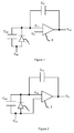
- the photodetector 1 is a photodiode which comprises a parasitic capacitor C det mounted in parallel with the photodetector 1.
- the photodetector 1 is connected to a capacitive transimpedance amplifier type reading circuit or CTIA in the English language for Capacitive Translmpedance Amplifier.
- the read circuit comprises an amplifier 2, an input of which is connected to the photodetector 1.
- the other input of the amplifier 2 is connected to a voltage source which applies the voltage V ref .
- the output of the amplifier 2 delivers a voltage signal V out representative of the current signal delivered by the photodetector 1.
- An integration capacitor Cint is connected to the amplifier in a feedback arrangement, ie it connects the output terminal and the terminal connected to the photodetector.
- the signal-to-noise ratio is particularly unfavorable in detection devices which have large photodetectors and which are configured to detect a very low flux, that is to say that the integration capacitor has a low electrical capacitance and a strong capacity of the detector.
- the subject of the invention is a detection device which has an improved signal-to-noise ratio.
- the amplifier is unbalanced so that the voltage on the first input terminal of the amplifier is offset from the voltage on the second input terminal of the amplifier by a voltage difference at least 20mV.
- the unpredictability has a negligible effect on the conversion of the light signal into an electrical signal.
- the voltage difference is between 50 and 100mV to further reduce the effects of the method of production on a very large number of photodetectors and read circuits.
- the amplifier comprises a current mirror provided with two branches mounted in shunt, one of the branches having different electrical performance of the other branch.
- one of the branches of the current mirror comprises several additional transistors connected in parallel of a main transistor, the additional transistors and the main transistor all receiving the same signal on their control electrode.
- one of the branches of the current mirror has a plurality of connection switches connected to allow or block the passage of a current from each associated additional transistor.
- first and second input terminals are respectively connected to control electrodes of first and second transistors and the first and second transistors have different electrical performances.
- first and second input terminals are respectively connected to control electrodes of the first and second transistors and that several additional transistors are connected in parallel with the first transistor, the additional transistors receiving on their control electrodes the same signal as the first transistor.
- the additional transistors are connected in parallel by means of a plurality of connection switches connected to enable or block the passage of a current from each associated additional transistor.
- the first voltage source is the second voltage source so that the reference voltage is equal to the detector voltage.
- the first voltage source and the second voltage source are formed by means of an initial voltage source supplying a resistive bridge delivering the reference voltage and the detector voltage different from the reference voltage. .
- the figure 2 illustrates a first embodiment of a detection circuit.
- the detection circuit comprises a photodetector 1 which is preferably a photodiode.
- the photodetector comprises a parasitic capacitor C det mounted in parallel with the photodetector 1.
- the photodetector generates a current representative of the observed scene.
- the photodetector can be configured to detect signals in the visible range or in the infrared range.
- the photodetector 1 is connected to a capacitive transimpedance amplifier type reading circuit or CTIA in the English language for Capacitive Translmpedance Amplifier.
- the read circuit comprises an amplifier 2, an input of which is connected to the photodetector 1.
- the other input of the amplifier 2 is connected to a voltage source which applies the voltage V ref .
- the output of the amplifier 2 delivers a voltage signal V out representative of the current signal delivered by the photodetector 1.
- An integrating capacitor C int is connected to the amplifier in a feedback circuit, that is, it connects the output terminal and the first input terminal connected to the photodetector 1.
- noise 1 + VS det VS int .
- V ref * - VS det VS int .
- V ref * and V det * represent the noise components of the voltage V ref and V det .
- the noise level is related to the ratio of the capacitors VS det VS int .
- the electrical capacitance values are related to the performance of the device and are not easily modifiable.
- the voltage V ref and the voltage V det are identical and are provided by the same voltage source so that the noise component supplied by the voltage source is correlated for the voltage V ref applied to a terminal of the amplifier and for the voltage V det applied to a terminal of the photodetector.
- the voltage V det is applied to the photodetector and the amplifier.
- the first voltage source is the second voltage source so that the reference voltage V ref is equal to the detector voltage V det .
- the operational amplifier 2 is unbalanced so as to create a voltage difference between the inverting input and the non-inverting input, that is to say between the two inputs of the amplifier.
- the voltages present on the two inputs of the operational amplifier are identical.
- the voltage V ref is applied to the second input terminal of the amplifier 2 and if the capacitor C int is discharged or lightly charged, the first input terminal of the amplifier is also at the voltage V ref which allows to polarize the photodetector 1.
- V ref voltage which allows to polarize the photodetector 1.
- the voltage difference between the two inputs is less than 10mV in absolute value.
- a detection device which comprises a matrix of photodetectors (for example 1000 photodetectors) associated with a matrix of read circuits (for example 1000 read circuits) of multiple different polarization voltages are observed.
- the operational amplifier 2 In order to ensure a more homogeneous operation of the photodetectors, it is advantageous to unbalance the operational amplifier 2 so that the difference between the inverting and non-inverting inputs is greater than or equal to 20mV and preferably in the range 50.degree. -100mV.
- the amplifier is unbalanced so that the voltage on the first input terminal of the amplifier is shifted from the voltage on the second input terminal of the amplifier of a voltage difference to less than 20mV and preferentially in the range 50-100mV.
- the imbalance is achieved so that the voltage shift is between three and six times the dispersion observed on the transistors.
- the manufacturing variations of the different amplifiers do not disturb the polarization conditions of the photodetector 1.
- the operational amplifier 2 is unbalanced so that the photodetector 1 is reverse biased. In the case where the photodetector 1 is a photodiode, this precaution makes it possible to place the photodiode on the reverse polarization plateau. If a matrix of photodetectors 1 is used in association with a read circuit array, the behavioral variations related to the polarization variation are at least partially erased.
- the first input terminal supplies the voltage V ref .
- the amplifier commonly comprising a current mirror provided with two branches mounted in shunt, it is then possible to provide that one of the branches has different electrical performance of the other branch.
- first and second input terminals are respectively connected to the control electrodes of first and second transistors T3 and T4.
- the imbalance is introduced by using first and second transistors that have different electrical performance.
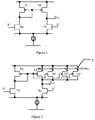
- the figure 3 illustrates a schematic embodiment of an operational amplifier.
- the operational amplifier comprises a current mirror circuit formed by the transistors T1 and T2.
- the inverting and non-inverting inputs are represented by the control electrodes receiving the V - and V + signals.
- the signal V + is applied to the control electrode of the transistor T3.
- the signal V - is applied to the control electrode of the transistor T4.
- Transistors T1 and T3 are connected in series in a first branch while transistors T2 and T4 are connected in series in a second branch. The two branches are connected bypass.
- the transistors are different between the two inputs.
- One way of producing such a device is for example to use transistors having different sizes.
- the transistors T1 and T3 receiving signals V + and V -, that is to say for example the voltage V det, have different dimensions. It is also possible to have transistors T1 and T2 having different dimensions. It is still possible to have a combination of these two embodiments as long as the two branch branches have different electrical performance.
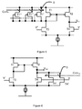
- one of the branches of the current mirror comprises several additional transistors connected in parallel of a main transistor, the additional transistors and the main transistor all receiving the same signal on their control electrode. More specifically, it is possible to provide that the branch provided with the additional transistors comprises a plurality of connection switches 3 connected to enable or block the passage of a current from each associated additional transistor.
- a plurality of additional transistors T2 ', T2 "and T2'" are connected in parallel with the main transistor T2.
- the transistors all receive the same signal on their control electrode.
- the different additional transistors are each coupled to a connection switch 3 which is configured to allow or block the passage of a current to the branch containing the transistor T2.
- These different connection switches 3 are activated separately by the signal Com T2 .
- the signal ComT2 makes it possible to choose whether one or more transistors must be connected in parallel with the transistor T2. In this way, it is possible to choose the amount of current flowing in the branch of the current mirror. The greater the number of connected transistors, the greater the current delivered. By modulating the number of transistors connected in parallel, it is possible to modulate the imbalance between the two branches of the current mirror.
- the transistors T1, T2, T2 ', T2 "and T2'" are identical so as to facilitate the manufacturing process.
- the number of series-connected transistors defines the amplitude of the imbalance.
- the imbalance is achieved on the other branch of the current mirror.
- Several transistors are connected in parallel with the main transistor T1.
- the various additional transistors T1 ', T1 "and T1"' are coupled to connection switches 3 which are activated by the signal Com T1 .
- What has been explained for the embodiment of the figure 4 also applies to the embodiment of the figure 5 by switching the transistors T1 and T2.
- the imbalance is achieved on the transistors receiving the V + and V - signals.
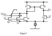
- the embodiments of the figures 6 and 7 represent assemblies for easily unbalancing the operational amplifier.
- the first and second input terminals are respectively connected to the control electrodes of first and second transistors and a plurality of additional transistors are connected in parallel with the first transistor, the additional transistors receiving on their control electrodes the same signal as the first transistor, which may be the transistor T3 or T4. More specifically, it is advantageous to provide that the additional transistors are connected in parallel by means of a plurality of connection switches 3 connected to enable or block the passage of a current from each associated additional transistor.
- the transistor T4 receives the same signal on their control electrode, here the signal V - .
- All additional transistors are also coupled to a connection switch 3 which is configured to allow or block the passage of an additional current in the branch of the operational amplifier.
- the connection switches 3 are activated by means of the signal Com T4 .
- the Com signal T4 makes it possible to define the number of transistors connected in parallel and therefore the difference in current between the two branches.
- the embodiment of the figure 7 illustrates another embodiment where the unbalance of the amplifier is realized by means of several transistors connected in parallel with the transistor T3.
- the multiple transistors connected in parallel make it possible to modulate the amount of current flowing in this branch and therefore the current difference between the two branches.
- the number of transistors involved in the transfer of the current is defined by means of the connection switches 3 and therefore by means of the signal Com T3 which activates the connection switches 3.
- the same voltage source 4 is used to deliver the voltages V ref and V det , but these two voltages are not equal.
- the voltage V ref is obtained from the voltage V det or vice versa. Both voltages are correlated to eliminate the noise component.
- the first voltage source and the second voltage source are formed by means of an initial voltage source supplying a resistive bridge delivering the reference voltage V ref and the detector voltage V det different from the reference voltage V ref .
- the voltage V ref is obtained from the voltage V det by means of a resistive bridge.
- An initial voltage source 5 is used to deliver the voltage V 1 .
- the voltage V 1 is applied to the input of the resistive bridge which delivers the voltages V ref and V det .
- the resistors R1 and R2 are connected in series between the voltage V 1 and the ground and the voltage V ref is delivered by the common terminal to the resistors R1 and R2.
- the resistors R3 and R4 are series mounted and they are together connected in parallel with the resistor R2.
- the voltage V det is delivered by the common terminal to the resistors R3 and R4.
- the reference voltage V ref may be equal to 1.5V.
- the photodetector voltage V det can be shifted from the reference voltage V ref by approximately 200mV.
- the noise level is between 50 and 100 ⁇ V.
- the integration capacitor C int may be of the order of 50 fF.
- the parasitic capacitor C det is about 900 fF.
- the correlation of the voltage sources is advantageous in cooled detection devices, for example in detection devices having an operating temperature below -50 ° C since these devices are generally used to detect low fluxes. It is possible to use photodetectors made on a substrate of Mercury, Cadmium and Tellurium, but other materials are also conceivable.
- the photodetectors are made in a first substrate made of a first semiconductor material and the reading circuits are made in a second substrate made of a second semiconductor material different from the first semiconductor material.
Landscapes
- Engineering & Computer Science (AREA)
- Power Engineering (AREA)
- Multimedia (AREA)
- Signal Processing (AREA)
- Physics & Mathematics (AREA)
- General Physics & Mathematics (AREA)
- Spectroscopy & Molecular Physics (AREA)
- Amplifiers (AREA)
Applications Claiming Priority (1)
| Application Number | Priority Date | Filing Date | Title |
|---|---|---|---|
| FR1551132A FR3032853B1 (fr) | 2015-02-12 | 2015-02-12 | Dispositif de detection ameliore |
Publications (2)
| Publication Number | Publication Date |
|---|---|
| EP3057311A1 true EP3057311A1 (de) | 2016-08-17 |
| EP3057311B1 EP3057311B1 (de) | 2020-09-02 |
Family
ID=53674020
Family Applications (1)
| Application Number | Title | Priority Date | Filing Date |
|---|---|---|---|
| EP16155440.7A Active EP3057311B1 (de) | 2015-02-12 | 2016-02-12 | Verbesserte detektionsvorrichtung |
Country Status (4)
| Country | Link |
|---|---|
| US (1) | US10066988B2 (de) |
| EP (1) | EP3057311B1 (de) |
| FR (1) | FR3032853B1 (de) |
| IL (1) | IL244094B (de) |
Families Citing this family (2)
| Publication number | Priority date | Publication date | Assignee | Title |
|---|---|---|---|---|
| WO2025021813A1 (en) | 2023-07-24 | 2025-01-30 | Trinamix Gmbh | Photodetector and method for converting illumination charges |
| CN117055672A (zh) * | 2023-08-11 | 2023-11-14 | 芯原微电子(成都)有限公司 | 电压转换电路 |
Citations (4)
| Publication number | Priority date | Publication date | Assignee | Title |
|---|---|---|---|---|
| FR2593319A1 (fr) * | 1986-01-17 | 1987-07-24 | Thomson Csf | Procede de lecture d'element photosensible constitue d'une photodiode et d'une capacite |
| US6097021A (en) * | 1997-01-06 | 2000-08-01 | Texas Instruments Incorporated | Apparatus and method for a managed integration optical sensor array |
| EP0845687B1 (de) * | 1996-11-27 | 2002-05-22 | General Electric Company | Einem grossflächigen Festkörper-Röntgenstrahlendetektor mit regelbaren Vorspannungseinstellung |
| US20140061488A1 (en) * | 2012-08-31 | 2014-03-06 | Canon Kabushiki Kaisha | Radiation imaging apparatus and radiation imaging system |
Family Cites Families (3)
| Publication number | Priority date | Publication date | Assignee | Title |
|---|---|---|---|---|
| US4889985A (en) * | 1988-10-26 | 1989-12-26 | Tektronix, Inc. | Combined optical power meter and receiver |
| US7773134B2 (en) * | 2004-03-15 | 2010-08-10 | Avago Technologies Ecbu Ip (Singapore) Pte. Ltd. | System and method for canceling dark photocurrent in a color sensor circuit |
| JP6164798B2 (ja) * | 2012-04-04 | 2017-07-19 | キヤノン株式会社 | 放射線撮像装置、放射線撮像システム、及び、放射線撮像装置の制御方法 |
-
2015
- 2015-02-12 FR FR1551132A patent/FR3032853B1/fr active Active
-
2016
- 2016-02-11 US US15/041,496 patent/US10066988B2/en active Active
- 2016-02-11 IL IL24409416A patent/IL244094B/en active IP Right Grant
- 2016-02-12 EP EP16155440.7A patent/EP3057311B1/de active Active
Patent Citations (4)
| Publication number | Priority date | Publication date | Assignee | Title |
|---|---|---|---|---|
| FR2593319A1 (fr) * | 1986-01-17 | 1987-07-24 | Thomson Csf | Procede de lecture d'element photosensible constitue d'une photodiode et d'une capacite |
| EP0845687B1 (de) * | 1996-11-27 | 2002-05-22 | General Electric Company | Einem grossflächigen Festkörper-Röntgenstrahlendetektor mit regelbaren Vorspannungseinstellung |
| US6097021A (en) * | 1997-01-06 | 2000-08-01 | Texas Instruments Incorporated | Apparatus and method for a managed integration optical sensor array |
| US20140061488A1 (en) * | 2012-08-31 | 2014-03-06 | Canon Kabushiki Kaisha | Radiation imaging apparatus and radiation imaging system |
Also Published As
| Publication number | Publication date |
|---|---|
| IL244094A0 (en) | 2016-07-31 |
| EP3057311B1 (de) | 2020-09-02 |
| US20160238446A1 (en) | 2016-08-18 |
| FR3032853B1 (fr) | 2017-02-17 |
| FR3032853A1 (fr) | 2016-08-19 |
| IL244094B (en) | 2019-10-31 |
| US10066988B2 (en) | 2018-09-04 |
Similar Documents
| Publication | Publication Date | Title |
|---|---|---|
| FR2654274A1 (fr) | Procede et circuit pour annuler la distorsion harmonique induite par une capacite non lineaire. | |
| EP2600125B1 (de) | Vorrichtung zum Erfassen von Strahlung mit einem verbesserten Beleuchtungsbereich | |
| FR2623307A1 (fr) | Source de courant a deux bornes avec compensation de temperature | |
| EP2302341A2 (de) | Detektionsschaltung mit verbessertem Blendschutz | |
| FR2558659A1 (fr) | Circuit de polarisation d'un transistor a effet de champ | |
| EP3057311B1 (de) | Verbesserte detektionsvorrichtung | |
| EP1647091B1 (de) | Spannungsverstärker mit niedrigem verbrauch | |
| EP3457566B1 (de) | Vorrichtung, die den impedanzwert eines referenzwiderstands ändert | |
| EP3819615A1 (de) | Rekonfigurierbarer ir-pixel im di- oder bdi-modus | |
| FR2623347A1 (de) | ||
| EP1313309A1 (de) | Kalibriervorrichtung für eine Video-Eingangsstufe | |
| FR2770947A1 (fr) | Amplificateur differentiel a transistor mos | |
| EP2463632B1 (de) | Erfassungsvorrichtung, die einen robusten Testkreislauf umfasst | |
| FR3018351A1 (fr) | Circuit de detection de rayonnement lumineux | |
| EP3451181B1 (de) | Schutzschaltkreis gegen hohe spannungen für einen usb-empfänger vom typ c | |
| EP0750782B1 (de) | Schnelle differenziale abtast- und halteschaltung | |
| EP0568474B1 (de) | MOS-Schaltung zum Extrahieren eines Synchronisierungssignals in einem BAS-Videosignal | |
| EP2783192B1 (de) | Detektorschaltung mit einem geräuschreduzierenden modul | |
| FR2822308A1 (fr) | Circuit pour la separation de poles reposant sur l'effet miller | |
| EP1102148A1 (de) | Niedrigtemperaturkorrigierte Spannungsgeneratoreinrichtung | |
| EP2309726B1 (de) | Detektionsschaltung mit teilweiser Umleitung des Photodetektorstroms | |
| EP1487106A1 (de) | Integrierte Schaltung zur Erzeugung von speisespannungsunabhängigen logischen Pegeln , ohne Regler im Leistungsteil und entsprechendes Kommunikationsmodul. | |
| FR2549668A1 (fr) | Circuit injecteur de sonnerie pour poste telephonique d'abonne | |
| FR2552949A1 (fr) | Circuit cascode silencieux avec zone morte |
Legal Events
| Date | Code | Title | Description |
|---|---|---|---|
| PUAI | Public reference made under article 153(3) epc to a published international application that has entered the european phase |
Free format text: ORIGINAL CODE: 0009012 |
|
| AK | Designated contracting states |
Kind code of ref document: A1 Designated state(s): AL AT BE BG CH CY CZ DE DK EE ES FI FR GB GR HR HU IE IS IT LI LT LU LV MC MK MT NL NO PL PT RO RS SE SI SK SM TR |
|
| AX | Request for extension of the european patent |
Extension state: BA ME |
|
| STAA | Information on the status of an ep patent application or granted ep patent |
Free format text: STATUS: REQUEST FOR EXAMINATION WAS MADE |
|
| 17P | Request for examination filed |
Effective date: 20170214 |
|
| RBV | Designated contracting states (corrected) |
Designated state(s): AL AT BE BG CH CY CZ DE DK EE ES FI FR GB GR HR HU IE IS IT LI LT LU LV MC MK MT NL NO PL PT RO RS SE SI SK SM TR |
|
| STAA | Information on the status of an ep patent application or granted ep patent |
Free format text: STATUS: EXAMINATION IS IN PROGRESS |
|
| 17Q | First examination report despatched |
Effective date: 20180716 |
|
| RAP1 | Party data changed (applicant data changed or rights of an application transferred) |
Owner name: LYNRED |
|
| GRAP | Despatch of communication of intention to grant a patent |
Free format text: ORIGINAL CODE: EPIDOSNIGR1 |
|
| STAA | Information on the status of an ep patent application or granted ep patent |
Free format text: STATUS: GRANT OF PATENT IS INTENDED |
|
| INTG | Intention to grant announced |
Effective date: 20200327 |
|
| RIC1 | Information provided on ipc code assigned before grant |
Ipc: H04N 5/335 20110101ALI20200314BHEP Ipc: H04N 5/378 20110101ALI20200314BHEP Ipc: H03F 3/45 20060101ALN20200314BHEP Ipc: H03F 3/08 20060101ALI20200314BHEP Ipc: H04N 5/3745 20110101AFI20200314BHEP |
|
| GRAS | Grant fee paid |
Free format text: ORIGINAL CODE: EPIDOSNIGR3 |
|
| GRAA | (expected) grant |
Free format text: ORIGINAL CODE: 0009210 |
|
| STAA | Information on the status of an ep patent application or granted ep patent |
Free format text: STATUS: THE PATENT HAS BEEN GRANTED |
|
| AK | Designated contracting states |
Kind code of ref document: B1 Designated state(s): AL AT BE BG CH CY CZ DE DK EE ES FI FR GB GR HR HU IE IS IT LI LT LU LV MC MK MT NL NO PL PT RO RS SE SI SK SM TR |
|
| REG | Reference to a national code |
Ref country code: GB Ref legal event code: FG4D Free format text: NOT ENGLISH |
|
| REG | Reference to a national code |
Ref country code: AT Ref legal event code: REF Ref document number: 1310168 Country of ref document: AT Kind code of ref document: T Effective date: 20200915 Ref country code: CH Ref legal event code: EP |
|
| REG | Reference to a national code |
Ref country code: DE Ref legal event code: R096 Ref document number: 602016043037 Country of ref document: DE |
|
| REG | Reference to a national code |
Ref country code: IE Ref legal event code: FG4D Free format text: LANGUAGE OF EP DOCUMENT: FRENCH |
|
| REG | Reference to a national code |
Ref country code: SE Ref legal event code: TRGR |
|
| REG | Reference to a national code |
Ref country code: LT Ref legal event code: MG4D |
|
| PG25 | Lapsed in a contracting state [announced via postgrant information from national office to epo] |
Ref country code: HR Free format text: LAPSE BECAUSE OF FAILURE TO SUBMIT A TRANSLATION OF THE DESCRIPTION OR TO PAY THE FEE WITHIN THE PRESCRIBED TIME-LIMIT Effective date: 20200902 Ref country code: BG Free format text: LAPSE BECAUSE OF FAILURE TO SUBMIT A TRANSLATION OF THE DESCRIPTION OR TO PAY THE FEE WITHIN THE PRESCRIBED TIME-LIMIT Effective date: 20201202 Ref country code: GR Free format text: LAPSE BECAUSE OF FAILURE TO SUBMIT A TRANSLATION OF THE DESCRIPTION OR TO PAY THE FEE WITHIN THE PRESCRIBED TIME-LIMIT Effective date: 20201203 Ref country code: NO Free format text: LAPSE BECAUSE OF FAILURE TO SUBMIT A TRANSLATION OF THE DESCRIPTION OR TO PAY THE FEE WITHIN THE PRESCRIBED TIME-LIMIT Effective date: 20201202 Ref country code: FI Free format text: LAPSE BECAUSE OF FAILURE TO SUBMIT A TRANSLATION OF THE DESCRIPTION OR TO PAY THE FEE WITHIN THE PRESCRIBED TIME-LIMIT Effective date: 20200902 Ref country code: LT Free format text: LAPSE BECAUSE OF FAILURE TO SUBMIT A TRANSLATION OF THE DESCRIPTION OR TO PAY THE FEE WITHIN THE PRESCRIBED TIME-LIMIT Effective date: 20200902 |
|
| REG | Reference to a national code |
Ref country code: NL Ref legal event code: MP Effective date: 20200902 |
|
| REG | Reference to a national code |
Ref country code: AT Ref legal event code: MK05 Ref document number: 1310168 Country of ref document: AT Kind code of ref document: T Effective date: 20200902 |
|
| PG25 | Lapsed in a contracting state [announced via postgrant information from national office to epo] |
Ref country code: LV Free format text: LAPSE BECAUSE OF FAILURE TO SUBMIT A TRANSLATION OF THE DESCRIPTION OR TO PAY THE FEE WITHIN THE PRESCRIBED TIME-LIMIT Effective date: 20200902 Ref country code: RS Free format text: LAPSE BECAUSE OF FAILURE TO SUBMIT A TRANSLATION OF THE DESCRIPTION OR TO PAY THE FEE WITHIN THE PRESCRIBED TIME-LIMIT Effective date: 20200902 Ref country code: PL Free format text: LAPSE BECAUSE OF FAILURE TO SUBMIT A TRANSLATION OF THE DESCRIPTION OR TO PAY THE FEE WITHIN THE PRESCRIBED TIME-LIMIT Effective date: 20200902 |
|
| PG25 | Lapsed in a contracting state [announced via postgrant information from national office to epo] |
Ref country code: PT Free format text: LAPSE BECAUSE OF FAILURE TO SUBMIT A TRANSLATION OF THE DESCRIPTION OR TO PAY THE FEE WITHIN THE PRESCRIBED TIME-LIMIT Effective date: 20210104 Ref country code: RO Free format text: LAPSE BECAUSE OF FAILURE TO SUBMIT A TRANSLATION OF THE DESCRIPTION OR TO PAY THE FEE WITHIN THE PRESCRIBED TIME-LIMIT Effective date: 20200902 Ref country code: SM Free format text: LAPSE BECAUSE OF FAILURE TO SUBMIT A TRANSLATION OF THE DESCRIPTION OR TO PAY THE FEE WITHIN THE PRESCRIBED TIME-LIMIT Effective date: 20200902 Ref country code: EE Free format text: LAPSE BECAUSE OF FAILURE TO SUBMIT A TRANSLATION OF THE DESCRIPTION OR TO PAY THE FEE WITHIN THE PRESCRIBED TIME-LIMIT Effective date: 20200902 Ref country code: NL Free format text: LAPSE BECAUSE OF FAILURE TO SUBMIT A TRANSLATION OF THE DESCRIPTION OR TO PAY THE FEE WITHIN THE PRESCRIBED TIME-LIMIT Effective date: 20200902 Ref country code: CZ Free format text: LAPSE BECAUSE OF FAILURE TO SUBMIT A TRANSLATION OF THE DESCRIPTION OR TO PAY THE FEE WITHIN THE PRESCRIBED TIME-LIMIT Effective date: 20200902 |
|
| PG25 | Lapsed in a contracting state [announced via postgrant information from national office to epo] |
Ref country code: AL Free format text: LAPSE BECAUSE OF FAILURE TO SUBMIT A TRANSLATION OF THE DESCRIPTION OR TO PAY THE FEE WITHIN THE PRESCRIBED TIME-LIMIT Effective date: 20200902 Ref country code: AT Free format text: LAPSE BECAUSE OF FAILURE TO SUBMIT A TRANSLATION OF THE DESCRIPTION OR TO PAY THE FEE WITHIN THE PRESCRIBED TIME-LIMIT Effective date: 20200902 Ref country code: ES Free format text: LAPSE BECAUSE OF FAILURE TO SUBMIT A TRANSLATION OF THE DESCRIPTION OR TO PAY THE FEE WITHIN THE PRESCRIBED TIME-LIMIT Effective date: 20200902 Ref country code: IS Free format text: LAPSE BECAUSE OF FAILURE TO SUBMIT A TRANSLATION OF THE DESCRIPTION OR TO PAY THE FEE WITHIN THE PRESCRIBED TIME-LIMIT Effective date: 20210102 |
|
| REG | Reference to a national code |
Ref country code: DE Ref legal event code: R097 Ref document number: 602016043037 Country of ref document: DE |
|
| PG25 | Lapsed in a contracting state [announced via postgrant information from national office to epo] |
Ref country code: SK Free format text: LAPSE BECAUSE OF FAILURE TO SUBMIT A TRANSLATION OF THE DESCRIPTION OR TO PAY THE FEE WITHIN THE PRESCRIBED TIME-LIMIT Effective date: 20200902 |
|
| PLBE | No opposition filed within time limit |
Free format text: ORIGINAL CODE: 0009261 |
|
| STAA | Information on the status of an ep patent application or granted ep patent |
Free format text: STATUS: NO OPPOSITION FILED WITHIN TIME LIMIT |
|
| 26N | No opposition filed |
Effective date: 20210603 |
|
| PG25 | Lapsed in a contracting state [announced via postgrant information from national office to epo] |
Ref country code: DK Free format text: LAPSE BECAUSE OF FAILURE TO SUBMIT A TRANSLATION OF THE DESCRIPTION OR TO PAY THE FEE WITHIN THE PRESCRIBED TIME-LIMIT Effective date: 20200902 Ref country code: SI Free format text: LAPSE BECAUSE OF FAILURE TO SUBMIT A TRANSLATION OF THE DESCRIPTION OR TO PAY THE FEE WITHIN THE PRESCRIBED TIME-LIMIT Effective date: 20200902 |
|
| PG25 | Lapsed in a contracting state [announced via postgrant information from national office to epo] |
Ref country code: MC Free format text: LAPSE BECAUSE OF FAILURE TO SUBMIT A TRANSLATION OF THE DESCRIPTION OR TO PAY THE FEE WITHIN THE PRESCRIBED TIME-LIMIT Effective date: 20200902 |
|
| REG | Reference to a national code |
Ref country code: BE Ref legal event code: MM Effective date: 20210228 |
|
| PG25 | Lapsed in a contracting state [announced via postgrant information from national office to epo] |
Ref country code: LU Free format text: LAPSE BECAUSE OF NON-PAYMENT OF DUE FEES Effective date: 20210212 Ref country code: LI Free format text: LAPSE BECAUSE OF NON-PAYMENT OF DUE FEES Effective date: 20210228 Ref country code: CH Free format text: LAPSE BECAUSE OF NON-PAYMENT OF DUE FEES Effective date: 20210228 Ref country code: IT Free format text: LAPSE BECAUSE OF FAILURE TO SUBMIT A TRANSLATION OF THE DESCRIPTION OR TO PAY THE FEE WITHIN THE PRESCRIBED TIME-LIMIT Effective date: 20200902 |
|
| PG25 | Lapsed in a contracting state [announced via postgrant information from national office to epo] |
Ref country code: IE Free format text: LAPSE BECAUSE OF NON-PAYMENT OF DUE FEES Effective date: 20210212 |
|
| PG25 | Lapsed in a contracting state [announced via postgrant information from national office to epo] |
Ref country code: BE Free format text: LAPSE BECAUSE OF NON-PAYMENT OF DUE FEES Effective date: 20210228 |
|
| REG | Reference to a national code |
Ref country code: DE Ref legal event code: R079 Ref document number: 602016043037 Country of ref document: DE Free format text: PREVIOUS MAIN CLASS: H04N0005374500 Ipc: H04N0025770000 |
|
| PG25 | Lapsed in a contracting state [announced via postgrant information from national office to epo] |
Ref country code: HU Free format text: LAPSE BECAUSE OF FAILURE TO SUBMIT A TRANSLATION OF THE DESCRIPTION OR TO PAY THE FEE WITHIN THE PRESCRIBED TIME-LIMIT; INVALID AB INITIO Effective date: 20160212 |
|
| PG25 | Lapsed in a contracting state [announced via postgrant information from national office to epo] |
Ref country code: CY Free format text: LAPSE BECAUSE OF FAILURE TO SUBMIT A TRANSLATION OF THE DESCRIPTION OR TO PAY THE FEE WITHIN THE PRESCRIBED TIME-LIMIT Effective date: 20200902 |
|
| PG25 | Lapsed in a contracting state [announced via postgrant information from national office to epo] |
Ref country code: MK Free format text: LAPSE BECAUSE OF FAILURE TO SUBMIT A TRANSLATION OF THE DESCRIPTION OR TO PAY THE FEE WITHIN THE PRESCRIBED TIME-LIMIT Effective date: 20200902 |
|
| PG25 | Lapsed in a contracting state [announced via postgrant information from national office to epo] |
Ref country code: MT Free format text: LAPSE BECAUSE OF FAILURE TO SUBMIT A TRANSLATION OF THE DESCRIPTION OR TO PAY THE FEE WITHIN THE PRESCRIBED TIME-LIMIT Effective date: 20200902 |
|
| PGFP | Annual fee paid to national office [announced via postgrant information from national office to epo] |
Ref country code: DE Payment date: 20250218 Year of fee payment: 10 |
|
| PGFP | Annual fee paid to national office [announced via postgrant information from national office to epo] |
Ref country code: SE Payment date: 20250219 Year of fee payment: 10 |
|
| PGFP | Annual fee paid to national office [announced via postgrant information from national office to epo] |
Ref country code: FR Payment date: 20250220 Year of fee payment: 10 |
|
| PGFP | Annual fee paid to national office [announced via postgrant information from national office to epo] |
Ref country code: GB Payment date: 20250220 Year of fee payment: 10 |
|
| PG25 | Lapsed in a contracting state [announced via postgrant information from national office to epo] |
Ref country code: TR Free format text: LAPSE BECAUSE OF FAILURE TO SUBMIT A TRANSLATION OF THE DESCRIPTION OR TO PAY THE FEE WITHIN THE PRESCRIBED TIME-LIMIT Effective date: 20200902 |