EP3059862B1 - Bedieneinrichtung für ein elektrokochgerät und elektrokochgerät - Google Patents
Bedieneinrichtung für ein elektrokochgerät und elektrokochgerät Download PDFInfo
- Publication number
- EP3059862B1 EP3059862B1 EP16156555.1A EP16156555A EP3059862B1 EP 3059862 B1 EP3059862 B1 EP 3059862B1 EP 16156555 A EP16156555 A EP 16156555A EP 3059862 B1 EP3059862 B1 EP 3059862B1
- Authority
- EP
- European Patent Office
- Prior art keywords
- housing
- recess
- operating device
- sensor element
- component carrier
- Prior art date
- Legal status (The legal status is an assumption and is not a legal conclusion. Google has not performed a legal analysis and makes no representation as to the accuracy of the status listed.)
- Active
Links
- 238000010411 cooking Methods 0.000 title claims description 9
- 239000000463 material Substances 0.000 claims description 44
- 239000004020 conductor Substances 0.000 claims description 16
- 229920001971 elastomer Polymers 0.000 claims description 8
- 239000000806 elastomer Substances 0.000 claims description 5
- 239000011248 coating agent Substances 0.000 claims description 3
- 238000000576 coating method Methods 0.000 claims description 3
- 238000001746 injection moulding Methods 0.000 claims description 2
- 238000000034 method Methods 0.000 claims description 2
- 229920002994 synthetic fiber Polymers 0.000 claims 4
- 238000002347 injection Methods 0.000 claims 1
- 239000007924 injection Substances 0.000 claims 1
- 239000004033 plastic Substances 0.000 description 22
- 238000003780 insertion Methods 0.000 description 4
- 230000037431 insertion Effects 0.000 description 4
- 229920002725 thermoplastic elastomer Polymers 0.000 description 4
- RYGMFSIKBFXOCR-UHFFFAOYSA-N Copper Chemical compound [Cu] RYGMFSIKBFXOCR-UHFFFAOYSA-N 0.000 description 3
- 229910052802 copper Inorganic materials 0.000 description 3
- 239000010949 copper Substances 0.000 description 3
- 230000008901 benefit Effects 0.000 description 2
- 230000000994 depressogenic effect Effects 0.000 description 2
- 238000011156 evaluation Methods 0.000 description 2
- 229920002379 silicone rubber Polymers 0.000 description 2
- 241001295925 Gegenes Species 0.000 description 1
- 238000004026 adhesive bonding Methods 0.000 description 1
- 238000005553 drilling Methods 0.000 description 1
- 229920001821 foam rubber Polymers 0.000 description 1
- 238000011031 large-scale manufacturing process Methods 0.000 description 1
- 238000004519 manufacturing process Methods 0.000 description 1
- 239000000243 solution Substances 0.000 description 1
- 238000005507 spraying Methods 0.000 description 1
- 238000011144 upstream manufacturing Methods 0.000 description 1
Images


Classifications
-
- H—ELECTRICITY
- H03—ELECTRONIC CIRCUITRY
- H03K—PULSE TECHNIQUE
- H03K17/00—Electronic switching or gating, i.e. not by contact-making and –breaking
- H03K17/94—Electronic switching or gating, i.e. not by contact-making and –breaking characterised by the way in which the control signals are generated
- H03K17/96—Touch switches
- H03K17/962—Capacitive touch switches
-
- H—ELECTRICITY
- H03—ELECTRONIC CIRCUITRY
- H03K—PULSE TECHNIQUE
- H03K17/00—Electronic switching or gating, i.e. not by contact-making and –breaking
- H03K17/94—Electronic switching or gating, i.e. not by contact-making and –breaking characterised by the way in which the control signals are generated
- H03K17/96—Touch switches
- H03K2017/9602—Touch switches characterised by the type or shape of the sensing electrodes
-
- H—ELECTRICITY
- H03—ELECTRONIC CIRCUITRY
- H03K—PULSE TECHNIQUE
- H03K2217/00—Indexing scheme related to electronic switching or gating, i.e. not by contact-making or -breaking covered by H03K17/00
- H03K2217/94—Indexing scheme related to electronic switching or gating, i.e. not by contact-making or -breaking covered by H03K17/00 characterised by the way in which the control signal is generated
- H03K2217/96—Touch switches
- H03K2217/9607—Capacitive touch switches
- H03K2217/960755—Constructional details of capacitive touch and proximity switches
- H03K2217/96076—Constructional details of capacitive touch and proximity switches with spring electrode
Definitions
- the invention relates to an operating device and an electric cooking appliance with such an operating device.
- a sensor element device for a capacitive touch switch which has an illuminated display with a light source.
- a frame-like body made of plastic sits on an annular body made of elastic, electrically conductive plastic, both of which are plugged into an LED as a light source.
- the disadvantage here is that fastening is not possible with pinpoint accuracy because, above all, it is not easy to attach the elastic plastic in the form of a foam rubber to a printed circuit board in a precisely positioned manner.
- WO 2004/040762 A1 shows another operating device with a sensor element device with a capacitive touch switch.
- An elastic, electrically conductive plastic body is provided here, the top of which rests against the underside of a cover plate.
- a plug-in section protrudes from its underside, which is undercut and which can be plugged into an opening on a circuit board. By protruding It cannot easily be pulled off the barb.
- An electrical connection to the plastic body can also be made here via the circuit board.
- a further operating device emerges with a sensor element device with a capacitive touch switch, which has an electrically conductive and translucent plastic body.
- a sensor element device with a capacitive touch switch which has an electrically conductive and translucent plastic body.
- it can have latching projections that protrude on its underside and are inserted into openings in a printed circuit board.
- the plastic body for electrical contacting rests on contact fields on the top of a circuit board.
- connection leg is tapered and surrounded with electrically conductive rubber in an area to be inserted into a hole in the circuit board.
- electrically conductive rubber is pressed from above against the conductor track. Part of the rubber is pressed into the opening.
- the invention is based on the object of creating a control device and an electric cooking appliance mentioned at the beginning with which problems of the prior art can be avoided and, in particular, it is possible to create a practical design that can also be produced precisely and at low cost in large-scale production and can also be assembled automatically if possible.
- the sensor element device has an upper side which points to the underside of a control panel or an operating panel of the operating device, which form an operating surface. It may even be attached to it. Furthermore, the sensor element device can have a luminous display with a luminous means, wherein a luminous direction can point towards the underside of the control panel, if possible towards the irradiation thereof.
- a housing is provided or the sensor element device has a housing.
- the housing can have fastening means, wherein the two can together form a structural unit. Under certain circumstances, they can even be designed in one piece as a structural unit, which is explained in more detail below.
- an electrically conductive plastic is provided at least in the area towards the top, with a course at least partially along an outer edge of the housing or the structural unit.
- This electrically conductive plastic forms the functional capacitive sensor element for the capacitive touch switch on the control panel or control surface, through which the approaching or placing of a finger on the top of the control panel above the sensor element device or the capacitive sensor element is recognized and evaluated in a known manner can be, see for example the DE 102012010321 A1 .
- an electrically conductive connection is provided as contacting or extends to the component carrier and to a control and / or evaluation unit.
- This electrical connection or contact or a connection to the capacitive sensor element can be designed in various ways, as will be explained in more detail below.
- the housing has electrically conductive and elastic contacting material on its lower area or on its underside, which material can preferably protrude beyond the underside of the housing to rest on the flat component carrier, which is advantageously a printed circuit board or circuit board.
- the flat component carrier In the area of this contacting material on the housing or directly below it, the flat component carrier has a contact field which is in particular applied permanently to the flat component carrier.
- This contact field consists of electrically conductive material, advantageously copper, and has an electrical connection to a further component on the component carrier, in particular a microcontroller or the like. as a control or, if necessary, an upstream connection with passive components.
- the component carrier has a recess on the contact field where the contacting material rests against the contact field.
- the recess in the contact field is covered with the conductor material, the conductor material running into the recess according to the shape of the recess, advantageously as a coating, and consequently having the same contour or preferably covering the surface of the recess.
- an operating device which, on the one hand, has a housing that can surround a lighting means for an illuminated display. On its upper side it has a sensor element for the capacitive touch switch that belongs to the structural unit. Furthermore, the housing can have the fastening means in order to be fastened to a component carrier, preferably without tools. At the same time, electrical contact should be made as an electrical connection for the capacitive sensor element.
- the aforementioned assembly which is quick and as automated as possible, is possible, which is particularly advantageous in the case of operating devices with a large number of such sensor element devices.
- the recess is advantageously an opening or a hole through the component carrier, advantageously with a constant diameter and / or cross section, that is to say cylindrical. It is particularly advantageous a round cylindrical shape.
- the recess can also be just a depression, for example partially spherical or conical.
- the diameter of the recess in the component carrier can be 40% to 95% of the diameter of the contacting material on the underside of the housing, preferably 60% to 85%, particularly preferably 70% to 80%. In any case, the contacting material can clearly overlap the recess, on all sides.
- the cross-sectional area of the recess in the component carrier has 40% to 95% of the cross-sectional area of the contacting material on the underside of the housing, in particular 60% to 85%, preferably 70% to 80%.
- the electrically conductive elastic contacting material is an elastomer, for example as a silicone elastomer or as a thermoplastic elastomer (TPE). It can have a hardness of 30 to 90 Shore A, preferably 40 to 50 or 65 to 70. It can thus be pressed together by a relatively low pressure force and rest well against the contact field with simultaneous spring action. It can be particularly advantageous to provide that mainly or even only the contacting material is pressed against the contact field or the component carrier, but not the other housing or the other structural unit.
- TPE thermoplastic elastomer
- the electrically conductive plastic for the sensor element in particular if it is elastic, to protrude a little beyond the top of the housing. This can be around 1 ⁇ m to 1 mm or 2 mm, advantageously around 50 ⁇ m to 500 ⁇ m.
- the protrusion is therefore very small and should only be such that the other upper side of the housing runs just below the control panel with a slight pressure.
- the electrically conductive plastic for the sensor element is preferably generally an elastomer.
- the electrical contact for the electrical connection of said sensor element to the component carrier in the lower region of the structural unit has the same plastic as the sensor element.
- An electrical contact to the electrically conductive plastic on the upper side as a sensor element can in particular also have an electrically conductive plastic, which can be applied as a partially or completely continuous layer on the outside of the housing or the structural unit.
- it is the same electrically conductive plastic in all three cases, which is provided both on the top as a sensor element and on the bottom as electrical contact to a contact field on the component carrier and as an electrical connection between the two areas . It is also advantageously applied in a single step by a corresponding spraying process.
- the electrical contact on the underside to the component carrier can be relatively small, in particular have dimensions of 1 mm to 5 mm in width. The electrical connection between them can be of a similar size, but can also run around completely.
- the housing is pressed so strongly against the component carrier in the installed state that the contacting material is pressed far into the recess at least 5% to 50% of the diameter of the recess.
- the contacting material is at least partially in contact with the conductor material in the recess. This is independent of the shape of the recess.
- the contacting material can be 3% to 30%, preferably 5% to 10%, of the diameter of the breakthrough or the hole extend or extend into an inner wall coated with conductor material.
- contacting material can be provided in several, advantageously two, separate areas, which is pressed in the same way on each contact field with a recess underneath and thus into the recess.
- the electrically conductive plastic as a capacitive sensor element on the top runs along at least one side with a polygonal cross section of the housing or the structural unit, preferably a square or rectangular cross section. These are advantageously two or three sides, so that the capacitive sensor element formed thereby becomes larger or more sensitive and effective. It advantageously runs around four sides or is designed entirely around it, that is, as a kind of frame. The size should be approximately such that placing a finger on the top of the control panel can be easily recognized, for example from 5 x 5 mm to 15 x 15 mm.
- the contacting material can form a kind of at least partially circumferential shoulder on the underside for electrical contacting, preferably completely circumferentially. With this shoulder, the housing can be pressed against the contact field or contacts on the component carrier as an electrical connection.
- contacting material can be provided in two or more areas that are separate from one another, which is pressed in each case in the same way onto a contact field with a recess underneath.
- the electrically conductive plastic is advantageously injected onto the housing, at least that on the top and / or that on the bottom.
- Multi-component syringes can be advantageous here, in particular as 2K or 3K syringes.
- the housing in a further embodiment of the invention, it is possible for the housing to have a light guide body on its upper side or towards the upper side, which extends over the illuminant.
- the housing can therefore not only surround the illuminant like a ring, but also the light guide body, at least in a lower area.
- the light guide body can also form a kind of diffuser for the light, around a uniformly illuminated symbol display or illuminated display to accomplish.
- it can have corresponding light-collecting properties, in particular also by designing its lower side as a light entry side. It can also be produced together with the housing in a multi-component injection molding process, as mentioned above, and be an integral part.
- the fastening means can have at least one downwardly projecting fastening element which can be inserted into a correspondingly formed recess in the component carrier. It is advantageous to have two fasteners for a secure and twist-free fastening.
- the fastening members can particularly advantageously have different cross sections in the insertion direction or in the longitudinal direction, so that confusion of the insertion position is avoided.
- a fastening member can be designed for self-retaining insertion, for example by clamping due to larger cross-sections or by barbs or latching hooks, so that other fastenings such as gluing or the like. can be omitted.
- the operating device has a component carrier, on which at least one sensor element device described above is arranged and / or fastened. Furthermore, the sensor element device is also electrically contacted on the component carrier, in particular as a connection for the capacitive sensor element and, if applicable, the lighting means.
- the operating device also has an aforementioned operating field, on the underside of which the sensor element device rests. A corresponding control can take place by placing a finger on the control panel, as is known to the person skilled in the art from the aforementioned prior art.
- control device is provided for a hob, so that the control panel can be a hob plate of the hob.
- the control panel can be a hob plate of the hob.
- sensor element devices can be provided on a component carrier under the hob plate and enable various switching functions.
- a sensor element device 11 for an operating device which has a housing 22 with an upper side 20, is shown in lateral section.
- the housing 22 has a lower part 21, from which fastening pins 24a and 24b with different cross-sections protrude as fastening means, the lower part 21 being made of opaque plastic.
- An upper part of the housing 22 is formed by a light guide body 28 made of translucent plastic.
- a recess 26 is provided both in the lower part 21 and in the light guide body 28 of the housing 22.
- An LED or a light source can be arranged therein.
- a circumferential collar 30 is integrally formed on the upper outside of the housing 22 or the light guide body 28.
- the collar 30 consists of elastic and electrically conductive plastic, preferably an elastomer, for example an aforementioned electrically conductive silicone elastomer or electrically conductive TPE, and is advantageously attached to the housing 22 or the light guide body 28 is molded on.
- the circumferential collar 30 also forms the capacitive sensor element 31 mentioned at the beginning. As can be seen, the collar 30 protrudes somewhat over the top 20, for example 50 ⁇ m to 100 ⁇ m.
- strip-like electrical connection contacts 33a and 33b are formed on the outside of the housing 22 on the left and right. At the bottom, they each merge into a left and a right electrical contact 35a and 35b made of the aforementioned elastic and electrically conductive contact material, preferably as an elastomer.
- the contacts 35a and 35b have on their undersides surfaces 35a 'and 35b' which are preferably generally flat.
- collar 30, connection contact 33 and contact 35 are advantageously made from the same material, particularly advantageously the aforementioned TPE, and can advantageously be made in one piece.
- the capacitive sensor element 31 can be electrically contacted below at the contacts 35a and 35b, which will be explained in more detail below.
- the contacts 35a and 35b can protrude somewhat beyond the underside of the lower part 21, for example 50 ⁇ m to 200 ⁇ m.
- a printed circuit board 37 is provided as a component carrier under the housing 22.
- the circuit board 37 has holes 39a and 39b for inserting the two fastening pins 24a and 24b, which are advantageously drilled round.
- the printed circuit board 37 has two through bores 40a and 40b, which advantageously likewise have a circular cross section and are thus round cylindrical. Such a production of holes or through-bores in the circuit board 37 is most easily carried out by drilling.
- the through bores 40a and 40b are provided in the area of contact fields 42a and 42b on the upper side of the circuit board 37.
- These contact fields 42a and 42b can be round or circular, alternatively also rectangular or square or generally of any shape.
- conductor tracks that are connected to a controller or evaluation, as is known from the prior art and in Fig. 4 is indicated.
- this conductor material is also provided along the through bores 40a and 40b down to the bottom in the manner of a conventional through-hole connection 43a and 43b. It is therefore even possible under certain circumstances to make electrical contact to the contact fields 42a and 42b and thus also to the capacitive sensor element 31 along the underside of the circuit board 37.
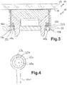
- FIG. 2 it can be seen how the housing 22 with the fastening pins 24a and 24b is inserted into the printed circuit board 37 or the corresponding holes 39a and 39b thereof.
- the surfaces 35a 'and 35b' or undersides of the contacts 35a and 35b are still located a little above the contact fields 42a and 42b. From the Fig. 2 Above all, the overlap of the surfaces 35a 'and 35b' with the contact fields 42a and 42b can be seen.
- Fig. 3 an entire operating device 14 or a section from a hob 16 is shown.
- the circuit board 37 with the housing 22 on it is now pressed against an underside 18 of a hob plate 17 as a cover or control panel and thus control surface in such a way that the capacitive sensor element 31 rests well with its substantially entire top on this underside.
- the contacts 35a and 35b are pressed with their surfaces 35a 'and 35b' against the contact fields 42a and 42b. Thus, they rest on their upper sides in order to establish electrical contact.
- a part of them is pressed into the vias 43a and 43b, which is evident from the Fig. 5 can be seen more clearly in a schematic enlargement.
- the elastic plastic material of the contacts 35a and 35b can be pressed in several 100 ⁇ m with a diameter of the through holes 40a and 40b or the through contacts 43a and 43b of 1 mm to 2 mm. This means that over a depth of 50 ⁇ m to 150 ⁇ m the contacting material rests against the plated-through holes 43a and 43b in the upper region.
- the contact area of the in the Figs. 1 to 3 horizontal plane also expanded in the vertical direction.
- Fig. 6 shows that with aged contacting material, which may still have a certain elasticity, but no longer has resilient properties, when the sensor element device 11 or the housing 22 is lifted from the circuit board 37, the electrical contact is still maintained by touching in the vertical direction . This no longer applies to larger or stronger movements. At least in the case of a slight lifting in the range of a maximum of 100 ⁇ m, however, the electrical contact is still given, namely in this aforementioned vertical range.
- the Fig. 4 still more or less in plan view according to the Fig. 3 shows how with a round configuration of the contact field 42a, from which a conductor track 44a extends downwards, and a round through-hole 40a and thus also a round through-hole 43a, a round contact 35a made of the elastic contacting material rests.
- the arrangement does not have to be concentric, in particular not the contact 35a with regard to the through-contact 43a or the through-hole 40a or the contact field 42a. But it is quite possible.
- the surfaces 35a 'and 35b' of the contacts 35a and 35b should rest on the contact fields 42a and 42b in such a way that they completely overlap the plated-through holes 43. In this way, the contacting material of the contacts 35 can be pressed well into the respective through-contact 43.
Landscapes
- Switches That Are Operated By Magnetic Or Electric Fields (AREA)
- Push-Button Switches (AREA)
Description
- Die Erfindung betrifft eine Bedieneinrichtung sowie ein Elektrokochgerät mit einer solchen Bedieneinrichtung.
- Aus der
DE 102009036162 A1 ist eine Sensorelementeinrichtung für einen kapazitiven Berührungsschalter bekannt, welche eine Leuchtanzeige mit Leuchtmittel aufweist. Ein rahmenartiger Körper aus Kunststoff sitzt auf einem Ringkörper aus elastischem, elektrisch leitfähigem Kunststoff, wobei beide über eine LED als Leuchtmittel gesteckt sind. Hierbei besteht der Nachteil, dass eine Befestigung nicht punktgenau möglich ist, weil vor allem die Anbringung des elastischen Kunststoffs in Form eines Schaumgummis positionsgenau auf einer Leiterplatte nicht leicht ist. - Aus der
DE 102012010321 A1 ist eine weitere Bedieneinrichtung mit einer Sensorelementeinrichtung mit einem kapazitiven Berührungsschalter bekannt. - Aus der
DE 102013213034 A1 ist eine nochmals weitere Bedieneinrichtung mit einer Sensorelementeinrichtung mit einem kapazitiven Berührungsschalter bekannt, die ähnlich wie die zuvor genannteDE 102012010321 A1 ausgebildet ist. Hier erfolgt eine elektrische Kontaktierung durch ein elektrisch leitfähiges Bedienelementgehäuse der Sensorelementeinrichtung. An seiner Oberseite kontaktiert es ein kapazitives Sensorelement. Eine elektrische Kontaktierung nach unten erfolgt dadurch, dass Haltefüße aus elektrisch leitfähigem Material des Bedienelementgehäuses in Öffnungen in einer Leiterplatte eingesteckt sind. Dabei kann ein auf der Oberseite der Leiterplatte angeordnetes Kontaktfeld elektrisch kontaktiert werden. Zusätzlich ist die Innenwandung der Öffnungen mit Kupfer überzogen und der Passsitz der eingesteckten Haltefüße stellt die elektrische Kontaktierung her. Die Haltefüße für das Bedienelementgehäuse sollen stabil sein, um ihre Befestigungsfunktion erfüllen zu können. - Aus der
WO 2004/040762 A1 geht eine weitere Bedieneinrichtung mit einer Sensorelementeinrichtung mit einem kapazitiven Berührungsschalter hervor. Hier ist ein elastischer elektrisch leitfähiger Kunststoffkörper vorgesehen, der mit seiner Oberseite gegen die Unterseite einer Abdeckplatte anliegt. An seiner Unterseite steht ein Steckabschnitt hervor, der hinterschnitten ist und der in eine Öffnung auf einer Leiterplatte eingesteckt werden kann. Durch abstehende Widerhaken kann er nicht so leicht wieder abgezogen werden. Hier kann auch eine elektrische Verbindung an den Kunststoffkörper über die Leiterplatte erfolgen. - Aus der
EP 2 355 356 A1 geht eine weitere Bedieneinrichtung hervor mit einer Sensorelementeinrichtung mit einem kapazitiven Berührungsschalter, die einen elektrisch leitfähigen und lichtdurchlässigen Kunststoffkörper aufweist. In einer Ausgestaltung kann er an seiner Unterseite abstehende Rastvorsprünge aufweisen, die in Öffnungen einer Leiterplatte eingesteckt sind. Direkt daneben liegt der Kunststoffkörper zur elektrischen Kontaktierung an Kontaktfeldern auf der Oberseite einer Leiterplatte an. - Aus der
JP 2005276528 A - Der Erfindung liegt die Aufgabe zugrunde, eine eingangs genannte Bedieneinrichtung sowie ein Elektrokochgerät zu schaffen, mit denen Probleme des Standes der Technik vermieden werden können, und es insbesondere möglich ist, eine praxistaugliche Ausführung zu schaffen, die auch großserientechnisch präzise und zu günstigen Kosten herstellbar ist sowie möglichst auch automatisiert montiert werden kann.
- Gelöst wird diese Aufgabe durch eine Bedieneinrichtung mit den Merkmalen des Anspruchs 1 sowie ein Elektrokochgerät mit den Merkmalen des Anspruchs 12. Vorteilhafte sowie bevorzugte Ausgestaltungen der Erfindung sind Gegenstand der weiteren Ansprüche und werden im Folgenden näher erläutert. Dabei werden manche der genannten Merkmale nur für die Bedieneinrichtung oder nur für das Elektrokochgerät genannt. Sie sollen jedoch unabhängig davon sowohl für die Bedieneinrichtung als auch für das Elektrokochgerät selbstständig gelten können.
- Es ist vorgesehen, dass die Sensorelementeinrichtung eine Oberseite aufweist, die zur Unterseite eines Bedienfeldes oder einer Bedienblende der Bedieneinrichtung, die eine Bedienfläche bilden, hin weist. Eventuell kann sie sogar daran angelegt sein. Des Weiteren kann die Sensorelementeinrichtung eine Leuchtanzeige mit einem Leuchtmittel aufweisen, wobei eine Leuchtrichtung zur Unterseite der Bedienblende hin weisen kann, möglichst zu dessen Durchstrahlung.
- Des Weiteren ist vorgesehen, dass ein Gehäuse vorgesehen ist bzw. die Sensorelementeinrichtung ein Gehäuse aufweist. Zur Befestigung der Sensorelementeinrichtung an einem Bauteilträger kann das Gehäuse Befestigungsmittel aufweisen, wobei die beiden zusammen eine Baueinheit bilden können. Unter Umständen können sie sogar einstückig als Baueinheit ausgebildet sein, was nachfolgend näher erläutert wird. Außen an dem Gehäuse bzw. der Baueinheit ist zumindest in dem Bereich zur Oberseite hin ein elektrisch leitfähiger Kunststoff vorgesehen, mit einem Verlauf zumindest teilweise entlang eines Außenrandes des Gehäuses bzw. der Baueinheit. Dieser elektrisch leitfähige Kunststoff bildet das funktionale kapazitive Sensorelement für den kapazitiven Berührungsschalter an dem Bedienfeld bzw. der Bedienfläche, durch welches das Annähern oder Auflegen eines Fingers auf die Oberseite des Bedienfeldes oberhalb der Sensorelementeinrichtung bzw. des kapazitiven Sensorelements auf bekannte Art und Weise erkannt und ausgewertet werden kann, siehe beispielsweise die
DE 102012010321 A1 . Von dem elektrisch leitfähigen Kunststoff an der Oberseite in Richtung zur Unterseite auf den Bauteilträger zu ist eine elektrisch leitfähige Verbindung als Kontaktierung vorgesehen bzw. erstreckt sich an den Bauteilträger und an eine Ansteuerung und/oder Auswertung. Diese elektrische Verbindung bzw. Kontaktierung bzw. ein Anschluss an das kapazitive Sensorelement kann verschiedenartig ausgebildet sein, wie nachfolgend noch näher erläutert wird. - Das Gehäuse weist an seinem unteren Bereich oder an seiner Unterseite elektrisch leitfähiges und elastisches Kontaktierungsmaterial auf, das vorzugsweise über die Unterseite des Gehäuses überstehen kann zur Anlage auf dem flächigen Bauteilträger, der vorteilhaft eine Leiterplatte oder Platine ist. Der flächige Bauteilträger weist im Bereich dieses Kontaktierungsmaterials am Gehäuse oder direkt unterhalb davon ein Kontaktfeld auf, das insbesondere unlösbar auf den flächigen Bauteilträger aufgebracht ist. Dieses Kontaktfeld besteht aus elektrisch leitfähigem Material, vorteilhaft Kupfer, und weist eine elektrische Verbindung an ein weiteres Bauteil auf dem Bauteilträger auf, insbesondere einen Microcontroller odgl. als Steuerung oder ggf. eine Vorschaltung mit passiven Bauteilen.
- Der Bauteilträger weist an dem Kontaktfeld dort, wo das Kontaktierungsmaterial an dem Kontaktfeld anliegt, eine Ausnehmung auf. Die Ausnehmung im Kontaktfeld ist mit dem Leitermaterial bedeckt, wobei das Leitermaterial in die Ausnehmung hinein verläuft entsprechend der Form der Ausnehmung, vorteilhaft als Beschichtung, und demzufolge dieselbe Kontur aufweist bzw. vorzugsweise die Oberfläche der Ausnehmung bedeckt.
- Mit der Erfindung kann somit eine Bedieneinrichtung geschaffen werden, welche einerseits ein Gehäuse aufweist, das ein Leuchtmittel für eine Leuchtanzeige umgeben kann. An seiner Oberseite hin weist es ein Sensorelement auf für den kapazitiven Berührungsschalter, der zu der Baueinheit gehört. Des Weiteren kann das Gehäuse die Befestigungsmittel aufweisen, um vorzugsweise werkzeuglos an einem Bauteilträger befestigt zu werden. Dabei soll gleichzeitig eine elektrische Kontaktierung als elektrischer Anschluss des kapazitiven Sensorelements erfolgen. So ist eben die zuvor genannte schnelle und möglichst automatisierte Montage möglich, was vor allem bei Bedieneinrichtungen mit einer Vielzahl von solchen Sensorelementeinrichtungen von großem Vorteil ist.
- Die Ausnehmung ist vorteilhaft ein Durchbruch oder ein Loch durch den Bauteilträger, vorteilhaft mit gleichbleibendem Durchmesser und/oder Querschnitt, also zylindrisch. Besonders vorteilhaft ist es eine rundzylindrische Form. Alternativ kann die Ausnehmung auch nur eine Vertiefung sein, beispielsweise teilkugelförmig oder kegelförmig.
- Der Durchmesser der Ausnehmung im Bauteilträger kann 40% bis 95% des Durchmessers des Kontaktierungsmaterials an der Unterseite des Gehäuses aufweist, bevorzugt 60% bis 85%, besonders bevorzugt 70% bis 80%. Jedenfalls kann das Kontaktierungsmaterial die Ausnehmung deutlich überlappen, und zwar an allen Seiten.
- Die Querschnittsfläche der Ausnehmung im Bauteilträger 40% bis 95% der Querschnittsfläche des Kontaktierungsmaterials an der Unterseite des Gehäuses aufweist, insbesondere 60% bis 85%, bevorzugt 70% bis 80%.
- Bei der Erfindung ist das elektrisch leitfähige elastische Kontaktierungsmaterial ein Elastomer, beispielsweise als Silikonelastomer oder als thermoplastisches Elastomer (TPE). Es kann eine Härte von 30 bis 90 Shore A aufweisen, vorzugsweise 40 bis 50 oder 65 bis 70. So kann es durch eine relativ geringe Andruckkraft zusammengepresst werden und gut an dem Kontaktfeld anliegen bei gleichzeitiger Federwirkung. Dabei kann besonders vorteilhaft vorgesehen sein, dass hauptsächlich oder sogar nur das Kontaktierungsmaterial an dem Kontaktfeld bzw. an dem Bauteilträger angedrückt ist, nicht jedoch das sonstige Gehäuse bzw. die sonstige Baueinheit.
- In weiterer vorteilhafter Ausgestaltung der Erfindung ist es möglich, dass der elektrisch leitfähige Kunststoff für das Sensorelement, insbesondere wenn er elastisch ist, die Oberseite des Gehäuses ein kleines Stück überragt. Dies kann um etwa 1 µm bis 1 mm oder 2 mm sein, vorteilhaft um 50 µm bis 500 µm. Der Überstand ist also sehr gering und sollte eben nur so sein, dass bei leichter Andruckkraft die sonstige Oberseite des Gehäuses knapp unter dem Bedienfeld verläuft. Vorzugsweise ist der elektrisch leitfähige Kunststoff für das Sensorelement allgemein ein Elastomer.
- Es kann vorgesehen sein, dass die elektrische Kontaktierung zur elektrischen Verbindung des genannten Sensorelements an den Bauteilträger im unteren Bereich der Baueinheit denselben Kunststoff aufweist wie das Sensorelement. Eine elektrische Kontaktierung zu dem elektrisch leitfähigen Kunststoff an der Oberseite als Sensorelement kann insbesondere ebenfalls einen elektrisch leitfähigen Kunststoff aufweisen, der als teilweise oder vollständig durchgängige Schicht an der Außenseite des Gehäuses bzw. der Baueinheit aufgebracht sein kann. In einer besonders vorteilhaften Ausgestaltung der Erfindung ist es in allen drei Fällen derselbe elektrisch leitfähige Kunststoff, der also sowohl an der Oberseite als Sensorelement vorgesehen ist als auch an der Unterseite als elektrische Kontaktierung an ein Kontaktfeld auf dem Bauteilträger sowie als elektrische Verbindung zwischen den beiden Bereichen. Vorteilhaft wird er auch in einem einzigen Schritt durch einen entsprechenden Spritzvorgang aufgebracht. Die elektrische Kontaktierung an der Unterseite zum Bauteilträger hin kann relativ klein sein, insbesondere Abmessungen von 1 mm bis 5 mm in der Breite aufweisen. Die elektrische Verbindung dazwischen kann ähnlich groß sein, kann aber auch vollständig umlaufen.
- Das Gehäuse ist erfindungsgemäß im montierten Zustand derart stark gegen den Bauteilträger gedrückt, dass das Kontaktierungsmaterial mindestens 5% bis 50% des Durchmessers der Ausnehmung weit in die Ausnehmung hinein gedrückt ist. Dabei liegt das Kontaktierungsmaterial zumindest teilweise an dem Leitermaterial auch in der Ausnehmung an. Dies ist unabhängig davon, welche Form die Ausnehmung aufweist.
- Vor allem wenn die Ausnehmung ein zylindrischer Durchbruch oder ein zylindrisches Loch ist, kann das Kontaktierungsmaterial 3% bis 30%, vorzugsweise 5% bis 10%, des Durchmessers des Durchbruchs oder des Lochs weit an einer mit Leitermaterial beschichteten Innenwandung verlaufen bzw. sich hinein erstrecken.
- An der Unterseite des Gehäuses kann in mehreren, vorteilhaft zwei, voneinander getrennten Bereichen Kontaktierungsmaterial vorgesehen sein, das auf jeweils gleiche Art und Weise an jeweils einem Kontaktfeld mit Ausnehmung darunter und somit in die Ausnehmung hinein angedrückt ist.
- Der elektrisch leitfähige Kunststoff als kapazitives Sensorelement an der Oberseite läuft bei einem mehreckigen Querschnitt des Gehäuses bzw. der Baueinheit, vorzugsweise ein viereckiger bzw. rechteckiger Querschnitt, an mindestens einer Seite entlang. Vorteilhaft sind dies zwei oder drei Seiten, so dass das davon gebildete kapazitive Sensorelement größer wird bzw. empfindlicher und wirksamer. Vorteilhaft läuft es an vier Seiten um bzw. ist ganz umlaufend ausgebildet, also als eine Art Rahmen. Die Größe sollte dabei in etwa so sein, dass ein Auflegen eines Fingers an der Oberseite des Bedienfeldes gut erkannt werden kann, also beispielsweise von 5 x 5 mm bis 15 x 15 mm.
- In vorteilhafter Ausgestaltung der Erfindung kann das Kontaktierungsmaterial an der Unterseite zur elektrischen Kontaktierung eine Art zumindest teilweise umlaufenden Absatz bilden, vorzugsweise ganz umlaufend. Mit diesem Absatz kann das Gehäuse gegen das Kontaktfeld oder Kontaktierungen auf dem Bauteilträger gedrückt werden als elektrischer Anschluss.
- An der Unterseite des Gehäuses kann in zwei oder mehr voneinander getrennten Bereichen Kontaktierungsmaterial vorgesehen sein, das auf jeweils gleiche Art und Weise an jeweils einem Kontaktfeld mit Ausnehmung darunter angedrückt ist.
- Der elektrisch leitfähige Kunststoff wird vorteilhaft an das Gehäuse angespritzt, zumindest der an der Oberseite und/oder der an der Unterseite. Hier kann ein Mehrkomponentenspritzen vorteilhaft sein, insbesondere als 2K- oder als 3K-Spritzen.
- In weiterer Ausgestaltung der Erfindung ist es möglich, dass das Gehäuse an seiner Oberseite bzw. zur Oberseite hin einen Lichtleitkörper aufweist, der über dem Leuchtmittel verläuft. Das Gehäuse kann also nicht nur das Leuchtmittel ringartig umgeben, sondern auch den Lichtleitkörper, zumindest in einem unteren Bereich. Der Lichtleitkörper kann dabei auch eine Art Diffusor bilden für das Licht, um eine gleichmäßig ausgeleuchtete Symbolanzeige oder Leuchtanzeige zu schaffen. Des Weiteren kann er, insbesondere auch durch Ausgestaltung an seiner unteren Seite als Lichteintrittsseite, entsprechende Lichtsammeleigenschaften aufweisen. Er kann auch in einem Mehrkomponentenspritzvorgang, wie eingangs genannt, zusammen mit dem Gehäuse hergestellt werden und integraler Bestandteil sein.
- Die Befestigungsmittel können mindestens ein nach unten abstehendes Befestigungsglied aufweisen, welches in eine entsprechend ausgebildete Ausnehmung in dem Bauteilträger eingesteckt werden kann. Vorteilhaft sind es zwei Befestigungsglieder für eine sichere und verdrehfreie Befestigung. Die Befestigungsglieder können besonders vorteilhaft unterschiedliche Querschnitte in Einsteckrichtung bzw. Längsrichtung aufweisen, so dass eine Verwechslung der Einsteckposition vermieden wird. Schließlich kann ein Befestigungsglied zum selbsthalternden Einstecken ausgebildet sein, beispielsweise durch Klemmung aufgrund größerer Querschnitte oder durch Widerhaken oder Rasthaken, so dass sonstige Befestigungen wie Kleben odgl. entfallen können.
- Die Bedieneinrichtung weist einen Bauteilträger auf, auf dem mindestens eine vorbeschriebene Sensorelementeinrichtung angeordnet ist und/oder befestigt ist. Des Weiteren ist die Sensorelementeinrichtung an dem Bauteilträger auch elektrisch kontaktiert, insbesondere als Anschluss des kapazitiven Sensorelements und ggf. des Leuchtmittels. Die Bedieneinrichtung weist auch ein vorgenanntes Bedienfeld auf, an dessen Unterseite die Sensorelementeinrichtung anliegt. Durch Auflegen eines Fingers auf das Bedienfeld kann eine entsprechende Steuerung erfolgen, wie dies dem Fachmann aus dem vorgenannten Stand der Technik bekannt ist.
- In besonders vorteilhafter Ausgestaltung der Erfindung ist die Bedieneinrichtung für ein Kochfeld vorgesehen, so dass das Bedienfeld eine Kochfeldplatte des Kochfeldes sein kann. Dabei können eben mehrere Sensorelementeinrichtungen auf einem Bauteilträger unter der Kochfeldplatte vorgesehen sein und verschiedene Schaltfunktionen ermöglichen.
- Diese und weitere Merkmale gehen außer aus den Ansprüchen auch aus der Beschreibung und den Zeichnungen hervor, wobei die einzelnen Merkmale jeweils für sich allein oder zu mehreren in Form von Unterkombinationen bei einer Ausführungsform der Erfindung und auf anderen Gebieten verwirklicht sein und vorteilhafte sowie für sich schutzfähige Ausführungen darstellen können, für die hier Schutz beansprucht wird. Die Unterteilung der Anmeldung in einzelne Abschnitte sowie Zwischen-Überschriften beschränken die unter diesen gemachten Aussagen nicht in ihrer Allgemeingültigkeit.
- Ausführungsbeispiele der Erfindung sind in den Zeichnungen schematisch dargestellt und werden im Folgenden näher erläutert. In den Zeichnungen zeigen:
- Fig. 1
- eine seitliche Schnittdarstellung einer Sensorelementeinrichtung für eine erfindungsgemäße Bedieneinrichtung über einem Bauteilträger,
- Fig. 2
- die Sensorelementeinrichtung aus
Fig. 1 teilweise eingesteckt in den Bauteilträger, - Fig. 3
- eine Schnittdarstellung durch eine Bedieneinrichtung eines Kochfeldes mit der Sensorelementeinrichtung aus
Fig. 1 , die gegen den Bauteilträger ausFig. 2 gedrückt ist, - Fig. 4
- eine Draufsicht auf die Anlage von Kontaktierungen an Kontaktfelder mit mittigen Ausnehmungen,
- Fig. 5
- eine vergrößerte Schnittdarstellung durch die eingedrückte Anlage der
Fig. 4 und - Fig. 6
- eine Darstellung ähnlich
Fig. 5 mit leicht abgehobener Sensorelementeinrichtung. - In der
Fig. 1 ist im seitlichen Schnitt eine Sensorelementeinrichtung 11 für eine erfindungsgemäße Bedieneinrichtung dargestellt, die ein Gehäuses 22 mit einer Oberseite 20 aufweist. Das Gehäuse 22 weist ein Unterteil 21 auf, von dem Befestigungsstifte 24a und 24b mit unterschiedlichen Querschnitten als Befestigungsmittel abstehen, wobei das Unterteil 21 aus lichtundurchlässigem Kunststoff besteht. Ein Oberteil des Gehäuses 22 wird von einem Lichtleitkörper 28 aus lichtdurchlässigem Kunststoff gebildet. Eine Ausnehmung 26 ist sowohl im Unterteil 21 als auch im Lichtleitkörper 28 des Gehäuses 22 vorgesehen. Darin kann eine LED bzw. ein Leuchtmittel angeordnet sein. - An der oberen Außenseite des Gehäuses 22 bzw. des Lichtleitkörpers 28 ist ein umlaufender Kragen 30 angeformt. Der Kragen 30 besteht aus elastischem und elektrisch leitfähigem Kunststoff, vorzugsweise einem Elastomer, beispielsweise einem vorgenannten elektrisch leitfähigen Silikonelastomer oder elektrisch leitfähigem TPE, und ist vorteilhaft an das Gehäuse 22 bzw. den Lichtleitkörper 28 angespritzt. Der umlaufende Kragen 30 bildet auch das eingangs genannte kapazitive Sensorelement 31. Wie zu erkennen ist, steht der Kragen 30 etwas über die Oberseite 20 über, beispielsweise 50 µm bis 100 µm.
- Unten an dem Kragen 30 sind links und rechts außen an das Gehäuse 22 jeweils streifenartige elektrische Verbindungskontaktierungen 33a und 33b angeformt. Sie gehen unten jeweils in eine linke und eine rechte elektrische Kontaktierung 35a und 35b aus dem vorgenannten elastischen und elektrisch leitfähigen Kontaktierungsmaterial über, vorzugsweise als Elastomer. Die Kontaktierungen 35a und 35b weisen an ihren Unterseiten Flächen 35a' und 35b' auf, die bevorzugt allgemein eben sind. Vorteilhaft sind, wie dargestellt, Kragen 30, Verbindungskontaktierung 33 und Kontaktierungen 35 aus demselben Material hergestellt, besonders vorteilhaft dem vorgenannten TPE, und können vorteilhaft einstückig hergestellt sein. Somit kann das kapazitive Sensorelement 31 unten an den Kontaktierungen 35a und 35b elektrisch kontaktiert werden, was nachfolgend noch näher erläutert wird. Dabei können die Kontaktierungen 35a und 35b etwas über die Unterseite des Unterteils 21 überstehen, beispielsweise 50 µm bis 200 µm.
- Unter dem Gehäuse 22 ist eine Leiterplatte 37 als Bauteilträger vorgesehen. Die Leiterplatte 37 weist zum Einstecken der beiden Befestigungsstifte 24a und 24b Löcher 39a und 39b auf, die vorteilhaft rundgebohrt sind. Des Weiteren weist die Leiterplatte 37 daneben zwei Durchbohrungen 40a und 40b auf, die vorteilhaft ebenfalls kreisrunden Querschnitt haben und somit rundzylindrisch sind. Eine derartige Herstellung von Löchern bzw. Durchbohrungen in der Leiterplatte 37 erfolgt am leichtesten durch Bohren.
- Wie zu erkennen ist, sind die Durchbohrungen 40a und 40b im Bereich von Kontaktfeldern 42a und 42b auf der Oberseite der Leiterplatte 37 vorgesehen. Diese Kontaktfelder 42a und 42b können rund bzw. kreisrund sein, alternativ auch rechteckig bzw. quadratisch oder allgemein von beliebiger Form. Davon gehen Leiterbahnen ab, die an eine Steuerung bzw. Auswertung angeschlossen sind, wie dies aus dem Stand der Technik bekannt ist und in
Fig. 4 angedeutet ist. Durch das Herstellen der Durchbohrungen 40a und 40b vor dem Beschichten mit dem Leitermaterial, vorteilhaft Kupfer, ist dieses Leitermaterial nach Art einer üblichen Durchkontaktierung 43a und 43b auch entlang der Durchbohrungen 40a und 40b bis an die Unterseite vorgesehen. Somit ist es unter Umständen sogar möglich, eine elektrische Kontaktierung an die Kontaktfelder 42a und 42b und somit auch an das kapazitive Sensorelement 31 entlang der Unterseite der Leiterplatte 37 zu führen. - In der
Fig. 2 ist zu ersehen, wie das Gehäuse 22 mit den Befestigungsstiften 24a und 24b in die Leiterplatte 37 bzw. deren entsprechende Löcher 39a und 39b eingesteckt ist. Die Flächen 35a' und 35b' bzw. Unterseiten der Kontaktierungen 35a und 35b befinden sich noch ein Stück oberhalb der Kontaktfelder 42a und 42b. Aus derFig. 2 ist vor allem die Überdeckung der Flächen 35a' und 35b' mit den Kontaktfeldern 42a und 42b zu ersehen. - In der
Fig. 3 ist eine gesamte Bedieneinrichtung 14 bzw. ein Ausschnitt aus einem Kochfeld 16 dargestellt. Die Leiterplatte 37 mit dem Gehäuse 22 darauf ist nun derart gegen eine Unterseite 18 einer Kochfeldplatte 17 als Abdeckung bzw. Bedienfeld und somit Bedienfläche angedrückt, dass das kapazitive Sensorelement 31 gut und mit seiner im Wesentlichen gesamten Oberseite an dieser Unterseite anliegt. In grundsätzlich ähnlicher Form sind die Kontaktierungen 35a und 35b mit ihren Flächen 35a' und 35b' gegen die Kontaktfelder 42a und 42b gedrückt. Somit liegen sie auf deren Oberseiten an zum Herstellen des elektrischen Kontakts. Darüber hinaus sind sie aber auch gemäß der Erfindung ein Teil in die Durchkontaktierungen 43a und 43b hineingedrückt, was aus derFig. 5 in schematischer Vergrößerung deutlicher zu erkennen ist. Dabei kann das elastische Kunststoffmaterial der Kontaktierungen 35a und 35b mehrere 100 µm weit eingedrückt sein bei einem Durchmesser der Durchbohrungen 40a und 40b bzw. der Durchkontaktierungen 43a und 43b von 1 mm bis 2 mm. Dies bedeutet, dass über eine Tiefe von 50 µm bis 150 µm das Kontaktierungsmaterial im oberen Bereich an den Durchkontaktierungen 43a und 43b anliegt. Somit wird die Kontaktfläche von der in denFig. 1 bis 3 horizontalen Ebene auch in die vertikale Richtung erweitert. - Dies weist den zusätzlichen Vorteil auf, wie die
Fig. 6 zeigt, dass bei gealtertem Kontaktierungsmaterial, welches zwar noch eine gewisse Elastizität aufweisen kann, aber keine federnden Eigenschaften mehr hat, bei einem Abheben der Sensorelementeinrichtung 11 bzw. des Gehäuses 22 von der Leiterplatte 37 die elektrische Kontaktierung über Berühren in der vertikalen Richtung noch erhalten bleibt. Dies gilt zwar nicht mehr bei größeren bzw. stärkeren Bewegungen. Zumindest bei einem geringfügigen Abheben im Bereich von maximal 100 µm ist der elektrische Kontakt jedoch noch gegeben, nämlich in diesem vorgenannten vertikalen Bereich. - Bei Abmessungen des Gehäuses 22 mit einer Länge zwischen 5 mm und 10 mm und einer Höhe zwischen 3 mm und 7 mm kann das Erhalten der elektrischen Kontaktierung bei einem vorbeschriebenen Bewegungsweg von maximal 100 µm bereits einen signifikanten Vorteil bedeuten.
- Zur Ergänzung ist in der
Fig. 4 noch quasi in Draufsicht entsprechend derFig. 3 dargestellt, wie bei runder Ausgestaltung des Kontaktfelds 42a, von dem nach unten eine Leiterbahn 44a abgeht, und runder Durchbohrung 40a und somit auch runder Durchkontaktierung 43a eine runde Kontaktierung 35a aus dem elastischen Kontaktierungsmaterial aufliegt. Die Anordnung muss nicht konzentrisch sein, insbesondere nicht die Kontaktierung 35a im Hinblick zu der Durchkontaktierung 43a bzw. der Durchbohrung 40a oder dem Kontaktfeld 42a. Es ist aber durchaus möglich. Vor allem sollten die Flächen 35a' und 35b'der Kontaktierungen 35a und 35b so auf den Kontaktfeldern 42a und 42b aufliegen, dass sie die Durchkontaktierungen 43 voll überlappen. So kann ein gutes Eindrücken des Kontaktierungsmaterials der Kontaktierungen 35 in die jeweilige Durchkontaktierung 43 erreicht werden.
Claims (12)
- Bedieneinrichtung (14) für ein Elektrokochgerät (16), wobei die Bedieneinrichtung eine Sensorelementeinrichtung (11) und einen flächigen Bauteilträger (37) zur Anordnung der Sensorelementeinrichtung (11) darauf aufweist, wobei:- die Sensorelementeinrichtung (11) weist ein Gehäuse (22) auf,- das Gehäuse (22) weist ein kapazitives Sensorelement (31) an seinem oberen Bereich oder an seiner Oberseite (20) auf,- da Gehäuse (22) weist mindestens eine elektrisch leitfähige Verbindung (33) von dem kapazitiven Sensorelement (31) an einen unteren Bereich oder an eine Unterseite (21) des Gehäuses auf,- das Gehäuse (22) weist an seinem unteren Bereich oder an seiner Unterseite (21) elektrisch leitfähiges elastisches Kontaktierungsmaterial (35) als Elastomer auf,- der flächige Bauteilträger (37) weist im Bereich des Kontaktierungsmaterials (35) am Gehäuse (22) oder unterhalb davon ein Kontaktfeld (42) auf, das als Beschichtung auf den flächigen Bauteilträger aufgebracht ist,- das Kontaktfeld (42) besteht aus elektrisch leitfähigem Leitermaterial und weist eine elektrische Verbindung (44) an ein weiteres Bauteil auf dem Bauteilträger auf,- der Bauteilträger (37) an dem Kontaktfeld (42) dort, wo das Kontaktierungsmaterial (35) an dem Kontaktfeld anliegt, eine Ausnehmung (40) aufweist,- das Leitermaterial (43) in die Ausnehmung (40) hinein verläuft entsprechend der Form der Ausnehmung,
dadurch gekennzeichnet, dass- das Kontaktierungsmaterial (35) über der Ausnehmung (40) liegt und ein größeres Ausmaß als die Ausnehmung aufweist,- das elektrisch leitfähige elastische Kontaktierungsmaterial (35) über die Unterseite (21) des Gehäuses (22) übersteht zur Anlage auf dem flächigen Bauteilträger (37),- das Gehäuse (22) im montierten Zustand derart stark gegen den Bauteilträger (37) gedrückt ist, dass das Kontaktierungsmaterial (35) mindestens 5% bis 50% des Durchmessers der Ausnehmung (40) weit in die Ausnehmung hinein gedrückt ist, wobei das Kontaktierungsmaterial (35) dabei zumindest teilweise an dem Leitermaterial (43) in der Ausnehmung (40) anliegt. - Bedieneinrichtung nach Anspruch 1, dadurch gekennzeichnet, dass die Ausnehmung (40) ein Durchbruch oder ein Loch durch den Bauteilträger (37) ist, vorzugsweise mit gleichbleibendem Durchmesser und/oder Querschnitt.
- Bedieneinrichtung nach Anspruch 1 oder 2, dadurch gekennzeichnet, dass der Durchmesser der Ausnehmung (40) im Bauteilträger (37) 40% bis 95% des Durchmessers des Kontaktierungsmaterials (35) an der Unterseite (21) des Gehäuses (22) aufweist, insbesondere 60% bis 85%, bevorzugt 70% bis 80%.
- Bedieneinrichtung nach Anspruch 1 oder 2, dadurch gekennzeichnet, dass die Querschnittsfläche der Ausnehmung (40) im Bauteilträger (37) 40% bis 95% der Querschnittsfläche des Kontaktierungsmaterials (35) an der Unterseite (21) des Gehäuses (22) aufweist, insbesondere 60% bis 85%, bevorzugt 70% bis 80%.
- Bedieneinrichtung nach Anspruch 2, dadurch gekennzeichnet, dass das Kontaktierungsmaterial (35) 3% bis 30%, vorzugsweise 5% bis 10%, des Durchmessers der Durchbruchs oder des Lochs weit an einer mit Leitermaterial (43) beschichteten Innenwandung verläuft.
- Bedieneinrichtung nach einem der vorhergehenden Ansprüche, dadurch gekennzeichnet, dass an der Unterseite (21) des Gehäuses (22) in zwei voneinander getrennten Bereichen Kontaktierungsmaterial (35) vorgesehen ist, das auf jeweils gleiche Art und Weise an einem Kontaktfeld (42) mit Ausnehmung (40) darunter angedrückt ist.
- Bedieneinrichtung nach einem der vorhergehenden Ansprüche, dadurch gekennzeichnet, dass elektrisch leitfähiger Kunststoff (30) als kapazitives Sensorelement (31) die Oberseite (20) des Gehäuses (22) etwas überragt, vorzugsweise um 1 µm bis 1 mm.
- Bedieneinrichtung nach einem der vorhergehenden Ansprüche, dadurch gekennzeichnet, dass elektrisch leitfähiger Kunststoff (30) als kapazitives Sensorelement (31) bei einem mehreckigen Querschnitt des Gehäuses (22) an mindestens einer Seite entlangläuft, vorzugsweise an mindestens zwei oder drei Seiten, wobei er insbesondere an vier Seiten bzw. ganz umlaufend ausgebildet ist.
- Bedieneinrichtung nach einem der vorhergehenden Ansprüche, dadurch gekennzeichnet, dass elektrisch leitfähiger Kunststoff (30) als kapazitives Sensorelement (31) an das Gehäuse (22) angespritzt ist, insbesondere zusammen mit dem Kontaktierungsmaterial (35), vorzugsweise in einem Mehrkomponentenspritzvorgang.
- Bedieneinrichtung nach einem der vorhergehenden Ansprüche, gekennzeichnet durch eine Abdeckung (17) bzw. Bedienblende als Bedienfläche über dem Gehäuse (22), wobei das Gehäuse (22) mit Kraftbeaufschlagung an der Unterseite (18) der Abdeckung (17) anliegt, vorzugsweise mit dem kapazitiven Sensorelement (31) an seinem oberen Bereich.
- Bedieneinrichtung nach einem der vorhergehenden Ansprüche, dadurch gekennzeichnet, dass die Befestigungsmittel mindestens ein nach unten abstehendes Befestigungsglied (24) zum Einstecken in eine Ausnehmung (39) in dem Bauteilträger (37) aufweisen.
- Elektrokochgerät (16) mit einer Bedieneinrichtung (14) nach einem der vorhergehenden Ansprüche und mit einer Abdeckung (17) bzw. Bedienblende für die Bedienfläche der Bedieneinrichtung (14), wobei die Sensorelementeinrichtung (11) an die Unterseite (18) der Abdeckung (17) bzw. Bedienblende angedrückt befestigt ist.
Priority Applications (1)
| Application Number | Priority Date | Filing Date | Title |
|---|---|---|---|
| PL16156555T PL3059862T3 (pl) | 2015-02-23 | 2016-02-19 | Urządzenie operacyjne do elektrycznego urządzenia do gotowania i elektryczne urządzenie do gotowania |
Applications Claiming Priority (1)
| Application Number | Priority Date | Filing Date | Title |
|---|---|---|---|
| DE102015203209.4A DE102015203209A1 (de) | 2015-02-23 | 2015-02-23 | Bedieneinrichtung für ein Elektrokochgerät und Elektrokochgerät |
Publications (2)
| Publication Number | Publication Date |
|---|---|
| EP3059862A1 EP3059862A1 (de) | 2016-08-24 |
| EP3059862B1 true EP3059862B1 (de) | 2020-12-30 |
Family
ID=55405196
Family Applications (1)
| Application Number | Title | Priority Date | Filing Date |
|---|---|---|---|
| EP16156555.1A Active EP3059862B1 (de) | 2015-02-23 | 2016-02-19 | Bedieneinrichtung für ein elektrokochgerät und elektrokochgerät |
Country Status (4)
| Country | Link |
|---|---|
| EP (1) | EP3059862B1 (de) |
| DE (1) | DE102015203209A1 (de) |
| ES (1) | ES2858724T3 (de) |
| PL (1) | PL3059862T3 (de) |
Cited By (1)
| Publication number | Priority date | Publication date | Assignee | Title |
|---|---|---|---|---|
| DE102022126148A1 (de) | 2022-10-10 | 2024-04-11 | Bcs Automotive Interface Solutions Gmbh | Bedieneinheit insbesondere für Funktionen eines Kraftfahrzeugs |
Families Citing this family (5)
| Publication number | Priority date | Publication date | Assignee | Title |
|---|---|---|---|---|
| DE102017201382A1 (de) * | 2017-01-30 | 2018-08-02 | BSH Hausgeräte GmbH | Bedienelement für ein Haushaltsgerät mit einem 2K-Kunststoffgehäuse oder einem 1K-Kunststoffgehäuse sowie Bedienvorrichtung und Haushaltsgerät |
| DE102017119235B3 (de) * | 2017-08-23 | 2018-12-13 | Trw Automotive Electronics & Components Gmbh | Kraftfahrzeugbedienvorrichtung sowie Verfahren zur Herstellung einer zumindest teilweise elektrisch leitfähigen Bedieneinheit für eine Kraftfahrzeugbedienvorrichtung |
| DE102021209964B3 (de) | 2021-09-09 | 2023-02-23 | E.G.O. Elektro-Gerätebau GmbH | Bedieneinrichtung für ein Elektrogerät und Elektrogerät mit einer solchen Bedieneinrichtung |
| DE102024108589A1 (de) | 2024-03-26 | 2025-10-02 | E.G.O. Elektro-Gerätebau GmbH | Bedieneinrichtung für ein Elektrogerät und Elektrogerät mit einer solchen Bedieneinrichtung |
| DE102025106330A1 (de) * | 2025-02-19 | 2026-08-20 | Volkswagen Aktiengesellschaft | Beleuchtbare Bedienvorrichtung |
Citations (1)
| Publication number | Priority date | Publication date | Assignee | Title |
|---|---|---|---|---|
| JP2005276528A (ja) * | 2004-03-23 | 2005-10-06 | Calsonic Kansei Corp | 回路基板とコネクタとの接続構造及びその接続方法 |
Family Cites Families (5)
| Publication number | Priority date | Publication date | Assignee | Title |
|---|---|---|---|---|
| DE10250395A1 (de) * | 2002-10-29 | 2004-05-13 | BSH Bosch und Siemens Hausgeräte GmbH | Kapazitiver Annäherungs- und/oder Berührungssensor sowie elektrisch leitfähiger Kunststoffkörper für einen solchen Sensor |
| DE102009036162A1 (de) | 2009-07-28 | 2011-02-03 | E.G.O. Elektro-Gerätebau GmbH | Sensorelementeinrichtung |
| DE102010006777B4 (de) * | 2010-02-04 | 2017-08-24 | Diehl Ako Stiftung & Co. Kg | Kapazitiver Berührungs- und/oder Annäherungsschalter |
| DE102012010321B4 (de) | 2012-05-21 | 2024-03-07 | E.G.O. Elektro-Gerätebau GmbH | Sensorelementeinrichtung für einen kapazitiven Berührungsschalter einer Bedieneinrichtung,Bedieneinrichtung und Kochfeld |
| DE102013213034A1 (de) * | 2013-07-03 | 2014-07-31 | E.G.O. Elektro-Gerätebau GmbH | Bedienelement, Bedieneinrichtung und Elektrogerät |
-
2015
- 2015-02-23 DE DE102015203209.4A patent/DE102015203209A1/de not_active Withdrawn
-
2016
- 2016-02-19 PL PL16156555T patent/PL3059862T3/pl unknown
- 2016-02-19 EP EP16156555.1A patent/EP3059862B1/de active Active
- 2016-02-19 ES ES16156555T patent/ES2858724T3/es active Active
Patent Citations (1)
| Publication number | Priority date | Publication date | Assignee | Title |
|---|---|---|---|---|
| JP2005276528A (ja) * | 2004-03-23 | 2005-10-06 | Calsonic Kansei Corp | 回路基板とコネクタとの接続構造及びその接続方法 |
Cited By (1)
| Publication number | Priority date | Publication date | Assignee | Title |
|---|---|---|---|---|
| DE102022126148A1 (de) | 2022-10-10 | 2024-04-11 | Bcs Automotive Interface Solutions Gmbh | Bedieneinheit insbesondere für Funktionen eines Kraftfahrzeugs |
Also Published As
| Publication number | Publication date |
|---|---|
| EP3059862A1 (de) | 2016-08-24 |
| ES2858724T3 (es) | 2021-09-30 |
| DE102015203209A1 (de) | 2016-08-25 |
| PL3059862T3 (pl) | 2021-08-09 |
Similar Documents
| Publication | Publication Date | Title |
|---|---|---|
| EP2853027B1 (de) | Anordnung mit sensorelementeinrichtung an einem bauteilträger für einen kapazitiven berührungsschalter einer bedieneinrichtung, bedieneinrichtung und kochfeld mit einer solchen | |
| DE102009036161B4 (de) | Sensorelementeinrichtung und Verfahren zur Herstellung einer Sensorelementeinrichtung | |
| EP3059862A1 (de) | Bedieneinrichtung für ein elektrokochgerät und elektrokochgerät | |
| EP2355356B1 (de) | Kapazitiver Berührungs- und/oder Annäherungsschalter | |
| EP2689191B1 (de) | Bedieneinrichtung für ein elektrogerät | |
| DE29721212U1 (de) | Berührungsschalter mit Sensortaste | |
| WO2004040762A1 (de) | Kapazitiver annäherungs- und/oder berührungssensor sowie elektrisch leitfähiger kunststoffkörper für einen solchen sensor | |
| DE102017218243B3 (de) | Verfahren zum Herstellen zumindest eines Teils einer berührungssensitiven Bedieneinrichtung, berührungssensitive Bedieneinrichtung und Kraftfahrzeug | |
| DE102014018470A1 (de) | Berührungs- und/oder annäherungsempfindliche Bedienvorrichtung | |
| EP2341624B1 (de) | Kapazitiver Berührungsschalter | |
| EP3232428A1 (de) | Anzeigeelement, anzeigevorrichtung mit einem solchen anzeigeelement und elektrogerät mit einer solchen anzeigevorrichtung | |
| DE202006003115U1 (de) | Bedieneinrichtung für ein Elektrogerät, Sensorelement dafür und damit versehenes Elektrogerät | |
| DE102013214162B4 (de) | Bedienteil für eine Bedieneinrichtung und Bedieneinrichtung | |
| EP2339750A1 (de) | Kapazitiver Berührungsschalter | |
| EP2348638B1 (de) | Kapazitiver Berührungs- und/oder Annäherungsschalter | |
| DE102013213036B4 (de) | Bedienelement, Bedieneinrichtung und Verfahren zur Herstellung eines Bedienelements | |
| EP2770640B1 (de) | Bedienvorrichtung, insbesondere für ein elektronisches Haushaltsgerät | |
| DE10255338B3 (de) | Schaltelement zur Vereinheitlichen der Haptik von Bedienteilen | |
| EP3145082A1 (de) | Bedieneinrichtung für ein elektrogerät, elektrogerät und verfahren zur herstellung einer bedieneinrichtung | |
| DE102007035923B4 (de) | Bedienelement | |
| DE102008014463A1 (de) | Bedieneinheit für eine Fahrzeugkomponente, insbesondere für eine Belüftungs- und/oder Klimaanlage eines Fahrzeuges | |
| EP3354990B1 (de) | Bedienelement für ein haushaltsgerät mit einem 2k-kunststoffgehäuse oder einem 1k-kunststoffgehäuse sowie bedienvorrichtung und haushaltsgerät | |
| EP3136374A1 (de) | Anzeigeeinrichtung für ein elektrogerät, elektrogerät und verfahren zur herstellung einer solchen anzeigeeinrichtung | |
| DE102012108444B4 (de) | Elektrisches Schaltgerät | |
| DE102013213033A1 (de) | Bedienelement, Bedieneinrichtung mit einem solchen Bedienelement und Elektrogerät |
Legal Events
| Date | Code | Title | Description |
|---|---|---|---|
| PUAI | Public reference made under article 153(3) epc to a published international application that has entered the european phase |
Free format text: ORIGINAL CODE: 0009012 |
|
| AK | Designated contracting states |
Kind code of ref document: A1 Designated state(s): AL AT BE BG CH CY CZ DE DK EE ES FI FR GB GR HR HU IE IS IT LI LT LU LV MC MK MT NL NO PL PT RO RS SE SI SK SM TR |
|
| AX | Request for extension of the european patent |
Extension state: BA ME |
|
| STAA | Information on the status of an ep patent application or granted ep patent |
Free format text: STATUS: REQUEST FOR EXAMINATION WAS MADE |
|
| 17P | Request for examination filed |
Effective date: 20170203 |
|
| RBV | Designated contracting states (corrected) |
Designated state(s): AL AT BE BG CH CY CZ DE DK EE ES FI FR GB GR HR HU IE IS IT LI LT LU LV MC MK MT NL NO PL PT RO RS SE SI SK SM TR |
|
| STAA | Information on the status of an ep patent application or granted ep patent |
Free format text: STATUS: EXAMINATION IS IN PROGRESS |
|
| 17Q | First examination report despatched |
Effective date: 20190208 |
|
| GRAP | Despatch of communication of intention to grant a patent |
Free format text: ORIGINAL CODE: EPIDOSNIGR1 |
|
| STAA | Information on the status of an ep patent application or granted ep patent |
Free format text: STATUS: GRANT OF PATENT IS INTENDED |
|
| INTG | Intention to grant announced |
Effective date: 20200901 |
|
| GRAS | Grant fee paid |
Free format text: ORIGINAL CODE: EPIDOSNIGR3 |
|
| GRAA | (expected) grant |
Free format text: ORIGINAL CODE: 0009210 |
|
| STAA | Information on the status of an ep patent application or granted ep patent |
Free format text: STATUS: THE PATENT HAS BEEN GRANTED |
|
| AK | Designated contracting states |
Kind code of ref document: B1 Designated state(s): AL AT BE BG CH CY CZ DE DK EE ES FI FR GB GR HR HU IE IS IT LI LT LU LV MC MK MT NL NO PL PT RO RS SE SI SK SM TR |
|
| RAP1 | Party data changed (applicant data changed or rights of an application transferred) |
Owner name: E.G.O. ELEKTRO-GERAETEBAU GMBH |
|
| REG | Reference to a national code |
Ref country code: GB Ref legal event code: FG4D Free format text: NOT ENGLISH |
|
| REG | Reference to a national code |
Ref country code: AT Ref legal event code: REF Ref document number: 1350941 Country of ref document: AT Kind code of ref document: T Effective date: 20210115 |
|
| REG | Reference to a national code |
Ref country code: DE Ref legal event code: R096 Ref document number: 502016012054 Country of ref document: DE |
|
| REG | Reference to a national code |
Ref country code: IE Ref legal event code: FG4D Free format text: LANGUAGE OF EP DOCUMENT: GERMAN |
|
| PG25 | Lapsed in a contracting state [announced via postgrant information from national office to epo] |
Ref country code: RS Free format text: LAPSE BECAUSE OF FAILURE TO SUBMIT A TRANSLATION OF THE DESCRIPTION OR TO PAY THE FEE WITHIN THE PRESCRIBED TIME-LIMIT Effective date: 20201230 Ref country code: FI Free format text: LAPSE BECAUSE OF FAILURE TO SUBMIT A TRANSLATION OF THE DESCRIPTION OR TO PAY THE FEE WITHIN THE PRESCRIBED TIME-LIMIT Effective date: 20201230 Ref country code: NO Free format text: LAPSE BECAUSE OF FAILURE TO SUBMIT A TRANSLATION OF THE DESCRIPTION OR TO PAY THE FEE WITHIN THE PRESCRIBED TIME-LIMIT Effective date: 20210330 Ref country code: GR Free format text: LAPSE BECAUSE OF FAILURE TO SUBMIT A TRANSLATION OF THE DESCRIPTION OR TO PAY THE FEE WITHIN THE PRESCRIBED TIME-LIMIT Effective date: 20210331 |
|
| PG25 | Lapsed in a contracting state [announced via postgrant information from national office to epo] |
Ref country code: BG Free format text: LAPSE BECAUSE OF FAILURE TO SUBMIT A TRANSLATION OF THE DESCRIPTION OR TO PAY THE FEE WITHIN THE PRESCRIBED TIME-LIMIT Effective date: 20210330 Ref country code: LV Free format text: LAPSE BECAUSE OF FAILURE TO SUBMIT A TRANSLATION OF THE DESCRIPTION OR TO PAY THE FEE WITHIN THE PRESCRIBED TIME-LIMIT Effective date: 20201230 Ref country code: SE Free format text: LAPSE BECAUSE OF FAILURE TO SUBMIT A TRANSLATION OF THE DESCRIPTION OR TO PAY THE FEE WITHIN THE PRESCRIBED TIME-LIMIT Effective date: 20201230 |
|
| REG | Reference to a national code |
Ref country code: NL Ref legal event code: MP Effective date: 20201230 |
|
| PG25 | Lapsed in a contracting state [announced via postgrant information from national office to epo] |
Ref country code: HR Free format text: LAPSE BECAUSE OF FAILURE TO SUBMIT A TRANSLATION OF THE DESCRIPTION OR TO PAY THE FEE WITHIN THE PRESCRIBED TIME-LIMIT Effective date: 20201230 |
|
| REG | Reference to a national code |
Ref country code: LT Ref legal event code: MG9D |
|
| PG25 | Lapsed in a contracting state [announced via postgrant information from national office to epo] |
Ref country code: NL Free format text: LAPSE BECAUSE OF FAILURE TO SUBMIT A TRANSLATION OF THE DESCRIPTION OR TO PAY THE FEE WITHIN THE PRESCRIBED TIME-LIMIT Effective date: 20201230 Ref country code: EE Free format text: LAPSE BECAUSE OF FAILURE TO SUBMIT A TRANSLATION OF THE DESCRIPTION OR TO PAY THE FEE WITHIN THE PRESCRIBED TIME-LIMIT Effective date: 20201230 Ref country code: CZ Free format text: LAPSE BECAUSE OF FAILURE TO SUBMIT A TRANSLATION OF THE DESCRIPTION OR TO PAY THE FEE WITHIN THE PRESCRIBED TIME-LIMIT Effective date: 20201230 Ref country code: LT Free format text: LAPSE BECAUSE OF FAILURE TO SUBMIT A TRANSLATION OF THE DESCRIPTION OR TO PAY THE FEE WITHIN THE PRESCRIBED TIME-LIMIT Effective date: 20201230 Ref country code: PT Free format text: LAPSE BECAUSE OF FAILURE TO SUBMIT A TRANSLATION OF THE DESCRIPTION OR TO PAY THE FEE WITHIN THE PRESCRIBED TIME-LIMIT Effective date: 20210430 Ref country code: RO Free format text: LAPSE BECAUSE OF FAILURE TO SUBMIT A TRANSLATION OF THE DESCRIPTION OR TO PAY THE FEE WITHIN THE PRESCRIBED TIME-LIMIT Effective date: 20201230 Ref country code: SK Free format text: LAPSE BECAUSE OF FAILURE TO SUBMIT A TRANSLATION OF THE DESCRIPTION OR TO PAY THE FEE WITHIN THE PRESCRIBED TIME-LIMIT Effective date: 20201230 |
|
| PG25 | Lapsed in a contracting state [announced via postgrant information from national office to epo] |
Ref country code: IS Free format text: LAPSE BECAUSE OF FAILURE TO SUBMIT A TRANSLATION OF THE DESCRIPTION OR TO PAY THE FEE WITHIN THE PRESCRIBED TIME-LIMIT Effective date: 20210430 Ref country code: MC Free format text: LAPSE BECAUSE OF FAILURE TO SUBMIT A TRANSLATION OF THE DESCRIPTION OR TO PAY THE FEE WITHIN THE PRESCRIBED TIME-LIMIT Effective date: 20201230 |
|
| REG | Reference to a national code |
Ref country code: ES Ref legal event code: FG2A Ref document number: 2858724 Country of ref document: ES Kind code of ref document: T3 Effective date: 20210930 |
|
| REG | Reference to a national code |
Ref country code: DE Ref legal event code: R097 Ref document number: 502016012054 Country of ref document: DE |
|
| REG | Reference to a national code |
Ref country code: BE Ref legal event code: MM Effective date: 20210228 |
|
| PG25 | Lapsed in a contracting state [announced via postgrant information from national office to epo] |
Ref country code: LU Free format text: LAPSE BECAUSE OF NON-PAYMENT OF DUE FEES Effective date: 20210219 Ref country code: LI Free format text: LAPSE BECAUSE OF NON-PAYMENT OF DUE FEES Effective date: 20210228 Ref country code: AL Free format text: LAPSE BECAUSE OF FAILURE TO SUBMIT A TRANSLATION OF THE DESCRIPTION OR TO PAY THE FEE WITHIN THE PRESCRIBED TIME-LIMIT Effective date: 20201230 Ref country code: CH Free format text: LAPSE BECAUSE OF NON-PAYMENT OF DUE FEES Effective date: 20210228 |
|
| PLBE | No opposition filed within time limit |
Free format text: ORIGINAL CODE: 0009261 |
|
| STAA | Information on the status of an ep patent application or granted ep patent |
Free format text: STATUS: NO OPPOSITION FILED WITHIN TIME LIMIT |
|
| GBPC | Gb: european patent ceased through non-payment of renewal fee |
Effective date: 20210330 |
|
| PG25 | Lapsed in a contracting state [announced via postgrant information from national office to epo] |
Ref country code: DK Free format text: LAPSE BECAUSE OF FAILURE TO SUBMIT A TRANSLATION OF THE DESCRIPTION OR TO PAY THE FEE WITHIN THE PRESCRIBED TIME-LIMIT Effective date: 20201230 |
|
| 26N | No opposition filed |
Effective date: 20211001 |
|
| PG25 | Lapsed in a contracting state [announced via postgrant information from national office to epo] |
Ref country code: GB Free format text: LAPSE BECAUSE OF NON-PAYMENT OF DUE FEES Effective date: 20210330 Ref country code: IE Free format text: LAPSE BECAUSE OF NON-PAYMENT OF DUE FEES Effective date: 20210219 |
|
| PG25 | Lapsed in a contracting state [announced via postgrant information from national office to epo] |
Ref country code: SI Free format text: LAPSE BECAUSE OF FAILURE TO SUBMIT A TRANSLATION OF THE DESCRIPTION OR TO PAY THE FEE WITHIN THE PRESCRIBED TIME-LIMIT Effective date: 20201230 |
|
| REG | Reference to a national code |
Ref country code: AT Ref legal event code: MM01 Ref document number: 1350941 Country of ref document: AT Kind code of ref document: T Effective date: 20210219 |
|
| PG25 | Lapsed in a contracting state [announced via postgrant information from national office to epo] |
Ref country code: AT Free format text: LAPSE BECAUSE OF NON-PAYMENT OF DUE FEES Effective date: 20210219 |
|
| PG25 | Lapsed in a contracting state [announced via postgrant information from national office to epo] |
Ref country code: IS Free format text: LAPSE BECAUSE OF FAILURE TO SUBMIT A TRANSLATION OF THE DESCRIPTION OR TO PAY THE FEE WITHIN THE PRESCRIBED TIME-LIMIT Effective date: 20210430 |
|
| PG25 | Lapsed in a contracting state [announced via postgrant information from national office to epo] |
Ref country code: BE Free format text: LAPSE BECAUSE OF NON-PAYMENT OF DUE FEES Effective date: 20210228 |
|
| PG25 | Lapsed in a contracting state [announced via postgrant information from national office to epo] |
Ref country code: HU Free format text: LAPSE BECAUSE OF FAILURE TO SUBMIT A TRANSLATION OF THE DESCRIPTION OR TO PAY THE FEE WITHIN THE PRESCRIBED TIME-LIMIT; INVALID AB INITIO Effective date: 20160219 |
|
| PG25 | Lapsed in a contracting state [announced via postgrant information from national office to epo] |
Ref country code: CY Free format text: LAPSE BECAUSE OF FAILURE TO SUBMIT A TRANSLATION OF THE DESCRIPTION OR TO PAY THE FEE WITHIN THE PRESCRIBED TIME-LIMIT Effective date: 20201230 |
|
| PG25 | Lapsed in a contracting state [announced via postgrant information from national office to epo] |
Ref country code: SM Free format text: LAPSE BECAUSE OF FAILURE TO SUBMIT A TRANSLATION OF THE DESCRIPTION OR TO PAY THE FEE WITHIN THE PRESCRIBED TIME-LIMIT Effective date: 20201230 |
|
| PG25 | Lapsed in a contracting state [announced via postgrant information from national office to epo] |
Ref country code: MK Free format text: LAPSE BECAUSE OF FAILURE TO SUBMIT A TRANSLATION OF THE DESCRIPTION OR TO PAY THE FEE WITHIN THE PRESCRIBED TIME-LIMIT Effective date: 20201230 |
|
| PG25 | Lapsed in a contracting state [announced via postgrant information from national office to epo] |
Ref country code: TR Free format text: LAPSE BECAUSE OF FAILURE TO SUBMIT A TRANSLATION OF THE DESCRIPTION OR TO PAY THE FEE WITHIN THE PRESCRIBED TIME-LIMIT Effective date: 20201230 |
|
| PG25 | Lapsed in a contracting state [announced via postgrant information from national office to epo] |
Ref country code: MT Free format text: LAPSE BECAUSE OF FAILURE TO SUBMIT A TRANSLATION OF THE DESCRIPTION OR TO PAY THE FEE WITHIN THE PRESCRIBED TIME-LIMIT Effective date: 20201230 |
|
| PGFP | Annual fee paid to national office [announced via postgrant information from national office to epo] |
Ref country code: DE Payment date: 20250218 Year of fee payment: 10 |
|
| PGFP | Annual fee paid to national office [announced via postgrant information from national office to epo] |
Ref country code: ES Payment date: 20250318 Year of fee payment: 10 |
|
| PGFP | Annual fee paid to national office [announced via postgrant information from national office to epo] |
Ref country code: FR Payment date: 20250220 Year of fee payment: 10 Ref country code: PL Payment date: 20250210 Year of fee payment: 10 |
|
| PGFP | Annual fee paid to national office [announced via postgrant information from national office to epo] |
Ref country code: IT Payment date: 20250228 Year of fee payment: 10 |