EP3060622B1 - Polymères conjugués - Google Patents
Polymères conjugués Download PDFInfo
- Publication number
- EP3060622B1 EP3060622B1 EP14777007.7A EP14777007A EP3060622B1 EP 3060622 B1 EP3060622 B1 EP 3060622B1 EP 14777007 A EP14777007 A EP 14777007A EP 3060622 B1 EP3060622 B1 EP 3060622B1
- Authority
- EP
- European Patent Office
- Prior art keywords
- polymer
- formula
- group
- aryl
- independently
- Prior art date
- Legal status (The legal status is an assumption and is not a legal conclusion. Google has not performed a legal analysis and makes no representation as to the accuracy of the status listed.)
- Not-in-force
Links
- 0 *c1c(N)[o]c(N)n1 Chemical compound *c1c(N)[o]c(N)n1 0.000 description 89
- JASRJJKUUFGGNE-HYXAFXHYSA-N C/C(/N)=C(\C(OC=O)=C1N)/OC1=O Chemical compound C/C(/N)=C(\C(OC=O)=C1N)/OC1=O JASRJJKUUFGGNE-HYXAFXHYSA-N 0.000 description 1
- CCYRVWKEGVZWAL-UHFFFAOYSA-N CC(C(OC1=C2N)=O)=C1OC2=O Chemical compound CC(C(OC1=C2N)=O)=C1OC2=O CCYRVWKEGVZWAL-UHFFFAOYSA-N 0.000 description 1
- MLWRZECVIYBMLR-UHFFFAOYSA-N CC1(C(CC2)C2C1)N Chemical compound CC1(C(CC2)C2C1)N MLWRZECVIYBMLR-UHFFFAOYSA-N 0.000 description 1
- IPWKHHSGDUIRAH-UHFFFAOYSA-N CC1(C)OB(B2OC(C)(C)C(C)(C)O2)OC1(C)C Chemical compound CC1(C)OB(B2OC(C)(C)C(C)(C)O2)OC1(C)C IPWKHHSGDUIRAH-UHFFFAOYSA-N 0.000 description 1
- YSTUAQQEJBHUEJ-UHFFFAOYSA-N NC(C(SC1=C2N)=O)=C1SC2=O Chemical compound NC(C(SC1=C2N)=O)=C1SC2=O YSTUAQQEJBHUEJ-UHFFFAOYSA-N 0.000 description 1
- UKPHCDNWQIEGQY-UHFFFAOYSA-N NC(C1=O)=NSN=C1N Chemical compound NC(C1=O)=NSN=C1N UKPHCDNWQIEGQY-UHFFFAOYSA-N 0.000 description 1
- KBKKNDAXKLKBJH-UHFFFAOYSA-N Nc1nc([s]c(N)n2)c2[s]1 Chemical compound Nc1nc([s]c(N)n2)c2[s]1 KBKKNDAXKLKBJH-UHFFFAOYSA-N 0.000 description 1
- JAPFWEVEFSQYNE-UHFFFAOYSA-N Nc1nc2cc(N)c3nc(N)[s]c3c2[s]1 Chemical compound Nc1nc2cc(N)c3nc(N)[s]c3c2[s]1 JAPFWEVEFSQYNE-UHFFFAOYSA-N 0.000 description 1
Images

Classifications
-
- C—CHEMISTRY; METALLURGY
- C08—ORGANIC MACROMOLECULAR COMPOUNDS; THEIR PREPARATION OR CHEMICAL WORKING-UP; COMPOSITIONS BASED THEREON
- C08G—MACROMOLECULAR COMPOUNDS OBTAINED OTHERWISE THAN BY REACTIONS ONLY INVOLVING UNSATURATED CARBON-TO-CARBON BONDS
- C08G61/00—Macromolecular compounds obtained by reactions forming a carbon-to-carbon link in the main chain of the macromolecule
- C08G61/12—Macromolecular compounds containing atoms other than carbon in the main chain of the macromolecule
-
- C—CHEMISTRY; METALLURGY
- C07—ORGANIC CHEMISTRY
- C07D—HETEROCYCLIC COMPOUNDS
- C07D495/00—Heterocyclic compounds containing in the condensed system at least one hetero ring having sulfur atoms as the only ring hetero atoms
- C07D495/02—Heterocyclic compounds containing in the condensed system at least one hetero ring having sulfur atoms as the only ring hetero atoms in which the condensed system contains two hetero rings
- C07D495/04—Ortho-condensed systems
-
- C—CHEMISTRY; METALLURGY
- C08—ORGANIC MACROMOLECULAR COMPOUNDS; THEIR PREPARATION OR CHEMICAL WORKING-UP; COMPOSITIONS BASED THEREON
- C08G—MACROMOLECULAR COMPOUNDS OBTAINED OTHERWISE THAN BY REACTIONS ONLY INVOLVING UNSATURATED CARBON-TO-CARBON BONDS
- C08G61/00—Macromolecular compounds obtained by reactions forming a carbon-to-carbon link in the main chain of the macromolecule
- C08G61/12—Macromolecular compounds containing atoms other than carbon in the main chain of the macromolecule
- C08G61/122—Macromolecular compounds containing atoms other than carbon in the main chain of the macromolecule derived from five- or six-membered heterocyclic compounds, other than imides
- C08G61/123—Macromolecular compounds containing atoms other than carbon in the main chain of the macromolecule derived from five- or six-membered heterocyclic compounds, other than imides derived from five-membered heterocyclic compounds
-
- C—CHEMISTRY; METALLURGY
- C08—ORGANIC MACROMOLECULAR COMPOUNDS; THEIR PREPARATION OR CHEMICAL WORKING-UP; COMPOSITIONS BASED THEREON
- C08G—MACROMOLECULAR COMPOUNDS OBTAINED OTHERWISE THAN BY REACTIONS ONLY INVOLVING UNSATURATED CARBON-TO-CARBON BONDS
- C08G61/00—Macromolecular compounds obtained by reactions forming a carbon-to-carbon link in the main chain of the macromolecule
- C08G61/12—Macromolecular compounds containing atoms other than carbon in the main chain of the macromolecule
- C08G61/122—Macromolecular compounds containing atoms other than carbon in the main chain of the macromolecule derived from five- or six-membered heterocyclic compounds, other than imides
- C08G61/123—Macromolecular compounds containing atoms other than carbon in the main chain of the macromolecule derived from five- or six-membered heterocyclic compounds, other than imides derived from five-membered heterocyclic compounds
- C08G61/126—Macromolecular compounds containing atoms other than carbon in the main chain of the macromolecule derived from five- or six-membered heterocyclic compounds, other than imides derived from five-membered heterocyclic compounds with a five-membered ring containing one sulfur atom in the ring
-
- C—CHEMISTRY; METALLURGY
- C08—ORGANIC MACROMOLECULAR COMPOUNDS; THEIR PREPARATION OR CHEMICAL WORKING-UP; COMPOSITIONS BASED THEREON
- C08L—COMPOSITIONS OF MACROMOLECULAR COMPOUNDS
- C08L65/00—Compositions of macromolecular compounds obtained by reactions forming a carbon-to-carbon link in the main chain; Compositions of derivatives of such polymers
-
- C—CHEMISTRY; METALLURGY
- C09—DYES; PAINTS; POLISHES; NATURAL RESINS; ADHESIVES; COMPOSITIONS NOT OTHERWISE PROVIDED FOR; APPLICATIONS OF MATERIALS NOT OTHERWISE PROVIDED FOR
- C09K—MATERIALS FOR MISCELLANEOUS APPLICATIONS, NOT PROVIDED FOR ELSEWHERE
- C09K11/00—Luminescent materials, e.g. electroluminescent or chemiluminescent
-
- H—ELECTRICITY
- H10—SEMICONDUCTOR DEVICES; ELECTRIC SOLID-STATE DEVICES NOT OTHERWISE PROVIDED FOR
- H10K—ORGANIC ELECTRIC SOLID-STATE DEVICES
- H10K10/00—Organic devices specially adapted for rectifying, amplifying, oscillating or switching; Organic capacitors or resistors having potential barriers
- H10K10/40—Organic transistors
- H10K10/46—Field-effect transistors, e.g. organic thin-film transistors [OTFT]
- H10K10/462—Insulated gate field-effect transistors [IGFETs]
- H10K10/484—Insulated gate field-effect transistors [IGFETs] characterised by the channel regions
-
- H—ELECTRICITY
- H10—SEMICONDUCTOR DEVICES; ELECTRIC SOLID-STATE DEVICES NOT OTHERWISE PROVIDED FOR
- H10K—ORGANIC ELECTRIC SOLID-STATE DEVICES
- H10K71/00—Manufacture or treatment specially adapted for the organic devices covered by this subclass
- H10K71/10—Deposition of organic active material
- H10K71/12—Deposition of organic active material using liquid deposition, e.g. spin coating
-
- H—ELECTRICITY
- H10—SEMICONDUCTOR DEVICES; ELECTRIC SOLID-STATE DEVICES NOT OTHERWISE PROVIDED FOR
- H10K—ORGANIC ELECTRIC SOLID-STATE DEVICES
- H10K85/00—Organic materials used in the body or electrodes of devices covered by this subclass
- H10K85/10—Organic polymers or oligomers
- H10K85/111—Organic polymers or oligomers comprising aromatic, heteroaromatic, or aryl chains, e.g. polyaniline, polyphenylene or polyphenylene vinylene
-
- H—ELECTRICITY
- H10—SEMICONDUCTOR DEVICES; ELECTRIC SOLID-STATE DEVICES NOT OTHERWISE PROVIDED FOR
- H10K—ORGANIC ELECTRIC SOLID-STATE DEVICES
- H10K85/00—Organic materials used in the body or electrodes of devices covered by this subclass
- H10K85/10—Organic polymers or oligomers
- H10K85/111—Organic polymers or oligomers comprising aromatic, heteroaromatic, or aryl chains, e.g. polyaniline, polyphenylene or polyphenylene vinylene
- H10K85/113—Heteroaromatic compounds comprising sulfur or selene, e.g. polythiophene
-
- H—ELECTRICITY
- H10—SEMICONDUCTOR DEVICES; ELECTRIC SOLID-STATE DEVICES NOT OTHERWISE PROVIDED FOR
- H10K—ORGANIC ELECTRIC SOLID-STATE DEVICES
- H10K85/00—Organic materials used in the body or electrodes of devices covered by this subclass
- H10K85/10—Organic polymers or oligomers
- H10K85/111—Organic polymers or oligomers comprising aromatic, heteroaromatic, or aryl chains, e.g. polyaniline, polyphenylene or polyphenylene vinylene
- H10K85/115—Polyfluorene; Derivatives thereof
-
- H—ELECTRICITY
- H10—SEMICONDUCTOR DEVICES; ELECTRIC SOLID-STATE DEVICES NOT OTHERWISE PROVIDED FOR
- H10K—ORGANIC ELECTRIC SOLID-STATE DEVICES
- H10K85/00—Organic materials used in the body or electrodes of devices covered by this subclass
- H10K85/10—Organic polymers or oligomers
- H10K85/151—Copolymers
-
- C—CHEMISTRY; METALLURGY
- C08—ORGANIC MACROMOLECULAR COMPOUNDS; THEIR PREPARATION OR CHEMICAL WORKING-UP; COMPOSITIONS BASED THEREON
- C08G—MACROMOLECULAR COMPOUNDS OBTAINED OTHERWISE THAN BY REACTIONS ONLY INVOLVING UNSATURATED CARBON-TO-CARBON BONDS
- C08G2261/00—Macromolecular compounds obtained by reactions forming a carbon-to-carbon link in the main chain of the macromolecule
- C08G2261/10—Definition of the polymer structure
- C08G2261/12—Copolymers
- C08G2261/124—Copolymers alternating
-
- C—CHEMISTRY; METALLURGY
- C08—ORGANIC MACROMOLECULAR COMPOUNDS; THEIR PREPARATION OR CHEMICAL WORKING-UP; COMPOSITIONS BASED THEREON
- C08G—MACROMOLECULAR COMPOUNDS OBTAINED OTHERWISE THAN BY REACTIONS ONLY INVOLVING UNSATURATED CARBON-TO-CARBON BONDS
- C08G2261/00—Macromolecular compounds obtained by reactions forming a carbon-to-carbon link in the main chain of the macromolecule
- C08G2261/10—Definition of the polymer structure
- C08G2261/14—Side-groups
- C08G2261/141—Side-chains having aliphatic units
- C08G2261/1412—Saturated aliphatic units
-
- C—CHEMISTRY; METALLURGY
- C08—ORGANIC MACROMOLECULAR COMPOUNDS; THEIR PREPARATION OR CHEMICAL WORKING-UP; COMPOSITIONS BASED THEREON
- C08G—MACROMOLECULAR COMPOUNDS OBTAINED OTHERWISE THAN BY REACTIONS ONLY INVOLVING UNSATURATED CARBON-TO-CARBON BONDS
- C08G2261/00—Macromolecular compounds obtained by reactions forming a carbon-to-carbon link in the main chain of the macromolecule
- C08G2261/10—Definition of the polymer structure
- C08G2261/14—Side-groups
- C08G2261/148—Side-chains having aromatic units
-
- C—CHEMISTRY; METALLURGY
- C08—ORGANIC MACROMOLECULAR COMPOUNDS; THEIR PREPARATION OR CHEMICAL WORKING-UP; COMPOSITIONS BASED THEREON
- C08G—MACROMOLECULAR COMPOUNDS OBTAINED OTHERWISE THAN BY REACTIONS ONLY INVOLVING UNSATURATED CARBON-TO-CARBON BONDS
- C08G2261/00—Macromolecular compounds obtained by reactions forming a carbon-to-carbon link in the main chain of the macromolecule
- C08G2261/10—Definition of the polymer structure
- C08G2261/18—Definition of the polymer structure conjugated
-
- C—CHEMISTRY; METALLURGY
- C08—ORGANIC MACROMOLECULAR COMPOUNDS; THEIR PREPARATION OR CHEMICAL WORKING-UP; COMPOSITIONS BASED THEREON
- C08G—MACROMOLECULAR COMPOUNDS OBTAINED OTHERWISE THAN BY REACTIONS ONLY INVOLVING UNSATURATED CARBON-TO-CARBON BONDS
- C08G2261/00—Macromolecular compounds obtained by reactions forming a carbon-to-carbon link in the main chain of the macromolecule
- C08G2261/30—Monomer units or repeat units incorporating structural elements in the main chain
- C08G2261/32—Monomer units or repeat units incorporating structural elements in the main chain incorporating heteroaromatic structural elements in the main chain
- C08G2261/322—Monomer units or repeat units incorporating structural elements in the main chain incorporating heteroaromatic structural elements in the main chain non-condensed
- C08G2261/3223—Monomer units or repeat units incorporating structural elements in the main chain incorporating heteroaromatic structural elements in the main chain non-condensed containing one or more sulfur atoms as the only heteroatom, e.g. thiophene
-
- C—CHEMISTRY; METALLURGY
- C08—ORGANIC MACROMOLECULAR COMPOUNDS; THEIR PREPARATION OR CHEMICAL WORKING-UP; COMPOSITIONS BASED THEREON
- C08G—MACROMOLECULAR COMPOUNDS OBTAINED OTHERWISE THAN BY REACTIONS ONLY INVOLVING UNSATURATED CARBON-TO-CARBON BONDS
- C08G2261/00—Macromolecular compounds obtained by reactions forming a carbon-to-carbon link in the main chain of the macromolecule
- C08G2261/30—Monomer units or repeat units incorporating structural elements in the main chain
- C08G2261/32—Monomer units or repeat units incorporating structural elements in the main chain incorporating heteroaromatic structural elements in the main chain
- C08G2261/324—Monomer units or repeat units incorporating structural elements in the main chain incorporating heteroaromatic structural elements in the main chain condensed
- C08G2261/3243—Monomer units or repeat units incorporating structural elements in the main chain incorporating heteroaromatic structural elements in the main chain condensed containing one or more sulfur atoms as the only heteroatom, e.g. benzothiophene
-
- C—CHEMISTRY; METALLURGY
- C08—ORGANIC MACROMOLECULAR COMPOUNDS; THEIR PREPARATION OR CHEMICAL WORKING-UP; COMPOSITIONS BASED THEREON
- C08G—MACROMOLECULAR COMPOUNDS OBTAINED OTHERWISE THAN BY REACTIONS ONLY INVOLVING UNSATURATED CARBON-TO-CARBON BONDS
- C08G2261/00—Macromolecular compounds obtained by reactions forming a carbon-to-carbon link in the main chain of the macromolecule
- C08G2261/30—Monomer units or repeat units incorporating structural elements in the main chain
- C08G2261/32—Monomer units or repeat units incorporating structural elements in the main chain incorporating heteroaromatic structural elements in the main chain
- C08G2261/324—Monomer units or repeat units incorporating structural elements in the main chain incorporating heteroaromatic structural elements in the main chain condensed
- C08G2261/3246—Monomer units or repeat units incorporating structural elements in the main chain incorporating heteroaromatic structural elements in the main chain condensed containing nitrogen and sulfur as heteroatoms
-
- C—CHEMISTRY; METALLURGY
- C08—ORGANIC MACROMOLECULAR COMPOUNDS; THEIR PREPARATION OR CHEMICAL WORKING-UP; COMPOSITIONS BASED THEREON
- C08G—MACROMOLECULAR COMPOUNDS OBTAINED OTHERWISE THAN BY REACTIONS ONLY INVOLVING UNSATURATED CARBON-TO-CARBON BONDS
- C08G2261/00—Macromolecular compounds obtained by reactions forming a carbon-to-carbon link in the main chain of the macromolecule
- C08G2261/30—Monomer units or repeat units incorporating structural elements in the main chain
- C08G2261/34—Monomer units or repeat units incorporating structural elements in the main chain incorporating partially-aromatic structural elements in the main chain
- C08G2261/344—Monomer units or repeat units incorporating structural elements in the main chain incorporating partially-aromatic structural elements in the main chain containing heteroatoms
-
- C—CHEMISTRY; METALLURGY
- C08—ORGANIC MACROMOLECULAR COMPOUNDS; THEIR PREPARATION OR CHEMICAL WORKING-UP; COMPOSITIONS BASED THEREON
- C08G—MACROMOLECULAR COMPOUNDS OBTAINED OTHERWISE THAN BY REACTIONS ONLY INVOLVING UNSATURATED CARBON-TO-CARBON BONDS
- C08G2261/00—Macromolecular compounds obtained by reactions forming a carbon-to-carbon link in the main chain of the macromolecule
- C08G2261/30—Monomer units or repeat units incorporating structural elements in the main chain
- C08G2261/36—Oligomers, i.e. comprising up to 10 repeat units
- C08G2261/364—Oligomers, i.e. comprising up to 10 repeat units containing hetero atoms
-
- C—CHEMISTRY; METALLURGY
- C08—ORGANIC MACROMOLECULAR COMPOUNDS; THEIR PREPARATION OR CHEMICAL WORKING-UP; COMPOSITIONS BASED THEREON
- C08G—MACROMOLECULAR COMPOUNDS OBTAINED OTHERWISE THAN BY REACTIONS ONLY INVOLVING UNSATURATED CARBON-TO-CARBON BONDS
- C08G2261/00—Macromolecular compounds obtained by reactions forming a carbon-to-carbon link in the main chain of the macromolecule
- C08G2261/40—Polymerisation processes
- C08G2261/41—Organometallic coupling reactions
- C08G2261/414—Stille reactions
-
- C—CHEMISTRY; METALLURGY
- C08—ORGANIC MACROMOLECULAR COMPOUNDS; THEIR PREPARATION OR CHEMICAL WORKING-UP; COMPOSITIONS BASED THEREON
- C08G—MACROMOLECULAR COMPOUNDS OBTAINED OTHERWISE THAN BY REACTIONS ONLY INVOLVING UNSATURATED CARBON-TO-CARBON BONDS
- C08G2261/00—Macromolecular compounds obtained by reactions forming a carbon-to-carbon link in the main chain of the macromolecule
- C08G2261/50—Physical properties
- C08G2261/51—Charge transport
-
- C—CHEMISTRY; METALLURGY
- C08—ORGANIC MACROMOLECULAR COMPOUNDS; THEIR PREPARATION OR CHEMICAL WORKING-UP; COMPOSITIONS BASED THEREON
- C08G—MACROMOLECULAR COMPOUNDS OBTAINED OTHERWISE THAN BY REACTIONS ONLY INVOLVING UNSATURATED CARBON-TO-CARBON BONDS
- C08G2261/00—Macromolecular compounds obtained by reactions forming a carbon-to-carbon link in the main chain of the macromolecule
- C08G2261/50—Physical properties
- C08G2261/52—Luminescence
- C08G2261/526—Luminescence used as active layer in lasers
-
- C—CHEMISTRY; METALLURGY
- C08—ORGANIC MACROMOLECULAR COMPOUNDS; THEIR PREPARATION OR CHEMICAL WORKING-UP; COMPOSITIONS BASED THEREON
- C08G—MACROMOLECULAR COMPOUNDS OBTAINED OTHERWISE THAN BY REACTIONS ONLY INVOLVING UNSATURATED CARBON-TO-CARBON BONDS
- C08G2261/00—Macromolecular compounds obtained by reactions forming a carbon-to-carbon link in the main chain of the macromolecule
- C08G2261/90—Applications
-
- C—CHEMISTRY; METALLURGY
- C08—ORGANIC MACROMOLECULAR COMPOUNDS; THEIR PREPARATION OR CHEMICAL WORKING-UP; COMPOSITIONS BASED THEREON
- C08G—MACROMOLECULAR COMPOUNDS OBTAINED OTHERWISE THAN BY REACTIONS ONLY INVOLVING UNSATURATED CARBON-TO-CARBON BONDS
- C08G2261/00—Macromolecular compounds obtained by reactions forming a carbon-to-carbon link in the main chain of the macromolecule
- C08G2261/90—Applications
- C08G2261/91—Photovoltaic applications
-
- C—CHEMISTRY; METALLURGY
- C08—ORGANIC MACROMOLECULAR COMPOUNDS; THEIR PREPARATION OR CHEMICAL WORKING-UP; COMPOSITIONS BASED THEREON
- C08G—MACROMOLECULAR COMPOUNDS OBTAINED OTHERWISE THAN BY REACTIONS ONLY INVOLVING UNSATURATED CARBON-TO-CARBON BONDS
- C08G2261/00—Macromolecular compounds obtained by reactions forming a carbon-to-carbon link in the main chain of the macromolecule
- C08G2261/90—Applications
- C08G2261/92—TFT applications
-
- C—CHEMISTRY; METALLURGY
- C08—ORGANIC MACROMOLECULAR COMPOUNDS; THEIR PREPARATION OR CHEMICAL WORKING-UP; COMPOSITIONS BASED THEREON
- C08G—MACROMOLECULAR COMPOUNDS OBTAINED OTHERWISE THAN BY REACTIONS ONLY INVOLVING UNSATURATED CARBON-TO-CARBON BONDS
- C08G2261/00—Macromolecular compounds obtained by reactions forming a carbon-to-carbon link in the main chain of the macromolecule
- C08G2261/90—Applications
- C08G2261/94—Applications in sensors, e.g. biosensors
-
- H—ELECTRICITY
- H10—SEMICONDUCTOR DEVICES; ELECTRIC SOLID-STATE DEVICES NOT OTHERWISE PROVIDED FOR
- H10K—ORGANIC ELECTRIC SOLID-STATE DEVICES
- H10K10/00—Organic devices specially adapted for rectifying, amplifying, oscillating or switching; Organic capacitors or resistors having potential barriers
- H10K10/20—Organic diodes
- H10K10/29—Diodes comprising organic-inorganic heterojunctions
-
- H—ELECTRICITY
- H10—SEMICONDUCTOR DEVICES; ELECTRIC SOLID-STATE DEVICES NOT OTHERWISE PROVIDED FOR
- H10K—ORGANIC ELECTRIC SOLID-STATE DEVICES
- H10K50/00—Organic light-emitting devices
- H10K50/10—OLEDs or polymer light-emitting diodes [PLED]
- H10K50/11—OLEDs or polymer light-emitting diodes [PLED] characterised by the electroluminescent [EL] layers
-
- Y—GENERAL TAGGING OF NEW TECHNOLOGICAL DEVELOPMENTS; GENERAL TAGGING OF CROSS-SECTIONAL TECHNOLOGIES SPANNING OVER SEVERAL SECTIONS OF THE IPC; TECHNICAL SUBJECTS COVERED BY FORMER USPC CROSS-REFERENCE ART COLLECTIONS [XRACs] AND DIGESTS
- Y02—TECHNOLOGIES OR APPLICATIONS FOR MITIGATION OR ADAPTATION AGAINST CLIMATE CHANGE
- Y02E—REDUCTION OF GREENHOUSE GAS [GHG] EMISSIONS, RELATED TO ENERGY GENERATION, TRANSMISSION OR DISTRIBUTION
- Y02E10/00—Energy generation through renewable energy sources
- Y02E10/50—Photovoltaic [PV] energy
- Y02E10/549—Organic PV cells
Definitions
- the invention relates to novel conjugated polymers containing one or more diindeno-thieno[3,2- b ]thiophene based polycyclic repeating units, to methods for their preparation and educts or intermediates used therein, to polymer blends, mixtures and formulations containing them, to the use of the polymers, polymer blends, mixtures and formulations as organic semiconductors in organic electronic (OE) devices, especially in organic photovoltaic (OPV) devices and organic photodetectors (OPD), and to OE, OPV and OPD devices comprising these polymers, polymer blends, mixtures or formulations.
- OE organic electronic
- OPD organic photovoltaic
- OPD organic photodetectors
- organic semiconducting (OSC) materials in order to produce more versatile, lower cost electronic devices.
- OFETs organic field effect transistors
- OLEDs organic light emitting diodes
- OPDs organic photodetectors
- OCV organic photovoltaic cells
- sensors memory elements and logic circuits to name just a few.
- the organic semiconducting materials are typically present in the electronic device in the form of a thin layer, for example of between 50 and 300 nm thickness.
- OFETs One particular area of importance are OFETs.
- the performance of OFET devices is principally based upon the charge carrier mobility of the semiconducting material and the current on/off ratio, so the ideal semiconductor should have a low conductivity in the off state, combined with high charge carrier mobility (> 1 x 10 -3 cm 2 V -1 s -1 ).
- the semiconducting material is stable to oxidation i.e. it has a high ionisation potential, as oxidation leads to reduced device performance.
- Further requirements for the semiconducting material are good processability, especially for large-scale production of thin layers and desired patterns, and high stability, film uniformity and integrity of the organic semiconductor layer.
- ⁇ - ⁇ overlaps defines the primary energy levels of the highest occupied and lowest unoccupied molecular orbitals (HOMO and LUMO), enables both charge injection and transport, and facilitates optical absorption.
- HOMO and LUMO the primary energy levels of the highest occupied and lowest unoccupied molecular orbitals
- the latter further fine-tunes the energy levels and enables solubility and hence processability of the materials as well as ⁇ - ⁇ interactions of the molecular backbones in the solid state.
- a high degree of molecular planarity reduces the energetic disorder of OSC backbones and accordingly enhances charge carrier mobilities.
- Linearly fusing aromatic rings is an efficient way of achieving maximum planarity with extended ⁇ - ⁇ conjugation of OSC molecules.
- most of the known polymeric OSCs with high charge carrier mobilities are generally composed of fused ring aromatic systems and are semicrystalline in their solid states.
- fused aromatic ring systems are often difficult to synthesize, and do also often show poor solubility in organc solvents, which renders their processing as thin films for use in OE devices more difficult.
- the OSC materials disclosed in prior art still leave room for further improvement regarding their electronic properties.
- OSC organic semiconducting
- the OSC materials should be easy to synthesize, especially by methods suitable for mass production.
- the OSC materials should have a low bandgap, which enable improved light harvesting by the photoactive layer and can lead to higher cell efficiencies, compared to OSC materials of the prior art.
- conjugated polymers as disclosed and claimed hereinafter.
- These polymers comprise one or more diindenothieno[3,2- b ]thiophene units of formula I as shown hereinafter, which are tetrasubstituted at the cyclopentadiene rings with benzene rings that comprise a C16-C24 alkyl chain in para position.
- These longer alkyl chains allow solubility of the semi-conducting polymer in non-chlorinated solvents such as toluene and xylene allowing the use of these polymers in industrial applications such as their use in OFET devices.
- the longer alkyl chains improve the interconnectivity between polymer aggregates within the polymer thin-films, which facilitates charge hopping between different polymer aggregates and yields high charge carrier mobility in transistor devices.
- the polymers optionally comprise further aromatic or heteroaromatic co-units.
- copolymers according to the present invention comprising diindenothieno[3,2- b ]thiophene units of formula I and one or more electron donor units show advantageous properties such as high charge carrier mobility and high on/off ratios in transistor devices for a polymer semi-conductor. Additionally, the polymers are soluble in non-chlorinated solvents such as toluene and xylene and thus is beneficial for their industrial use in OE electronic devices such as OFETs.
- US 2013/0237676 A1 discloses a copolymer comprising the above monomer unit and an electron acceptor unit like benzothiadiazole or bis-thienyl-benzothiadiazole.
- an electron acceptor unit like benzothiadiazole or bis-thienyl-benzothiadiazole.
- polymers with C16-C24 alkyl chains and/or with additional donor units as claimed hereinafter are not disclosed.
- WO 2011/028827 A2 discloses an organic electronic device comprising a conjugated polymer comprising thienopyrrole-dione units as electron acceptor units.
- WO 2012/058209 A1 discloses an OE device with a conjugated polymer comprising cyclopentadithiophene-thienothiophene units as electron donor units.
- WO 2013/010614 A2 discloses conjugated polymers with dithieno-indacenodithiophene units.
- none of the above-cited documents discloses a polymer comprising a DITT unit that is substituted with C 16 -C 24 alkyl groups claimed in the present application.
- the invention relates to a conjugated polymer comprising one or more divalent units of formula I wherein R, on each occurrence identically or differently, denotes straight-chain or branched alkyl with 16 to 24 C-atoms which is optionally fluorinated.
- the invention further relates to a formulation comprising one or more polymers comprising a unit of formula I and one or more solvents, preferably selected from organic solvents.
- the invention further relates to the use of units of formula I as electron donor units in semiconducting polymers.
- the invention further relates to conjugated polymers comprising one or more repeating units of formula I and/or one or more groups selected from aryl and heteroaryl groups that are optionally substituted, and wherein at least one repeating unit in the polymer is a unit of formula I.
- the invention further relates to monomers containing a unit of formula I and further containing one or more reactive groups which can be reacted to form a conjugated polymer as described above and below.
- the invention further relates to semiconducting polymers comprising one or more units of formula I and one or more additional units which are different from formula I and have electron donor properties.
- the invention further relates to semiconducting polymers comprising one or more units of formula I as electron donor units, and preferably further comprising one or more units having electron acceptor properties.
- the invention further relates to the use of the polymers according to the present invention as electron donor or p-type semiconductor.
- the invention further relates to the use of the polymers according to the present invention as electron donor component in a semiconducting material, formulation, polymer blend, device or component of a device.
- the invention further relates to a semiconducting material, formulation, polymer blend, device or component of a device comprising a polymer according to the present invention as electron donor component, and preferably further comprising one or more compounds or polymers having electron acceptor properties.
- the invention further relates to a mixture or polymer blend comprising one or more polymers according to the present invention and one or more additional compounds which are preferably selected from compounds having one or more of semiconducting, charge transport, hole or electron transport, hole or electron blocking, electrically conducting, photoconducting or light emitting properties.
- the invention further relates to a mixture or polymer blend as described above and below, which comprises one or more polymers of the present invention and one or more n-type organic semiconductor compounds, preferably selected from fullerenes or substituted fullerenes.
- the invention further relates to a formulation comprising one or more polymers, formulations, mixtures or polymer blends according to the present invention and optionally one or more solvents, preferably selected from organic solvents.
- the invention further relates to the use of a polymer, formulation, mixture or polymer blend of the present invention as charge transport, semiconducting, electrically conducting, photoconducting or light emitting material, or in an optical, electrooptical, electronic, electroluminescent or photoluminescent device, or in a component of such a device or in an assembly comprising such a device or component.
- the invention further relates to a charge transport, semiconducting, electrically conducting, photoconducting or light emitting material comprising a polymer, formulation, mixture or polymer blend according to the present invention.
- the invention further relates to an optical, electrooptical, electronic, electroluminescent or photoluminescent device, or a component thereof, or an assembly comprising it, which comprises a polymer, formulation, mixture or polymer blend, or comprises a charge transport, semiconducting, electrically conducting, photoconducting or light emitting material, according to the present invention.
- optical, electrooptical, electronic, electroluminescent and photoluminescent devices include, without limitation, organic field effect transistors (OFET), organic thin film transistors (OTFT), organic light emitting diodes (OLED), organic light emitting transistors (OLET), organic photovoltaic devices (OPV), organic photodetectors (OPD), organic solar cells, laser diodes, Schottky diodes, photoconductors and photodetectors.
- OFET organic field effect transistors
- OFT organic thin film transistors
- OLED organic light emitting diodes
- OLET organic light emitting transistors
- OLED organic light emitting transistors
- OLET organic light emitting transistors
- OLED organic light emitting transistors
- OLED organic light emitting transistors
- OLET organic photovoltaic devices
- OPD organic photodetectors
- organic solar cells laser diodes, Schottky diodes, photoconductors and photodetectors.
- the components of the above devices include, without limitation, charge injection layers, charge transport layers, interlayers, planarising layers, antistatic films, polymer electrolyte membranes (PEM), conducting substrates and conducting patterns.
- charge injection layers charge transport layers
- interlayers interlayers
- planarising layers antistatic films
- PEM polymer electrolyte membranes
- conducting substrates conducting patterns.
- the assemblies comprising such devices or components include, without limitation, integrated circuits (IC), radio frequency identification (RFID) tags or security markings or security devices containing them, flat panel displays or backlights thereof, electrophotographic devices, electrophotographic recording devices, organic memory devices, sensor devices, biosensors and biochips.
- IC integrated circuits
- RFID radio frequency identification
- the compounds, polymers, formulations, mixtures or polymer blends of the present invention can be used as electrode materials in batteries and in components or devices for detecting and discriminating DNA sequences.
- Figure 1 shows the transfer characteristics and the charge carrier mobility of a top-gate OFET according to Example 4 of the present invention.
- the polymers of the present invention are easy to synthesize and exhibit advantageous properties. They show good processability for the device manufacture process, high solubility in organic solvents, and are especially suitable for large scale production using solution processing methods.
- the units of formula I are especially suitable as (electron) donor unit in both n-type and p-type semiconducting compounds, polymers or copolymers, in particular copolymers containing both donor and acceptor units, and for the preparation of blends of p-type and n-type semiconductors which are suitable for use in BHJ photovoltaic devices.
- the repeating units of formula I contain an enlarged system of fused aromatic rings, which creates numerous benefits in developing novel high performance OSC materials.
- a large number of fused aromatic rings along the long axis of the core structure increases the overall planarity and reduces the number of the potential twists of the conjugated molecular backbone. Elongation of the ⁇ - ⁇ structure or monomer increases the extent of conjugation which facilitates charge transport along the polymer backbone.
- the high proportion of sulphur atoms in the molecular backbone through the presence of fused thiophene rings promotes more intermolecular short contacts, which benefits charge hopping between molecules.
- the large number of fused rings leads to an increased proportion of ladder structure in the OSC polymer main chain.
- the polymers of the present invention show the following advantageous properties:
- polymer will be understood to mean a molecule of high relative molecular mass, the structure of which essentially comprises the multiple repetition of units derived, actually or conceptually, from molecules of low relative molecular mass ( Pure Appl. Chem., 1996, 68, 2291 ).
- oligomer will be understood to mean a molecule of intermediate relative molecular mass, the structure of which essentially comprises a small plurality of units derived, actually or conceptually, from molecules of lower relative molecular mass ( Pure Appl. Chem., 1996, 68, 2291 ).
- a polymer will be understood to mean a compound having > 1, i.e. at least 2 repeat units, preferably ⁇ 5 repeat units
- an oligomer will be understood to mean a compound with > 1 and ⁇ 10, preferably ⁇ 5, repeat units.
- polymer will be understood to mean a molecule that encompasses a backbone (also referred to as “main chain”) of one or more distinct types of repeat units (the smallest constitutional unit of the molecule) and is inclusive of the commonly known terms “oligomer”, “copolymer”, “homopolymer” and the like.
- polymer is inclusive of, in addition to the polymer itself, residues from initiators, catalysts and other elements attendant to the synthesis of such a polymer, where such residues are understood as not being covalently incorporated thereto. Further, such residues and other elements, while normally removed during post polymerization purification processes, are typically mixed or co-mingled with the polymer such that they generally remain with the polymer when it is transferred between vessels or between solvents or dispersion media.
- an asterisk will be understood to mean a chemical linkage to an adjacent unit or to a terminal group in the polymer backbone.
- an asterisk will be understood to mean a C atom that is fused to an adjacent ring.
- the terms “repeat unit”, “repeating unit” and “monomeric unit” are used interchangeably and will be understood to mean the constitutional repeating unit (CRU), which is the smallest constitutional unit the repetition of which constitutes a regular macromolecule, a regular oligomer molecule, a regular block or a regular chain ( Pure Appl. Chem., 1996, 68, 2291 ).
- the term “unit” will be understood to mean a structural unit which can be a repeating unit on its own, or can together with other units form a constitutional repeating unit.
- terminal group will be understood to mean a group that terminates a polymer backbone.
- the expression "in terminal position in the backbone” will be understood to mean a divalent unit or repeat unit that is linked at one side to such a terminal group and at the other side to another repeat unit.
- Such terminal groups include endcap groups, or reactive groups that are attached to a monomer forming the polymer backbone which did not participate in the polymerisation reaction, like for example a group having the meaning of R 5 or R 6 as defined below.
- endcap group will be understood to mean a group that is attached to, or replacing, a terminal group of the polymer backbone.
- the endcap group can be introduced into the polymer by an endcapping process. Endcapping can be carried out for example by reacting the terminal groups of the polymer backbone with a monofunctional compound ("endcapper") like for example an alkyl- or arylhalide, an alkyl- or arylstannane or an alkyl- or arylboronate.
- endcapper can be added for example after the polymerisation reaction. Alternatively the endcapper can be added in situ to the reaction mixture before or during the polymerisation reaction. In situ addition of an endcapper can also be used to terminate the polymerisation reaction and thus control the molecular weight of the forming polymer.
- Typical endcap groups are for example H, phenyl and lower alkyl.
- small molecule will be understood to mean a monomeric compound which typically does not contain a reactive group by which it can be reacted to form a polymer, and which is designated to be used in monomeric form.
- monomer unless stated otherwise will be understood to mean a monomeric compound that carries one or more reactive functional groups by which it can be reacted to form a polymer.
- the terms "donor” or “donating” and “acceptor” or “accepting” will be understood to mean an electron donor or electron acceptor, respectively.
- Electrical donor will be understood to mean a chemical entity that donates electrons to another compound or another group of atoms of a compound.
- Electrical acceptor will be understood to mean a chemical entity that accepts electrons transferred to it from another compound or another group of atoms of a compound (see also U.S. Environmental Protection Agency, 2009, Glossary of technical terms, http://www.epa.gov/oust/cat/TUMGLOSS.HTM ).
- n-type or n-type semiconductor will be understood to mean an extrinsic semiconductor in which the conduction electron density is in excess of the mobile hole density
- p-type or p-type semiconductor will be understood to mean an extrinsic semiconductor in which mobile hole density is in excess of the conduction electron density
- leaving group will be understood to mean an atom or group (which may be charged or uncharged) that becomes detached from an atom in what is considered to be the residual or main part of the molecule taking part in a specified reaction (see also Pure Appl. Chem., 1994, 66, 1134 ).
- conjugated will be understood to mean a compound (for example a polymer) that contains mainly C atoms with sp 2 -hybridisation (or optionally also sp-hybridisation), and wherein these C atoms may also be replaced by hetero atoms. In the simplest case this is for example a compound with alternating C-C single and double (or triple) bonds, but is also inclusive of compounds with aromatic units like for example 1,4-phenylene.
- the term "mainly” in this connection will be understood to mean that a compound with naturally (spontaneously) occurring defects, or with defects included by design, which may lead to interruption of the conjugation, is still regarded as a conjugated compound.
- the molecular weight is given as the number average molecular weight M n or weight average molecular weight Mw, which is determined by gel permeation chromatography (GPC) against polystyrene standards in eluent solvents such as tetrahydrofuran, trichloromethane (TCM, chloroform), chlorobenzene or 1,2,4-trichlorobenzene. Unless stated otherwise, 1,2,4-trichlorobenzene is used as solvent.
- GPC gel permeation chromatography
- the term "carbyl group” will be understood to mean any monovalent or multivalent organic moiety which comprises at least one carbon atom either without any non-carbon atoms (like for example -C ⁇ C-), or optionally combined with at least one non-carbon atom such as B, N, O, S, P, Si, Se, As, Te or Ge (for example carbonyl etc.).
- hydrocarbyl group will be understood to mean a carbyl group that does additionally contain one or more H atoms and optionally contains one or more hetero atoms like for example B, N, O, S, P, Si, Se, As, Te or Ge.
- hetero atom will be understood to mean an atom in an organic compound that is not a H- or C-atom, and preferably will be understood to mean B, N, O, S, P, Si, Se, As, Te or Ge.
- a carbyl or hydrocarbyl group comprising a chain of 3 or more C atoms may be straight-chain, branched and/or cyclic, and may include spiro-connected and/or fused rings.
- Preferred carbyl and hydrocarbyl groups include alkyl, alkoxy, alkylcarbonyl, alkoxycarbonyl, alkylcarbonyloxy and alkoxycarbonyloxy, each of which is optionally substituted and has 1 to 40, preferably 1 to 25, very preferably 1 to 18 C atoms, furthermore optionally substituted aryl or aryloxy having 6 to 40, preferably 6 to 25 C atoms, furthermore alkylaryloxy, arylcarbonyl, aryloxycarbonyl, arylcarbonyloxy and aryloxycarbonyloxy, each of which is optionally substituted and has 6 to 40, preferably 7 to 40 C atoms, wherein all these groups do optionally contain one or more hetero atoms, preferably selected from B, N, O, S, P, Si, Se, As, Te and Ge.
- carbyl and hydrocarbyl group include for example: a C 1 -C 40 alkyl group, a C 1 -C 40 fluoroalkyl group, a C 1 -C 40 alkoxy or oxaalkyl group, a C 2 -C 40 alkenyl group, a C 2 -C 40 alkynyl group, a C 3 -C 40 allyl group, a C 4 -C 40 alkyldienyl group, a C 4 -C 40 polyenyl group, a C 2 -C 40 ketone group, a C 2 -C 40 ester group, a C 6 -C 18 aryl group, a C 6 -C 40 alkylaryl group, a C 6 -C 40 arylalkyl group, a C 4 -C 40 cycloalkyl group, a C 4 -C 40 cycloalkenyl group, and the like.
- Preferred among the foregoing groups are a C 1 -C 20 alkyl group, a C 1 -C 20 fluoroalkyl group, a C 2 -C 20 alkenyl group, a C 2 -C 20 alkynyl group, a C 3 -C 20 allyl group, a C 4 -C 20 alkyldienyl group, a C 2 -C 20 ketone group, a C 2 -C 20 ester group, a C 6 -C 12 aryl group, and a C 4 -C 20 polyenyl group, respectively.
- groups having carbon atoms and groups having hetero atoms like e.g. an alkynyl group, preferably ethynyl, that is substituted with a silyl group, preferably a trialkylsilyl group.
- the carbyl or hydrocarbyl group may be an acyclic group or a cyclic group. Where the carbyl or hydrocarbyl group is an acyclic group, it may be straight-chain or branched. Where the carbyl or hydrocarbyl group is a cyclic group, it may be a non-aromatic carbocyclic or heterocyclic group, or an aryl or heteroaryl group.
- a non-aromatic carbocyclic group as referred to above and below is saturated or unsaturated and preferably has 4 to 30 ring C atoms.
- a non-aromatic heterocyclic group as referred to above and below preferably has 4 to 30 ring C atoms, wherein one or more of the C ring atoms are optionally replaced by a hetero atom, preferably selected from N, O, S, Si and Se, or by a -S(O)- or -S(O) 2 - group.
- Preferred substituents L are selected from halogen, most preferably F, or alkyl, alkoxy, oxaalkyl, thioalkyl, fluoroalkyl and fluoroalkoxy with 1 to 16 C atoms, or alkenyl or alkynyl with 2 to 16 C atoms.
- Preferred non-aromatic carbocyclic or heterocyclic groups are tetrahydrofuran, indane, pyran, pyrrolidine, piperidine, cyclopentane, cyclohexane, cycloheptane, cyclopentanone, cyclohexanone, dihydro-furan-2-one, tetrahydro-pyran-2-one and oxepan-2-one.
- An aryl group as referred to above and below preferably has 4 to 30 ring C atoms, is mono- or polycyclic and may also contain fused rings, preferably contains 1, 2, 3 or 4 fused or unfused rings, and is optionally substituted with one or more groups L as defined above.
- a heteroaryl group as referred to above and below preferably has 4 to 30 ring C atoms, wherein one or more of the C ring atoms are replaced by a hetero atom, preferably selected from N, O, S, Si and Se, is mono- or polycyclic and may also contain fused rings, preferably contains 1, 2, 3 or 4 fused or unfused rings, and is optionally substituted with one or more groups L as defined above.
- arylene will be understood to mean a divalent aryl group
- heteroarylene will be understood to mean a divalent heteroaryl group, including all preferred meanings of aryl and heteroaryl as given above and below.
- Preferred aryl and heteroaryl groups are phenyl in which, in addition, one or more CH groups may be replaced by N, naphthalene, thiophene, selenophene, thienothiophene, dithienothiophene, fluorene and oxazole, all of which can be unsubstituted, mono- or polysubstituted with L as defined above.
- Very preferred rings are selected from pyrrole, preferably N-pyrrole, furan, pyridine, preferably 2- or 3-pyridine, pyrimidine, pyridazine, pyrazine, triazole, tetrazole, pyrazole, imidazole, isothiazole, thiazole, thiadiazole, isoxazole, oxazole, oxadiazole, thiophene, preferably 2-thiophene, selenophene, preferably 2-selenophene, thieno[3,2-b]thiophene, thieno[2,3-b]thiophene, furo[3,2-b]furan, furo[2,3-b]furan, seleno[3,2-b]selenophene, seleno[2,3-b]selenophene, thieno[3,2-b]furan, indo[3,2-b]furan, indo
- An alkyl group or an alkoxy group i.e ., where the terminal CH 2 group is replaced by -O-, can be straight-chain or branched. It is preferably straight-chain, has 2, 3, 4, 5, 6, 7, 8, 10, 12, 14, 16 or 18 carbon atoms and accordingly is preferably ethyl, propyl, butyl, pentyl, hexyl, heptyl, octyl, decyl, dodecyl, tetradecyl, hexadecyl, octadecyl, ethoxy, propoxy, butoxy, pentoxy, hexoxy, heptoxy, octoxy, decoxy, dodecoxy, tetradecoxy, hexadecoxy, octadecoxy, furthermore methyl, nonyl, undecyl, , tridecyl, pentadecyl, heptadecyl, nona
- alkenyl groups are C 2 -C 7 -1E-alkenyl, C 4 -C 7 -3E-alkenyl, C 5 -C 7 -4-alkenyl, C 6 -C 7 -5-alkenyl and C 7 -6-alkenyl, in particular C 2 -C 7 -1E-alkenyl, C 4 -C 7 -3E-alkenyl and C 5 -C 7 -4-alkenyl.
- alkenyl groups are vinyl, 1E-propenyl, 1E-butenyl, 1E-pentenyl, 1E-hexenyl, 1E-heptenyl, 3-butenyl, 3E-pentenyl, 3E-hexenyl, 3E-heptenyl, 4-pentenyl, 4Z-hexenyl, 4E-hexenyl, 4Z-heptenyl, 5-hexenyl, 6-heptenyl and the like. Groups having up to 5 C atoms are generally preferred.
- these radicals are preferably neighboured. Accordingly these radicals together form a carbonyloxy group -C(O)-O- or an oxycarbonyl group -O-C(O)-.
- this group is straight-chain and has 2 to 6 C atoms.
- An alkyl group wherein two or more CH 2 groups are replaced by -O- and/or -C(O)O- can be straight-chain or branched. It is preferably straight-chain and has 3 to 20 C atoms. Accordingly it is preferably bis-carboxy-methyl, 2,2-bis-carboxy-ethyl, 3,3-bis-carboxy-propyl, 4,4-bis-carboxy-butyl, 5,5-bis-carboxy-pentyl, 6,6-bis-carboxy-hexyl, 7,7-bis-carboxy-heptyl, 8,8-bis-carboxy-octyl, 9,9-bis-carboxy-nonyl, 10,10-bis-carboxy-decyl, bis-(methoxycarbonyl)-methyl, 2,2-bis-(methoxycarbonyl)-ethyl, 3,3-bis-(methoxycarbonyl)-propyl, 4,4-bis-(methoxy
- a fluoroalkyl group is perfluoroalkyl C i F 2i+1 , wherein i is an integer from 1 to 15, in particular CF 3 , C 2 F 5 , C 3 F 7 , C 4 F 9 , C 5 F 11 , C 6 F 13 , C 7 F 15 , C 8 F 17 , C 10 F 21 , C 12 F 25 , C 14 F 29 , C 16 F 33 or C 18 F 35 , very preferably C 6 F 13 , or partially fluorinated alkyl with 1 to 15 C atoms, in particular 1,1-difluoroalkyl, all of which are straight-chain or branched.
- the alkyl groups are independently of each other selected from primary, secondary or tertiary alkyl or alkoxy with 1 to 30 C atoms, wherein one or more H atoms are optionally replaced by F, or aryl, aryloxy, heteroaryl or heteroaryloxy that is optionally alkylated or alkoxylated and has 4 to 30 ring atoms.
- Very preferred groups of this type are selected from the group consisting of the following formulae wherein "ALK” denotes optionally fluorinated, preferably linear, alkyl or alkoxy with 1 to 20, preferably 1 to 12 C-atoms, in case of tertiary groups very preferably 1 to 9 C atoms, and the dashed line denotes the link to the ring to which these groups are attached.
- ALK optionally fluorinated, preferably linear, alkyl or alkoxy with 1 to 20, preferably 1 to 12 C-atoms, in case of tertiary groups very preferably 1 to 9 C atoms, and the dashed line denotes the link to the ring to which these groups are attached.
- ALK denotes optionally fluorinated, preferably linear, alkyl or alkoxy with 1 to 20, preferably 1 to 12 C-atoms, in case of tertiary groups very preferably 1 to 9 C atoms, and the dashed line denotes the link to the ring to
- halogen or “hal” includes F, Cl, Br or I, preferably F, Cl or Br.
- Y 1 and Y 2 are independently of each other H, F, Cl or CN.
- R 0 and R 00 are independently of each other H or an optionally substituted carbyl or hydrocarbyl group with 1 to 40 C atoms, and preferably denote H or alkyl with 1 to 12 C-atoms.
- R preferably denotes straight-chain alkyl with 16, 18, 20, 22 or 24 C-atoms, very preferably straight-chain alkyl with 16 or 18 C-atoms.
- R in formula I is an unfluorinated alkyl group.
- Preferred polymers according to the present invention comprise one or more repeating units of formula IIa or IIb: -[(Ar 1 ) a -(U) b -(Ar 2 ) c -(Ar 3 ) d ]- IIa -[(U) b -(Ar 1 ) a -(U) b -(Ar 2 ) c -(Ar 3 ) d ]- IIb wherein
- polymers according to the present invention comprise, in addition to the units of formula I, IIa or IIb, one or more repeating units selected from monocyclic or polycyclic aryl or heteroaryl groups that are optionally substituted.
- Additional repeating units are preferably selected of formula IIIa and IIIb -[(Ar 1 ) a -(A c ) b -(Ar 2 ) c -(Ar 3 ) d ]- IIIa -[(A c ) b -(Ar 1 ) a -(A c ) b -(Ar 2 ) c -(Ar 3 ) d ]- IIIb wherein Ar 1 , Ar 2 , Ar 3 , a, b, c and d are as defined in formula IIa, and A c is an aryl or heteroaryl group that is different from U and Ar 1-3 , preferably has 5 to 30 ring atoms, is optionally substituted by one or more groups R S as defined above and below, and is preferably selected from aryl or heteroaryl groups having electron acceptor properties, wherein the polymer comprises at least one repeating unit of formula IIIa or IIIb wherein b is at least 1.
- R 0 and R 00 denote independently of each other H or optionally substituted C 1-40 carbyl or hydrocarbyl, and preferably denote H or alkyl with 1 to 12 C-atoms, X 0 denotes halogen, preferably F, Cl or Br, and Y 1 and Y 2 denote H, F or CN.
- conjugated polymers according to the present invention are preferably selected of formula IV: wherein
- Preferred polymers of formula IV are selected of the following formulae *-[(Ar 1 -U-Ar 2 ) x -(A r 3 ) y ] n -* IVa *-[(Ar 1 -U-Ar 2 ) x -(Ar 3 -Ar 3 ) y ] n -* IVb *-[(Ar 1 -U-Ar 2 ) x -(Ar 3 -Ar 3 -Ar 3 ) y ] n -* IVc -[(Ar 1 ) a -(U) b -(Ar 2 ) c -(Ar 3 ) d ] n -* IVd *-([(Ar 1 ) a -(U) b -(Ar 2 ) c -(Ar 3 ) d ] x -[(Ar 1 ) a -(A c ) d x
- b is preferably 1 in all repeating units.
- x is preferably from 0.1 to 0.9, very preferably from 0.3 to 0.7.
- one of y and z is 0 and the other is >0. In another preferred embodiment of the present invention, both y and z are 0. In yet another preferred embodiment of the present invention, both y and z are >0. If in the polymers of formula IV and its subformulae IVa to IVk y or z is >0, it is preferably from 0.1 to 0.9, very preferably from 0.3 to 0.7.
- the total number of repeating units n is preferably from 2 to 10,000.
- the total number of repeating units n is preferably ⁇ 5, very preferably ⁇ 10, most preferably ⁇ 50, and preferably ⁇ 500, very preferably ⁇ 1,000, most preferably ⁇ 2,000, including any combination of the aforementioned lower and upper limits of n.
- the polymers of the present invention include homopolymers and copolymers, like statistical or random copolymers, alternating copolymers and block copolymers, as well as combinations thereof.
- polymers selected from the following groups:
- the donor units D a , D b , D c , D d , D e and D f are preferably selected from formulae D1 to D116 above.
- the donor units D a , D b , D c , D d , D e and D f are selected from the following formulae: wherein X 11 and X 12 denote independently of each other O, S, Se or NR S , with R S being as defined in formula IIa, and R 11 to R 21 independently of each other denote H or have one of the meanings of R S as given above and below.
- Especially preferred units of formula DU1 to DU18 are those wherein X 11 and X 12 denote S.
- polymers of formula IV1 wherein o, p, q, r and s are 0.
- polymers of formula IV1 wherein m and o is > 0.
- polymers of the following formulae wherein R, R 11 , R 12 , i and m have the meanings given in formula IV1, and preferably R 11 and R 12 are H.
- R 11 and R 12 are H.
- m and i are from 0.1 to 0.9, very preferably from 0.3 to 0.7.
- Preferred endcap groups R 5 and R 6 are H, C 1-20 alkyl, or optionally substituted C 6-12 aryl or C 2-10 heteroaryl, very preferably H or phenyl.
- Formulae IV, IV1, IV1a, IV1b, IVa to IVk and V include block copolymers, random or statistical copolymers and alternating copolymers.
- the invention further relates to monomers of formula VIa, VIb and VIc R 7 -(Ar 1 ) a -U-(Ar 2 ) c -R 8 VIa R 7 -U-(Ar 1 ) a- U-R 8 VIb R 7 -U-(D a ) a1 -(D b ) b1 -(D c ) c1 -(D d ) d1 -(D e ) e1 -(D f ) f1 -R 8 IVc wherein
- R 7 -Ar 1 -U-Ar 2 -R 8 VI1 R 7 -U-R 8 VI2
- R 7 -Ar 1 -U-R 8 VI3 R 7 -U-Ar 2 -R 8 VI4
- R 7 -U-Ar 1 -U-R 8 VI5 R 7 -U-D a -R 8 VI6
- U, D a , Ar 1 , Ar 2 , R 7 and R 8 are as defined in formula VI.
- the compounds of the present invention can be synthesized according to or in analogy to methods that are known to the skilled person and are described in the literature. Other methods of preparation can be taken from the examples.
- the polymers can be suitably prepared by aryl-aryl coupling reactions, such as Yamamoto coupling, Suzuki coupling, Stille coupling, Sonogashira coupling, Heck coupling or Buchwald coupling. Suzuki coupling, Stille coupling and Yamamoto coupling are especially preferred.
- the monomers which are polymerised to form the repeat units of the polymers can be prepared according to methods which are known to the person skilled in the art.
- polymers are prepared from monomers of formula Via or VIb or their preferred subformulae as described above and below.
- Another aspect of the invention is a process for preparing a polymer by coupling one or more identical or different monomeric units of formula I or monomers of formula VIa or VIb with each other and/or with one or more co-monomers in a polymerisation reaction, preferably in an aryl-aryl coupling reaction.
- Suitable and preferred comonomers are selected from the following formulae R 7 -(Ar 1 ) a -A c -(Ar 2 ) c- R 8 VIII R 7 -Ar 1 -R 8 IX R 7 -Ar 3 -R 8 X R 7 -D a -R 8 XI wherein Ar 1 , Ar 2 , Ar 3 , a and c have one of the meanings of formula IIa or one of the preferred meanings given above and below, A c has one of the meanings of formula IIIa or one of the preferred meanings given above and below, D a has the meaning of formula IV1 or one of the preferred meanings given above and below, and R 7 and R 8 have one of meanings of formula VI or one of the preferred meanings given above and below.
- Very preferred is a process for preparing a polymer by coupling one or more monomers selected from formula VIa or VIb with one or more monomers of formula VIII, and optionally with one or more monomers selected from formula IX, X and XI, in an aryl-aryl coupling reaction, wherein preferably R 7 and R 8 are selected from Cl, Br, I, -B(OZ 2 ) 2 and-Sn(Z 4 ) 3 .
- preferred embodiments of the present invention relate to
- aryl-aryl coupling and polymerisation methods used in the processes described above and below are Yamamoto coupling, Kumada coupling, Negishi coupling, Suzuki coupling, Stille coupling, Sonogashira coupling, Heck coupling, C-H activation coupling, Ullmann coupling or Buchwald coupling.
- Yamamoto coupling is described for example in WO 00/53656 A1 .
- Negishi coupling is described for example in J. Chem. Soc., Chem. Commun., 1977, 683-684 .
- Yamamoto coupling is described in for example in T. Yamamoto et al., Prog. Polym.
- Preferred catalysts are selected from Pd(0) complexes or Pd(II) salts.
- Preferred Pd(0) complexes are those bearing at least one phosphine ligand such as Pd(Ph 3 P) 4 .
- Another preferred phosphine ligand is tris( ortho -tolyl)phosphine, i.e. Pd(o-Tol 3 P) 4 .
- Preferred Pd(II) salts include palladium acetate, i.e. Pd(OAc) 2 .
- the Pd(0) complex can be prepared by mixing a Pd(0) dibenzylideneacetone complex, for example tris(dibenzyl-ideneacetone)dipalladium(0), bis(dibenzylideneacetone)palladium(0), or Pd(II) salts e . g . palladium acetate, with a phosphine ligand, for example triphenylphosphine, tris( ortho- tolyl)phosphine or tri(tert-butyl)phosphine.
- a Pd(0) dibenzylideneacetone complex for example tris(dibenzyl-ideneacetone)dipalladium(0), bis(dibenzylideneacetone)palladium(0), or Pd(II) salts e . g . palladium acetate
- a phosphine ligand for example triphenylphosphine, tris( ortho- tolyl)phosphin
- Suzuki polymerisation is performed in the presence of a base, for example sodium carbonate, potassium carbonate, cesium carbonate, lithium hydroxide, potassium phosphate or an organic base such as tetraethylammonium carbonate or tetraethylammonium hydroxide.
- a base for example sodium carbonate, potassium carbonate, cesium carbonate, lithium hydroxide, potassium phosphate or an organic base such as tetraethylammonium carbonate or tetraethylammonium hydroxide.
- Yamamoto polymerisation employs a Ni(0) complex, for example bis(1,5-cyclooctadienyl) nickel(0).
- Statistical or block copolymers can be prepared for example from the above monomers of formula VI or its subformulae, wherein one of the reactive groups is halogen and the other reactive group is a C-H activated bond, boronic acid, boronic acid derivative group or and alkylstannane.
- the synthesis of statistical, alternating and block copolymers is described in detail for example in WO 03/048225 A2 or WO 2005/014688 A2 .
- leaving groups of formula -O-SO 2 Z 1 can be used wherein Z 1 is as described above.
- Particular examples of such leaving groups are tosylate, mesylate and triflate.
- the compounds and polymers according to the present invention can also be used in mixtures or polymer blends, for example together with monomeric compounds or together with other polymers having charge-transport, semiconducting, electrically conducting, photoconducting and/or light emitting semiconducting properties, or for example with polymers having hole blocking or electron blocking properties for use as interlayers or charge blocking layers in OLED devices.
- another aspect of the invention relates to a polymer blend comprising one or more polymers according to the present invention and one or more further polymers having one or more of the above-mentioned properties.
- These blends can be prepared by conventional methods that are described in prior art and known to the skilled person. Typically the polymers are mixed with each other or dissolved in suitable solvents and the solutions combined.
- Another aspect of the invention relates to a formulation comprising one or more small molecules, polymers, mixtures or polymer blends as described above and below and one or more organic solvents.
- Preferred solvents are aliphatic hydrocarbons, chlorinated hydrocarbons, aromatic hydrocarbons, ketones, ethers and mixtures thereof. Additional solvents which can be used include 1,2,4-trimethylbenzene, 1,2,3,4-tetramethyl benzene, pentylbenzene, mesitylene, cumene, cymene, cyclohexylbenzene, diethylbenzene, tetralin, decalin, 2,6-lutidine, 2-fluoro-m-xylene, 3-fluoro-o-xylene, 2-chlorobenzotrifluoride, N,N-dimethylformamide, 2-chloro-6-fluorotoluene, 2-fluoroanisole, anisole, 2,3-dimethylpyrazine, 4-fluoroanisole, 3-fluoroanisole, 3-trifluoro-methylanisole, 2-methylanisole, phenetol, 4-methylanisole, 3-methylanisole, 4-fluor
- solvents include, without limitation, dichloromethane, trichloromethane, chlorobenzene, o-dichlorobenzene, tetrahydrofuran, anisole, morpholine, toluene, o-xylene, m-xylene, p-xylene, 1,4-dioxane, acetone, methylethylketone, 1,2-dichloroethane, 1,1,1-trichloroethane, 1,1,2,2-tetrachloroethane, ethyl acetate, n-butyl acetate, N,N-dimethylformamide, dimethylacetamide, dimethylsulfoxide, tetraline, decaline, indane, methyl benzoate, ethyl benzoate, mesitylene and/or mixtures thereof.
- the concentration of the compounds or polymers in the solution is preferably 0.1 to 10% by weight, more preferably 0.5 to 5% by weight.
- the solution also comprises one or more binders to adjust the rheological properties, as described for example in WO 2005/055248 A1 .
- solutions are evaluated as one of the following categories: complete solution, borderline solution or insoluble.
- the contour line is drawn to outline the solubility parameter-hydrogen bonding limits dividing solubility and insolubility.
- 'Complete' solvents falling within the solubility area can be chosen from literature values such as published in " Crowley, J.D., Teague, G.S. Jr and Lowe, J.W. Jr., Journal of Paint Technology, 1966, 38 (496), 296 ".
- Solvent blends may also be used and can be identified as described in " Solvents, W.H.Ellis, Federation of Societies for Coatings Technology, p9-10, 1986 ". Such a procedure may lead to a blend of 'non' solvents that will dissolve both the polymers of the present invention, although it is desirable to have at least one true solvent in a blend.
- the compounds and polymers according to the present invention can also be used in patterned OSC layers in the devices as described above and below. For applications in modern microelectronics it is generally desirable to generate small structures or patterns to reduce cost (more devices/unit area), and power consumption. Patterning of thin layers comprising a polymer according to the present invention can be carried out for example by photolithography, electron beam lithography or laser patterning.
- the compounds, polymers, polymer blends or formulations of the present invention may be deposited by any suitable method.
- Liquid coating of devices is more desirable than vacuum deposition techniques.
- Solution deposition methods are especially preferred.
- the formulations of the present invention enable the use of a number of liquid coating techniques.
- Preferred deposition techniques include, without limitation, dip coating, spin coating, ink jet printing, nozzle printing, letter-press printing, screen printing, gravure printing, doctor blade coating, roller printing, reverse-roller printing, offset lithography printing, dry offset lithography printing, flexographic printing, web printing, spray coating, curtain coating, brush coating, slot dye coating or pad printing.
- Ink jet printing is particularly preferred when high resolution layers and devices needs to be prepared.
- Selected formulations of the present invention may be applied to prefabricated device substrates by ink jet printing or microdispensing.
- industrial piezoelectric print heads such as but not limited to those supplied by Aprion, Hitachi-Koki, InkJet Technology, On Target Technology, Picojet, Spectra, Trident, Xaar may be used to apply the organic semiconductor layer to a substrate.
- semi-industrial heads such as those manufactured by Brother, Epson, Konica, Seiko Instruments Toshiba TEC or single nozzle microdispensers such as those produced by Microdrop and Microfab may be used.
- the compounds or polymers should be first dissolved in a suitable solvent.
- Solvents must fulfil the requirements stated above and must not have any detrimental effect on the chosen print head. Additionally, solvents should have boiling points >100°C, preferably >140°C and more preferably >150°C in order to prevent operability problems caused by the solution drying out inside the print head.
- suitable solvents include substituted and non-substituted xylene derivatives, di-C 1-2 -alkyl formamide, substituted and non-substituted anisoles and other phenol-ether derivatives, substituted heterocycles such as substituted pyridines, pyrazines, pyrimidines, pyrrolidinones, substituted and non-substituted N,N -di-C 1-2 -alkylanilines and other fluorinated or chlorinated aromatics.
- a preferred solvent for depositing a compound or polymer according to the present invention by ink jet printing comprises a benzene derivative which has a benzene ring substituted by one or more substituents wherein the total number of carbon atoms among the one or more substituents is at least three.
- the benzene derivative may be substituted with a propyl group or three methyl groups, in either case there being at least three carbon atoms in total.
- Such a solvent enables an ink jet fluid to be formed comprising the solvent with the compound or polymer, which reduces or prevents clogging of the jets and separation of the components during spraying.
- the solvent(s) may include those selected from the following list of examples: dodecylbenzene, 1-methyl-4-tert-butylbenzene, terpineol, limonene, isodurene, terpinolene, cymene, diethylbenzene.
- the solvent may be a solvent mixture, that is a combination of two or more solvents, each solvent preferably having a boiling point >100°C, more preferably >140°C. Such solvent(s) also enhance film formation in the layer deposited and reduce defects in the layer.
- the ink jet fluid (that is mixture of solvent, binder and semiconducting compound) preferably has a viscosity at 20°C of 1-100 mPas, more preferably 1-50 mPas and most preferably 1-30 mPa ⁇ s.
- the polymer blends and formulations according to the present invention can additionally comprise one or more further components or additives selected for example from surface-active compounds, lubricating agents, wetting agents, dispersing agents, hydrophobing agents, adhesive agents, flow improvers, defoaming agents, deaerators, diluents which may be reactive or non-reactive, auxiliaries, colourants, dyes or pigments, sensitizers, stabilizers, nanoparticles or inhibitors.
- surface-active compounds lubricating agents, wetting agents, dispersing agents, hydrophobing agents, adhesive agents, flow improvers, defoaming agents, deaerators, diluents which may be reactive or non-reactive, auxiliaries, colourants, dyes or pigments, sensitizers, stabilizers, nanoparticles or inhibitors.
- the compounds and polymers to the present invention are useful as charge transport, semiconducting, electrically conducting, photoconducting or light emitting materials in optical, electrooptical, electronic, electroluminescent or photoluminescent components or devices.
- the polymers of the present invention are typically applied as thin layers or films.
- the present invention also provides the use of the semiconducting compound, polymer, polymers blend, formulation or layer in an electronic device.
- the formulation may be used as a high mobility semiconducting material in various devices and apparatus.
- the formulation may be used, for example, in the form of a semiconducting layer or film.
- the present invention provides a semiconducting layer for use in an electronic device, the layer comprising a compound, polymer, polymer blend or formulation according to the invention.
- the layer or film may be less than about 30 microns.
- the thickness may be less than about 1 micron thick.
- the layer may be deposited, for example on a part of an electronic device, by any of the aforementioned solution coating or printing techniques.
- the invention additionally provides an electronic device comprising a compound, polymer, polymer blend, formulation or organic semiconducting layer according to the present invention.
- Especially preferred devices are OFETs, TFTs, ICs, logic circuits, capacitors, RFID tags, OLEDs, OLETs, OPEDs, OPVs, OPDs, solar cells, laser diodes, photoconductors, photodetectors, electrophotographic devices, electrophotographic recording devices, organic memory devices, sensor devices, charge injection layers, Schottky diodes, planarising layers, antistatic films, conducting substrates and conducting patterns.
- Especially preferred electronic device are OFETs, OLEDs, OPV and OPD devices, in particular bulk heterojunction (BHJ) OPV devices.
- the active semiconductor channel between the drain and source may comprise the layer of the invention.
- the charge (hole or electron) injection or transport layer may comprise the layer of the invention.
- the polymer according to the present invention is preferably used in a formulation that comprises or contains, more preferably consists essentially of, very preferably exclusively of, a p-type (electron donor) semiconductor and an n-type (electron acceptor) semiconductor.
- the p-type semiconductor is constituted by a polymer according to the present invention.
- the n-type semiconductor can be an inorganic material such as zinc oxide (ZnO x ), zinc tin oxide (ZTO), titan oxide (TiO x ), molybdenum oxide (MoO x ), nickel oxide (NiO x ), or cadmium selenide (CdSe), or an organic material such as graphene or a fullerene or substituted fullerene, for example an indene-C 60 -fullerene bisaduct like ICBA, or a (6,6)-phenyl-butyric acid methyl ester derivatized methano C 60 fullerene, also known as "PCBM-C 60 " or "C 60 PCBM”, as disclosed for example in G. Yu, J.
- inorganic material such as zinc oxide (ZnO x ), zinc tin oxide (ZTO), titan oxide (TiO x ), molybdenum oxide (MoO x ), nickel oxide (NiO x ), or c
- the polymer according to the present invention is blended with an n-type semiconductor such as a fullerene or substituted fullerene, like for example PCBM-C 60 , PCBM-C 70 , PCBM-C 61 , PCBM-C 71 , bis-PCBM-C 61 , bis-PCBM-C 71 , ICBA (1',1",4',4"- tetrahydro-di[1,4]methanonaphthaleno [1,2:2',3';56,60:2",3"][5,6]fullerene-C60-lh), graphene, or a metal oxide, like for example, ZnO x , TiO x , ZTO, MoO x , NiO x , to form the active layer in an OPV or OPD device.
- the device preferably further comprises a first transparent or semi-transparent electrode on a transparent or semi-transparent substrate on one side of the active layer, and a second metallic or semi-
- the OPV or OPD device comprises, between the active layer and the first or second electrode, one or more additional buffer layers acting as hole transporting layer and/or electron blocking layer, which comprise a material such as metal oxide, like for example, ZTO, MoO x , NiO x , a conjugated polymer electrolyte, like for example PEDOT:PSS, a conjugated polymer, like for example polytriarylamine (PTAA), an organic compound, like for example N,N'-diphenyl-N,N'-bis(1-naphthyl)(1,1'-biphenyl)-4,4'diamine (NPB), N,N'-diphenyl-N,N'-(3-methylphenyl)-1,1'-biphenyl-4,4'-diamine (TPD), or alternatively as hole blocking layer and/or electron transporting layer, which comprise a material such as metal oxide, like for example, ZnO x , TiO x , or alternatively
- the ratio polymer:fullerene is preferably from 5:1 to 1:5 by weight, more preferably from 1:1 to 1:3 by weight, most preferably 1:1 to 1:2 by weight.
- a polymeric binder may also be included, from 5 to 95% by weight. Examples of binder include polystyrene (PS), polypropylene (PP) and polymethylmethacrylate (PMMA).
- the compounds, polymers, polymer blends or formulations of the present invention may be deposited by any suitable method.
- Liquid coating of devices is more desirable than vacuum deposition techniques.
- Solution deposition methods are especially preferred.
- the formulations of the present invention enable the use of a number of liquid coating techniques.
- Preferred deposition techniques include, without limitation, dip coating, spin coating, ink jet printing, nozzle printing, letter-press printing, screen printing, gravure printing, doctor blade coating, roller printing, reverse-roller printing, offset lithography printing, dry offset lithography printing, flexographic printing, web printing, spray coating, curtain coating, brush coating, slot dye coating or pad printing.
- area printing method compatible with flexible substrates are preferred, for example slot dye coating, spray coating and the like.
- Suitable solutions or formulations containing the blend or mixture of a polymer according to the present invention with a C 60 or C 70 fullerene or modified fullerene like PCBM must be prepared.
- suitable solvent must be selected to ensure full dissolution of both component, p-type and n-type and take into account the boundary conditions (for example rheological properties) introduced by the chosen printing method.
- Organic solvent are generally used for this purpose.
- Typical solvents can be aromatic solvents, halogenated solvents or chlorinated solvents, including chlorinated aromatic solvents. Examples include, but are not limited to chlorobenzene, 1,2-dichlorobenzene, chloroform, 1,2-dichloroethane, dichloromethane, carbon tetrachloride, toluene, cyclohexanone, ethylacetate, tetrahydrofuran, anisole, morpholine, o-xylene, m-xylene, p-xylene, 1,4-dioxane, acetone, methylethylketone, 1,2-dichloroethane, 1,1,1-trichloroethane, 1,1,2,2-tetrachloroethane, ethyl acetate, n-butyl acetate, dimethylformamide, dimethylacetamide, dimethylsulfoxide, tetra
- the OPV device can for example be of any type known from the literature (see e.g. Waldauf et al., Appl. Phys. Lett., 2006, 89, 233517 ).
- a first preferred OPV device comprises the following layers (in the sequence from bottom to top):
- a second preferred OPV device is an inverted OPV device and comprises the following layers (in the sequence from bottom to top):
- the p-type and n-type semiconductor materials are preferably selected from the materials, like the polymer/fullerene systems, as described above
- the active layer When the active layer is deposited on the substrate, it forms a BHJ that phase separates at nanoscale level.
- nanoscale phase separation see Dennler et al, Proceedings of the IEEE, 2005, 93 (8), 1429 or Hoppe et al, Adv. Func. Mater, 2004, 14(10), 1005 .
- An optional annealing step may be then necessary to optimize blend morpohology and consequently OPV device performance.
- Another method to optimize device performance is to prepare formulations for the fabrication of OPV(BHJ) devices that may include high boiling point additives to promote phase separation in the right way.
- 1,8-Octanedithiol, 1,8-diiodooctane, nitrobenzene, chloronaphthalene, and other additives have been used to obtain high-efficiency solar cells. Examples are disclosed in J. Peet, et al, Nat. Mater., 2007, 6, 497 or Fréchet et al. J. Am. Chem. Soc., 2010, 132, 7595-7597 .
- the compounds, polymers, formulations and layers of the present invention are also suitable for use in an OFET as the semiconducting channel. Accordingly, the invention also provides an OFET comprising a gate electrode, an insulating (or gate insulator) layer, a source electrode, a drain electrode and an organic semiconducting channel connecting the source and drain electrodes, wherein the organic semiconducting channel comprises a compound, polymer, polymer blend, formulation or organic semiconducting layer according to the present invention.
- an OFET comprising a gate electrode, an insulating (or gate insulator) layer, a source electrode, a drain electrode and an organic semiconducting channel connecting the source and drain electrodes, wherein the organic semiconducting channel comprises a compound, polymer, polymer blend, formulation or organic semiconducting layer according to the present invention.
- Other features of the OFET are well known to those skilled in the art.
- OFETs where an OSC material is arranged as a thin film between a gate dielectric and a drain and a source electrode are generally known, and are described for example in US 5,892,244 , US 5,998,804 , US 6,723,394 and in the references cited in the background section. Due to the advantages, like low cost production using the solubility properties of the compounds according to the invention and thus the processibility of large surfaces, preferred applications of these FETs are such as integrated circuitry, TFT displays and security applications.
- the gate, source and drain electrodes and the insulating and semiconducting layer in the OFET device may be arranged in any sequence, provided that the source and drain electrode are separated from the gate electrode by the insulating layer, the gate electrode and the semiconductor layer both contact the insulating layer, and the source electrode and the drain electrode both contact the semiconducting layer.
- An OFET device preferably comprises:
- the OFET device can be a top gate device or a bottom gate device. Suitable structures and manufacturing methods of an OFET device are known to the skilled in the art and are described in the literature, for example in US 2007/0102696 A1 .
- the gate insulator layer preferably comprises a fluoropolymer, like e.g. the commercially available Cytop 809M® or Cytop 107M® (from Asahi Glass).
- a fluoropolymer like e.g. the commercially available Cytop 809M® or Cytop 107M® (from Asahi Glass).
- the gate insulator layer is deposited, e.g. by spin-coating, doctor blading, wire bar coating, spray or dip coating or other known methods, from a formulation comprising an insulator material and one or more solvents with one or more fluoro atoms (fluorosolvents), preferably a perfluorosolvent.
- fluorosolvents fluoro atoms
- a suitable perfluorosolvent is e.g. FC75® (available from Acros, catalogue number 12380).
- fluoropolymers and fluorosolvents are known in prior art, like for example the perfluoropolymers Teflon AF® 1600 or 2400 (from DuPont) or Fluoropel® (from Cytonix) or the perfluorosolvent FC 43® (Acros, No. 12377).
- organic dielectric materials having a low permittivity (or dielectric contant) from 1.0 to 5.0, very preferably from 1.8 to 4.0 (“low k materials”), as disclosed for example in US 2007/0102696 A1 or US 7,095,044 .
- OFETs and other devices with semiconducting materials according to the present invention can be used for RFID tags or security markings to authenticate and prevent counterfeiting of documents of value like banknotes, credit cards or ID cards, national ID documents, licenses or any product with monetry value, like stamps, tickets, shares, cheques etc.
- the materials according to the invention can be used in OLEDs, e.g. as the active display material in a flat panel display applications, or as backlight of a flat panel display like e.g. a liquid crystal display.
- OLEDs are realized using multilayer structures.
- An emission layer is generally sandwiched between one or more electron-transport and/or hole-transport layers.
- the inventive compounds, materials and films may be employed in one or more of the charge transport layers and/or in the emission layer, corresponding to their electrical and/or optical properties.
- the compounds, materials and films according to the invention show electroluminescent properties themselves or comprise electroluminescent groups or compounds.
- the selection, characterization as well as the processing of suitable monomeric, oligomeric and polymeric compounds or materials for the use in OLEDs is generally known by a person skilled in the art, see, e.g., Müller et al, Synth. Metals, 2000, 111-112, 31-34 , Alcala, J. Appl. Phys., 2000, 88, 7124-7128 and the literature cited therein.
- the materials according to this invention may be employed as materials of light sources, e.g. in display devices, as described in EP 0 889 350 A1 or by C. Weder et al., Science, 1998, 279, 835-837 .
- a further aspect of the invention relates to both the oxidised and reduced form of the compounds according to this invention. Either loss or gain of electrons results in formation of a highly delocalised ionic form, which is of high conductivity. This can occur on exposure to common dopants. Suitable dopants and methods of doping are known to those skilled in the art, e.g. from EP 0 528 662 , US 5,198,153 or WO 96/21659 .
- the doping process typically implies treatment of the semiconductor material with an oxidating or reducing agent in a redox reaction to form delocalised ionic centres in the material, with the corresponding counterions derived from the applied dopants.
- Suitable doping methods comprise for example exposure to a doping vapor in the atmospheric pressure or at a reduced pressure, electrochemical doping in a solution containing a dopant, bringing a dopant into contact with the semiconductor material to be thermally diffused, and ion-implantantion of the dopant into the semiconductor material.
- suitable dopants are for example halogens (e.g., I 2 , Cl 2 , Br 2 , ICl, ICl 3 , IBr and IF), Lewis acids (e.g., PF 5 , AsFs, SbF 5 , BF 3 , BCl 3 , SbCl 5 , BBr 3 and SO 3 ), protonic acids, organic acids, or amino acids (e.g., HF, HCl, HNO 3 , H 2 SO 4 , HClO 4 , FSO 3 H and ClSO 3 H), transition metal compounds (e.g., FeCl 3 , FeOCl, Fe(ClO 4 ) 3 , Fe(4-CH 3 C 6 H 4 SO 3 ) 3 , TiCl 4 , ZrCl 4 , HfCl 4 , NbF 5 , NbCl 5 , TaCl 5 , MoF 5 , MoCl 5 , WF 5 .
- halogens
- examples of dopants are cations (e.g., H + , Li + , Na + , K + , Rb + and Cs + ), alkali metals (e.g., Li, Na, K, Rb, and Cs), alkaline-earth metals (e.g., Ca, Sr, and Ba), O 2 , XeOF 4 , (NO 2 + ) (SbF 6 - ), (NO 2 + ) (SbCl 6 - ), (NO 2 + ) (BF 4 - ), AgClO 4 , H 2 IrCl 6 , La(NO 3 ) 3 6H 2 O, FSO 2 OOSO 2 F, Eu, acetylcholine, R 4 N + , (R is an alkyl group), R 4 P + (R is an alkyl group), R 6 As + (R is an alkyl group), and R 3 S + (R is an alkyl group).
- dopants are cations (
- the conducting form of the compounds of the present invention can be used as an organic "metal" in applications including, but not limited to, charge injection layers and ITO planarising layers in OLED applications, films for flat panel displays and touch screens, antistatic films, printed conductive substrates, patterns or tracts in electronic applications such as printed circuit boards and condensers.
- the compounds and formulations according to the present invention may also be suitable for use in organic plasmon-emitting diodes (OPEDs), as described for example in Koller et al., Nat. Photonics, 2008, 2, 684 .
- OPEDs organic plasmon-emitting diodes
- the materials according to the present invention can be used alone or together with other materials in or as alignment layers in LCD or OLED devices, as described for example in US 2003/0021913 .
- the use of charge transport compounds according to the present invention can increase the electrical conductivity of the alignment layer. When used in an LCD, this increased electrical conductivity can reduce adverse residual dc effects in the switchable LCD cell and suppress image sticking or, for example in ferroelectric LCDs, reduce the residual charge produced by the switching of the spontaneous polarisation charge of the ferroelectric LCs. When used in an OLED device comprising a light emitting material provided onto the alignment layer, this increased electrical conductivity can enhance the electroluminescence of the light emitting material.
- the compounds or materials according to the present invention having mesogenic or liquid crystalline properties can form oriented anisotropic films as described above, which are especially useful as alignment layers to induce or enhance alignment in a liquid crystal medium provided onto said anisotropic film.
- the materials according to the present invention may also be combined with photoisomerisable compounds and/or chromophores for use in or as photoalignment layers, as described in US 2003/0021913 A1 .
- the materials according to the present invention can be employed as chemical sensors or materials for detecting and discriminating DNA sequences.
- Such uses are described for example in L. Chen, D. W. McBranch, H. Wang, R. Helgeson, F. Wudl and D. G. Whitten, Proc. Natl. Acad. Sci. U.S.A., 1999, 96, 12287 ; D. Wang, X. Gong, P. S. Heeger, F. Rininsland, G. C. Bazan and A. J. Heeger, Proc. Natl. Acad. Sci.
- the solid is isolated from the reaction mixture by filtration.
- the filtration cake is washed with isopropyl alcohol (200 cm 3 ), acetonitrile (100 cm 3 ) and diethyl ether (100 cm 3 ).
- the product is collected and dried under vacuum to give 5,5'-dibromo-1,1'-dimethyl ester 2,2'-thieno[3,2- b ]thiophene-2,5-diylbis-benzoic acid (39.5 g, 63%) as a cream solid.
- reaction mixture is stirred at -78 °C for 20 minutes before it is warmed to -20 °C and stirred for 40 minutes.
- the mixture is cooled to -78 °C and 5,5'-dibromo-1,1'-dimethyl ester 2,2'-thieno[3,2- b ]thiophene-2,5-diylbis-benzoic acid (2.2 g, 3.8 mmol) is added in one go.
- the mixture is then allowed to warm to 23 °C over 17 hours. Diethyl ether (200 cm 3 ) and water (200 cm 3 ) is added and the mixture stirred at 23 °C for 30 minutes.
- the product is extracted with diethyl ether (3 x 100 cm 3 ).
- the crude is dissolved in 40-60 petrol (200 cm 3 ) and filtered through a silica plug.
- the filtrate is cooled to 23 °C to form a heavy cream suspension.
- the solid is collected by filtration and recrystallized from methyl ethyl ketone to give 2,9-dibromo-6,12-dihydro-6,6,12,12-tetrakis[4-(hexadecyl)phenyl]-indeno[1,2- b ]indeno[2',1':4,5]thieno[2,3- d ]thiophene as a cream solid (2.6 g, 55%).
- Nitrogen gas is bubbled through a mixture of benzo[1,2- b :4,5- b ']-di-(2-bromo[4,4-bis-(4-hexadecylphenyl)-4H-cyclopenta[2,1-b;3,4- b ']dithiophen-2-yl]) (300.0 mg, 0.179 mmol), 2,5-bis-trimethylstannanyl-thieno[3,2- b ]thiophene (83.4 mg, 0.179 mmol), tri- o -tolyl-phosphine (18.0 mg, 0.059 mmol) in anhydrous toluene (5.7 cm 3 ) for 30 minutes.
- Tris(dibenzylideneacetone)dipalladium(0) (11.3 mg, 0.016 mmol) is added and the reaction mixture is then heated in a pre-heated oil bath at 100 °C for 120 minutes. Bromobenzene (0.004 cm 3 ) is added and the mixture heated at 100 °C for 30 minutes before addition of tributyl-phenyl-stannane (0.02 cm 3 ). The mixture heated at 100 °C for 1 hour. The mixture allowed to cool slightly and poured into stirred methanol (300 cm 3 ) and the polymer precipitate collected by filtration. The crude polymer is subjected to sequential Soxhlet extraction; acetone, 40-60 petrol, 80-100 petrol, cyclohexanes and chloroform.
- the chloroform extract is poured into methanol (400 cm 3 ) and the polymer precipitate collected by filtration to give poly ⁇ 2,9-[6,12-dihydro-6,6,12,12-tetrakis[4-(hexadecyl)phenyl]-indeno[1,2- b ]indeno[2',1':4,5]thieno[2,3- d ]thiophene]- alt -[2,5-thieno[3,2- b ]thiophene] ⁇ (239 mg, 74%) as a light brown solid.
- GPC chlorobenzene, 50 °C
- M n 97,000 g/mol
- M w 238,000 g/mol.
- Nitrogen gas is bubbled through a mixture of benzo[1,2- b :4,5- b' ]-di-(2-bromo[4,4-bis-(4-hexadecylphenyl)-4H-cyclopenta[2,1- b ;3,4- b ']dithiophen-2-yl]) (171 mg, 0.100 mmol), 5,5'-bis-trimethylstannanyl-[2,2']bithiophene (50.0 mg, 0.100 mmol), tri- o -tolyl-phosphine (1.9 mg, 0.006 mmol) in anhydrous toluene (3 cm 3 ) for 30 minutes.
- Tris(dibenzylideneacetone)dipalladium(0) (1.1 mg, 0.002 mmol) is added and the reaction mixture is then heated in a pre-heated oil bath at 100 °C for 30 minutes. Bromobenzene (0.02 cm 3 ) is added and the mixture heated at 100 °C for 30 minutes before addition of tributyl-phenyl-stannane (0.08 cm 3 ). The mixture heated at 100 °C for 1 hour. The mixture allowed to cool slightly and poured into stirred methanol (200 cm 3 ) and the polymer precipitate collected by filtration. The crude polymer is subjected to sequential Soxhlet extraction; acetone, 40-60 petrol, cyclohexanes and chloroform.
- the chloroform extract is poured into methanol (400 cm 3 ) and the polymer precipitate collected by filtration to give poly ⁇ 2,9-[6,12-dihydro-6,6,12,12-tetrakis[4-(hexadecyl)phenyl]-indeno[1,2- b ]indeno[2',1':4,5]thieno[2,3- d ]thiophene]- alt -[5,5'-[2,2']bithiophene] ⁇ (196 mg, 84%) as a light brown solid.
- GPC chlorobenzene, 50 °C
- M n 90,000 g/mol
- M w 208,000 g/mol.
- Nitrogen gas is bubbled through a mixture of benzo[1,2- b :4,5- b ']-di-(2-bromo[4,4-bis-(4-hexadecylphenyl)-4H-cyclopenta[2,1- b ;3,4- b ']dithiophen-2-yl]) (134.0 mg, 0.080 mmol), 4,7-bis(5-trimethylstannanyl-thiophen-2-yl)-benzo[1,2,5]thiadiazole (50.0 mg, 0.080 mmol), tri- o -tolyl-phosphine (1.5 mg, 0.005 mmol) in anhydrous toluene (2.5 cm 3 ) for 35 minutes.
- Tris(dibenzylideneacetone)dipalladium(0) (0.9 mg, 0.001 mmol) is added and the reaction mixture is then heated in a pre-heated oil bath at 100 °C for 190 minutes.
- Bromobenzene (0.017 cm 3 ) is added and the mixture heated at 100 °C for 15 minutes before addition of tributyl-phenyl-stannane (0.08 cm 3 ).
- the mixture heated at 100 °C for 15 minutes.
- the mixture allowed to cool slightly and poured into stirred acetone (200 cm 3 ) and the polymer precipitate collected by filtration.
- the crude polymer is subjected to sequential Soxhlet extraction; methanol, 40-60 petrol, 80-100 petrol, cyclohexanes and chloroform.
- the chloroform extract is poured into methanol (300 cm 3 ) and the polymer precipitate collected by filtration to give poly ⁇ 2,9-[6,12-dihydro-6,6,12,12-tetrakis[4-(hexadecyl)phenyl]-indeno[1,2- b ]indeno[2',1':4,5]thieno[2,3- d ]thiophene]- alt -[2,5-(4,7-bis(thiophen-2-yl)benzo[1,2,5]thiadiazole)] ⁇ (134 mg, 85%) as a purple solid.
- the crude product is dissolved in a warm (35 °C) mixture of 40-60 petrol (200 cm 3 ) and dichloromethane (40 cm 3 ) and filtered through a silica plug.
- the silica plug is further washed with the same mixture (300 cm 3 ).
- the filtrate is cooled to 0 °C for 1 hour to form a heavy cream precipitate.
- the resulting solid is collected by filtration.
- the crude product is crystallized from methyl ethyl ketone to give 2,9-dibromo-6,12-dihydro-6,6,12,12-tetrakis[4-(octadecyl)phenyl]-indeno[1,2- b ]indeno[2',1':4,5]thieno[2,3- d ]thiophene as a yellow solid (2.4 g, 62%).
- Nitrogen gas is bubbled through a mixture of benzo[1,2- b :4,5- b ']-di-(2-bromo[4,4-bis-(4-octadecylphenyl)-4H-cyclopenta[2,1- b ;3,4- b ']dithiophen-2-yl]) (300 mg, 0.170 mmol), 2,5-bis-trimethylstannanyl-thieno[3,2- b ]thiophene (78.0 mg, 0.170 mmol), tri- o -tolyl-phosphine (16.8 mg, 0.06 mmol) in anhydrous toluene (5 cm 3 ) for 30 minutes.
- Tris(dibenzylideneacetone)dipalladium(0) (10.6 mg, 0.02 mmol) is added and the reaction mixture is then heated in a pre-heated oil bath at 100 °C for 10 minutes. Additional anhydrous toluene (2.7 cm 3 ) is added to the resulting viscous reaction mixture and heated for a further 10 minutes. Bromobenzene (0.02 cm 3 ) is added and the mixture heated at 100 °C for 30 minutes before addition of tributyl-phenyl-stannane (0.08 cm 3 ). The mixture heated at 100 °C for 1 hour. The mixture allowed to cool slightly and poured into stirred methanol (200 cm 3 ) and the polymer precipitate collected by filtration.
- the crude polymer is subjected to sequential Soxhlet extraction; acetone, 40-60 petrol, cyclohexanes and chloroform.
- the chloroform extract is poured into methanol (400 cm 3 ) and the polymer precipitate collected by filtration to give poly ⁇ 2,9-[6,12-dihydro-6,6,12,12-tetrakis[4-(octadecyl)phenyl]-indeno[1,2- b ]indeno[2',1':4,5]thieno[2,3- d ]thiophene]- alt -[2,5-thieno[3,2- b ]thiophene] ⁇ (196 mg, 84%) as a light brown solid.
- GPC chlorobenzene, 50 °C
- M n 101,000 g/mol
- M w 334,000 g/mol.
- Top-gate thin-film organic field-effect transistors were fabricated on glass substrates with photolithographically defined Au source-drain electrodes.
- a 7 mg/cm 3 solution of the organic semiconductor in dichlorobenzene was spin-coated on top (an optional annealing of the film is carried out at 100 °C, 150 °C or 200 °C for between 1 and 5 minutes) followed by a spin-coated fluoropolymer dielectric material (Lisicon® D139 from Merck, Germany). Finally a photolithographically defined Au gate electrode was deposited.
- the electrical characterization of the transistor devices was carried out in ambient air atmosphere using computer controlled Agilent 4155C Semiconductor Parameter Analyser.
- Charge carrier mobility in the saturation regime ( ⁇ sat ) was calculated for the compound.
- Figure 1 shows the transfer characteristics and the charge carrier mobility of a top-gate OFET prepared as described above, wherein polymer 1 is used as the organic semiconductor.
Landscapes
- Chemical & Material Sciences (AREA)
- Engineering & Computer Science (AREA)
- Organic Chemistry (AREA)
- Materials Engineering (AREA)
- Medicinal Chemistry (AREA)
- Polymers & Plastics (AREA)
- Health & Medical Sciences (AREA)
- Chemical Kinetics & Catalysis (AREA)
- Manufacturing & Machinery (AREA)
- Polyoxymethylene Polymers And Polymers With Carbon-To-Carbon Bonds (AREA)
- Electroluminescent Light Sources (AREA)
- Photovoltaic Devices (AREA)
- Light Receiving Elements (AREA)
- Compositions Of Macromolecular Compounds (AREA)
- Thin Film Transistor (AREA)
Claims (22)
- Polymère comprenant une ou plusieurs unité(s) de la formule I :

- Polymère selon la revendication 1, caractérisé en ce qu'il comprend une ou plusieurs unité(s) de la formule IIa ou IIb :
-[(Ar1)a-(U)b-(Ar2)c-(Ar3)d]- IIa
-[(U)b-(Ar1)a-(U)b-(Ar2)c-(Ar3)d]- IIb
dans lesquelles :U est une unité de la formule I telle qu'elle a été définie selon la revendication 1 ;Ar1, Ar2, Ar3 sont, pour chaque occurrence de manière identique ou différente, et de manière indépendante les uns des autres, aryle ou hétéroaryle qui est différent de U, de préférence qui comporte de 5 à 30 atomes de cycle et qui est en option substitué, de préférence par un ou plusieurs groupe(s) RS ;RS est pour chaque occurrence, de manière identique ou différente, F, Br, Cl, -CN, -NC, -NCO, -NCS, -OCN, -SCN, -C(O)NR0R00, -C(O)X0, -C(O)R0, -NH2, -NR0R00, -SH, -SR0, -SO3H, -SO2R0, -OH, -NO2, -CF3, -SF5, silyle, carbyle ou hydrocarbyle en option substitué qui comporte de 1 à 40 atome(s) de C, qui est en option substitué et qui comprend en option un ou plusieurs hétéroatome(s) ;R0 et R00 sont, de manière indépendante l'un de l'autre, H ou C1-40 carbyle ou hydrocarbyle en option substitué ;X0 est halogène, de préférence F, Cl ou Br ;a, b, c sont pour chaque occurrence, de manière identique ou différente, 0, 1 ou 2 ;d est pour chaque occurrence, de manière identique ou différente, 0 ou un entier de 1 à 10 ;dans lequel le polymère comprend au moins une unité de répétition de la formule IIa ou IIb dans laquelle b est au moins 1. - Polymère selon la revendication 1 ou 2, caractérisé en ce qu'il comprend de façon additionnelle une ou plusieurs unité(s) de répétition qui est/sont sélectionnée(s) parmi la formule IIIa ou IIIb :
-[(Ar1)a-(Ac)b-(Ar2)c-(Ar3)d]- IIIa
-[(Ac)b-(Ar1)a-(Ac)b-(Ar2)c-(Ar3)d]- IIIb
dans lesquelles Ar1, Ar2, Ar3, a, b, c et d sont tels qu'ils ont été définis selon la revendication 2, et Ac est un groupe aryle ou hétéroaryle qui est différent de U et de Ar1-3, qui comporte de 5 à 30 atomes de cycle, qui est en option substitué par un ou plusieurs groupe(s) RS tel(s) qu'il(s) a/ont été défini(s) selon la revendication 2, et qui est sélectionné parmi les groupes aryle ou hétéroaryle qui présentent des propriétés d'accepteur d'électrons, dans lequel le polymère comprend au moins une unité de répétition de la formule IIIa ou IIIb dans laquelle b est au moins 1. - Polymère selon une ou plusieurs des revendications 1 à 3, caractérisé en ce qu'il est sélectionné parmi la formule IV :
 A, B, C représentent, de manière indépendante les uns des autres, une unité distincte de la formule I, IIa, IIb, IIIa ou IIIb telle qu'elle a été définie selon une ou plusieurs des revendications 1 à 3 ;x est > 0 et ≤ 1 ;y est ≥ 0 et < 1 ;z est ≥ 0 et < 1 ;x + y + z est 1 ; etn est un entier > 1.
 - Polymère selon une ou plusieurs des revendications 1 à 4, caractérisé en ce qu'il est sélectionné parmi les formules qui suivent :
*-[(Ar 1-U-Ar 2)x-(Ar 3)y]n-* IVa
*-[(Ar1-U-Ar2)x-(Ar3-Ar3)y]n-* IVb
*-[(Ar1-U-Ar2)x-(Ar3-Ar3-Ar3)y]n-* IVc
*-[(Ar1)a-(U)b-(Ar2)c-(Ar3)d]n-* IVd
*-([(Ar1)a-(U)b-(Ar2)c-(Ar3)d]x-[(Ar1)a-(Ac)b-(Ar2)c-(Ar3)d]y)n-* IVe
*-[(U-Ar1-U)x-(Ar2-Ar3)y]n-* IVf
*-[(U-Ar1-U)x-(Ar2-Ar3-Ar2)y]n-* IVg
*-[(U)b-(Ar1)a-(U)b-(Ar2)c]n-* IVh
*-([(U)b-(Ar1)a-(U)b-(Ar2)c]x-[(Ac)b-(Ar1)a-(Ac)b-(Ar2)d]y)n-* IVi
*-[(U-Ar1)x-(U-Ar2)y-(U-Ar3)z]n-* IVk
dans lesquelles U, Ar1, Ar2, Ar3, a, b, c et d présentent, pour chaque occurrence de manière identique ou différente, l'une des significations qui ont été données selon la revendication 2, Ac présente, pour chaque occurrence de manière identique ou différente, l'une des significations qui ont été données selon la revendication 3, et x, y, z et n sont tels qu'ils ont été définis selon la revendication 4, dans lequel ces polymères peuvent être des copolymères alternés ou aléatoires, et dans lequel, dans les formules IVd et Ive, dans au moins l'une des unités de répétition [(Ar1)a-(U)b-(Ar2)c-(Ar3)d] et dans au moins l'une des unités de répétition [(Ar1)a-(Ac)b-(Ar2)c-(Ar3)d], b est au moins 1 et dans lequel, dans les formules IVh et IVi, dans au moins l'une des unités de répétition [(U)b-(Ar1)a-(U)b-(Ar2)d] et dans au moins l'une des unités de répétition [(U)b-(Ar1)a-(U)b-(Ar2)d], b est au moins 1. - Polymère selon une ou plusieurs des revendications 1 à 5, caractérisé en ce qu'il est sélectionné parmi la formule IV1 :
 R présente la signification selon la revendication 1 ;Da, Db, Dc, Dd, De et Df sont, de manière indépendante les uns des autres, aryle ou hétéroaryle qui présente des propriétés de donneur d'électrons et qui est différent de la formule I, de préférence qui comporte de 5 à 30 atomes de cycle et qui est en option substitué, de préférence par un ou plusieurs groupe(s) RS tel(s) qu'il(s) a/ont été défini(s) selon la revendication 2 ;i est > 0 et < 1 ; etm, o, p, q, r et s sont, de manière indépendante les uns des autres, ≥ 0 et < 1 ;au moins l'un de m, o, p, q, r et s étant > 0.
 - Polymère selon une ou plusieurs des revendications 1 à 6, dans lequel un ou plusieurs de Ar1, Ar2, Ar3, Da, Db, Dc, Dd, De et Df représente(nt) aryle ou hétéroaryle qui est sélectionné parmi le groupe qui est constitué par les formules qui suivent :


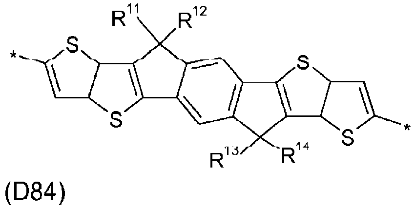


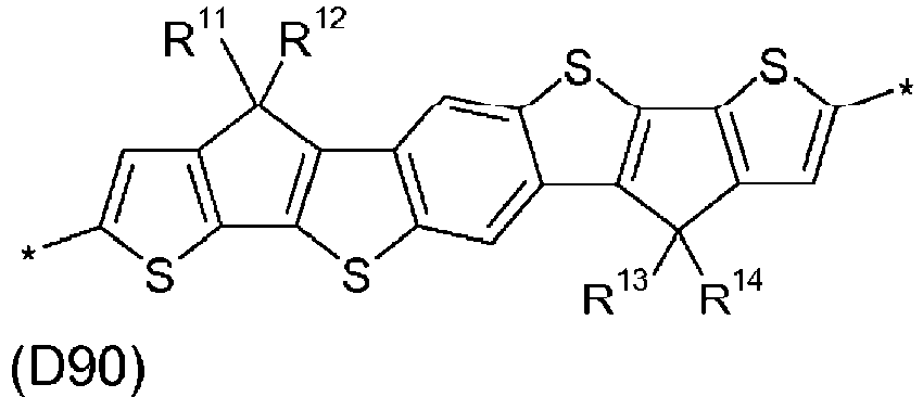


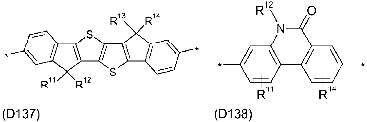


- Polymère selon une ou plusieurs des revendications 1 à 7, dans lequel Ac et/ou Ar3 représente(nt) aryle ou hétéroaryle qui est sélectionné parmi le groupe qui est constitué par les formules qui suivent :


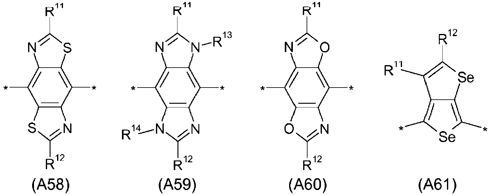


- Polymère selon la revendication 6, caractérisé en ce que les unités de donneur Da, Db, Dc, Dd, De et Df sont sélectionnées parmi les formules qui suivent :





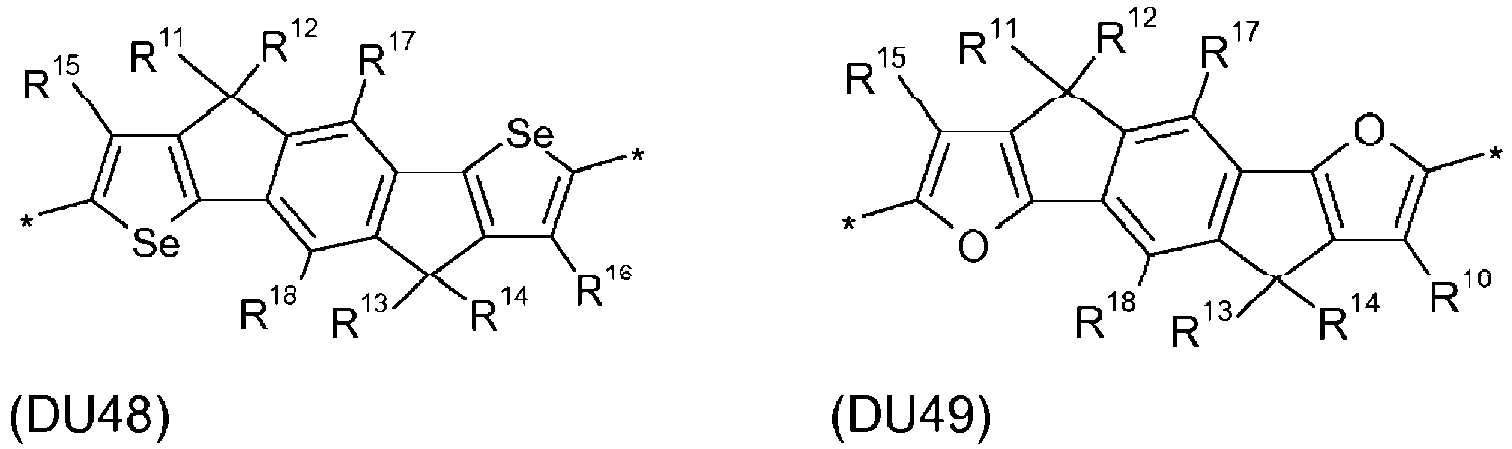


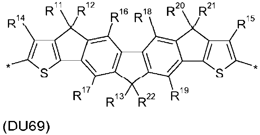


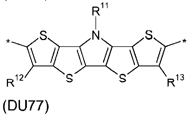
- Polymère selon une ou plusieurs des revendications 1 à 9, caractérisé en ce qu'il est sélectionné parmi la formule V :
R5-chain-R6 V
dans laquelle "chain" est une chaîne polymère qui est sélectionnée parmi les formules IV, IV1 ou IVa-IVk telles qu'elles ont été définies selon la revendication 4, 5 ou 6, R5 et R6 présentent, de manière indépendante l'un de l'autre, l'une des significations de RS telles qu'elles ont été définies selon la revendication 2, ou représentent, de manière indépendante l'un de l'autre, H, F, Br, Cl, I, -CH2Cl, -CHO, -CR'=CR"2, -SiR'R"R"', -SiR'X'X", -SiR'R"X', -SnR'R"R"', -BR'R", -B(OR')(OR"), -B(OH)2, -O-SO2-R', -C≡CH, -C≡C-SiR'3, -ZnX', ou un groupe de coiffe terminale, où X' et X" représentent halogène, R', R" et R'" présentent, de manière indépendante les uns des autres, l'une des significations de R0 qui ont été données selon la revendication 2, et deux de R', R" et R'" peuvent également former un cycle en association avec l'hétéroatome auquel ils sont liés. - Mixture ou mélange de polymères comprenant un ou plusieurs polymère(s) selon une ou plusieurs des revendications 1 à 10 et un ou plusieurs composé(s) ou polymère(s) présentant des propriétés de semiconduction, de transport de charges, de transport de trous/ d'électrons, de blocage de trous/d'électrons, de conduction électrique, de photoconduction ou d'émission de lumière.
- Mixture ou mélange de polymères selon la revendication 11, caractérisé(e) en ce qu'elle/il comprend un ou plusieurs polymère(s) selon une ou plusieurs des revendications 1 à 10 et un ou plusieurs composé(s) semiconducteur(s) organique(s) de type n.
- Mixture ou mélange de polymères selon la revendication 12, caractérisé(e) en ce que le composé semiconducteur organique de type n est un fullerène ou un fullerène substitué.
- Formulation comprenant un ou plusieurs polymère(s), une ou plusieurs mixture(s) ou un ou plusieurs mélange(s) de polymères selon une ou plusieurs des revendications 1 à 13, et un ou plusieurs solvant(s), de préférence sélectionné(s) parmi les solvants organiques.
- Utilisation d'un polymère, d'une mixture, d'un mélange de polymères ou d'une formulation selon une ou plusieurs des revendications 1 à 14 en tant que matériau de transport de charges, de semiconduction, de conduction électrique, de photoconduction ou d'émission de lumière dans un dispositif optique, électrooptique, électronique, électroluminescent ou photoluminescent, ou dans un composant d'un tel dispositif, ou dans un assemblage qui comprend un tel dispositif ou un tel composant.
- Matériau de transport de charges, de semiconduction, de conduction électrique, de photoconduction ou d'émission de lumière qui comprend un polymère, une formulation, une mixture ou un mélange de polymères selon une ou plusieurs des revendications 1 à 15.
- Dispositif optique, électrooptique, électronique, électroluminescent ou photoluminescent, ou un composant de ce dispositif, ou un assemblage qui comprend ce dispositif, lequel comprend un matériau de transport de charges, de semiconduction, de conduction électrique, de photoconduction ou d'émission de lumière, ou comprend un polymère, une mixture, un mélange de polymères ou une formulation selon une ou plusieurs des revendications 1 à 16.
- Dispositif, composant de ce dispositif ou assemblage comprenant ce dispositif selon la revendication 17, dans lequel le dispositif est sélectionné parmi les transistors à effet de champ organiques (OFET), les transistors à film mince (TFT), les diodes à émission de lumière organiques (OLED), les transistors à émission de lumière organiques (OLET), les dispositifs photovoltaïques organiques (OPV), les photodétecteurs organiques (OPD), les cellules laser organiques, les diodes laser, les diodes Schottky et les photoconducteurs, le composant est sélectionné parmi les couches d'injection de charges, les couches de transport de charges, les intercouches, les couches de planarisation, les films antistatiques, les membranes électrolytiques polymère (PEM), les substrats de conduction, les motifs de conduction, et l'assemblage est sélectionné parmi les circuits intégrés (IC), les étiquettes d'identification radiofréquence (RFID) ou les marquages de sécurité ou les dispositifs de sécurité qui les contiennent, les affichages à écran plat ou leurs éclairages arrière ou rétroéclairages, les dispositifs électrophotographiques, les dispositifs d'enregistrement électrophotographique, les dispositifs de mémoire organiques, les dispositifs de capteur, les biocapteurs et les biopuces.
- Dispositif selon la revendication 18, lequel est un OFET, un dispositif OPV à hétérojonction en volume (BHV) ou un dispositif OPV BHJ inversé.
- Monomère de la formule VIa, VIb ou VIc :
R7-(Ar1)a-U-(Ar2)c-R8 VIa
R7-U-(Ar1)a-U-R8 VIb
R7-U-(Da)a1-(Db)b1-(Dc)c1-(Dd)d1-(De)e1-(Df)f1-R8 VIc
dans lesquelles :U, Ar1, Ar2, a et c sont tels qu'ils ont été définis selon la revendication 2 ou 7 ;Da, Db, Dc, Dd, De et Df sont tels qu'ils ont été définis selon la revendication 6 ou 9 ;a1, b1, c1, d1, e1 et f1 sont, de manière indépendante les uns des autres, 0 ou 1, au moins l'un de a1, b1, c1, d1, e1 et f1 étant 1 ; etR7 et R8 sont sélectionnés parmi le groupe qui est constitué par Cl, Br, I, O-tosylate, O-triflate, O-mésylate, O-nonaflate, -SiMe2F, -SiMeF2, -O-SO2Z1, -B(OZ2)2, -CZ3=C(Z3)2, -C≡CH, -C≡CSi(Z1)3, -ZnX0e -Sn(Z4)3, où X0 est halogène, de préférence Cl, Br ou I, Z1-4 sont sélectionnés parmi le groupe qui est constitué par alkyle et aryle, chacun étant en option substitué, et deux groupes Z2 peuvent également former ensemble un groupe cyclique. - Monomère selon la revendication 20, lequel est sélectionné parmi les formules qui suivent :
R7-Ar1-U-Ar2-R8 VI1
R7-U-R8 VI2
R7-Ar1-U-R8 VI3
R7-U-Ar2-R8 VI4
R7-U-Ar1-U-R8 VI5
R7-U-Da-R8 VI6
dans lesquelles U, Da, Ar1, Ar2, R7 et R8 sont tels qu'ils ont été définis selon la revendication 20. - Procédé de préparation d'un polymère selon une ou plusieurs des revendications 1 à 10, par couplage d'un ou de plusieurs monomère(s) selon la revendication 20 ou 21, dans lequel R7 et R8 sont sélectionnés parmi Cl, Br, I, -B(OZ2)2 et -Sn(Z4)3, les uns avec les autres et/ou avec un ou plusieurs monomère(s) qui est/sont sélectionné(s) parmi les formules qui suivent :
R7-(Ar1)a-Ac-(Ar2)c-R8 VIII
R7-Ar1-R8 IX
R7-Ar3-R8 X
R7-Da-R8 XI
dans lesquelles Da, Ar1, Ar2, a et c sont tels qu'ils ont été définis selon la revendication 20, Ar3 est tel qu'il a été défini selon la revendication 2, 7 ou 8, Ac est tel qu'il a été défini selon la revendication 3 ou 8, et R7 et R8 sont sélectionnés parmi Cl, Br, I, -B(OZ2)2 et -Sn(Z4)3, selon une réaction de couplage aryle-aryle.
Priority Applications (1)
| Application Number | Priority Date | Filing Date | Title |
|---|---|---|---|
| EP14777007.7A EP3060622B1 (fr) | 2013-10-22 | 2014-09-26 | Polymères conjugués |
Applications Claiming Priority (3)
| Application Number | Priority Date | Filing Date | Title |
|---|---|---|---|
| EP13005048 | 2013-10-22 | ||
| EP14777007.7A EP3060622B1 (fr) | 2013-10-22 | 2014-09-26 | Polymères conjugués |
| PCT/EP2014/002618 WO2015058827A1 (fr) | 2013-10-22 | 2014-09-26 | Polymères conjugués |
Publications (2)
| Publication Number | Publication Date |
|---|---|
| EP3060622A1 EP3060622A1 (fr) | 2016-08-31 |
| EP3060622B1 true EP3060622B1 (fr) | 2019-06-19 |
Family
ID=49546204
Family Applications (1)
| Application Number | Title | Priority Date | Filing Date |
|---|---|---|---|
| EP14777007.7A Not-in-force EP3060622B1 (fr) | 2013-10-22 | 2014-09-26 | Polymères conjugués |
Country Status (7)
| Country | Link |
|---|---|
| US (1) | US9806263B2 (fr) |
| EP (1) | EP3060622B1 (fr) |
| JP (1) | JP6588429B2 (fr) |
| KR (1) | KR20160076528A (fr) |
| CN (1) | CN105658761B (fr) |
| TW (1) | TWI689526B (fr) |
| WO (1) | WO2015058827A1 (fr) |
Families Citing this family (16)
| Publication number | Priority date | Publication date | Assignee | Title |
|---|---|---|---|---|
| EP2734528B1 (fr) * | 2011-07-19 | 2017-03-29 | Merck Patent GmbH | Semi-conducteurs organiques |
| CN104395372B (zh) * | 2012-07-02 | 2017-04-05 | 默克专利股份有限公司 | 共轭聚合物 |
| KR20160076528A (ko) * | 2013-10-22 | 2016-06-30 | 메르크 파텐트 게엠베하 | 공액 중합체 |
| JP6591417B2 (ja) * | 2013-11-28 | 2019-10-16 | メルク パテント ゲゼルシャフト ミット ベシュレンクテル ハフツングMerck Patent Gesellschaft mit beschraenkter Haftung | チオフェン単位を含む新規の多環式ポリマー、かかるポリマーの製造方法および使用 |
| US10875957B2 (en) * | 2015-11-11 | 2020-12-29 | The Regents Of The University Of California | Fluorine substitution influence on benzo[2,1,3]thiodiazole based polymers for field-effect transistor applications |
| CN106800640B (zh) * | 2015-11-25 | 2019-03-26 | 中国科学院福建物质结构研究所 | 一种聚合物、其制备方法及在太阳能电池中的应用 |
| EP3481832A1 (fr) * | 2016-07-08 | 2019-05-15 | Merck Patent GmbH | Dérivés de dithiénothiophène fusionnés et leur utilisation en tant que semiconducteurs organiques |
| US10707531B1 (en) | 2016-09-27 | 2020-07-07 | New Dominion Enterprises Inc. | All-inorganic solvents for electrolytes |
| US10991893B2 (en) * | 2016-10-05 | 2021-04-27 | Raynergy Tek Incorporation | Organic semiconducting compounds |
| EP3333170B1 (fr) * | 2016-12-06 | 2020-04-29 | Merck Patent GmbH | Composés polycyliques asymmetriques à être utilisés dans des semi-conducteurs organiques |
| WO2018226536A1 (fr) | 2017-06-08 | 2018-12-13 | Corning Incorporated | Dopage d'autres polymères dans des polymères semi-conducteurs organiques |
| GB201810710D0 (en) | 2018-06-29 | 2018-08-15 | Smartkem Ltd | Sputter Protective Layer For Organic Electronic Devices |
| KR102736230B1 (ko) | 2019-05-17 | 2024-11-28 | 삼성전자주식회사 | 광전 변환 소자, 유기 센서 및 전자 장치 |
| GB201919031D0 (en) | 2019-12-20 | 2020-02-05 | Smartkem Ltd | Sputter protective layer for organic electronic devices |
| GB202017982D0 (en) | 2020-11-16 | 2020-12-30 | Smartkem Ltd | Organic thin film transistor |
| GB202209042D0 (en) | 2022-06-20 | 2022-08-10 | Smartkem Ltd | An integrated circuit for a flat-panel display |
Family Cites Families (25)
| Publication number | Priority date | Publication date | Assignee | Title |
|---|---|---|---|---|
| US5892244A (en) | 1989-01-10 | 1999-04-06 | Mitsubishi Denki Kabushiki Kaisha | Field effect transistor including πconjugate polymer and liquid crystal display including the field effect transistor |
| US5198153A (en) | 1989-05-26 | 1993-03-30 | International Business Machines Corporation | Electrically conductive polymeric |
| JP3224829B2 (ja) | 1991-08-15 | 2001-11-05 | 株式会社東芝 | 有機電界効果型素子 |
| WO1996021659A1 (fr) | 1995-01-10 | 1996-07-18 | University Of Technology, Sydney | Semi-conducteur organique |
| US5998804A (en) | 1997-07-03 | 1999-12-07 | Hna Holdings, Inc. | Transistors incorporating substrates comprising liquid crystal polymers |
| EP0889350A1 (fr) | 1997-07-03 | 1999-01-07 | ETHZ Institut für Polymere | Dispositifs d'affichage photoluminescents |
| JP3310658B1 (ja) | 1999-03-05 | 2002-08-05 | ケンブリッジ ディスプレイ テクノロジー リミテッド | 高分子の合成方法 |
| WO2000079617A1 (fr) | 1999-06-21 | 2000-12-28 | Cambridge University Technical Services Limited | Polymeres alignes pour tft organique |
| GB0028867D0 (en) | 2000-11-28 | 2001-01-10 | Avecia Ltd | Field effect translators,methods for the manufacture thereof and materials therefor |
| US20030021913A1 (en) | 2001-07-03 | 2003-01-30 | O'neill Mary | Liquid crystal alignment layer |
| DE10159946A1 (de) | 2001-12-06 | 2003-06-18 | Covion Organic Semiconductors | Prozess zur Herstellung von Aryl-Aryl gekoppelten Verbindungen |
| DE10241814A1 (de) | 2002-09-06 | 2004-03-25 | Covion Organic Semiconductors Gmbh | Prozeß zur Herstellung von Aryl-Aryl gekoppelten Verbindungen |
| DE10337077A1 (de) | 2003-08-12 | 2005-03-10 | Covion Organic Semiconductors | Konjugierte Copolymere, deren Darstellung und Verwendung |
| EP1783781A3 (fr) | 2003-11-28 | 2007-10-03 | Merck Patent GmbH | Améliorations de et associées aux couches de semi-conducteur organique |
| EP2449561A2 (fr) | 2009-06-30 | 2012-05-09 | Plextronics, Inc. | Compositions, procédés et polymères innovants |
| US8691931B2 (en) | 2009-09-04 | 2014-04-08 | Plextronics, Inc. | Organic electronic devices and polymers, including photovoltaic cells and diketone-based and diketopyrrolopyrrole-based polymers |
| US9062152B2 (en) | 2010-09-01 | 2015-06-23 | Solvay Usa, Inc. | Organic electronic devices, including organic photovoltaic devices, polymers, and monomers |
| EP2734528B1 (fr) | 2011-07-19 | 2017-03-29 | Merck Patent GmbH | Semi-conducteurs organiques |
| KR20140135747A (ko) * | 2012-02-15 | 2014-11-26 | 메르크 파텐트 게엠베하 | 공액 중합체 |
| TWI438220B (zh) * | 2012-03-08 | 2014-05-21 | Univ Nat Chiao Tung | 化合物及其合成方法 |
| TWI635111B (zh) * | 2012-03-16 | 2018-09-11 | Merck Patent Gmbh | 共軛聚合物 |
| CN104245787B (zh) * | 2012-04-25 | 2017-02-22 | 默克专利股份有限公司 | 共轭聚合物 |
| CN104245786B (zh) * | 2012-04-25 | 2017-01-25 | 默克专利股份有限公司 | 共轭聚合物 |
| CN104395372B (zh) * | 2012-07-02 | 2017-04-05 | 默克专利股份有限公司 | 共轭聚合物 |
| KR20160076528A (ko) * | 2013-10-22 | 2016-06-30 | 메르크 파텐트 게엠베하 | 공액 중합체 |
-
2014
- 2014-09-26 KR KR1020167013380A patent/KR20160076528A/ko not_active Abandoned
- 2014-09-26 US US15/031,537 patent/US9806263B2/en not_active Expired - Fee Related
- 2014-09-26 CN CN201480057801.XA patent/CN105658761B/zh not_active Expired - Fee Related
- 2014-09-26 EP EP14777007.7A patent/EP3060622B1/fr not_active Not-in-force
- 2014-09-26 WO PCT/EP2014/002618 patent/WO2015058827A1/fr not_active Ceased
- 2014-09-26 JP JP2016525496A patent/JP6588429B2/ja not_active Expired - Fee Related
- 2014-10-21 TW TW103136349A patent/TWI689526B/zh not_active IP Right Cessation
Non-Patent Citations (1)
| Title |
|---|
| None * |
Also Published As
| Publication number | Publication date |
|---|---|
| KR20160076528A (ko) | 2016-06-30 |
| EP3060622A1 (fr) | 2016-08-31 |
| US9806263B2 (en) | 2017-10-31 |
| TWI689526B (zh) | 2020-04-01 |
| US20160276591A1 (en) | 2016-09-22 |
| JP2016538369A (ja) | 2016-12-08 |
| CN105658761A (zh) | 2016-06-08 |
| TW201522410A (zh) | 2015-06-16 |
| WO2015058827A1 (fr) | 2015-04-30 |
| CN105658761B (zh) | 2018-04-24 |
| JP6588429B2 (ja) | 2019-10-09 |
Similar Documents
| Publication | Publication Date | Title |
|---|---|---|
| EP3130016B1 (fr) | Composes semiconducteur organiques | |
| EP3060622B1 (fr) | Polymères conjugués | |
| EP2841484B1 (fr) | Polymères conjugués | |
| EP2734528B1 (fr) | Semi-conducteurs organiques | |
| EP3119776B1 (fr) | Composés semi-conducteurs organiques | |
| US9676901B2 (en) | Conjugated polymers | |
| EP2888307B1 (fr) | Polymères conjugués | |
| US9695190B2 (en) | Conjugated polymers | |
| EP2611851B1 (fr) | Polymères conjugués | |
| EP3074451B1 (fr) | Nouveau polymère polycyclique comprenant des motifs thiophène, son procédé de production et ses utilisations | |
| EP3194480B1 (fr) | Polymères conjugués | |
| EP2814863B1 (fr) | Polymères conjugués | |
| EP2814861B1 (fr) | Polymères semi-conducteurs organiques | |
| WO2013182262A1 (fr) | Semi-conducteurs organiques | |
| EP3411374B9 (fr) | Composés [1,5]-naphthyridine et polymères utilisés comme semi-conducteurs | |
| EP2760909B1 (fr) | Polymères conjugués | |
| US20140346407A1 (en) | Conjugated Polymers | |
| US20150333263A1 (en) | Polymer comprising a naphthalene group and its use in organic electronic devices | |
| EP2935427B1 (fr) | Polymère comprenant un groupe thiadiazol, production d'un tel polymère et son utilisation dans des dispositifs électroniques organiques | |
| EP3149107B1 (fr) | Polymères polycycliques à base de tétra-aryl indacenodithiophène et leur utilisation | |
| EP2935235B1 (fr) | Composés à base d'indénophénanthrène | |
| EP3430654B1 (fr) | Semi-conducteurs organiques |
Legal Events
| Date | Code | Title | Description |
|---|---|---|---|
| PUAI | Public reference made under article 153(3) epc to a published international application that has entered the european phase |
Free format text: ORIGINAL CODE: 0009012 |
|
| 17P | Request for examination filed |
Effective date: 20160304 |
|
| AK | Designated contracting states |
Kind code of ref document: A1 Designated state(s): AL AT BE BG CH CY CZ DE DK EE ES FI FR GB GR HR HU IE IS IT LI LT LU LV MC MK MT NL NO PL PT RO RS SE SI SK SM TR |
|
| AX | Request for extension of the european patent |
Extension state: BA ME |
|
| DAX | Request for extension of the european patent (deleted) | ||
| STAA | Information on the status of an ep patent application or granted ep patent |
Free format text: STATUS: EXAMINATION IS IN PROGRESS |
|
| 17Q | First examination report despatched |
Effective date: 20180112 |
|
| GRAP | Despatch of communication of intention to grant a patent |
Free format text: ORIGINAL CODE: EPIDOSNIGR1 |
|
| STAA | Information on the status of an ep patent application or granted ep patent |
Free format text: STATUS: GRANT OF PATENT IS INTENDED |
|
| INTG | Intention to grant announced |
Effective date: 20190226 |
|
| GRAS | Grant fee paid |
Free format text: ORIGINAL CODE: EPIDOSNIGR3 |
|
| GRAA | (expected) grant |
Free format text: ORIGINAL CODE: 0009210 |
|
| STAA | Information on the status of an ep patent application or granted ep patent |
Free format text: STATUS: THE PATENT HAS BEEN GRANTED |
|
| AK | Designated contracting states |
Kind code of ref document: B1 Designated state(s): AL AT BE BG CH CY CZ DE DK EE ES FI FR GB GR HR HU IE IS IT LI LT LU LV MC MK MT NL NO PL PT RO RS SE SI SK SM TR |
|
| REG | Reference to a national code |
Ref country code: GB Ref legal event code: FG4D |
|
| REG | Reference to a national code |
Ref country code: CH Ref legal event code: EP |
|
| REG | Reference to a national code |
Ref country code: IE Ref legal event code: FG4D |
|
| REG | Reference to a national code |
Ref country code: DE Ref legal event code: R096 Ref document number: 602014048699 Country of ref document: DE |
|
| REG | Reference to a national code |
Ref country code: AT Ref legal event code: REF Ref document number: 1145494 Country of ref document: AT Kind code of ref document: T Effective date: 20190715 |
|
| REG | Reference to a national code |
Ref country code: NL Ref legal event code: MP Effective date: 20190619 |
|
| PG25 | Lapsed in a contracting state [announced via postgrant information from national office to epo] |
Ref country code: HR Free format text: LAPSE BECAUSE OF FAILURE TO SUBMIT A TRANSLATION OF THE DESCRIPTION OR TO PAY THE FEE WITHIN THE PRESCRIBED TIME-LIMIT Effective date: 20190619 Ref country code: FI Free format text: LAPSE BECAUSE OF FAILURE TO SUBMIT A TRANSLATION OF THE DESCRIPTION OR TO PAY THE FEE WITHIN THE PRESCRIBED TIME-LIMIT Effective date: 20190619 Ref country code: LT Free format text: LAPSE BECAUSE OF FAILURE TO SUBMIT A TRANSLATION OF THE DESCRIPTION OR TO PAY THE FEE WITHIN THE PRESCRIBED TIME-LIMIT Effective date: 20190619 Ref country code: SE Free format text: LAPSE BECAUSE OF FAILURE TO SUBMIT A TRANSLATION OF THE DESCRIPTION OR TO PAY THE FEE WITHIN THE PRESCRIBED TIME-LIMIT Effective date: 20190619 Ref country code: NO Free format text: LAPSE BECAUSE OF FAILURE TO SUBMIT A TRANSLATION OF THE DESCRIPTION OR TO PAY THE FEE WITHIN THE PRESCRIBED TIME-LIMIT Effective date: 20190919 Ref country code: AL Free format text: LAPSE BECAUSE OF FAILURE TO SUBMIT A TRANSLATION OF THE DESCRIPTION OR TO PAY THE FEE WITHIN THE PRESCRIBED TIME-LIMIT Effective date: 20190619 |
|
| REG | Reference to a national code |
Ref country code: LT Ref legal event code: MG4D |
|
| PG25 | Lapsed in a contracting state [announced via postgrant information from national office to epo] |
Ref country code: GR Free format text: LAPSE BECAUSE OF FAILURE TO SUBMIT A TRANSLATION OF THE DESCRIPTION OR TO PAY THE FEE WITHIN THE PRESCRIBED TIME-LIMIT Effective date: 20190920 Ref country code: BG Free format text: LAPSE BECAUSE OF FAILURE TO SUBMIT A TRANSLATION OF THE DESCRIPTION OR TO PAY THE FEE WITHIN THE PRESCRIBED TIME-LIMIT Effective date: 20190919 Ref country code: RS Free format text: LAPSE BECAUSE OF FAILURE TO SUBMIT A TRANSLATION OF THE DESCRIPTION OR TO PAY THE FEE WITHIN THE PRESCRIBED TIME-LIMIT Effective date: 20190619 Ref country code: LV Free format text: LAPSE BECAUSE OF FAILURE TO SUBMIT A TRANSLATION OF THE DESCRIPTION OR TO PAY THE FEE WITHIN THE PRESCRIBED TIME-LIMIT Effective date: 20190619 |
|
| REG | Reference to a national code |
Ref country code: AT Ref legal event code: MK05 Ref document number: 1145494 Country of ref document: AT Kind code of ref document: T Effective date: 20190619 |
|
| PG25 | Lapsed in a contracting state [announced via postgrant information from national office to epo] |
Ref country code: EE Free format text: LAPSE BECAUSE OF FAILURE TO SUBMIT A TRANSLATION OF THE DESCRIPTION OR TO PAY THE FEE WITHIN THE PRESCRIBED TIME-LIMIT Effective date: 20190619 Ref country code: SK Free format text: LAPSE BECAUSE OF FAILURE TO SUBMIT A TRANSLATION OF THE DESCRIPTION OR TO PAY THE FEE WITHIN THE PRESCRIBED TIME-LIMIT Effective date: 20190619 Ref country code: AT Free format text: LAPSE BECAUSE OF FAILURE TO SUBMIT A TRANSLATION OF THE DESCRIPTION OR TO PAY THE FEE WITHIN THE PRESCRIBED TIME-LIMIT Effective date: 20190619 Ref country code: PT Free format text: LAPSE BECAUSE OF FAILURE TO SUBMIT A TRANSLATION OF THE DESCRIPTION OR TO PAY THE FEE WITHIN THE PRESCRIBED TIME-LIMIT Effective date: 20191021 Ref country code: NL Free format text: LAPSE BECAUSE OF FAILURE TO SUBMIT A TRANSLATION OF THE DESCRIPTION OR TO PAY THE FEE WITHIN THE PRESCRIBED TIME-LIMIT Effective date: 20190619 Ref country code: CZ Free format text: LAPSE BECAUSE OF FAILURE TO SUBMIT A TRANSLATION OF THE DESCRIPTION OR TO PAY THE FEE WITHIN THE PRESCRIBED TIME-LIMIT Effective date: 20190619 Ref country code: RO Free format text: LAPSE BECAUSE OF FAILURE TO SUBMIT A TRANSLATION OF THE DESCRIPTION OR TO PAY THE FEE WITHIN THE PRESCRIBED TIME-LIMIT Effective date: 20190619 |
|
| PG25 | Lapsed in a contracting state [announced via postgrant information from national office to epo] |
Ref country code: SM Free format text: LAPSE BECAUSE OF FAILURE TO SUBMIT A TRANSLATION OF THE DESCRIPTION OR TO PAY THE FEE WITHIN THE PRESCRIBED TIME-LIMIT Effective date: 20190619 Ref country code: ES Free format text: LAPSE BECAUSE OF FAILURE TO SUBMIT A TRANSLATION OF THE DESCRIPTION OR TO PAY THE FEE WITHIN THE PRESCRIBED TIME-LIMIT Effective date: 20190619 Ref country code: IT Free format text: LAPSE BECAUSE OF FAILURE TO SUBMIT A TRANSLATION OF THE DESCRIPTION OR TO PAY THE FEE WITHIN THE PRESCRIBED TIME-LIMIT Effective date: 20190619 Ref country code: IS Free format text: LAPSE BECAUSE OF FAILURE TO SUBMIT A TRANSLATION OF THE DESCRIPTION OR TO PAY THE FEE WITHIN THE PRESCRIBED TIME-LIMIT Effective date: 20191019 |
|
| PG25 | Lapsed in a contracting state [announced via postgrant information from national office to epo] |
Ref country code: TR Free format text: LAPSE BECAUSE OF FAILURE TO SUBMIT A TRANSLATION OF THE DESCRIPTION OR TO PAY THE FEE WITHIN THE PRESCRIBED TIME-LIMIT Effective date: 20190619 |
|
| REG | Reference to a national code |
Ref country code: DE Ref legal event code: R119 Ref document number: 602014048699 Country of ref document: DE |
|
| REG | Reference to a national code |
Ref country code: GB Ref legal event code: 732E Free format text: REGISTERED BETWEEN 20200312 AND 20200318 |
|
| PG25 | Lapsed in a contracting state [announced via postgrant information from national office to epo] |
Ref country code: PL Free format text: LAPSE BECAUSE OF FAILURE TO SUBMIT A TRANSLATION OF THE DESCRIPTION OR TO PAY THE FEE WITHIN THE PRESCRIBED TIME-LIMIT Effective date: 20190619 Ref country code: DK Free format text: LAPSE BECAUSE OF FAILURE TO SUBMIT A TRANSLATION OF THE DESCRIPTION OR TO PAY THE FEE WITHIN THE PRESCRIBED TIME-LIMIT Effective date: 20190619 |
|
| RAP2 | Party data changed (patent owner data changed or rights of a patent transferred) |
Owner name: FLEXENABLE LIMITED |
|
| PG25 | Lapsed in a contracting state [announced via postgrant information from national office to epo] |
Ref country code: IS Free format text: LAPSE BECAUSE OF FAILURE TO SUBMIT A TRANSLATION OF THE DESCRIPTION OR TO PAY THE FEE WITHIN THE PRESCRIBED TIME-LIMIT Effective date: 20200224 Ref country code: MC Free format text: LAPSE BECAUSE OF FAILURE TO SUBMIT A TRANSLATION OF THE DESCRIPTION OR TO PAY THE FEE WITHIN THE PRESCRIBED TIME-LIMIT Effective date: 20190619 |
|
| REG | Reference to a national code |
Ref country code: CH Ref legal event code: PL |
|
| PLBE | No opposition filed within time limit |
Free format text: ORIGINAL CODE: 0009261 |
|
| STAA | Information on the status of an ep patent application or granted ep patent |
Free format text: STATUS: NO OPPOSITION FILED WITHIN TIME LIMIT |
|
| PG2D | Information on lapse in contracting state deleted |
Ref country code: IS |
|
| PG25 | Lapsed in a contracting state [announced via postgrant information from national office to epo] |
Ref country code: LU Free format text: LAPSE BECAUSE OF NON-PAYMENT OF DUE FEES Effective date: 20190926 Ref country code: DE Free format text: LAPSE BECAUSE OF NON-PAYMENT OF DUE FEES Effective date: 20200401 Ref country code: CH Free format text: LAPSE BECAUSE OF NON-PAYMENT OF DUE FEES Effective date: 20190930 Ref country code: IE Free format text: LAPSE BECAUSE OF NON-PAYMENT OF DUE FEES Effective date: 20190926 Ref country code: LI Free format text: LAPSE BECAUSE OF NON-PAYMENT OF DUE FEES Effective date: 20190930 |
|
| REG | Reference to a national code |
Ref country code: BE Ref legal event code: MM Effective date: 20190930 |
|
| 26N | No opposition filed |
Effective date: 20200603 |
|
| PG25 | Lapsed in a contracting state [announced via postgrant information from national office to epo] |
Ref country code: SI Free format text: LAPSE BECAUSE OF FAILURE TO SUBMIT A TRANSLATION OF THE DESCRIPTION OR TO PAY THE FEE WITHIN THE PRESCRIBED TIME-LIMIT Effective date: 20190619 Ref country code: BE Free format text: LAPSE BECAUSE OF NON-PAYMENT OF DUE FEES Effective date: 20190930 |
|
| PG25 | Lapsed in a contracting state [announced via postgrant information from national office to epo] |
Ref country code: FR Free format text: LAPSE BECAUSE OF NON-PAYMENT OF DUE FEES Effective date: 20190930 |
|
| PGFP | Annual fee paid to national office [announced via postgrant information from national office to epo] |
Ref country code: GB Payment date: 20200916 Year of fee payment: 7 |
|
| PG25 | Lapsed in a contracting state [announced via postgrant information from national office to epo] |
Ref country code: CY Free format text: LAPSE BECAUSE OF FAILURE TO SUBMIT A TRANSLATION OF THE DESCRIPTION OR TO PAY THE FEE WITHIN THE PRESCRIBED TIME-LIMIT Effective date: 20190619 |
|
| PG25 | Lapsed in a contracting state [announced via postgrant information from national office to epo] |
Ref country code: HU Free format text: LAPSE BECAUSE OF FAILURE TO SUBMIT A TRANSLATION OF THE DESCRIPTION OR TO PAY THE FEE WITHIN THE PRESCRIBED TIME-LIMIT; INVALID AB INITIO Effective date: 20140926 Ref country code: MT Free format text: LAPSE BECAUSE OF FAILURE TO SUBMIT A TRANSLATION OF THE DESCRIPTION OR TO PAY THE FEE WITHIN THE PRESCRIBED TIME-LIMIT Effective date: 20190619 |
|
| GBPC | Gb: european patent ceased through non-payment of renewal fee |
Effective date: 20210926 |
|
| PG25 | Lapsed in a contracting state [announced via postgrant information from national office to epo] |
Ref country code: MK Free format text: LAPSE BECAUSE OF FAILURE TO SUBMIT A TRANSLATION OF THE DESCRIPTION OR TO PAY THE FEE WITHIN THE PRESCRIBED TIME-LIMIT Effective date: 20190619 |
|
| PG25 | Lapsed in a contracting state [announced via postgrant information from national office to epo] |
Ref country code: GB Free format text: LAPSE BECAUSE OF NON-PAYMENT OF DUE FEES Effective date: 20210926 |
|
| P01 | Opt-out of the competence of the unified patent court (upc) registered |
Effective date: 20230528 |