EP3065187A1 - Wellenlängenumwandlungsmaterialanordnung - Google Patents
Wellenlängenumwandlungsmaterialanordnung Download PDFInfo
- Publication number
- EP3065187A1 EP3065187A1 EP16155480.3A EP16155480A EP3065187A1 EP 3065187 A1 EP3065187 A1 EP 3065187A1 EP 16155480 A EP16155480 A EP 16155480A EP 3065187 A1 EP3065187 A1 EP 3065187A1
- Authority
- EP
- European Patent Office
- Prior art keywords
- spots
- light
- wavelength conversion
- lenslets
- conversion material
- Prior art date
- Legal status (The legal status is an assumption and is not a legal conclusion. Google has not performed a legal analysis and makes no representation as to the accuracy of the status listed.)
- Granted
Links
- 238000006243 chemical reaction Methods 0.000 title claims abstract description 110
- 239000000463 material Substances 0.000 title claims abstract description 84
- 230000005284 excitation Effects 0.000 claims abstract description 72
- 230000003287 optical effect Effects 0.000 claims description 25
- OAICVXFJPJFONN-UHFFFAOYSA-N Phosphorus Chemical compound [P] OAICVXFJPJFONN-UHFFFAOYSA-N 0.000 claims description 5
- 239000002096 quantum dot Substances 0.000 claims description 4
- 230000006870 function Effects 0.000 description 13
- 230000004907 flux Effects 0.000 description 11
- 230000007423 decrease Effects 0.000 description 7
- 238000003491 array Methods 0.000 description 4
- 230000008901 benefit Effects 0.000 description 3
- 238000000034 method Methods 0.000 description 3
- 230000008569 process Effects 0.000 description 2
- 229910000831 Steel Inorganic materials 0.000 description 1
- 229910052782 aluminium Inorganic materials 0.000 description 1
- XAGFODPZIPBFFR-UHFFFAOYSA-N aluminium Chemical compound [Al] XAGFODPZIPBFFR-UHFFFAOYSA-N 0.000 description 1
- 238000013459 approach Methods 0.000 description 1
- 238000001816 cooling Methods 0.000 description 1
- 230000001419 dependent effect Effects 0.000 description 1
- 230000003292 diminished effect Effects 0.000 description 1
- 230000000694 effects Effects 0.000 description 1
- 238000001125 extrusion Methods 0.000 description 1
- 238000010438 heat treatment Methods 0.000 description 1
- 238000005286 illumination Methods 0.000 description 1
- 238000004519 manufacturing process Methods 0.000 description 1
- 229910052751 metal Inorganic materials 0.000 description 1
- 239000002184 metal Substances 0.000 description 1
- 238000012986 modification Methods 0.000 description 1
- 230000004048 modification Effects 0.000 description 1
- 230000005855 radiation Effects 0.000 description 1
- 238000000926 separation method Methods 0.000 description 1
- 239000010959 steel Substances 0.000 description 1
- 230000003685 thermal hair damage Effects 0.000 description 1
Images


Classifications
-
- G—PHYSICS
- G03—PHOTOGRAPHY; CINEMATOGRAPHY; ANALOGOUS TECHNIQUES USING WAVES OTHER THAN OPTICAL WAVES; ELECTROGRAPHY; HOLOGRAPHY
- G03B—APPARATUS OR ARRANGEMENTS FOR TAKING PHOTOGRAPHS OR FOR PROJECTING OR VIEWING THEM; APPARATUS OR ARRANGEMENTS EMPLOYING ANALOGOUS TECHNIQUES USING WAVES OTHER THAN OPTICAL WAVES; ACCESSORIES THEREFOR
- G03B21/00—Projectors or projection-type viewers; Accessories therefor
- G03B21/14—Details
- G03B21/20—Lamp housings
- G03B21/2006—Lamp housings characterised by the light source
- G03B21/2033—LED or laser light sources
- G03B21/204—LED or laser light sources using secondary light emission, e.g. luminescence or fluorescence
-
- F—MECHANICAL ENGINEERING; LIGHTING; HEATING; WEAPONS; BLASTING
- F21—LIGHTING
- F21V—FUNCTIONAL FEATURES OR DETAILS OF LIGHTING DEVICES OR SYSTEMS THEREOF; STRUCTURAL COMBINATIONS OF LIGHTING DEVICES WITH OTHER ARTICLES, NOT OTHERWISE PROVIDED FOR
- F21V5/00—Refractors for light sources
- F21V5/008—Combination of two or more successive refractors along an optical axis
-
- F—MECHANICAL ENGINEERING; LIGHTING; HEATING; WEAPONS; BLASTING
- F21—LIGHTING
- F21V—FUNCTIONAL FEATURES OR DETAILS OF LIGHTING DEVICES OR SYSTEMS THEREOF; STRUCTURAL COMBINATIONS OF LIGHTING DEVICES WITH OTHER ARTICLES, NOT OTHERWISE PROVIDED FOR
- F21V13/00—Producing particular characteristics or distribution of the light emitted by means of a combination of elements specified in two or more of main groups F21V1/00 - F21V11/00
- F21V13/02—Combinations of only two kinds of elements
- F21V13/04—Combinations of only two kinds of elements the elements being reflectors and refractors
-
- F—MECHANICAL ENGINEERING; LIGHTING; HEATING; WEAPONS; BLASTING
- F21—LIGHTING
- F21V—FUNCTIONAL FEATURES OR DETAILS OF LIGHTING DEVICES OR SYSTEMS THEREOF; STRUCTURAL COMBINATIONS OF LIGHTING DEVICES WITH OTHER ARTICLES, NOT OTHERWISE PROVIDED FOR
- F21V13/00—Producing particular characteristics or distribution of the light emitted by means of a combination of elements specified in two or more of main groups F21V1/00 - F21V11/00
- F21V13/12—Combinations of only three kinds of elements
- F21V13/14—Combinations of only three kinds of elements the elements being filters or photoluminescent elements, reflectors and refractors
-
- F—MECHANICAL ENGINEERING; LIGHTING; HEATING; WEAPONS; BLASTING
- F21—LIGHTING
- F21V—FUNCTIONAL FEATURES OR DETAILS OF LIGHTING DEVICES OR SYSTEMS THEREOF; STRUCTURAL COMBINATIONS OF LIGHTING DEVICES WITH OTHER ARTICLES, NOT OTHERWISE PROVIDED FOR
- F21V29/00—Protecting lighting devices from thermal damage; Cooling or heating arrangements specially adapted for lighting devices or systems
- F21V29/50—Cooling arrangements
- F21V29/502—Cooling arrangements characterised by the adaptation for cooling of specific components
-
- F—MECHANICAL ENGINEERING; LIGHTING; HEATING; WEAPONS; BLASTING
- F21—LIGHTING
- F21V—FUNCTIONAL FEATURES OR DETAILS OF LIGHTING DEVICES OR SYSTEMS THEREOF; STRUCTURAL COMBINATIONS OF LIGHTING DEVICES WITH OTHER ARTICLES, NOT OTHERWISE PROVIDED FOR
- F21V29/00—Protecting lighting devices from thermal damage; Cooling or heating arrangements specially adapted for lighting devices or systems
- F21V29/50—Cooling arrangements
- F21V29/70—Cooling arrangements characterised by passive heat-dissipating elements, e.g. heat-sinks
-
- F—MECHANICAL ENGINEERING; LIGHTING; HEATING; WEAPONS; BLASTING
- F21—LIGHTING
- F21V—FUNCTIONAL FEATURES OR DETAILS OF LIGHTING DEVICES OR SYSTEMS THEREOF; STRUCTURAL COMBINATIONS OF LIGHTING DEVICES WITH OTHER ARTICLES, NOT OTHERWISE PROVIDED FOR
- F21V5/00—Refractors for light sources
- F21V5/007—Array of lenses or refractors for a cluster of light sources, e.g. for arrangement of multiple light sources in one plane
-
- F—MECHANICAL ENGINEERING; LIGHTING; HEATING; WEAPONS; BLASTING
- F21—LIGHTING
- F21V—FUNCTIONAL FEATURES OR DETAILS OF LIGHTING DEVICES OR SYSTEMS THEREOF; STRUCTURAL COMBINATIONS OF LIGHTING DEVICES WITH OTHER ARTICLES, NOT OTHERWISE PROVIDED FOR
- F21V7/00—Reflectors for light sources
- F21V7/0008—Reflectors for light sources providing for indirect lighting
-
- F—MECHANICAL ENGINEERING; LIGHTING; HEATING; WEAPONS; BLASTING
- F21—LIGHTING
- F21V—FUNCTIONAL FEATURES OR DETAILS OF LIGHTING DEVICES OR SYSTEMS THEREOF; STRUCTURAL COMBINATIONS OF LIGHTING DEVICES WITH OTHER ARTICLES, NOT OTHERWISE PROVIDED FOR
- F21V9/00—Elements for modifying spectral properties, polarisation or intensity of the light emitted, e.g. filters
- F21V9/30—Elements containing photoluminescent material distinct from or spaced from the light source
- F21V9/32—Elements containing photoluminescent material distinct from or spaced from the light source characterised by the arrangement of the photoluminescent material
-
- G—PHYSICS
- G03—PHOTOGRAPHY; CINEMATOGRAPHY; ANALOGOUS TECHNIQUES USING WAVES OTHER THAN OPTICAL WAVES; ELECTROGRAPHY; HOLOGRAPHY
- G03B—APPARATUS OR ARRANGEMENTS FOR TAKING PHOTOGRAPHS OR FOR PROJECTING OR VIEWING THEM; APPARATUS OR ARRANGEMENTS EMPLOYING ANALOGOUS TECHNIQUES USING WAVES OTHER THAN OPTICAL WAVES; ACCESSORIES THEREFOR
- G03B21/00—Projectors or projection-type viewers; Accessories therefor
- G03B21/14—Details
- G03B21/16—Cooling; Preventing overheating
-
- H—ELECTRICITY
- H10—SEMICONDUCTOR DEVICES; ELECTRIC SOLID-STATE DEVICES NOT OTHERWISE PROVIDED FOR
- H10H—INORGANIC LIGHT-EMITTING SEMICONDUCTOR DEVICES HAVING POTENTIAL BARRIERS
- H10H20/00—Individual inorganic light-emitting semiconductor devices having potential barriers, e.g. light-emitting diodes [LED]
- H10H20/80—Constructional details
- H10H20/85—Packages
- H10H20/851—Wavelength conversion means
- H10H20/8516—Wavelength conversion means having a non-uniform spatial arrangement or non-uniform concentration, e.g. patterned wavelength conversion layer or wavelength conversion layer with a concentration gradient
-
- H—ELECTRICITY
- H10—SEMICONDUCTOR DEVICES; ELECTRIC SOLID-STATE DEVICES NOT OTHERWISE PROVIDED FOR
- H10H—INORGANIC LIGHT-EMITTING SEMICONDUCTOR DEVICES HAVING POTENTIAL BARRIERS
- H10H20/00—Individual inorganic light-emitting semiconductor devices having potential barriers, e.g. light-emitting diodes [LED]
- H10H20/80—Constructional details
- H10H20/85—Packages
- H10H20/855—Optical field-shaping means, e.g. lenses
-
- H—ELECTRICITY
- H01—ELECTRIC ELEMENTS
- H01S—DEVICES USING THE PROCESS OF LIGHT AMPLIFICATION BY STIMULATED EMISSION OF RADIATION [LASER] TO AMPLIFY OR GENERATE LIGHT; DEVICES USING STIMULATED EMISSION OF ELECTROMAGNETIC RADIATION IN WAVE RANGES OTHER THAN OPTICAL
- H01S5/00—Semiconductor lasers
- H01S5/005—Optical components external to the laser cavity, specially adapted therefor, e.g. for homogenisation or merging of the beams or for manipulating laser pulses, e.g. pulse shaping
- H01S5/0071—Optical components external to the laser cavity, specially adapted therefor, e.g. for homogenisation or merging of the beams or for manipulating laser pulses, e.g. pulse shaping for beam steering, e.g. using a mirror outside the cavity to change the beam direction
-
- H—ELECTRICITY
- H01—ELECTRIC ELEMENTS
- H01S—DEVICES USING THE PROCESS OF LIGHT AMPLIFICATION BY STIMULATED EMISSION OF RADIATION [LASER] TO AMPLIFY OR GENERATE LIGHT; DEVICES USING STIMULATED EMISSION OF ELECTROMAGNETIC RADIATION IN WAVE RANGES OTHER THAN OPTICAL
- H01S5/00—Semiconductor lasers
- H01S5/005—Optical components external to the laser cavity, specially adapted therefor, e.g. for homogenisation or merging of the beams or for manipulating laser pulses, e.g. pulse shaping
- H01S5/0087—Optical components external to the laser cavity, specially adapted therefor, e.g. for homogenisation or merging of the beams or for manipulating laser pulses, e.g. pulse shaping for illuminating phosphorescent or fluorescent materials, e.g. using optical arrangements specifically adapted for guiding or shaping laser beams illuminating these materials
Definitions
- the specification relates generally to display systems, and specifically to a system that includes a wavelength conversion material array.
- a limiting factor in the performance of laser-phosphor illumination systems can be a high energy density of the illuminated spot, as compared to non-laser systems, and an ability (or rather an inability) to remove heat energy from the spot before thermal damage occurs.
- Numerous methods have been used to distribute the thermal energy, for example by rotating or translating the phosphor or illuminated spot, or by increasing the spot size and therefore reducing the energy density.
- these approaches can result in an increase in system complexity and/or in diminished optical performance.
- this disclosure is directed to a system that includes a wavelength conversion material on a heatsink, the wavelength conversion material having a relative area of unity, but divided into an array of 4 to 12 spots.
- a distance between the spots is selected to balance optical collection efficiency with heat flow in the system.
- a lenslet array is used to distribute excitation light from an excitation light source, such as a laser, to each of the spots in the array, and then collect light emitted from the spots.
- the array of spots replaces a single spot of wavelength conversion material of the prior art: a combined relative area of unity of the spots equals a relative area of unity of one larger original spot (the combined area not including spaces between the spots).
- the energy density in the wavelength conversion material remains unchanged, however by separating the wavelength conversion material into an array of smaller spots, the heatsink effectiveness can be improved and therefore the phosphor can be more effectively cooled as compared to systems with one large spot of wavelength conversion material.
- This can permit higher energy levels incident to the wavelength conversion material (e.g. including, but not limited to, phosphors) and hence can therefore generate more light.
- Such factors can be independent of the number of spots, however it is assumed that the number of spots is greater than or equal to three.
- elements may be described as “configured to” perform one or more functions or “configured for” such functions.
- an element that is configured to perform or configured for performing a function is enabled to perform the function, or is suitable for performing the function, or is adapted to perform the function, or is operable to perform the function, or is otherwise capable of performing the function.
- An aspect of the specification provides a system comprising: a light source configured to emit excitation light at an excitation wavelength; a heatsink; a wavelength conversion material located on the heatsink, the wavelength conversion material comprising a relative wavelength conversion area of unity divided into an array of spots, a number of the spots in a range of 4 to 12, the wavelength conversion material configured to emit light at a wavelength greater than the excitation wavelength when irradiated by the excitation light; and, an array of lenslets configured to: receive the excitation light from the light source and irradiate each of the spots of the wavelength conversion material with the excitation light, the lenslets in a one-to-one relationship with the number of spots; and collect the light emitted by the wavelength conversion material.
- a distance between a light emitting surface of the spots and a light receiving surface of the lenslets, and a centre-to-centre distance between the spots can be selected so that lenslets collect light up to an emission angle ⁇ of about 75° as measured from a normal of the spots.
- a distance h between a light emitting surface of the spots and a light receiving surface of the lenslets can be selected so that the lenslets collect light up to an emission angle of about 75° from the spots as measured from a normal of the spots.
- An absolute wavelength conversion area of the array of spots can be in a range of about 2 mm 2 to about 100 mm 2 .
- An absolute wavelength conversion area of the array of spots can be in a range of about 4 mm 2 to about 20 mm 2 .
- the array of lenslets can comprise a collimating lens array.
- the array of lenslets can comprise an integrated lens array.
- the system can further comprise a mirror configured to: reflect the excitation light from the light source towards the array of lenslets; and, transmit the light emitted by the wavelength conversion material that is collected by the lenslets.
- the excitation light can comprise blue light.
- the light emitted by the wavelength conversion material can comprise one or more of green light and red light.
- the heatsink can comprise a thermal conductivity in a range of about 50 to about 600 W/mK.
- the light source can comprise a laser.
- the light source can further comprise one or more optical devices configured to shape the excitation light to an area of the array of lenslets.
- the wavelength conversion material can comprise a phosphor.
- the wavelength conversion material can comprise quantum dots.
- the heatsink can be stationary.
- the heatsink can be configured to rotate.
- the present specification also provides a system comprising: a light source configured to emit excitation light at an excitation wavelength; a heatsink; a wavelength conversion material located on the heatsink, the wavelength conversion material comprising a relative wavelength conversion area of unity divided into an array of spots, wherein, one or more of 5d ⁇ t ⁇ 25d and 10d ⁇ t ⁇ 20d, where d is a centre-to-centre distance between the spots and t is a largest lateral dimension of the spots, is used to select the centre-to-centre distance between the spots; and, an array of lenslets configured to: receive the excitation light from the light source and irradiate each of the spots of the wavelength conversion material with the excitation light, the lenslets in a one-to-one relationship with the number of spots; and collect the light emitted by the wavelength conversion material.
- a number of the spots can be one or more of: greater than or equal to three; in a range of three to twenty, inclusive; and in a range of four to sixteen, inclusive.
- a system comprising: a light source configured to emit excitation light at an excitation wavelength; a heatsink; a wavelength conversion material located on the heatsink, the wavelength conversion material comprising a relative wavelength conversion area of unity divided into an array of spots,; and, an array of lenslets configured to: receive the excitation light from the light source and irradiate each of the spots of the wavelength conversion material with the excitation light, the lenslets in a one-to-one relationship with the number of spots; and collect the light emitted by the wavelength conversion material, wherein a distance between a light emitting surface of the spots and a light receiving surface of the lenslets, and a centre-to-centre distance between the spots is selected so that lenslets collect light up to an emission angle ⁇ of about 75° as measured from a normal of the spots.
- a number of the spots can be one or more of: greater than or equal to three; in a range of three to twenty, inclusive; and in a range of four to sixteen, inclusive.
- Figs. 1 and 2 each depicts a side view of a system 100 comprising: a light source 101 configured to emit excitation light 103 at an excitation wavelength; a heatsink 105 (depicted in cross-section); a wavelength conversion material located on heatsink 105, wavelength conversion material comprising a relative wavelength conversion area of unity divided into an array of spots 107, a number of the spots in a range of 4 to 12, the wavelength conversion material configured to emit light at a wavelength greater than the excitation wavelength when irradiated by excitation light 103; an array of lenslets 109 configured to: receive excitation light 103 from light source 101 and irradiate each of spots 107 of the wavelength conversion material with excitation light 103, lenslets 109 in a one-to-one relationship with the number of spots 107; and collect light 203 emitted by the wavelength conversion material.
- Fig. 1 depicts spots 107 being irradiated with excitation light 103
- Fig. 2 depicts spots 107 emitting light 203; while these two processes are depicted separately, it is appreciated they occur simultaneously and/or in tandem.
- spots 107 are irradiated with excitation light 103
- spots 107 emit light 203.
- ranges provided herein are inclusive of the beginning and end numbers unless otherwise explicitly stated.
- a number of spots in range of 4 to 12 includes: 4 spots, 5 spots, 6 spots, etc., up to and including 12 spots.
- spots 107 are depicted. Further, each of spots 107 comprises the wavelength conversion material. Similarly, while only one ray of excitation light 103, and one ray of light 203, are numbered, four of each are depicted.
- system 100 further comprises a mirror 150 configured to: reflect excitation light 103 from light source 101 towards the array of lenslets 109 (as depicted in Fig. 1 ); and, transmit light 203 emitted by spots 107 that is collected by lenslets 109 (as depicted in Fig. 2 ).
- system 100 can comprise components of a projection system, and the like, such that light 203 irradiates a light modulator, and the like (including, but not limited to a digital micromirror device (DMD)), which is controlled by a processor to form an image from light 203, which is then conveyed to projection optics.
- a light modulator including, but not limited to a digital micromirror device (DMD)
- DMD digital micromirror device
- Light source 101 can comprise a laser light source, including, but not limited to, a blue laser light source.
- excitation light 103 comprises blue light and, in particular, blue laser light.
- light source 101 can further comprise one or more optical devices configured to shape the laser light to an area of the array of lenslets 109.
- Other types of light sources 101 are within the scope of present implementations, including, but not limited to quantum dots, and the like.
- excitation light 103 is emitted by light source 101, and excitation light 103 impinges on mirror 150, which is at an angle that reflects excitation light 103 towards the array of lenslets 109.
- An area of excitation light 103 is similar to an area of the array of lenslets, and excitation light 103, mirror 150 and the array of lenslets 109 can be aligned so that outer edges of the area of excitation light 103 are about aligned with respective outer edges of the array of lenslets 109 so as to avoid discarding and/or wasting excitation light 103.
- excitation light 103 is collimated.
- excitation light 103 comprises laser light
- excitation light 103 is inherently collimated, however light source 101 can comprise optical components configured to collimate excitation light 103.
- Mirror 150 comprises any set of optical components configured to: reflect excitation light 103 from light source 101 towards the array of lenslets 109, as depicted in Fig. 1 ; and, transmit light 203 emitted by spots 107 that is, in turn, collected by lenslets 109, as depicted in Fig. 2 .
- Mirror 150 can include, but is not limited to, one or more dichroic mirrors.
- heatsink 105 comprises one or more of a heatsink, a block, a wheel, a ring, one or more extrusions or other heat sink design (e.g. for air cooling), a water-block, a vapour chamber, a heat spreader, and the like, configured to cool spots 107.
- heatsink 105 can comprise any material configured to cool spots 107 including, but not limited to, metal, aluminum, steel and the like.
- Heatsink 105 can be stationary or configured to rotate.
- heatsink 105 can be characterized by its thermal conductivity, K, which can be in a range of about from about 50 to about 600 W/mK; in some implementations, a thermal conductivity of heatsink 105 can be in a range of about 150 to about 400 W/mK. Regardless, an ability of heatsink 105 to dissipate heat increasing as the thermal conductivity increases.
- Wavelength conversion material (i.e. each spot 107) can generally comprise a phosphor configured to convert excitation light 103 to light 203, which is generally of a longer wavelength than excitation light 103.
- excitation light 103 comprises blue light (and/or radiation of a wavelength shorter than red light and/or green light)
- light 203 emitted by the wavelength conversion material can comprise one or more of green light and red light.
- wavelength conversion material can comprise other materials configured to emit light 203 when irradiated by excitation light 103 including, but not limited to, quantum dots.
- a total area of spots 107 not including spaces in between spots 107, has a total relative wavelength conversion area of unity, but divided between the 4 to 12 spots 107 (though, as depicted in Figs. 1 and 2 , there are four spots 107).
- Lenslets 109 are provided in a one-to-one relationship with spots 107. In other words, a number of lenslets 109 in the array of lenslets 109 is the same as the number of spots 107. Furthermore, as depicted, each lenslet 109 can be centred on a corresponding spot 107. As depicted, the array of lenslets 109 comprises an integrated lens array, however, in other implementations, the array of lenslets 109 can comprise separate and/or non-integrated lens arrays. For example, each lenslet 109 can be held in place using a frame, and the like.
- light 103 is focused by each lenslet 109 onto a corresponding spot 107, and light 203 emitted by each spot 107 is collected by a corresponding lenslet 109 and collimated, as depicted in Fig. 2 .
- Collimated light 203 is transmitted through mirror 150 and travels to other components of a projection system, as described above.
- an area of spots 107 on heatsink 105, including spaces in between spots 107 can be less than or equal an area of the array of lenslets 109.
- outer edges of the array of lenslets 109 can be greater than the outer edges of outer spots 107 in the array of spots 107.
- a respective area of each lenslet 109 can be greater than an area of a respective spot 107, with a centre of each lenslet 109 about aligned with a centre of a respective spot 107 so that light 203 emitted from each spot 107 is collected by a respective lenslet 109; while light 203 can also be collected by an adjacent lenslet 109, light emitted by outer spots 107 in the array of spots 107 can be lost when the area of a corresponding lenslet 109 is smaller than the area of light 203.
- the collection efficiency of lenslets 109 depends on a distance between spots 107 and lenslets 109, as well as an etendue of light 203 as light 203 is emitted from each spot 107.
- a distance from spot 107 to lenslet 109 can be less than abut 5mm, and/or less than about 2mm, as described below with respect to Fig. 8 .
- the total area of lenslets 109 and spots 107 can be selected to ensure optimized optical throughput as described in more detail below.
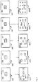
- FIG. 3 depicts various examples of heatsink/arrays of spots of wavelength conversion materials, referred to hereafter as systems 300, 300-1, 300-2, 300-3, 300-4, 300-5, respectively comprising one, four, four, five, six and twelve spots.
- systems 300, 300-1, 300-2, 300-3, 300-4, 300-5 comprise a respective heatsink 305, 305-1, 305-2, 305-3, 305-4, 305-5 similar to heatsink 105, the boundaries of which are represented by an outer large rectangle, and respective spots 307, 307-1, 307-2, 307-3, 307-4, 307-5, each similar to spots 107, represented by smaller rectangles inside respective heatsinks.
- System 300 is depicted above each of systems 300-1, 300-2, 300-3, 300-4, 300-5, with one spot 307 depicted as divided into four, four, five, six and twelve spots using stippled lines, with spot 307 hence having a same wavelength conversion area as, respectively, the total wavelength conversion area of four spots 307-1, four spots 307-2, five spots 307-3, six spots 307-4 and twelve spots 307-5. While each spot 307, 307-1, 307-2, 307-3, 307-4, 307-5 is depicted as rectangular, other shapes of spots 307, 307-1, 307-2, 307-3, 307-4, 307-5 are within the scope of present implementations, including, but not limited to, circular, square, triangular, etc.
- spots 307, 307-1, 307-2, 307-3, 307-4, 307-5 has a same respective shape
- spots 307, 307-1, 307-2, 307-3, 307-4, 307-5 within each set can have different shapes.
- the total wavelength conversion area of each of spots 307, 307-1, 307-2, 307-3, 307-4, 307-5 for each of systems 300-1, 300-2, 300-3, 300-4, 300-5 are all about the same, the total wavelength conversion area not including the spaces in-between spots 307-1, 307-2, 307-3, 307-4, 307-5.
- the area of wavelength conversion material for each of systems 300-1, 300-2, 300-3, 300-4, 300-5 is about the same.
- a respective area of each of spots 307-1 and spots 307-2 is about one quarter an area of spot 307.
- a respective area of each of spots 307-3 is about one fifth an area of spot 307; a respective area of each of spots 307-4 is about one sixth an area of spot 307; and, a respective area of each of spots 307-3 is about one twelfth an area of spot 307.
- spot 307 is assigned a relative wavelength conversion area of unity
- the total wavelength conversion area of each of spots 307-1, 307-2, 307-3, 307-4, 307-5 is unity divided by a number in a range of 4 to 12.
- any of systems 300-1, 300-2, 300-3, 300-4, 300-5 are incorporated into system 100, the array of lenslets 109 is adapted to irradiate respective spots and collect light therefrom as described above.
- any of systems 300-1, 300-2, 300-3, 300-4, 300-5 can be adapted to include any number of spots in a range of 4 spots to 12 spots.
- the temperature limit of the wavelength conversion material remaining unchanged can include a maximum spot temperature being about the same in all configurations (e.g. when the heat removal is increased due to a configuration of spots of wavelength conversion material, the incident power of excitation light can be increased proportionally so that the temperature of a spot is constant between configurations).
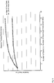
- Fig. 4 depicts relative thermal performance of system 100 adapted for a number of spots 107 ranging from 1 spot to 16 spots, for heatsink 105 having both a "High K” and a "Low K” thermal conductivity.
- a High K thermal conductivity can be about 400 W/mK and a Low K conductivity can be about 150 W/mK.
- the selection of the "High K” and a "Low K” thermal conductivity for Fig. 4 is generally arbitrary and each of the curves in Fig. 4 is meant to demonstrate that relative thermal performance of system 100 remains the same regardless of thermal conductivity of heatsink 105.
- Fig. 4 depicts relative thermal performance of system 100 adapted for a number of spots 107 ranging from 1 spot to 16 spots, for heatsink 105 having both a "High K” and a "Low K” thermal conductivity.
- a High K thermal conductivity can be about 400 W/mK
- a Low K conductivity can be about 150 W/mK.
- Fig. 5 depicts lines heat flux (depicted as stippled lines) in each of heatsink 105, a heatsink 105a, and a heatsink 105b, each of which are similar, other than a number of spots 107, 107a, 107b located thereupon.
- there are four spots 107 on heatsink 105 two spots 107a on heatsink 105a, and one spot 107b on heatsink 105b.
- the respective total areas of spots 107, 107a and 107b are all about the same.
- spots 107 have about the same area as spot 107b, but spots 107 are spread out over a larger area.
- heatsink 105 can dissipate a larger amount of heat than heatsink 105b (e.g. in a same time period).
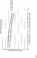
- optical throughput generally decreases as the number of spots 107 increases as depicted in Fig. 6 , which is similar to Fig. 4 , but depicts relative optical throughput of system 100 as a number of spots 107 increases. While optical throughput for heatsink 105 having a relatively High K and a relatively Low K thermal conductivity are depicted as being separated from each other, such separation is only for clarity and in general there is no dependency of optical throughput on the thermal conductivity of heatsink 105. Indeed, each of the curves in Fig. 6 can directly overlap.
- optical throughput generally decreases with a number of spots 107 as spacing between spots begins to limit the angular collection angle of the light 203 by lenslets 109.
- the optical collection efficiency of system 100 decreases with an increasing number of wavelength conversion spots 107 as the spacing between spots 107 begins to limit the angular collection angle of the converted light 203 by lenslets 109.
- the precise decrease is geometrically dependent on a geometry of the array of spots 107 and/or the array of lenslets 109, but the relative decreases depicted in Fig. 6 generally occur.
- the number of spots 107 increase light 203 to be collected by lenslets 109 spreads out so it becomes harder to collect.
- Fig. 7 depicts the curves in Fig. 4 multiplied by the respective curves in Fig. 6 , and hence the combined optical and thermal performance of system 100 as the number of spots 107 increases.
- peak performance occurs in a range of 4 spots to 12 spots, inclusive, as determined empirically, and as indicated by portions of the High K curve that are above line 701, and portions of the Low K curve that are above line 702.
- cost of the array of lenslets 109 can increase after about 12 spots.
- the wavelength conversion area of the array of spots 107 can be selected based on cost and a size of heatsinks available on the market, as well as based on light collection efficiencies. As described above, while present implementations include total wavelength conversion areas of spot arrays disclosed herein can include areas in a range of about 2 mm 2 to about 100mm 2 , cost and optical efficiency can be better in a range of about 4 mm 2 to about 20 mm 2 . In specific non-limiting implementations an area of the array of spots 107 can be about 4.5 mm 2 and/or about 1.5mm x 3mm.
- a distance between spots 107 and a distance between spots 107 and lenslets 109 can also be selected to achieve a balance between heat flow in heatsink 105 and optical collection efficiency of lenslets 109 as described hereafter with reference to Figs. 8 and 9 .
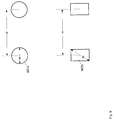
- Fig. 8 depicts a non-limiting implementation of a system 800 that is substantially similar to system 100 with like elements having like numbers, however in an "800" series rather than a "100" series.
- system 800 comprises a heatsink 805, spots 807 of a wavelength conversion material and an array of lenslets 809.
- spots 807 of a wavelength conversion material and an array of lenslets 809.
- system 800 comprises a number of spots 807 in a range of 4 to 12, with a corresponding number of lenslets 809.
- a light source is not depicted, it is appreciated that a light source similar to light source 100 is nonetheless present in system 100, as well as a mirror similar to mirror 150.
- lenslets 809 have a shape different from lenslets 109, system 800 merely demonstrates that various shapes of lenslets are within the scope of present implementations.
- a centre-to-centre distance d between spots 807 which can also be referred to as a spot-spacing distance h.
- lenslets 809, distance h and distance d are selected so that lenslets 809 collect light 833 emitted from spots 807 up to and including about a 75° angle; in other words light up to an emission angle ⁇ of about 75°.
- distance h can be less than abut 5mm, and/or less than about 2mm.
- spots 807 and/or spots 107 etc.
- spacing between spots can be a function of the optical collection angle and distance to lenslet arrays.
- the collection angle can be 75° as described above. As collection angle increases beyond 75°, it becomes harder for the optics of the lenslets to accept and collimate the light. Hence, as a collection angle decreases below 75°, a smaller amount of the emitted light is captured. This accounts for the drop off in optical efficiency in Fig. 6 . Nonetheless, a distance between spots can be selected to balance heat flow with optical efficiency.
- Fig. 9 depicts two sets of example spots 907a and spots 907b, as well as a centre-to-centre distance da between spots 907a and a centre-to-centre distance 2b between spots 907b, distances da, db similar to distance d in Fig. 8 .
- a largest lateral spot dimension ta of spots 907a and a largest lateral spot dimension tb of spots 907b.
- spots 907a as they are circular, the largest lateral spot dimension ta comprises a diameter of each spot 907a, assuming each spot 907a has about the same diameter.
- spots 907b as they are rectangular, the largest lateral spot dimension tb comprises a corner-to-corner diagonal of each spot 907b, assuming each spot 907a has about the same rectangular shape.
- spot shapes are within the scope of present implementations, and hence other largest lateral spot dimension are within the scope of present implementations.
- each spot of wavelength conversion material be the same shape; indeed, in implementations where spots are of different shapes and/or different dimensions, an average largest lateral spot dimension and/or a median largest lateral spot dimension, and the like, could be used in the following determination.
- a balance between optical collection efficiency of lenslets and heat flow in a heatsink can be achieved when a centre-to-centre distance (i.e. distance d, da, db and the like) is between about 5 times and about 25 times, inclusive, the largest lateral spot dimension of spots.
- a balance between optical collection efficiency of lenslets and heat flow in a heatsink can be achieved when a centre-to-centre distance (i.e. distance d, da, db and the like) is between about 10 times and about 20 times, inclusive, the largest lateral spot dimension of spots.
- This can be expressed mathematically as: 5d ⁇ t ⁇ 25d and/or 10d ⁇ t ⁇ 20d, where d is the centre-to-centre distance between spots and t is the largest lateral dimension of spots.
- a system comprising: a light source configured to emit excitation light at an excitation wavelength; a heatsink; a wavelength conversion material located on the heatsink, the wavelength conversion material comprising a relative wavelength conversion area of unity divided into an array of spots, wherein, one or more of 5d ⁇ t ⁇ 25d and 10d ⁇ t ⁇ 20d, where d is a centre-to-centre distance between the spots and t is a largest lateral dimension of the spots, is used to select the centre-to-centre distance between the spots; and, an array of lenslets configured to: receive the excitation light from the light source and irradiate each of the spots of the wavelength conversion material with the excitation light, the lenslets in a one-to-one relationship with the number of spots; and collect the light emitted by the wavelength conversion material.
- a number of spots can be one or more of: greater than or equal to three; in a range of three to twenty, inclusive; and in a range of four to sixteen, inclusive
- a system comprising: a light source configured to emit excitation light at an excitation wavelength; a heatsink; a wavelength conversion material located on the heatsink, the wavelength conversion material comprising a relative wavelength conversion area of unity divided into an array of spots,; and, an array of lenslets configured to: receive the excitation light from the light source and irradiate each of the spots of the wavelength conversion material with the excitation light, the lenslets in a one-to-one relationship with the number of spots; and collect the light emitted by the wavelength conversion material, wherein a distance between a light emitting surface of the spots and a light receiving surface of the lenslets, and a centre-to-centre distance between the spots is selected so that lenslets collect light up to an emission angle ⁇ of about 75° as measured from a normal of the spots.
- a number of spots can be one or more of: greater than or equal to three; in a range of three to twenty, inclusive; and in a range of four to sixteen, inclusive.
- wavelength conversion material on a heatsink is separated into 4 to 12 spots (inclusive) to yield a thermal benefit.
- the exact amount of benefit can be a function of the material properties of the heatsink (particularly the thermal conductivity (K)), heatsink performance, and the spot size and spacing.
- K thermal conductivity
- heatsink performance can be used, which can lead to more light output, as compared to a single spot of wavelength conversion material system.
- other factors can be used to determine a configuration of the spots.
- one or more of 5d ⁇ t ⁇ 25d and 10d ⁇ t ⁇ 20d can be used to select the centre-to-centre distance between the spots; and/or a distance between a light emitting surface of the spots and a light receiving surface of the lenslets, and a centre-to-centre distance between the spots, can be selected so that lenslets collect light up to an emission angle ⁇ of about 75° as measured from a normal of the spots.
- d is a centre-to-centre distance between the spots and t is a largest lateral dimension of the spots
- a distance between a light emitting surface of the spots and a light receiving surface of the lenslets, and a centre-to-centre distance between the spots can be selected so that lenslets collect light up to an emission angle ⁇ of about 75° as measured from a normal of the spots.
- Such factors can be independent of the number of spots, however it is assumed that the number of spots is greater than or equal to three.
Landscapes
- Engineering & Computer Science (AREA)
- General Engineering & Computer Science (AREA)
- Physics & Mathematics (AREA)
- Spectroscopy & Molecular Physics (AREA)
- General Physics & Mathematics (AREA)
- Optics & Photonics (AREA)
- Multimedia (AREA)
- Semiconductor Lasers (AREA)
- Condensed Matter Physics & Semiconductors (AREA)
- Electromagnetism (AREA)
Applications Claiming Priority (1)
| Application Number | Priority Date | Filing Date | Title |
|---|---|---|---|
| US14/639,269 US9726348B2 (en) | 2015-03-05 | 2015-03-05 | Wavelength conversion material array |
Publications (2)
| Publication Number | Publication Date |
|---|---|
| EP3065187A1 true EP3065187A1 (de) | 2016-09-07 |
| EP3065187B1 EP3065187B1 (de) | 2019-03-27 |
Family
ID=55398198
Family Applications (1)
| Application Number | Title | Priority Date | Filing Date |
|---|---|---|---|
| EP16155480.3A Active EP3065187B1 (de) | 2015-03-05 | 2016-02-12 | Wellenlängenumwandlungsmaterialanordnung |
Country Status (3)
| Country | Link |
|---|---|
| US (1) | US9726348B2 (de) |
| EP (1) | EP3065187B1 (de) |
| CN (1) | CN105938293B (de) |
Cited By (1)
| Publication number | Priority date | Publication date | Assignee | Title |
|---|---|---|---|---|
| CN113495419A (zh) * | 2020-04-07 | 2021-10-12 | 深圳光峰科技股份有限公司 | 光源系统以及投影显示装置 |
Families Citing this family (2)
| Publication number | Priority date | Publication date | Assignee | Title |
|---|---|---|---|---|
| EP3475988B1 (de) * | 2016-06-22 | 2022-08-10 | Lumileds LLC | Beleuchtungssystem |
| CN108319096B (zh) * | 2017-01-17 | 2020-12-15 | 深圳光峰科技股份有限公司 | 一种荧光芯片及其显示系统 |
Citations (3)
| Publication number | Priority date | Publication date | Assignee | Title |
|---|---|---|---|---|
| EP1605199A2 (de) * | 2004-06-04 | 2005-12-14 | LumiLeds Lighting U.S., LLC | Ferngesteuerte Wellenlänge Konversion in Beleuchtungsvorrichtung |
| WO2009115976A1 (en) * | 2008-03-20 | 2009-09-24 | Koninklijke Philips Electronics N.V. | Illumination system comprising a luminescent element with a heat sink |
| US20140084325A1 (en) * | 2011-07-12 | 2014-03-27 | Panasonic Corporation | Optical element and semiconductor light emitting device using the optical element |
Family Cites Families (16)
| Publication number | Priority date | Publication date | Assignee | Title |
|---|---|---|---|---|
| US3639138A (en) | 1968-05-27 | 1972-02-01 | Texas Instruments Inc | Phosphor screen fabrication |
| US4023064A (en) * | 1972-08-08 | 1977-05-10 | U.S. Philips Corporation | Channel plate with color selection electrodes and color phosphors |
| US5835515A (en) * | 1996-10-25 | 1998-11-10 | Lucent Technologies Inc. | High power semiconductor laser array |
| US6400513B1 (en) * | 2000-03-15 | 2002-06-04 | Quantum Devices, Inc. | Optical beam coupling of multiple wavelengths into an output channel using spatial wavefront segmentation |
| JP2001288467A (ja) * | 2000-04-06 | 2001-10-16 | Toshiba Corp | 酸化物複合体粒子とその製造方法、蛍光体とその製造方法、カラーフィルターとその製造方法、ならびにカラー表示装置 |
| JP2005158273A (ja) * | 2003-11-20 | 2005-06-16 | Toshiba Corp | 画像表示装置 |
| US20090122272A1 (en) * | 2007-11-09 | 2009-05-14 | Silverstein Barry D | Projection apparatus using solid-state light source array |
| US20100149222A1 (en) * | 2008-07-10 | 2010-06-17 | Corporation For Laser Optics Research | Blue laser pumped green light source for displays |
| US8132919B2 (en) * | 2009-04-30 | 2012-03-13 | Eastman Kodak Company | Digital projector using arrayed light sources |
| US8142021B2 (en) * | 2009-06-25 | 2012-03-27 | Eastman Kodak Company | Dump path light intensity sensing in light projector |
| CN103365051B (zh) * | 2012-04-01 | 2016-08-03 | 欧司朗股份有限公司 | 照明装置及投影仪 |
| US8934173B2 (en) * | 2012-08-21 | 2015-01-13 | Svv Technology Innovations, Inc. | Optical article for illuminating building interiors with sunlight |
| CN104769497B (zh) * | 2012-11-07 | 2016-09-28 | 松下知识产权经营株式会社 | 光源以及图像投影装置 |
| EP2989375B1 (de) * | 2013-03-12 | 2019-12-11 | Seoul Semiconductor Co., Ltd. | Schmale leuchte |
| WO2014202456A1 (en) * | 2013-06-20 | 2014-12-24 | Koninklijke Philips N.V. | Lighting device comprising at least two sets of leds |
| WO2015000716A1 (en) * | 2013-07-04 | 2015-01-08 | Koninklijke Philips N.V. | Lighting device with an optical element having a fluid passage |
-
2015
- 2015-03-05 US US14/639,269 patent/US9726348B2/en active Active
-
2016
- 2016-02-12 EP EP16155480.3A patent/EP3065187B1/de active Active
- 2016-03-03 CN CN201610120686.7A patent/CN105938293B/zh not_active Expired - Fee Related
Patent Citations (3)
| Publication number | Priority date | Publication date | Assignee | Title |
|---|---|---|---|---|
| EP1605199A2 (de) * | 2004-06-04 | 2005-12-14 | LumiLeds Lighting U.S., LLC | Ferngesteuerte Wellenlänge Konversion in Beleuchtungsvorrichtung |
| WO2009115976A1 (en) * | 2008-03-20 | 2009-09-24 | Koninklijke Philips Electronics N.V. | Illumination system comprising a luminescent element with a heat sink |
| US20140084325A1 (en) * | 2011-07-12 | 2014-03-27 | Panasonic Corporation | Optical element and semiconductor light emitting device using the optical element |
Cited By (1)
| Publication number | Priority date | Publication date | Assignee | Title |
|---|---|---|---|---|
| CN113495419A (zh) * | 2020-04-07 | 2021-10-12 | 深圳光峰科技股份有限公司 | 光源系统以及投影显示装置 |
Also Published As
| Publication number | Publication date |
|---|---|
| US9726348B2 (en) | 2017-08-08 |
| HK1224384A1 (zh) | 2017-08-18 |
| EP3065187B1 (de) | 2019-03-27 |
| US20160258597A1 (en) | 2016-09-08 |
| CN105938293A (zh) | 2016-09-14 |
| CN105938293B (zh) | 2018-04-10 |
Similar Documents
| Publication | Publication Date | Title |
|---|---|---|
| US9223196B2 (en) | Lighting device comprising pump light source and at least two phosphor wheels | |
| US9869453B2 (en) | Light source, light source unit, and light source module using same | |
| JP6924923B2 (ja) | 蛍光体ホイール装置、照明装置、及び投写型映像表示装置 | |
| EP2988170B1 (de) | Lichtemittierende vorrichtung und zugehöriges projektionssystem | |
| CN105299603B (zh) | 光发生系统 | |
| US20150042963A1 (en) | Light source device and image projecting apparatus having the same | |
| US9476573B2 (en) | Lighting apparatus comprising phosphor wheel | |
| US20130107226A1 (en) | Projection system comprising a solid state light source and a luminsecent material | |
| US20120217519A1 (en) | Method and structure for encapsulating solid-state light emitting chip and light sources using the encapsulation structure | |
| EP3065187B1 (de) | Wellenlängenumwandlungsmaterialanordnung | |
| WO2017061227A1 (ja) | 蛍光光源装置 | |
| CN106796346B (zh) | 借助于光学装置处理光 | |
| WO2012004713A1 (en) | Projection system comprising a solid state light source and a luminescent material | |
| EP3669115B1 (de) | Breitbandige lichtquelle auf der basis von kristallinem leuchtstoff | |
| Daniels et al. | Laser-activated remote phosphor light engine for projection applications | |
| JP5802354B2 (ja) | 高い輝度のソリッドステート光源 | |
| US20190339600A1 (en) | Wavelength conversion device, light source device, and projector | |
| HK1224384B (en) | Wavelength conversion material array | |
| WO2019124120A1 (ja) | 光学ユニットおよび投射型表示装置 | |
| JP6663579B2 (ja) | 光源装置 | |
| CN116615621A (zh) | 荧光体轮以及投射型图像显示装置 | |
| JP6866627B2 (ja) | 照明装置及びプロジェクター | |
| WO2025204599A1 (ja) | 光源装置 |
Legal Events
| Date | Code | Title | Description |
|---|---|---|---|
| PUAI | Public reference made under article 153(3) epc to a published international application that has entered the european phase |
Free format text: ORIGINAL CODE: 0009012 |
|
| AK | Designated contracting states |
Kind code of ref document: A1 Designated state(s): AL AT BE BG CH CY CZ DE DK EE ES FI FR GB GR HR HU IE IS IT LI LT LU LV MC MK MT NL NO PL PT RO RS SE SI SK SM TR |
|
| AX | Request for extension of the european patent |
Extension state: BA ME |
|
| STAA | Information on the status of an ep patent application or granted ep patent |
Free format text: STATUS: REQUEST FOR EXAMINATION WAS MADE |
|
| 17P | Request for examination filed |
Effective date: 20170214 |
|
| RBV | Designated contracting states (corrected) |
Designated state(s): AL AT BE BG CH CY CZ DE DK EE ES FI FR GB GR HR HU IE IS IT LI LT LU LV MC MK MT NL NO PL PT RO RS SE SI SK SM TR |
|
| GRAP | Despatch of communication of intention to grant a patent |
Free format text: ORIGINAL CODE: EPIDOSNIGR1 |
|
| STAA | Information on the status of an ep patent application or granted ep patent |
Free format text: STATUS: GRANT OF PATENT IS INTENDED |
|
| INTG | Intention to grant announced |
Effective date: 20180904 |
|
| GRAS | Grant fee paid |
Free format text: ORIGINAL CODE: EPIDOSNIGR3 |
|
| GRAA | (expected) grant |
Free format text: ORIGINAL CODE: 0009210 |
|
| STAA | Information on the status of an ep patent application or granted ep patent |
Free format text: STATUS: THE PATENT HAS BEEN GRANTED |
|
| AK | Designated contracting states |
Kind code of ref document: B1 Designated state(s): AL AT BE BG CH CY CZ DE DK EE ES FI FR GB GR HR HU IE IS IT LI LT LU LV MC MK MT NL NO PL PT RO RS SE SI SK SM TR |
|
| REG | Reference to a national code |
Ref country code: GB Ref legal event code: FG4D |
|
| REG | Reference to a national code |
Ref country code: CH Ref legal event code: EP |
|
| REG | Reference to a national code |
Ref country code: AT Ref legal event code: REF Ref document number: 1114081 Country of ref document: AT Kind code of ref document: T Effective date: 20190415 |
|
| REG | Reference to a national code |
Ref country code: IE Ref legal event code: FG4D |
|
| REG | Reference to a national code |
Ref country code: DE Ref legal event code: R096 Ref document number: 602016011432 Country of ref document: DE |
|
| PG25 | Lapsed in a contracting state [announced via postgrant information from national office to epo] |
Ref country code: FI Free format text: LAPSE BECAUSE OF FAILURE TO SUBMIT A TRANSLATION OF THE DESCRIPTION OR TO PAY THE FEE WITHIN THE PRESCRIBED TIME-LIMIT Effective date: 20190327 Ref country code: NO Free format text: LAPSE BECAUSE OF FAILURE TO SUBMIT A TRANSLATION OF THE DESCRIPTION OR TO PAY THE FEE WITHIN THE PRESCRIBED TIME-LIMIT Effective date: 20190627 Ref country code: LT Free format text: LAPSE BECAUSE OF FAILURE TO SUBMIT A TRANSLATION OF THE DESCRIPTION OR TO PAY THE FEE WITHIN THE PRESCRIBED TIME-LIMIT Effective date: 20190327 Ref country code: SE Free format text: LAPSE BECAUSE OF FAILURE TO SUBMIT A TRANSLATION OF THE DESCRIPTION OR TO PAY THE FEE WITHIN THE PRESCRIBED TIME-LIMIT Effective date: 20190327 |
|
| REG | Reference to a national code |
Ref country code: NL Ref legal event code: MP Effective date: 20190327 |
|
| PG25 | Lapsed in a contracting state [announced via postgrant information from national office to epo] |
Ref country code: NL Free format text: LAPSE BECAUSE OF FAILURE TO SUBMIT A TRANSLATION OF THE DESCRIPTION OR TO PAY THE FEE WITHIN THE PRESCRIBED TIME-LIMIT Effective date: 20190327 Ref country code: LV Free format text: LAPSE BECAUSE OF FAILURE TO SUBMIT A TRANSLATION OF THE DESCRIPTION OR TO PAY THE FEE WITHIN THE PRESCRIBED TIME-LIMIT Effective date: 20190327 Ref country code: RS Free format text: LAPSE BECAUSE OF FAILURE TO SUBMIT A TRANSLATION OF THE DESCRIPTION OR TO PAY THE FEE WITHIN THE PRESCRIBED TIME-LIMIT Effective date: 20190327 Ref country code: BG Free format text: LAPSE BECAUSE OF FAILURE TO SUBMIT A TRANSLATION OF THE DESCRIPTION OR TO PAY THE FEE WITHIN THE PRESCRIBED TIME-LIMIT Effective date: 20190627 Ref country code: GR Free format text: LAPSE BECAUSE OF FAILURE TO SUBMIT A TRANSLATION OF THE DESCRIPTION OR TO PAY THE FEE WITHIN THE PRESCRIBED TIME-LIMIT Effective date: 20190628 Ref country code: HR Free format text: LAPSE BECAUSE OF FAILURE TO SUBMIT A TRANSLATION OF THE DESCRIPTION OR TO PAY THE FEE WITHIN THE PRESCRIBED TIME-LIMIT Effective date: 20190327 |
|
| REG | Reference to a national code |
Ref country code: AT Ref legal event code: MK05 Ref document number: 1114081 Country of ref document: AT Kind code of ref document: T Effective date: 20190327 |
|
| PG25 | Lapsed in a contracting state [announced via postgrant information from national office to epo] |
Ref country code: ES Free format text: LAPSE BECAUSE OF FAILURE TO SUBMIT A TRANSLATION OF THE DESCRIPTION OR TO PAY THE FEE WITHIN THE PRESCRIBED TIME-LIMIT Effective date: 20190327 Ref country code: AL Free format text: LAPSE BECAUSE OF FAILURE TO SUBMIT A TRANSLATION OF THE DESCRIPTION OR TO PAY THE FEE WITHIN THE PRESCRIBED TIME-LIMIT Effective date: 20190327 Ref country code: PT Free format text: LAPSE BECAUSE OF FAILURE TO SUBMIT A TRANSLATION OF THE DESCRIPTION OR TO PAY THE FEE WITHIN THE PRESCRIBED TIME-LIMIT Effective date: 20190727 Ref country code: SK Free format text: LAPSE BECAUSE OF FAILURE TO SUBMIT A TRANSLATION OF THE DESCRIPTION OR TO PAY THE FEE WITHIN THE PRESCRIBED TIME-LIMIT Effective date: 20190327 Ref country code: RO Free format text: LAPSE BECAUSE OF FAILURE TO SUBMIT A TRANSLATION OF THE DESCRIPTION OR TO PAY THE FEE WITHIN THE PRESCRIBED TIME-LIMIT Effective date: 20190327 Ref country code: CZ Free format text: LAPSE BECAUSE OF FAILURE TO SUBMIT A TRANSLATION OF THE DESCRIPTION OR TO PAY THE FEE WITHIN THE PRESCRIBED TIME-LIMIT Effective date: 20190327 Ref country code: EE Free format text: LAPSE BECAUSE OF FAILURE TO SUBMIT A TRANSLATION OF THE DESCRIPTION OR TO PAY THE FEE WITHIN THE PRESCRIBED TIME-LIMIT Effective date: 20190327 |
|
| PG25 | Lapsed in a contracting state [announced via postgrant information from national office to epo] |
Ref country code: SM Free format text: LAPSE BECAUSE OF FAILURE TO SUBMIT A TRANSLATION OF THE DESCRIPTION OR TO PAY THE FEE WITHIN THE PRESCRIBED TIME-LIMIT Effective date: 20190327 Ref country code: PL Free format text: LAPSE BECAUSE OF FAILURE TO SUBMIT A TRANSLATION OF THE DESCRIPTION OR TO PAY THE FEE WITHIN THE PRESCRIBED TIME-LIMIT Effective date: 20190327 |
|
| PG25 | Lapsed in a contracting state [announced via postgrant information from national office to epo] |
Ref country code: IS Free format text: LAPSE BECAUSE OF FAILURE TO SUBMIT A TRANSLATION OF THE DESCRIPTION OR TO PAY THE FEE WITHIN THE PRESCRIBED TIME-LIMIT Effective date: 20190727 Ref country code: AT Free format text: LAPSE BECAUSE OF FAILURE TO SUBMIT A TRANSLATION OF THE DESCRIPTION OR TO PAY THE FEE WITHIN THE PRESCRIBED TIME-LIMIT Effective date: 20190327 |
|
| REG | Reference to a national code |
Ref country code: DE Ref legal event code: R097 Ref document number: 602016011432 Country of ref document: DE |
|
| PG25 | Lapsed in a contracting state [announced via postgrant information from national office to epo] |
Ref country code: DK Free format text: LAPSE BECAUSE OF FAILURE TO SUBMIT A TRANSLATION OF THE DESCRIPTION OR TO PAY THE FEE WITHIN THE PRESCRIBED TIME-LIMIT Effective date: 20190327 |
|
| PLBE | No opposition filed within time limit |
Free format text: ORIGINAL CODE: 0009261 |
|
| STAA | Information on the status of an ep patent application or granted ep patent |
Free format text: STATUS: NO OPPOSITION FILED WITHIN TIME LIMIT |
|
| PG25 | Lapsed in a contracting state [announced via postgrant information from national office to epo] |
Ref country code: SI Free format text: LAPSE BECAUSE OF FAILURE TO SUBMIT A TRANSLATION OF THE DESCRIPTION OR TO PAY THE FEE WITHIN THE PRESCRIBED TIME-LIMIT Effective date: 20190327 |
|
| 26N | No opposition filed |
Effective date: 20200103 |
|
| PG25 | Lapsed in a contracting state [announced via postgrant information from national office to epo] |
Ref country code: TR Free format text: LAPSE BECAUSE OF FAILURE TO SUBMIT A TRANSLATION OF THE DESCRIPTION OR TO PAY THE FEE WITHIN THE PRESCRIBED TIME-LIMIT Effective date: 20190327 |
|
| REG | Reference to a national code |
Ref country code: DE Ref legal event code: R119 Ref document number: 602016011432 Country of ref document: DE |
|
| REG | Reference to a national code |
Ref country code: CH Ref legal event code: PL |
|
| GBPC | Gb: european patent ceased through non-payment of renewal fee |
Effective date: 20200212 |
|
| REG | Reference to a national code |
Ref country code: BE Ref legal event code: MM Effective date: 20200229 |
|
| PG25 | Lapsed in a contracting state [announced via postgrant information from national office to epo] |
Ref country code: MC Free format text: LAPSE BECAUSE OF FAILURE TO SUBMIT A TRANSLATION OF THE DESCRIPTION OR TO PAY THE FEE WITHIN THE PRESCRIBED TIME-LIMIT Effective date: 20190327 Ref country code: LU Free format text: LAPSE BECAUSE OF NON-PAYMENT OF DUE FEES Effective date: 20200212 |
|
| PG25 | Lapsed in a contracting state [announced via postgrant information from national office to epo] |
Ref country code: CH Free format text: LAPSE BECAUSE OF NON-PAYMENT OF DUE FEES Effective date: 20200229 Ref country code: LI Free format text: LAPSE BECAUSE OF NON-PAYMENT OF DUE FEES Effective date: 20200229 |
|
| PG25 | Lapsed in a contracting state [announced via postgrant information from national office to epo] |
Ref country code: FR Free format text: LAPSE BECAUSE OF NON-PAYMENT OF DUE FEES Effective date: 20200229 Ref country code: GB Free format text: LAPSE BECAUSE OF NON-PAYMENT OF DUE FEES Effective date: 20200212 Ref country code: IE Free format text: LAPSE BECAUSE OF NON-PAYMENT OF DUE FEES Effective date: 20200212 Ref country code: DE Free format text: LAPSE BECAUSE OF NON-PAYMENT OF DUE FEES Effective date: 20200901 |
|
| PG25 | Lapsed in a contracting state [announced via postgrant information from national office to epo] |
Ref country code: BE Free format text: LAPSE BECAUSE OF NON-PAYMENT OF DUE FEES Effective date: 20200229 |
|
| PG25 | Lapsed in a contracting state [announced via postgrant information from national office to epo] |
Ref country code: IT Free format text: LAPSE BECAUSE OF NON-PAYMENT OF DUE FEES Effective date: 20200212 |
|
| PG25 | Lapsed in a contracting state [announced via postgrant information from national office to epo] |
Ref country code: MT Free format text: LAPSE BECAUSE OF FAILURE TO SUBMIT A TRANSLATION OF THE DESCRIPTION OR TO PAY THE FEE WITHIN THE PRESCRIBED TIME-LIMIT Effective date: 20190327 Ref country code: CY Free format text: LAPSE BECAUSE OF FAILURE TO SUBMIT A TRANSLATION OF THE DESCRIPTION OR TO PAY THE FEE WITHIN THE PRESCRIBED TIME-LIMIT Effective date: 20190327 |
|
| PG25 | Lapsed in a contracting state [announced via postgrant information from national office to epo] |
Ref country code: MK Free format text: LAPSE BECAUSE OF FAILURE TO SUBMIT A TRANSLATION OF THE DESCRIPTION OR TO PAY THE FEE WITHIN THE PRESCRIBED TIME-LIMIT Effective date: 20190327 |
|
| P01 | Opt-out of the competence of the unified patent court (upc) registered |
Effective date: 20230523 |