EP3065218A1 - Dispositif électronique comprenant un ensemble d'antenne à plaque ayant des points d'alimentation capacitive et des trous d'interconnexion de blindage de conducteurs espacés et procédés associés - Google Patents
Dispositif électronique comprenant un ensemble d'antenne à plaque ayant des points d'alimentation capacitive et des trous d'interconnexion de blindage de conducteurs espacés et procédés associés Download PDFInfo
- Publication number
- EP3065218A1 EP3065218A1 EP16000446.1A EP16000446A EP3065218A1 EP 3065218 A1 EP3065218 A1 EP 3065218A1 EP 16000446 A EP16000446 A EP 16000446A EP 3065218 A1 EP3065218 A1 EP 3065218A1
- Authority
- EP
- European Patent Office
- Prior art keywords
- electrically conductive
- feed
- patch antenna
- substrate
- antenna element
- Prior art date
- Legal status (The legal status is an assumption and is not a legal conclusion. Google has not performed a legal analysis and makes no representation as to the accuracy of the status listed.)
- Granted
Links
Images





Classifications
-
- H—ELECTRICITY
- H01—ELECTRIC ELEMENTS
- H01Q—ANTENNAS, i.e. RADIO AERIALS
- H01Q1/00—Details of, or arrangements associated with, antennas
- H01Q1/52—Means for reducing coupling between antennas; Means for reducing coupling between an antenna and another structure
- H01Q1/526—Electromagnetic shields
-
- H—ELECTRICITY
- H01—ELECTRIC ELEMENTS
- H01Q—ANTENNAS, i.e. RADIO AERIALS
- H01Q1/00—Details of, or arrangements associated with, antennas
- H01Q1/36—Structural form of radiating elements, e.g. cone, spiral, umbrella; Particular materials used therewith
- H01Q1/38—Structural form of radiating elements, e.g. cone, spiral, umbrella; Particular materials used therewith formed by a conductive layer on an insulating support
-
- H—ELECTRICITY
- H01—ELECTRIC ELEMENTS
- H01Q—ANTENNAS, i.e. RADIO AERIALS
- H01Q1/00—Details of, or arrangements associated with, antennas
- H01Q1/48—Earthing means; Earth screens; Counterpoises
-
- H—ELECTRICITY
- H01—ELECTRIC ELEMENTS
- H01Q—ANTENNAS, i.e. RADIO AERIALS
- H01Q1/00—Details of, or arrangements associated with, antennas
- H01Q1/52—Means for reducing coupling between antennas; Means for reducing coupling between an antenna and another structure
-
- H—ELECTRICITY
- H01—ELECTRIC ELEMENTS
- H01Q—ANTENNAS, i.e. RADIO AERIALS
- H01Q9/00—Electrically-short antennas having dimensions not more than twice the operating wavelength and consisting of conductive active radiating elements
- H01Q9/04—Resonant antennas
- H01Q9/0407—Substantially flat resonant element parallel to ground plane, e.g. patch antenna
-
- H—ELECTRICITY
- H01—ELECTRIC ELEMENTS
- H01Q—ANTENNAS, i.e. RADIO AERIALS
- H01Q9/00—Electrically-short antennas having dimensions not more than twice the operating wavelength and consisting of conductive active radiating elements
- H01Q9/04—Resonant antennas
- H01Q9/0407—Substantially flat resonant element parallel to ground plane, e.g. patch antenna
- H01Q9/0442—Substantially flat resonant element parallel to ground plane, e.g. patch antenna with particular tuning means
-
- H—ELECTRICITY
- H01—ELECTRIC ELEMENTS
- H01Q—ANTENNAS, i.e. RADIO AERIALS
- H01Q9/00—Electrically-short antennas having dimensions not more than twice the operating wavelength and consisting of conductive active radiating elements
- H01Q9/04—Resonant antennas
- H01Q9/0407—Substantially flat resonant element parallel to ground plane, e.g. patch antenna
- H01Q9/045—Substantially flat resonant element parallel to ground plane, e.g. patch antenna with particular feeding means
-
- H—ELECTRICITY
- H01—ELECTRIC ELEMENTS
- H01Q—ANTENNAS, i.e. RADIO AERIALS
- H01Q9/00—Electrically-short antennas having dimensions not more than twice the operating wavelength and consisting of conductive active radiating elements
- H01Q9/04—Resonant antennas
- H01Q9/0407—Substantially flat resonant element parallel to ground plane, e.g. patch antenna
- H01Q9/045—Substantially flat resonant element parallel to ground plane, e.g. patch antenna with particular feeding means
- H01Q9/0457—Substantially flat resonant element parallel to ground plane, e.g. patch antenna with particular feeding means electromagnetically coupled to the feed line
-
- H—ELECTRICITY
- H01—ELECTRIC ELEMENTS
- H01Q—ANTENNAS, i.e. RADIO AERIALS
- H01Q9/00—Electrically-short antennas having dimensions not more than twice the operating wavelength and consisting of conductive active radiating elements
- H01Q9/04—Resonant antennas
- H01Q9/0407—Substantially flat resonant element parallel to ground plane, e.g. patch antenna
- H01Q9/0478—Substantially flat resonant element parallel to ground plane, e.g. patch antenna with means for suppressing spurious modes, e.g. cross polarisation
Definitions
- the present invention relates to the field of electronic devices, and, more particularly, to patch antennas and related methods.
- a patch antenna for example, a microstrip patch antenna may provide a relatively a high gain for a given area using a relatively simple printed circuit construction, thus making its use widespread.
- One type of microstrip patch antenna has a radiation pattern that extends broadside to the patch plane.
- Such a microstrip antenna is commonly fed using a probe, for example, in the form of a connector pin or a circuit board via to form the probe that carries current to the patch surfaces.
- the radiation bandwidth of a microstrip patch antenna may be limited.
- the half power (3 dB) instantaneous gain bandwidth of microstrip patch antennas may be less than 20 percent in practice. This may be particularly disadvantageous compared to other types of antennas, such as parabolic reflector antennas, which can operate over many octaves of bandwidth.
- the bandwidth of a microstrip patch antenna increases linearly based upon the thickness of the substrate on which it is carried, so doubling the substrate thickness may double the bandwidth and halving the substrate thickness may halve the bandwidth.
- problems may arise in a broadband application using a relatively thick substrate microstrip antenna, as the feed probe can radiate in a manner akin to a monopole antenna. Given that the radiation pattern of a feed probe is different than that of the patch itself, the combined thick substrate patch radiation produces an asymmetric pattern and reduced realized gain.
- U.S. Patent No. 6,181,279 to Van Hoozen discloses a patch antenna with an electrically small ground plate using peripheral parasitic stubs. More particularly, Van Hoozen discloses the parasitic stubs or shielding element is for segregating electromagnetic fields between the patch antenna and the ground plate.
- U.S. Patent No. 5,515,057 to Lennen et al. is directed to a GPS receiver with an n-point symmetrical feed double-frequency patch antenna. More particularly, Lennen et al. discloses n symmetrical feed points that are placed geometrically on the patch antenna to achieve circular polarization of the GPS receiver with an n-point antenna.
- patch antennas may be desired. For example, it may be particularly desirable to increase bandwidth, gain, directivity, and radiation pattern symmetry.
- An electronic device may include wireless communications circuitry, and an antenna assembly coupled to the wireless communications circuitry.
- the antenna assembly may include a substrate, an electrically conductive layer defining a ground plane carried by the substrate, and an electrically conductive patch antenna element carried by the substrate and spaced from the ground plane.
- the electrically conductive patch antenna element may have a symmetric axis dividing the electrically conductive patch antenna element into first and second symmetric areas.
- the electrically conductive patch antenna element may have first and second feed openings in the first and second symmetric areas, respectively, and first and second feed pads in the first and second feed openings, respectively, defining first and second capacitive feed points.
- the antenna assembly may also include first and second feed lines extending through the substrate and respectively coupling the first and second feed pads to the wireless communications circuitry, and a plurality of spaced apart conductive shielding vias coupled to the ground plane and extending through the substrate surrounding the electrically conductive patch antenna element. Accordingly, the electronic device may provide increased efficiency, for example, by providing increased bandwidth, gain, and directivity.
- the electrically conductive patch antenna element may have at least one bucking opening therein.
- the substrate may include at least one bucking recess aligned with the at least one bucking opening, for example.
- the antenna assembly may further include at least one conductive bucking via coupled to the ground plane and extending to the at least one bucking recess, for example.
- the electronic device may further include phase delay circuitry carried by the substrate and coupled to at least one of the first and second feed lines.
- the phase delay circuitry may include at least one meander line, for example.
- the antenna assembly may further include at least one resonator coupled to each of the first and second capacitive feed points.
- the at least one resonator may include at least one conductive X-shaped resonator, for example.
- the electronic device may further include a dielectric cover layer carried by the electrically conductive patch antenna element.
- the dielectric cover layer may have a relative permittivity and a relative permittivity within 20% of each other.
- the substrate may have a relative permittivity and a relative permittivity within 20% of each other, for example.
- a method aspect is directed to a method of making an antenna assembly.
- the method may include forming an electrically conductive patch antenna element on a substrate and spaced from an electrically conductive layer defining a ground plane.
- the electrically conductive patch antenna element may be formed to have a symmetric axis dividing the electrically conductive patch antenna element into first and second symmetric areas.
- the electrically conductive patch antenna element may be formed to have first and second feed openings in the first and second symmetric areas, respectively.
- the method may further include forming first and second feed pads in the first and second feed openings, respectively, defining first and second capacitive feed points.
- the method may also include forming first and second feed lines extending through the substrate and respectively coupling the first and second feed pads to wireless communications circuitry, and forming a plurality of spaced apart conductive shielding vias coupled to the ground plane and extending through the substrate surrounding the electrically conductive patch antenna element.
- the antenna assembly may include a substrate, an electrically conductive layer defining a ground plane carried by the substrate, and an electrically conductive patch antenna element carried by the substrate and spaced from the ground plane.
- the electrically conductive patch antenna may have a symmetric axis dividing the electrically conductive patch antenna element into first and second symmetric areas.
- the electrically conductive patch may have first and second feed openings in the first and second symmetric areas, respectively, and first and second feed pads in the first and second feed openings, respectively, defining first and second capacitive feed points.
- the antenna assembly may also include first and second feed lines extending through the substrate, one of the first and second feed lines coupling a respective one of the first and second feed pads to the wireless communications circuitry and another of the first and second feed lines being electrically floating, and a plurality of spaced apart conductive shielding vias coupled to the ground plane and extending through the substrate surrounding the electrically conductive patch antenna element.
- the ground plane may have at least one opening therein.
- the substrate may include at least one recess aligned with the at least one opening, for example.
- the another one of the first and second feed lines may extend to the at least one recess.
- the antenna assembly may further include at least one resonator coupled to each of the first and second capacitive feed points.
- the at least one resonator may be an X-shaped resonator.
- the electronic device may further include a dielectric cover layer carried by the electrically conductive patch antenna element.
- the dielectric cover layer may have a relative permittivity and a relative permittivity within 20% of each other.
- the substrate may have a relative permittivity and a relative permittivity within 20% of each other, for example.
- a corresponding method of making an antenna assembly may include forming an electrically conductive patch antenna element on a substrate and spaced from an electrically conductive layer defining a ground plane ground plane.
- the electrically conductive patch antenna may be formed to have a symmetric axis dividing the electrically conductive patch antenna element into first and second symmetric areas.
- the electrically conductive patch antenna element may also be formed to have first and second feed openings in the first and second symmetric areas, respectively.
- the method may also include forming first and second feed pads in the first and second feed openings, respectively, defining first and second capacitive feed points and forming first and second feed lines extending through the substrate, one of the first and second feed lines coupling a respective one of the first and second feed pads to wireless communications circuitry and another of the first and second feed lines being electrically floating.
- the method may further include forming a plurality of spaced apart conductive shielding vias coupled to the ground plane and extending through the substrate surrounding the electrically conductive patch antenna element.
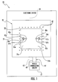
- an electronic device 20 includes wireless communications circuitry 21 and an antenna assembly 30 coupled to the wireless communications circuitry.
- the wireless communications circuitry 21 may include a wireless transceiver, just a transmitter, just a receiver, and/or an RF power source, for example.
- the wireless communications circuitry 21 may include other and/or additional circuitry for wireless communication.
- the antenna assembly 30 may be considered a reciprocal device useful for both transmitting and receiving.
- the antenna assembly 30 may be in the form of a microstrip patch antenna for linear polarization, and illustratively includes a substrate 31 and an electrically conductive layer defining a ground plane 32 carried by the substrate.
- the ground plane 32 is illustratively carried within the substrate 31 , for example, sandwiched between two dielectric layers of the substrate. In some embodiments, the ground plane 32 may be carried by a lower surface of the substrate 31 or by another portion of the substrate.
- the antenna assembly 30 may be realized as a multilayer circuit board. Additional ground plane layers may be included.
- the antenna assembly 30 also includes an electrically conductive patch antenna element 33 carried by an upper surface of the substrate 31 .
- the electrically conductive patch antenna element 33 is illustratively spaced from the ground plane 32 .
- the electrically conductive patch antenna element 33 illustratively is in the shape of a rectangle, and more particularly, a square. Of course the electrically conductive patch antenna element 33 may have another shape, for example, a circular shape.
- the electrically conductive patch antenna element 33 has a symmetric axis 34 that divides the electrically conductive patch antenna element into first and second symmetric areas 35a, 35b.
- the electrically conductive patch antenna element 33 has first and second feed openings 36a, 36b in the first and second symmetric areas 35a, 35b , respectively. While a particular symmetric axis 34 is illustrated, it should be understood that the symmetric axis may be aligned differently than as illustrated, for example, it may be diagonally oriented.
- the electrically conductive patch antenna element 33 also includes first and second feed pads in the first and second feed openings 36a , 36b , respectively, defining first and second capacitive feed points 37a , 37b .
- the electrically conductive patch antenna element 33 also includes first and second feed lines 41a , 41b extending through the substrate 31 and respectively coupling the first and second feed pads or first and second capacitive feed points 37a , 37b to the wireless communications circuitry 21 .
- the first and second feed lines 41 a, 41b may be in the form of a plated through-hole via, a metal connector pin, rivet, hookup wire, or other feed structure as will be appreciated by those skilled in the art.
- the first and second capacitive feed points 37a, 37b capacitively couple currents to the electrically conductive patch antenna element 33 across the air gap therebetween.
- the first and second capacitive feed points 37a , 37b may cancel distributed inductance of the first and second feed lines 41a , 41b .
- Distributed inductance of the first and second feed lines 41a , 41b and the distributed capacitance of the first and second capacitive feed points 37a, 37b together form a series resonant circuit which may provide a double tuned antenna system for increased bandwidth.
- the double tuning may form a 4 th order Chebyschev response with, selected for passband ripple, a maximally flat Butterworth response, or other response shapes as will be appreciated by those skilled in the art.
- the first and second capacitive feed points 37a , 37b are illustratively oriented as a diamond shape relative to the electrically conductive patch antenna element 33 . This may reduce reflections to the passage of currents on the surface of the electrically conductive patch antenna element 33 .
- the first and second capacitive feed points 37a, 37b may be oriented as a square, i.e., aligned with, the electrically conductive patch antenna element 33 , or have other shapes as well.
- Radiation from the second feed line 41b is toward the opposite side of the electrically conductive patch antenna element 33 than radiation from the first feed line 41a. Radiation from the first and second feed lines 41a , 41b may therefore counteract each other to produce a more symmetric radiation pattern with a beam maximum more normal to the electrically conductive patch antenna element 33 . It may be desirable to drive the first and second feed lines 41a , 41b at equal power and drive the second feed line at a delayed phase relative the first feed line.
- the minus sign occurs as a convention for adding phase shift (increased time delay).
- the equation derives from microstrip transmission line theory as this is the phase delay between the first and second feed lines 41a, 41b for a current traveling across the electrically conductive patch antenna element 33 .
- the first feed line 41a was at 0 degrees phase and the second feed line 41b was at -168 degrees phase.
- Spaced apart conductive shielding vias 42 are illustratively conductively connected to the ground plane 32 and extend through the substrate 31 surrounding the electrically conductive patch antenna element 33.
- the spaced apart conductive shielding vias 42 may provide an electrostatic shield to further attenuate unwanted radiation from the first and second feed lines 41a, 41b .
- the spaced apart conductive shielding vias 42 generally do not make electrical contract at their tops which may reduce capacitance between the conductive shielding vias and edges of the electrically conductive patch antenna element 33 , and reduces their becoming loops or otherwise shielding radiation from the electrically conductive patch antenna element 33 .
- the electromagnetic waves formed by the first and second feed lines 41a, 41b generally cannot pass through the comb like electrostatic shield provided by the conductive shielding vias 42 .
- the electromagnetic wave(s) formed by edges of the electrically conductive patch antenna element 33 generally do not have to pass through the conductive shielding vias 42 so the desired radiation occurs freely.
- the electrically conductive patch antenna element 33 illustratively has first and second bucking openings 44a, 44b therein.
- the substrate 31 has respective bucking recesses 45a, 45b aligned with the bucking openings 44a, 44b.
- Respective conductive bucking vias 46a, 46b are coupled to the ground plane 32 , and each extends to the level of the corresponding bucking recess 45a, 45b .
- the bucking vias 46a, 46b reduce undesirable radiation from the first and second feed lines 41a, 41b .
- Each bucking via 46a, 46b and feed line 41a, 41b carry a current flow in opposite directions to reduce via radiated fields, e.g. antiparallel current flows.
- the bucking vias 46a, 46b and first and second feed lines 41a, 41b may together form an open wire transmission line, as will be appreciated by those skilled in the art.
- Each bucking recess 45a, 45b may have a conical shape and may be formed by drilling downwardly from above and into the substrate 31 , for example. This may advantageously reduce capacitance between each bucking via 46a, 46b and the electrically conductive patch antenna element 33 .
- the conical point of the drill bit for example: 1) forms a hole in the electrically conductive patch antenna element 33 and 2) reduces the height of each bucking via 46a, 46b so that the bucking via does not reach the plane of the electrically conductive patch antenna element 33 .
- Reduced capacitance between the bucking vias 46a, 46b and the electrically conductive patch antenna element 33 may increase bucking via current.
- vias may typically be formed as plated through holes, and plating only part of the hole is difficult and undesirable, the countersink drilling may advantageously allow a via of partial height to be formed, as will be appreciated by those skilled in the art.
- the electronic device 20 may further include phase delay circuitry 51 carried by the substrate 31 and coupled to the first and second feed lines 41a, 41b.
- the phase delay circuitry 51 illustratively includes a respective meander line 52a, 52b carried along a bottom surface of the substrate 31 for each of the first and second feed lines 41a, 41b.
- the antenna assembly 30 further includes a respective resonator 53a, 53b coupled to each of the first and second feed capacitive points 37a, 37b.
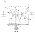
- Each resonator 53a, 53b is conductive and illustratively an X-shape and the asymmetric X-shape as illustrated in FIG. 2 . It is understood that an X-shape may include both symmetric X-shapes and assymetric X-shapes. Of course, there may be any number of resonators and arms. Additionally, each resonator 53a, 53b may have a different shape.
- X-shaped conductive resonators 53a, 53b may force a higher order polynomial response by increasing the number of passband ripples, as will be appreciated by those skilled in the art.
- the impedance response of the X-shaped conductive resonators 53a, 53b, and, in turn, the antenna frequency response may be adjusted by the changing the overall length a+b of each the X-shaped conductive resonators and the spread angle ⁇ between the arms.
- Spread angle ⁇ adjusts the Q factor of the X-shaped resonators 53a, 53b .
- the length a+b adjusts the resonant frequency of each resonator 53a, 53b ; in other words a bigger X-shaped conductive resonator has self resonance at lower frequency and a physically smaller one resonates at a higher frequency.
- a preferred length for a+b may be that length which results a half wave resonance from X-shaped resonator arm tip to arm tip.
- the ratio of a divided by b e.g. a/b , adjusts the degree to which each asymmetric X-shaped conductive resonator electrically couples with to the antenna assembly 30 .
- a larger ratio of a/b provides a more asymmetric X-shaped conductive resonator 53a, 53b m which may couple less into the antenna assembly 30 electrically, reducing antenna assembly 30 passband ripple.
- a smaller ratio of a/b means more a symmetric X-shaped conductive resonator 53a, 53b which may couple more into the antenna assembly 30 to increase bandwidth.
- the X-shaped resonators 53a, 53b allow a tradeoff between antenna assembly 30 passband ripple amplitude and overall bandwidth of the antenna assembly 30 . Higher ripple amplitude means more bandwidth.
- Each resonator 53a, 53b is in effect one or more resonant circuits in parallel with the antenna.
- Each X-shaped conductive resonator 53a, 53b may typically carry a sinusoidal current distribution. Connecting the X-shaped conductive resonators 53a, 53b in parallel at the first and second feed lines 41a, 41b increases the antenna system 30 polynomial tuning order. A bandwidth increase of 2 to 4 fold, or even more, may be obtained when the X-shaped resonators 53a, 53b are included in the antenna assembly 30 , depending on the trades of selected ripple level, spread angle ⁇ , and X-shaped conductive resonators 53a, 53b arm length.
- the first and second feed lines 41a, 41b may be fed by a coaxial antenna feed line 61 from the wireless communications circuitry 21 .
- An outer conductor 63 of the coaxial antenna feed line 61 is coupled to the ground plane 32 , for example, soldered to a via filled ground pad 71 while an inner conductor 62 of the coaxial antenna feed line is coupled to a common transmission line 64 .
- the common transmission line 64 continues to the parallel junction 69 with the first and second feed lines 41a, 41b .
- RF power divides at the parallel junction 69 to feed the first and second feed lines 41a , 41b .
- the power division may be equal in most embodiments, but may be unequal if needed to further synthesize patterns shape, overcome transmission line losses etc.
- Positioning transformers the first and second feed lines 41a , 41b can adjust the branched-off impedances at the parallel junction 69 and, in turn, that power division ratio.
- the antenna assembly 30 may be used independently from the illustrated onboard wireless communications circuitry 21 .
- the antenna assembly 30 may optionally include a cover layer 48 over the upper surface of the substrate and covering the first and second feed capacitive points 37a, 37b and conductive bucking vias 46a, 46b ( FIG. 3 ).
- the cover layer 48 may be a substantially nonconductive material and have a relative permittivity ⁇ r within ⁇ 20%, and more preferably, equal to, the relative permeability ⁇ r . In other words ⁇ r ⁇ ⁇ r in the cover layer 48 .
- the characteristic impedance of the cover layer 48 is then nearly that of free space for all values of ⁇ r ⁇ ⁇ r .
- the further advantage of an ⁇ r ⁇ ⁇ r cover layer 48 with Z cover ⁇ 377 ohms is that the cover layer is then reflection-less for all values of the thicknesses of the cover layer.
- the substrate 31 may likewise have properties of a relative permittivity and a relative permittivity within ⁇ 20% of each other, and more particularly, ⁇ r ⁇ ⁇ r , and which may provide a similarly miniaturized substrate with time delay, group delay, and differential phase that is more constant over frequency.
- Example ⁇ r ⁇ ⁇ r cover layer materials 48 may include light nickel zinc ferrites such as mix 68 by Fair Rite of Wallkill, New York, or material M5 by National Magnetics Group - TCI Ceramics of Bethlehem, Pennsylvania. Of course mixes of magnetic and dielectric powders may be used with binders to achieve a cover layer 48 with a desired value of ⁇ r ⁇ ⁇ r .
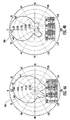
- Traces 504 , 506 are the realized gain data in units of dBi. Realized gain includes material losses and mismatch losses.
- the radiation pattern was righted so peak pattern amplitude occurred nearly exactly at patch plane perpendicular when the additional feed line 41a, 41b was included.
- An additional feed line e.g., one of the feed lines 41a, 41b , may be added to a patch antenna at little to no cost increase at the same time as the first feed line is manufactured.
- a method aspect is directed to a method of making the antenna assembly 30 .
- the method includes forming an electrically conductive patch antenna element 33 on a substrate 31 and spaced from an electrically conductive layer defining a ground plane 32 .
- the electrically conductive patch antenna element 33 is formed to have a symmetric axis 34 dividing the electrically conductive patch antenna element into first and second symmetric areas 35a, 35b .
- the electrically conductive patch antenna element 33 is formed to have first and second feed openings 36a, 36b in the first and second symmetric areas 35a, 35b , respectively.
- the method includes forming first and second feed pads in the first and second feed openings, respectively, defining first and second capacitive feed points 37a, 37b .
- the method also includes forming first and second feed lines 41a, 41b extending through the substrate 31 and respectively coupling the first and second feed pads 37a, 37b to wireless communications circuitry 21 .
- the method also includes forming a plurality of spaced apart conductive shielding vias 42 coupled to the ground plane 32 and extending through the substrate 31 surrounding the electrically conductive patch antenna element 33 .
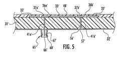
- the antenna assembly 30' includes a substrate 31' and an electrically conductive layer defining a ground plane 32' carried by the substrate.
- the antenna assembly 30' also includes an electrically conductive patch antenna element 33' carried by the substrate 31' and spaced from the ground plane 32' .
- the antenna assembly 30' may not include a multilayer type printed circuit board, and therefore may be more economic to manufacture than the antenna assembly 30 embodiment described above.
- the electrically conductive patch antenna element 33' has a symmetric axis 34' dividing the electrically conductive patch antenna element into first and second symmetric areas 35a', 35b' .
- the electrically conductive patch antenna element 33' has first and second feed openings 36a', 36b' in the first and second symmetric areas 35a', 35b' , respectively.
- First and second feed pads are in the first and second feed openings, respectively, defining first and second capacitive feed points 37a', 37b' .
- the antenna assembly 30' also includes first and second feed lines 41a', 41b' extending through the substrate 31' .
- one of the first and second feed lines 41a' couples a respective one of the first and second feed pads 36a' to the wireless communications circuitry 21' (i.e., a drive feed line) and the other of the first and second feed lines 41b' is electrically floating.
- the ground plane 32' has an opening 56' therein.
- the substrate 31' also has a recess 57' therein aligned with the opening 56' in the ground plane 32' .
- the recess 57' may be conically shaped, for example.
- the electrically floating feed line 41b' illustratively extends downwardly from the electrically conductive patch antenna element 33' to the recess 57'.
- the electrically floating feed line 41b' may be considered a parasitic feed line and may provide useful radiation pattern symmetry without a microstrip power divider or an additional printed circuit board layer to drive it.
- the electrically floating feed line 41b' makes electrical contact with first and second capacitive feed points 37a', 37b' at an upper end thereof and makes no electrical contact with the ground plane 32' at a lower end thereof.
- An open circuit exists at the lower end of the electrically floating or parasitic feed line 41b' due to the conically shaped recess 57' and opening 56' in the ground plane 32 '.
- the capacitive feed point 37b' adjacent the electrically floating feed line 41b' may have the same dimensions as the other capacitive feed point 37a'.
- the first and second capacitive feed points 37a', 37b' may have different sizes.
- the electrically floating feed line 41b' receives electric current from the electrically conductive patch antenna element 33' .
- the electric current on the electrically floating feed line 41b' causes monopole-like radiation, which counteracts radiation by the drive feed line 41a'. Radiation from the drive feed line 41a' squints the radiation pattern off broadside in the direction of the drive feed line, while radiation from the electrically floating feed line 41b' squints the radiation pattern in the direction of the electrically floating feed line. Combined radiation from the first and second feed lines 41a' 41b' (i.e., drive and electrically floating feed lines) steers the antenna radiation pattern to broadside or nearly so.
- E field plane cuts are E field plane cuts.
- E plane and H plane is a shorthand to describe linearly polarized antenna physical orientations and for the antenna assembly 30' .
- Both the first and second feed lines 41a', 41b' physically lie in that E field plane.
- Traces 604, 606 are the simulated realized gain data in units of dBi. Realized gain includes material losses and mismatch losses.
- the pattern peak with the electrically floating feed line 41b' was only 8° from patch plane broadside and only 0.3 dB lower in realized gain at patch plane normal.
- the electrically floating feed line 41b' pattern improvements occurred without having to configure a power divider other apparatus to drive the electrically floating feed line. Further, since at least one probe, the first feed line 41' , is being implemented, adding the electrically floating feed line 41b' to a design can be negligible in cost.
- Table 1 further describes the characteristics of the example embodiment antenna assembly 30' from which the radiation patterns were obtained: Table 1: Antenna Assembly 30' Example Parameters Antenna type Square microstrip patch, 1 ⁇ 2 ⁇ edges nominal, probe driven. Special feature Electrically floating feed line 41b' , driven by patch through a capacitor pad Application Earth station antenna for AO-50 and AO-78 satellites Construction method Suspended microstrip (very thin PWB provides patch element atop a thick foam substrate) Analysis method Finite element simulation using Ansys HFSS, plus validation with a physical prototype.
- First feed line 41a location (driving probe location 2.339 inches from radiating edge Electrically floating feed line 41b' location Image point, 2.339 inches from opposite radiating edge X-shaped conductive resonators 53a, 53b Not used in this example.
- Top cover 49 Not used in this example.
- First and second capacitive feed points 37a' , 37b' (capacitor pad size) 0.654 x 0.654 inches Matching capacitor gap, around first and second capacitive feed points 37a', 37b' 0.050 inches Matching capacitor electrical value, first and second capacitive feed points 37a', 37b' About 3.74 picofarads. This capacitor bucks the feed probe inductance and double tunes the antenna.
- FIG. 8 is a graph of the swept gain analyzed for the Table 1 antenna assembly 30' .
- Trace 704 is the realized gain response over frequency.
- Two peaks 706, 708 can be seen as well as a dip 710 .
- the difference between the peaks 706, 708 and the dip 701 define a response ripple that is small, less than 1 decibel.
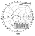
- the Smith Chart of FIG. 9 is the driven (not floating) feed line 41a' impedance at the ground plane penetration.
- Trace 804 is a sweep of the impedance data points in frequency.
- the Smith Chart of FIG. 12 presents the reflection coefficient S 11 .
- Crossover 806 represents the two gain peaks 706, 708 from the graph of FIG. 8 . Moving the driven (not floating) feed line 41a' towards the patch edge moves the trace locus 804 to the right, and moving the driven (not floating) feed line 41a' towards the patch center moves the trace locus 804 to the left in the Smith Chart of FIG. 9 .
- Marker data 808 shows the vector impedance at specific frequencies after being normalized to 50 Ohms.
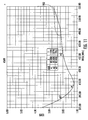
- the graph of FIG. 10 shows a simulated voltage standing wave ratio (VSWR) trace 902 as measured at the driven (not floating) feed line 41a' in a 50 Ohm system.
- the simulation was based upon a 2.17 inch thickness polystyrene foam sheet for the antenna substrate 31' .
- the bandwidth could be further extended with a thicker substrate material, for example.
- the Table 1 example and data thereof should not be construed as limiting the scope of possible antenna embodiments.
- Including one or more electrically floating feed lines is beneficial for most varieties of patch antennas, including patch elements of many shapes, including circular or polygonal shapes, and for stacked patch antennas.
- a plurality of electrically floating feed lines can be used to improve radiation from dual polarization patch antennas, such as antennas providing simultaneous dual linear polarization and or simultaneous dual circular polarization.
- spaced apart conductive shielding vias 42' are coupled to the ground plane 32' and extend through the substrate 31' surrounding the electrically conductive patch antenna element 33' .
- a coaxial connector 65' is carried by the bottom of the substrate 31' .
- the ground plane 22' has an opening 66' therein to allow passage of the first feed line 41a' , or drive feed line, to pass therethrough for coupling with an inner conductor of a coaxial cable, for example.
- the body 67' of the coaxial connector 65' which illustratively includes threads 68' for coupling to a mating coaxial cable connector for example, is coupled to the ground plane 32' and also couples the outer conductor of the coaxial cable to the ground plane.
- the antenna assembly 30 may be used independently from the illustrated onboard wireless communications circuitry 21 .
- a method aspect is directed to a method of making the antenna assembly 30' .
- the method includes forming an electrically conductive patch antenna element 33' on a substrate 31' and spaced from an electrically conductive layer defining a ground plane 32' .
- the electrically conductive patch antenna element 33' is formed to have a symmetric axis 34' dividing the electrically conductive patch antenna element into first and second symmetric areas 35a', 35b' .
- the electrically conductive patch antenna element 33' is also formed to have first and second feed openings 36a', 36b' in the first and second symmetric areas 35a', 35b' , respectively.
- the method includes forming first and second feed pads in the first and second feed openings 36a', 36b' , respectively, defining first and second capacitive feed points 37a', 37b' .
- the method also includes forming first and second feed lines 41a', 41b' extending through the substrate 31' .
- One of the first and second feed lines 41a' couples a respective one of the first and second capacitive feed points 37a' to wireless communications circuitry 21' and another of the first and second feed lines 41b' is electrically floating.
- the method also includes forming spaced apart conductive shielding vias 42' coupled to the ground plane 32' and extending through the substrate 31' surrounding the electrically conductive patch antenna element 33' .
- a common substrate 31" carries four electrically conductive patch antenna elements 33", 133", 233", 333", each being symmetrical and with corresponding first and second capacitive feed points and first and second feed lines as described above with respect to FIGS. 3-5 (i.e., each having a drive feed line 41a", 141a”, 241a", 341a” and an electrically floating feed line 41b", 141b", 241b", 341b” ).
- the array advantageously increases the radiation pattern symmetry by mitigating undesired feed probe radiation.
- the array 30" causes symmetric, broadside radiation.
- the electrically conductive patch antenna elements 33", 133", 233", 333" are alternately “clocked” so half of the electrically conductive patch antenna elements are rotated 180 degrees mechanically with respect to the others.
- the clocking enhances radiation pattern symmetry because if individual element radiation patterns are squinted off broadside/plane normal, the alternate clocked elements will radiate in the other direction cancelling the squint.
- the mechanically clocked elements are fed with an additional 180 degrees of electrical phase delay using an added length from the microstrip branch from the radial power divider, or in other words, from different length meander lines 52", 152", 252", 352".
- the embodiments described herein may, for example, advantageously mitigate unwanted radiation from microstrip patch antenna feed probes, increase patch antenna radiation bandwidth, reduce patch antenna size, and improve patch antenna radiation pattern symmetry.
- the antenna assembly may be a circular polarization patch antenna assembly, as well as a dual channel linear polarization antenna assembly, and a dual channel circular polarization assembly.
Landscapes
- Physics & Mathematics (AREA)
- Electromagnetism (AREA)
- Variable-Direction Aerials And Aerial Arrays (AREA)
- Waveguide Aerials (AREA)
- Details Of Aerials (AREA)
Applications Claiming Priority (1)
| Application Number | Priority Date | Filing Date | Title |
|---|---|---|---|
| US14/640,736 US9825357B2 (en) | 2015-03-06 | 2015-03-06 | Electronic device including patch antenna assembly having capacitive feed points and spaced apart conductive shielding vias and related methods |
Publications (2)
| Publication Number | Publication Date |
|---|---|
| EP3065218A1 true EP3065218A1 (fr) | 2016-09-07 |
| EP3065218B1 EP3065218B1 (fr) | 2020-04-15 |
Family
ID=55435930
Family Applications (1)
| Application Number | Title | Priority Date | Filing Date |
|---|---|---|---|
| EP16000446.1A Active EP3065218B1 (fr) | 2015-03-06 | 2016-02-24 | Dispositif électronique comprenant un ensemble d'antenne à plaque ayant des points d'alimentation capacitive et des trous d'interconnexion de blindage de conducteurs espacés et procédés associés |
Country Status (6)
| Country | Link |
|---|---|
| US (1) | US9825357B2 (fr) |
| EP (1) | EP3065218B1 (fr) |
| KR (1) | KR101854517B1 (fr) |
| CN (1) | CN105938940B (fr) |
| CA (1) | CA2921513C (fr) |
| TW (1) | TWI623150B (fr) |
Cited By (5)
| Publication number | Priority date | Publication date | Assignee | Title |
|---|---|---|---|---|
| JP2019068345A (ja) * | 2017-10-04 | 2019-04-25 | 株式会社ヨコオ | アンテナ装置 |
| EP3624263A1 (fr) * | 2018-09-12 | 2020-03-18 | u-blox AG | Antenne à plaque multibandes |
| CN112913080A (zh) * | 2018-09-12 | 2021-06-04 | 阿莫技术有限公司 | 贴片天线 |
| CN114284711A (zh) * | 2021-12-27 | 2022-04-05 | 湖北三江航天险峰电子信息有限公司 | 一种圆极化天线元 |
| WO2022096119A1 (fr) * | 2020-11-06 | 2022-05-12 | Huawei Technologies Co., Ltd. | Élément d'antenne et réseau d'antennes comprenant de tels éléments d'antenne |
Families Citing this family (40)
| Publication number | Priority date | Publication date | Assignee | Title |
|---|---|---|---|---|
| WO2017019738A1 (fr) * | 2015-07-30 | 2017-02-02 | Laird Technologies, Inc. | Blindages contre les interférences électromagnétiques et procédés associés |
| US10333222B2 (en) * | 2016-04-11 | 2019-06-25 | Electronics And Telecommunications Research Institute | Method of improving bandwidth of antenna using transmission line stub |
| US10418706B1 (en) * | 2016-07-19 | 2019-09-17 | Southern Methodist University | Circular polarized microstrip antenna using a single feed |
| US10044111B2 (en) * | 2016-10-10 | 2018-08-07 | Phazr, Inc. | Wideband dual-polarized patch antenna |
| TWI652790B (zh) | 2016-10-19 | 2019-03-01 | Upi Semiconductor Corp. | 瞬間電壓抑制器裝置 |
| US10079429B1 (en) * | 2017-03-08 | 2018-09-18 | Nxp B.V. | Wireless device antenna |
| NO345389B1 (en) | 2017-03-15 | 2021-01-11 | Norbit Its | Patch antenna feed |
| KR102352592B1 (ko) * | 2017-07-13 | 2022-01-19 | 삼성전자주식회사 | 어레이 안테나를 포함하는 전자 장치 |
| US11888218B2 (en) * | 2017-07-26 | 2024-01-30 | California Institute Of Technology | Method and apparatus for reducing surface waves in printed antennas |
| WO2019076928A1 (fr) | 2017-10-17 | 2019-04-25 | Sony Mobile Communications Inc. | Antenne patch supportée par une cavité |
| WO2019086486A1 (fr) * | 2017-10-30 | 2019-05-09 | Fractus Antennas, S.L. | Dispositifs dotés de systèmes rayonnants à proximité de corps conducteurs |
| US10720707B2 (en) * | 2017-11-08 | 2020-07-21 | Qorvo Us, Inc. | Reconfigurable patch antenna and phased array |
| WO2019116756A1 (fr) * | 2017-12-14 | 2019-06-20 | 株式会社村田製作所 | Module antennes et dispositif d'antenne |
| KR102445368B1 (ko) * | 2017-12-14 | 2022-09-20 | 현대자동차주식회사 | 안테나 장치 및 차량 |
| CN111433976A (zh) * | 2017-12-14 | 2020-07-17 | 株式会社村田制作所 | 天线装置、天线模块和无线装置 |
| US10763584B2 (en) * | 2018-01-17 | 2020-09-01 | Nxp B.V. | Conductive plane antenna |
| CN111052504B (zh) * | 2018-05-09 | 2022-07-22 | 华为技术有限公司 | 毫米波天线阵元、阵列天线及通信产品 |
| US11677144B1 (en) * | 2018-06-26 | 2023-06-13 | Orbcomm Inc. | Multiple beam phased array antenna system for mobile satellite communications |
| KR102158304B1 (ko) * | 2018-08-30 | 2020-09-22 | 동우 화인켐 주식회사 | 고주파용 필름 전송 선로, 이를 포함하는 안테나 및 안테나가 결합된 화상 표시 장치 |
| JP6741189B1 (ja) * | 2018-09-07 | 2020-08-19 | 株式会社村田製作所 | アンテナ素子、アンテナモジュールおよび通信装置 |
| CN109244659A (zh) * | 2018-11-08 | 2019-01-18 | 上海圣丹纳无线科技有限公司 | 一种基片集成波导双极化天线 |
| KR102137198B1 (ko) * | 2019-03-18 | 2020-07-24 | 삼성전기주식회사 | 안테나 장치, 안테나 모듈 및 그에 배치되는 칩 패치 안테나 |
| US11158948B2 (en) * | 2019-03-20 | 2021-10-26 | Samsung Electro-Mechanics Co., Ltd. | Antenna apparatus |
| CN111934086B (zh) * | 2019-05-13 | 2022-11-22 | 启碁科技股份有限公司 | 天线结构 |
| KR102639685B1 (ko) * | 2019-05-17 | 2024-02-23 | 삼성전자주식회사 | 안테나 모듈을 포함하는 전자 장치 |
| US10957978B2 (en) * | 2019-06-28 | 2021-03-23 | Apple Inc. | Electronic devices having multi-frequency ultra-wideband antennas |
| US11522300B2 (en) * | 2019-06-28 | 2022-12-06 | Corning Incorporated | Integral 5G antenna structure |
| CN111129723B (zh) * | 2019-11-29 | 2022-04-08 | 北京遥测技术研究所 | 一种宽频带双极化阵列天线单元 |
| KR102320427B1 (ko) * | 2020-07-07 | 2021-11-03 | (주)드림텍 | 회로 기판 |
| CN112510362B (zh) * | 2020-09-25 | 2025-07-18 | 深圳迈睿智能科技有限公司 | 反相双馈电式微波探测模块 |
| CN112736423B (zh) * | 2020-12-10 | 2023-03-21 | 重庆大学 | 一种紧凑型低剖面差分滤波微带贴片天线 |
| CN112751182A (zh) * | 2020-12-28 | 2021-05-04 | Oppo广东移动通信有限公司 | 天线组件及电子设备 |
| US12009915B2 (en) | 2021-01-29 | 2024-06-11 | Eagle Technology, Llc | Compact receiver system with antijam and antispoof capability |
| US11502414B2 (en) | 2021-01-29 | 2022-11-15 | Eagle Technology, Llc | Microstrip patch antenna system having adjustable radiation pattern shapes and related method |
| US11742822B2 (en) * | 2021-04-12 | 2023-08-29 | AchernarTek Inc. | Antenna structure and antenna array |
| CN116093591B (zh) * | 2021-11-05 | 2026-04-28 | 华为终端有限公司 | 天线装置及终端设备 |
| CN114400442B (zh) * | 2022-03-25 | 2022-05-31 | 成都天锐星通科技有限公司 | 双圆极化天线单元和双圆极化阵面天线 |
| CN115548703B (zh) * | 2022-09-28 | 2023-09-22 | 安徽大学 | 一种相位可控双频圆极化天线 |
| US11973530B1 (en) | 2023-04-19 | 2024-04-30 | SomeWear Labs, Inc. | Low latency off-grid communication system with network optimization and low energy signal transmission capabilities |
| US12394907B2 (en) * | 2023-04-21 | 2025-08-19 | Auden Techno Corp. | Antenna array |
Citations (3)
| Publication number | Priority date | Publication date | Assignee | Title |
|---|---|---|---|---|
| US5515057A (en) | 1994-09-06 | 1996-05-07 | Trimble Navigation Limited | GPS receiver with N-point symmetrical feed double-frequency patch antenna |
| WO1999059221A1 (fr) * | 1998-05-08 | 1999-11-18 | Northrop Grumman Corporation | Antenne a plaque a plaque de terre petite au plan electrique, dans laquelle des tenons peripheriques non alimentes sont utilises |
| WO2013149347A1 (fr) * | 2012-04-05 | 2013-10-10 | Tallysman Wireless Inc. | Antenne microbande à couplage capacitif |
Family Cites Families (14)
| Publication number | Priority date | Publication date | Assignee | Title |
|---|---|---|---|---|
| US3921177A (en) | 1973-04-17 | 1975-11-18 | Ball Brothers Res Corp | Microstrip antenna structures and arrays |
| SE9802883L (sv) * | 1998-08-28 | 2000-02-29 | Ericsson Telefon Ab L M | Antennanordning |
| WO2003034545A1 (fr) | 2001-10-16 | 2003-04-24 | Fractus, S.A. | Antenne a plaque microruban multifrequence avec elements couples non alimentes |
| US6882316B2 (en) | 2002-01-23 | 2005-04-19 | Actiontec Electronics, Inc. | DC inductive shorted patch antenna |
| US7084815B2 (en) | 2004-03-22 | 2006-08-01 | Motorola, Inc. | Differential-fed stacked patch antenna |
| US7209080B2 (en) | 2004-07-01 | 2007-04-24 | Raytheon Co. | Multiple-port patch antenna |
| CN101103491B (zh) * | 2005-11-14 | 2012-01-11 | 安立股份有限公司 | 线性极化天线及采用其的雷达设备 |
| CN101038984A (zh) * | 2007-05-10 | 2007-09-19 | 北京航空航天大学 | 一种小型化的gps微带贴片天线的设计 |
| CN101789538B (zh) * | 2009-01-22 | 2011-06-29 | 深圳市华信天线技术有限公司 | 一种多频贴片天线装置 |
| CN102714357B (zh) * | 2010-01-27 | 2015-05-27 | 株式会社村田制作所 | 宽带天线 |
| JP5408166B2 (ja) * | 2011-03-23 | 2014-02-05 | 株式会社村田製作所 | アンテナ装置 |
| TWI518991B (zh) | 2013-02-08 | 2016-01-21 | 巽晨國際股份有限公司 | Integrated antenna and integrated circuit components of the shielding module |
| US20140266959A1 (en) * | 2013-03-15 | 2014-09-18 | City University Of Hong Kong | Patch antenna |
| CN103825084B (zh) * | 2014-02-25 | 2016-03-02 | 东南大学 | 一种适用于无线局域网的2.4/5GHz双频全向天线 |
-
2015
- 2015-03-06 US US14/640,736 patent/US9825357B2/en active Active
-
2016
- 2016-02-22 CA CA2921513A patent/CA2921513C/fr active Active
- 2016-02-24 EP EP16000446.1A patent/EP3065218B1/fr active Active
- 2016-03-02 CN CN201610118034.XA patent/CN105938940B/zh not_active Expired - Fee Related
- 2016-03-04 TW TW105106786A patent/TWI623150B/zh not_active IP Right Cessation
- 2016-03-04 KR KR1020160026266A patent/KR101854517B1/ko not_active Expired - Fee Related
Patent Citations (4)
| Publication number | Priority date | Publication date | Assignee | Title |
|---|---|---|---|---|
| US5515057A (en) | 1994-09-06 | 1996-05-07 | Trimble Navigation Limited | GPS receiver with N-point symmetrical feed double-frequency patch antenna |
| WO1999059221A1 (fr) * | 1998-05-08 | 1999-11-18 | Northrop Grumman Corporation | Antenne a plaque a plaque de terre petite au plan electrique, dans laquelle des tenons peripheriques non alimentes sont utilises |
| US6181279B1 (en) | 1998-05-08 | 2001-01-30 | Northrop Grumman Corporation | Patch antenna with an electrically small ground plate using peripheral parasitic stubs |
| WO2013149347A1 (fr) * | 2012-04-05 | 2013-10-10 | Tallysman Wireless Inc. | Antenne microbande à couplage capacitif |
Cited By (9)
| Publication number | Priority date | Publication date | Assignee | Title |
|---|---|---|---|---|
| JP2019068345A (ja) * | 2017-10-04 | 2019-04-25 | 株式会社ヨコオ | アンテナ装置 |
| EP3624263A1 (fr) * | 2018-09-12 | 2020-03-18 | u-blox AG | Antenne à plaque multibandes |
| CN112913080A (zh) * | 2018-09-12 | 2021-06-04 | 阿莫技术有限公司 | 贴片天线 |
| EP3852196A4 (fr) * | 2018-09-12 | 2022-06-22 | Amotech Co., Ltd. | Antenne à plaque |
| US11387555B2 (en) | 2018-09-12 | 2022-07-12 | U-Blox Ag | Multiband patch antenna |
| WO2022096119A1 (fr) * | 2020-11-06 | 2022-05-12 | Huawei Technologies Co., Ltd. | Élément d'antenne et réseau d'antennes comprenant de tels éléments d'antenne |
| US12603433B2 (en) | 2020-11-06 | 2026-04-14 | Huawei Technologies Co., Ltd. | Antenna element and antenna array comprising such antenna elements |
| CN114284711A (zh) * | 2021-12-27 | 2022-04-05 | 湖北三江航天险峰电子信息有限公司 | 一种圆极化天线元 |
| CN114284711B (zh) * | 2021-12-27 | 2023-07-04 | 湖北三江航天险峰电子信息有限公司 | 一种圆极化天线元 |
Also Published As
| Publication number | Publication date |
|---|---|
| CN105938940A (zh) | 2016-09-14 |
| US9825357B2 (en) | 2017-11-21 |
| CN105938940B (zh) | 2018-08-31 |
| KR101854517B1 (ko) | 2018-05-03 |
| TW201637285A (zh) | 2016-10-16 |
| TWI623150B (zh) | 2018-05-01 |
| US20160261039A1 (en) | 2016-09-08 |
| CA2921513C (fr) | 2018-02-20 |
| KR20160108225A (ko) | 2016-09-19 |
| EP3065218B1 (fr) | 2020-04-15 |
| CA2921513A1 (fr) | 2016-09-06 |
Similar Documents
| Publication | Publication Date | Title |
|---|---|---|
| EP3065218B1 (fr) | Dispositif électronique comprenant un ensemble d'antenne à plaque ayant des points d'alimentation capacitive et des trous d'interconnexion de blindage de conducteurs espacés et procédés associés | |
| US11431087B2 (en) | Wideband, low profile, small area, circular polarized UHF antenna | |
| US10854994B2 (en) | Broadband phased array antenna system with hybrid radiating elements | |
| US9865928B2 (en) | Dual-polarized antenna | |
| JP6579589B2 (ja) | 三偏波の信号用のアンテナ素子 | |
| US8558747B2 (en) | Broadband clover leaf dipole panel antenna | |
| US10886620B2 (en) | Antenna | |
| CN110931965B (zh) | 双频天线和飞行器 | |
| WO2016100291A1 (fr) | Systèmes d'antenne comprenant des pièces rectangulaires annulaires couplées par proximité | |
| US9819086B2 (en) | Dual-band inverted-F antenna with multiple wave traps for wireless electronic devices | |
| CN105720357B (zh) | 一种圆极化天线 | |
| Cahyasiwi et al. | Switchable slant polarization filtering antenna using two inverted resonator structures for 5G application | |
| CN107078393A (zh) | 用于无线电子设备的双频带多层偶极子天线 | |
| KR101727489B1 (ko) | 직교 편파된 음의 공진 crlh 패치 안테나 | |
| EP1798816A1 (fr) | Réseau d'antennes à fente et à double polarisations avec plaque capacitive de couplage entre les éléments et procédés associés | |
| CN210111029U (zh) | 一种双频天线及飞行器 | |
| US20170194701A1 (en) | Broadband omnidirectional dipole antenna systems | |
| Rasheduzzaman et al. | Performance analysis of a hexagonal microstrip antenna for S-band spectrum using HFSS | |
| RU2776603C1 (ru) | Печатная двухдиапазонная дипольная антенна | |
| Tabaiya et al. | Slotted Rectangular Microstrip Patch Antenna for 2.4 GHz Applications | |
| Panahi | Reconfigurable monopole antennas with circular polarization | |
| RU131242U1 (ru) | Антенный фрагмент фазированной антенной решетки с управляемой поляризацией | |
| Alekseitsev et al. | The modified dual-frequency dipole antenna | |
| EP4020710A1 (fr) | Antenne à polarisation circulaire | |
| CN121484477A (zh) | 一种贴片天线及车辆 |
Legal Events
| Date | Code | Title | Description |
|---|---|---|---|
| PUAI | Public reference made under article 153(3) epc to a published international application that has entered the european phase |
Free format text: ORIGINAL CODE: 0009012 |
|
| 17P | Request for examination filed |
Effective date: 20160224 |
|
| AK | Designated contracting states |
Kind code of ref document: A1 Designated state(s): AL AT BE BG CH CY CZ DE DK EE ES FI FR GB GR HR HU IE IS IT LI LT LU LV MC MK MT NL NO PL PT RO RS SE SI SK SM TR |
|
| AX | Request for extension of the european patent |
Extension state: BA ME |
|
| STAA | Information on the status of an ep patent application or granted ep patent |
Free format text: STATUS: EXAMINATION IS IN PROGRESS |
|
| 17Q | First examination report despatched |
Effective date: 20190314 |
|
| GRAP | Despatch of communication of intention to grant a patent |
Free format text: ORIGINAL CODE: EPIDOSNIGR1 |
|
| STAA | Information on the status of an ep patent application or granted ep patent |
Free format text: STATUS: GRANT OF PATENT IS INTENDED |
|
| INTG | Intention to grant announced |
Effective date: 20191119 |
|
| GRAS | Grant fee paid |
Free format text: ORIGINAL CODE: EPIDOSNIGR3 |
|
| GRAA | (expected) grant |
Free format text: ORIGINAL CODE: 0009210 |
|
| STAA | Information on the status of an ep patent application or granted ep patent |
Free format text: STATUS: THE PATENT HAS BEEN GRANTED |
|
| AK | Designated contracting states |
Kind code of ref document: B1 Designated state(s): AL AT BE BG CH CY CZ DE DK EE ES FI FR GB GR HR HU IE IS IT LI LT LU LV MC MK MT NL NO PL PT RO RS SE SI SK SM TR |
|
| REG | Reference to a national code |
Ref country code: CH Ref legal event code: EP |
|
| REG | Reference to a national code |
Ref country code: DE Ref legal event code: R096 Ref document number: 602016033901 Country of ref document: DE |
|
| REG | Reference to a national code |
Ref country code: IE Ref legal event code: FG4D |
|
| REG | Reference to a national code |
Ref country code: AT Ref legal event code: REF Ref document number: 1258375 Country of ref document: AT Kind code of ref document: T Effective date: 20200515 |
|
| REG | Reference to a national code |
Ref country code: NL Ref legal event code: MP Effective date: 20200415 |
|
| REG | Reference to a national code |
Ref country code: LT Ref legal event code: MG4D |
|
| PG25 | Lapsed in a contracting state [announced via postgrant information from national office to epo] |
Ref country code: GR Free format text: LAPSE BECAUSE OF FAILURE TO SUBMIT A TRANSLATION OF THE DESCRIPTION OR TO PAY THE FEE WITHIN THE PRESCRIBED TIME-LIMIT Effective date: 20200716 Ref country code: IS Free format text: LAPSE BECAUSE OF FAILURE TO SUBMIT A TRANSLATION OF THE DESCRIPTION OR TO PAY THE FEE WITHIN THE PRESCRIBED TIME-LIMIT Effective date: 20200815 Ref country code: SE Free format text: LAPSE BECAUSE OF FAILURE TO SUBMIT A TRANSLATION OF THE DESCRIPTION OR TO PAY THE FEE WITHIN THE PRESCRIBED TIME-LIMIT Effective date: 20200415 Ref country code: LT Free format text: LAPSE BECAUSE OF FAILURE TO SUBMIT A TRANSLATION OF THE DESCRIPTION OR TO PAY THE FEE WITHIN THE PRESCRIBED TIME-LIMIT Effective date: 20200415 Ref country code: NL Free format text: LAPSE BECAUSE OF FAILURE TO SUBMIT A TRANSLATION OF THE DESCRIPTION OR TO PAY THE FEE WITHIN THE PRESCRIBED TIME-LIMIT Effective date: 20200415 Ref country code: FI Free format text: LAPSE BECAUSE OF FAILURE TO SUBMIT A TRANSLATION OF THE DESCRIPTION OR TO PAY THE FEE WITHIN THE PRESCRIBED TIME-LIMIT Effective date: 20200415 Ref country code: NO Free format text: LAPSE BECAUSE OF FAILURE TO SUBMIT A TRANSLATION OF THE DESCRIPTION OR TO PAY THE FEE WITHIN THE PRESCRIBED TIME-LIMIT Effective date: 20200715 Ref country code: PT Free format text: LAPSE BECAUSE OF FAILURE TO SUBMIT A TRANSLATION OF THE DESCRIPTION OR TO PAY THE FEE WITHIN THE PRESCRIBED TIME-LIMIT Effective date: 20200817 |
|
| REG | Reference to a national code |
Ref country code: AT Ref legal event code: MK05 Ref document number: 1258375 Country of ref document: AT Kind code of ref document: T Effective date: 20200415 |
|
| PG25 | Lapsed in a contracting state [announced via postgrant information from national office to epo] |
Ref country code: LV Free format text: LAPSE BECAUSE OF FAILURE TO SUBMIT A TRANSLATION OF THE DESCRIPTION OR TO PAY THE FEE WITHIN THE PRESCRIBED TIME-LIMIT Effective date: 20200415 Ref country code: RS Free format text: LAPSE BECAUSE OF FAILURE TO SUBMIT A TRANSLATION OF THE DESCRIPTION OR TO PAY THE FEE WITHIN THE PRESCRIBED TIME-LIMIT Effective date: 20200415 Ref country code: HR Free format text: LAPSE BECAUSE OF FAILURE TO SUBMIT A TRANSLATION OF THE DESCRIPTION OR TO PAY THE FEE WITHIN THE PRESCRIBED TIME-LIMIT Effective date: 20200415 Ref country code: BG Free format text: LAPSE BECAUSE OF FAILURE TO SUBMIT A TRANSLATION OF THE DESCRIPTION OR TO PAY THE FEE WITHIN THE PRESCRIBED TIME-LIMIT Effective date: 20200715 |
|
| PG25 | Lapsed in a contracting state [announced via postgrant information from national office to epo] |
Ref country code: AL Free format text: LAPSE BECAUSE OF FAILURE TO SUBMIT A TRANSLATION OF THE DESCRIPTION OR TO PAY THE FEE WITHIN THE PRESCRIBED TIME-LIMIT Effective date: 20200415 |
|
| REG | Reference to a national code |
Ref country code: DE Ref legal event code: R097 Ref document number: 602016033901 Country of ref document: DE |
|
| PG25 | Lapsed in a contracting state [announced via postgrant information from national office to epo] |
Ref country code: ES Free format text: LAPSE BECAUSE OF FAILURE TO SUBMIT A TRANSLATION OF THE DESCRIPTION OR TO PAY THE FEE WITHIN THE PRESCRIBED TIME-LIMIT Effective date: 20200415 Ref country code: CZ Free format text: LAPSE BECAUSE OF FAILURE TO SUBMIT A TRANSLATION OF THE DESCRIPTION OR TO PAY THE FEE WITHIN THE PRESCRIBED TIME-LIMIT Effective date: 20200415 Ref country code: AT Free format text: LAPSE BECAUSE OF FAILURE TO SUBMIT A TRANSLATION OF THE DESCRIPTION OR TO PAY THE FEE WITHIN THE PRESCRIBED TIME-LIMIT Effective date: 20200415 Ref country code: IT Free format text: LAPSE BECAUSE OF FAILURE TO SUBMIT A TRANSLATION OF THE DESCRIPTION OR TO PAY THE FEE WITHIN THE PRESCRIBED TIME-LIMIT Effective date: 20200415 Ref country code: RO Free format text: LAPSE BECAUSE OF FAILURE TO SUBMIT A TRANSLATION OF THE DESCRIPTION OR TO PAY THE FEE WITHIN THE PRESCRIBED TIME-LIMIT Effective date: 20200415 Ref country code: DK Free format text: LAPSE BECAUSE OF FAILURE TO SUBMIT A TRANSLATION OF THE DESCRIPTION OR TO PAY THE FEE WITHIN THE PRESCRIBED TIME-LIMIT Effective date: 20200415 Ref country code: EE Free format text: LAPSE BECAUSE OF FAILURE TO SUBMIT A TRANSLATION OF THE DESCRIPTION OR TO PAY THE FEE WITHIN THE PRESCRIBED TIME-LIMIT Effective date: 20200415 Ref country code: SM Free format text: LAPSE BECAUSE OF FAILURE TO SUBMIT A TRANSLATION OF THE DESCRIPTION OR TO PAY THE FEE WITHIN THE PRESCRIBED TIME-LIMIT Effective date: 20200415 |
|
| PLBE | No opposition filed within time limit |
Free format text: ORIGINAL CODE: 0009261 |
|
| STAA | Information on the status of an ep patent application or granted ep patent |
Free format text: STATUS: NO OPPOSITION FILED WITHIN TIME LIMIT |
|
| PG25 | Lapsed in a contracting state [announced via postgrant information from national office to epo] |
Ref country code: SK Free format text: LAPSE BECAUSE OF FAILURE TO SUBMIT A TRANSLATION OF THE DESCRIPTION OR TO PAY THE FEE WITHIN THE PRESCRIBED TIME-LIMIT Effective date: 20200415 Ref country code: PL Free format text: LAPSE BECAUSE OF FAILURE TO SUBMIT A TRANSLATION OF THE DESCRIPTION OR TO PAY THE FEE WITHIN THE PRESCRIBED TIME-LIMIT Effective date: 20200415 |
|
| 26N | No opposition filed |
Effective date: 20210118 |
|
| PG25 | Lapsed in a contracting state [announced via postgrant information from national office to epo] |
Ref country code: SI Free format text: LAPSE BECAUSE OF FAILURE TO SUBMIT A TRANSLATION OF THE DESCRIPTION OR TO PAY THE FEE WITHIN THE PRESCRIBED TIME-LIMIT Effective date: 20200415 |
|
| PG25 | Lapsed in a contracting state [announced via postgrant information from national office to epo] |
Ref country code: MC Free format text: LAPSE BECAUSE OF FAILURE TO SUBMIT A TRANSLATION OF THE DESCRIPTION OR TO PAY THE FEE WITHIN THE PRESCRIBED TIME-LIMIT Effective date: 20200415 |
|
| REG | Reference to a national code |
Ref country code: BE Ref legal event code: MM Effective date: 20210228 |
|
| PG25 | Lapsed in a contracting state [announced via postgrant information from national office to epo] |
Ref country code: LU Free format text: LAPSE BECAUSE OF NON-PAYMENT OF DUE FEES Effective date: 20210224 Ref country code: LI Free format text: LAPSE BECAUSE OF NON-PAYMENT OF DUE FEES Effective date: 20210228 Ref country code: CH Free format text: LAPSE BECAUSE OF NON-PAYMENT OF DUE FEES Effective date: 20210228 |
|
| PG25 | Lapsed in a contracting state [announced via postgrant information from national office to epo] |
Ref country code: FR Free format text: LAPSE BECAUSE OF NON-PAYMENT OF DUE FEES Effective date: 20210228 Ref country code: IE Free format text: LAPSE BECAUSE OF NON-PAYMENT OF DUE FEES Effective date: 20210224 |
|
| PG25 | Lapsed in a contracting state [announced via postgrant information from national office to epo] |
Ref country code: BE Free format text: LAPSE BECAUSE OF NON-PAYMENT OF DUE FEES Effective date: 20210228 |
|
| PG25 | Lapsed in a contracting state [announced via postgrant information from national office to epo] |
Ref country code: HU Free format text: LAPSE BECAUSE OF FAILURE TO SUBMIT A TRANSLATION OF THE DESCRIPTION OR TO PAY THE FEE WITHIN THE PRESCRIBED TIME-LIMIT; INVALID AB INITIO Effective date: 20160224 |
|
| PG25 | Lapsed in a contracting state [announced via postgrant information from national office to epo] |
Ref country code: CY Free format text: LAPSE BECAUSE OF FAILURE TO SUBMIT A TRANSLATION OF THE DESCRIPTION OR TO PAY THE FEE WITHIN THE PRESCRIBED TIME-LIMIT Effective date: 20200415 |
|
| P01 | Opt-out of the competence of the unified patent court (upc) registered |
Effective date: 20230525 |
|
| PG25 | Lapsed in a contracting state [announced via postgrant information from national office to epo] |
Ref country code: MK Free format text: LAPSE BECAUSE OF FAILURE TO SUBMIT A TRANSLATION OF THE DESCRIPTION OR TO PAY THE FEE WITHIN THE PRESCRIBED TIME-LIMIT Effective date: 20200415 |
|
| PG25 | Lapsed in a contracting state [announced via postgrant information from national office to epo] |
Ref country code: TR Free format text: LAPSE BECAUSE OF FAILURE TO SUBMIT A TRANSLATION OF THE DESCRIPTION OR TO PAY THE FEE WITHIN THE PRESCRIBED TIME-LIMIT Effective date: 20200415 |
|
| PG25 | Lapsed in a contracting state [announced via postgrant information from national office to epo] |
Ref country code: MT Free format text: LAPSE BECAUSE OF FAILURE TO SUBMIT A TRANSLATION OF THE DESCRIPTION OR TO PAY THE FEE WITHIN THE PRESCRIBED TIME-LIMIT Effective date: 20200415 |
|
| PGFP | Annual fee paid to national office [announced via postgrant information from national office to epo] |
Ref country code: GB Payment date: 20260227 Year of fee payment: 11 |
|
| PGFP | Annual fee paid to national office [announced via postgrant information from national office to epo] |
Ref country code: DE Payment date: 20260227 Year of fee payment: 11 |