EP3067073A1 - Procédé de formation d'un dispositif médical contenant du graphène - Google Patents
Procédé de formation d'un dispositif médical contenant du graphène Download PDFInfo
- Publication number
- EP3067073A1 EP3067073A1 EP15305351.7A EP15305351A EP3067073A1 EP 3067073 A1 EP3067073 A1 EP 3067073A1 EP 15305351 A EP15305351 A EP 15305351A EP 3067073 A1 EP3067073 A1 EP 3067073A1
- Authority
- EP
- European Patent Office
- Prior art keywords
- graphene film
- graphene
- polymer
- polymer material
- patch
- Prior art date
- Legal status (The legal status is an assumption and is not a legal conclusion. Google has not performed a legal analysis and makes no representation as to the accuracy of the status listed.)
- Withdrawn
Links
- OKTJSMMVPCPJKN-UHFFFAOYSA-N Carbon Chemical compound [C] OKTJSMMVPCPJKN-UHFFFAOYSA-N 0.000 title claims abstract description 164
- 229910021389 graphene Inorganic materials 0.000 title claims abstract description 162
- 238000000034 method Methods 0.000 title claims abstract description 44
- 239000000758 substrate Substances 0.000 claims abstract description 41
- 239000002861 polymer material Substances 0.000 claims abstract description 35
- 238000000151 deposition Methods 0.000 claims abstract description 24
- 230000008021 deposition Effects 0.000 claims abstract description 12
- 239000010410 layer Substances 0.000 claims description 62
- 229920000642 polymer Polymers 0.000 claims description 43
- 239000007943 implant Substances 0.000 claims description 32
- 239000000463 material Substances 0.000 claims description 28
- 206010052428 Wound Diseases 0.000 claims description 19
- 208000027418 Wounds and injury Diseases 0.000 claims description 17
- 229920000052 poly(p-xylylene) Polymers 0.000 claims description 15
- 230000008569 process Effects 0.000 claims description 14
- 230000015572 biosynthetic process Effects 0.000 claims description 8
- 230000032798 delamination Effects 0.000 claims description 6
- 239000000853 adhesive Substances 0.000 claims description 5
- 230000001070 adhesive effect Effects 0.000 claims description 5
- 239000012790 adhesive layer Substances 0.000 claims description 5
- 239000011248 coating agent Substances 0.000 claims description 5
- 238000000576 coating method Methods 0.000 claims description 5
- 230000008878 coupling Effects 0.000 claims description 5
- 238000010168 coupling process Methods 0.000 claims description 5
- 238000005859 coupling reaction Methods 0.000 claims description 5
- 239000007789 gas Substances 0.000 description 17
- RYGMFSIKBFXOCR-UHFFFAOYSA-N Copper Chemical compound [Cu] RYGMFSIKBFXOCR-UHFFFAOYSA-N 0.000 description 11
- 241001465754 Metazoa Species 0.000 description 10
- 230000008901 benefit Effects 0.000 description 8
- 238000005229 chemical vapour deposition Methods 0.000 description 8
- 229910052802 copper Inorganic materials 0.000 description 8
- 239000010949 copper Substances 0.000 description 8
- 238000005530 etching Methods 0.000 description 7
- 239000012071 phase Substances 0.000 description 7
- 238000006243 chemical reaction Methods 0.000 description 6
- 239000011162 core material Substances 0.000 description 6
- VNWKTOKETHGBQD-UHFFFAOYSA-N methane Chemical compound C VNWKTOKETHGBQD-UHFFFAOYSA-N 0.000 description 5
- XKRFYHLGVUSROY-UHFFFAOYSA-N Argon Chemical compound [Ar] XKRFYHLGVUSROY-UHFFFAOYSA-N 0.000 description 4
- PXHVJJICTQNCMI-UHFFFAOYSA-N Nickel Chemical compound [Ni] PXHVJJICTQNCMI-UHFFFAOYSA-N 0.000 description 4
- 239000003814 drug Substances 0.000 description 4
- VRBFTYUMFJWSJY-UHFFFAOYSA-N 28804-46-8 Chemical compound ClC1CC(C=C2)=CC=C2C(Cl)CC2=CC=C1C=C2 VRBFTYUMFJWSJY-UHFFFAOYSA-N 0.000 description 3
- 125000004429 atom Chemical group 0.000 description 3
- 239000011889 copper foil Substances 0.000 description 3
- 230000000638 stimulation Effects 0.000 description 3
- 229910000881 Cu alloy Inorganic materials 0.000 description 2
- KJTLSVCANCCWHF-UHFFFAOYSA-N Ruthenium Chemical compound [Ru] KJTLSVCANCCWHF-UHFFFAOYSA-N 0.000 description 2
- 230000004075 alteration Effects 0.000 description 2
- 229910052786 argon Inorganic materials 0.000 description 2
- 238000000231 atomic layer deposition Methods 0.000 description 2
- 229910052799 carbon Inorganic materials 0.000 description 2
- 125000004432 carbon atom Chemical group C* 0.000 description 2
- 239000003054 catalyst Substances 0.000 description 2
- 229910017052 cobalt Inorganic materials 0.000 description 2
- 239000010941 cobalt Substances 0.000 description 2
- GUTLYIVDDKVIGB-UHFFFAOYSA-N cobalt atom Chemical compound [Co] GUTLYIVDDKVIGB-UHFFFAOYSA-N 0.000 description 2
- 239000004020 conductor Substances 0.000 description 2
- 239000011888 foil Substances 0.000 description 2
- 239000001257 hydrogen Substances 0.000 description 2
- 229910052739 hydrogen Inorganic materials 0.000 description 2
- 125000004435 hydrogen atom Chemical class [H]* 0.000 description 2
- 230000006872 improvement Effects 0.000 description 2
- 238000004519 manufacturing process Methods 0.000 description 2
- 229910052751 metal Inorganic materials 0.000 description 2
- 239000002184 metal Substances 0.000 description 2
- 238000012986 modification Methods 0.000 description 2
- 230000004048 modification Effects 0.000 description 2
- TWNQGVIAIRXVLR-UHFFFAOYSA-N oxo(oxoalumanyloxy)alumane Chemical compound O=[Al]O[Al]=O TWNQGVIAIRXVLR-UHFFFAOYSA-N 0.000 description 2
- 238000005240 physical vapour deposition Methods 0.000 description 2
- 239000002243 precursor Substances 0.000 description 2
- 238000012545 processing Methods 0.000 description 2
- 238000012546 transfer Methods 0.000 description 2
- 230000029663 wound healing Effects 0.000 description 2
- 229910052582 BN Inorganic materials 0.000 description 1
- PZNSFCLAULLKQX-UHFFFAOYSA-N Boron nitride Chemical compound N#B PZNSFCLAULLKQX-UHFFFAOYSA-N 0.000 description 1
- VGGSQFUCUMXWEO-UHFFFAOYSA-N Ethene Chemical compound C=C VGGSQFUCUMXWEO-UHFFFAOYSA-N 0.000 description 1
- 239000005977 Ethylene Substances 0.000 description 1
- 229910003803 Gold(III) chloride Inorganic materials 0.000 description 1
- 229910021578 Iron(III) chloride Inorganic materials 0.000 description 1
- 229910000990 Ni alloy Inorganic materials 0.000 description 1
- GRYLNZFGIOXLOG-UHFFFAOYSA-N Nitric acid Chemical compound O[N+]([O-])=O GRYLNZFGIOXLOG-UHFFFAOYSA-N 0.000 description 1
- 239000004642 Polyimide Substances 0.000 description 1
- 229910000929 Ru alloy Inorganic materials 0.000 description 1
- MCMNRKCIXSYSNV-UHFFFAOYSA-N ZrO2 Inorganic materials O=[Zr]=O MCMNRKCIXSYSNV-UHFFFAOYSA-N 0.000 description 1
- 238000009825 accumulation Methods 0.000 description 1
- 239000002253 acid Substances 0.000 description 1
- HSFWRNGVRCDJHI-UHFFFAOYSA-N alpha-acetylene Natural products C#C HSFWRNGVRCDJHI-UHFFFAOYSA-N 0.000 description 1
- QVGXLLKOCUKJST-UHFFFAOYSA-N atomic oxygen Chemical compound [O] QVGXLLKOCUKJST-UHFFFAOYSA-N 0.000 description 1
- 230000004888 barrier function Effects 0.000 description 1
- 229920000249 biocompatible polymer Polymers 0.000 description 1
- 239000001273 butane Substances 0.000 description 1
- 230000015556 catabolic process Effects 0.000 description 1
- 239000006071 cream Substances 0.000 description 1
- 239000013078 crystal Substances 0.000 description 1
- 238000006731 degradation reaction Methods 0.000 description 1
- 230000000593 degrading effect Effects 0.000 description 1
- 238000005137 deposition process Methods 0.000 description 1
- 238000003745 diagnosis Methods 0.000 description 1
- 238000010586 diagram Methods 0.000 description 1
- 239000003989 dielectric material Substances 0.000 description 1
- 239000002019 doping agent Substances 0.000 description 1
- 229940079593 drug Drugs 0.000 description 1
- 238000012377 drug delivery Methods 0.000 description 1
- 239000012799 electrically-conductive coating Substances 0.000 description 1
- 238000005868 electrolysis reaction Methods 0.000 description 1
- 230000005670 electromagnetic radiation Effects 0.000 description 1
- 238000005516 engineering process Methods 0.000 description 1
- 125000002534 ethynyl group Chemical group [H]C#C* 0.000 description 1
- 210000000744 eyelid Anatomy 0.000 description 1
- RJHLTVSLYWWTEF-UHFFFAOYSA-K gold trichloride Chemical compound Cl[Au](Cl)Cl RJHLTVSLYWWTEF-UHFFFAOYSA-K 0.000 description 1
- 229910000449 hafnium oxide Inorganic materials 0.000 description 1
- WIHZLLGSGQNAGK-UHFFFAOYSA-N hafnium(4+);oxygen(2-) Chemical compound [O-2].[O-2].[Hf+4] WIHZLLGSGQNAGK-UHFFFAOYSA-N 0.000 description 1
- 238000010438 heat treatment Methods 0.000 description 1
- 239000001307 helium Substances 0.000 description 1
- 229910052734 helium Inorganic materials 0.000 description 1
- SWQJXJOGLNCZEY-UHFFFAOYSA-N helium atom Chemical compound [He] SWQJXJOGLNCZEY-UHFFFAOYSA-N 0.000 description 1
- AMGQUBHHOARCQH-UHFFFAOYSA-N indium;oxotin Chemical compound [In].[Sn]=O AMGQUBHHOARCQH-UHFFFAOYSA-N 0.000 description 1
- 239000011261 inert gas Substances 0.000 description 1
- 208000015181 infectious disease Diseases 0.000 description 1
- RBTARNINKXHZNM-UHFFFAOYSA-K iron trichloride Chemical compound Cl[Fe](Cl)Cl RBTARNINKXHZNM-UHFFFAOYSA-K 0.000 description 1
- 150000002739 metals Chemical class 0.000 description 1
- 238000012806 monitoring device Methods 0.000 description 1
- 238000012544 monitoring process Methods 0.000 description 1
- IJDNQMDRQITEOD-UHFFFAOYSA-N n-butane Chemical compound CCCC IJDNQMDRQITEOD-UHFFFAOYSA-N 0.000 description 1
- OFBQJSOFQDEBGM-UHFFFAOYSA-N n-pentane Natural products CCCCC OFBQJSOFQDEBGM-UHFFFAOYSA-N 0.000 description 1
- 230000001537 neural effect Effects 0.000 description 1
- 229910052759 nickel Inorganic materials 0.000 description 1
- 229910017604 nitric acid Inorganic materials 0.000 description 1
- 230000003287 optical effect Effects 0.000 description 1
- 150000002894 organic compounds Chemical class 0.000 description 1
- 238000007254 oxidation reaction Methods 0.000 description 1
- 239000001301 oxygen Substances 0.000 description 1
- 229910052760 oxygen Inorganic materials 0.000 description 1
- RVTZCBVAJQQJTK-UHFFFAOYSA-N oxygen(2-);zirconium(4+) Chemical compound [O-2].[O-2].[Zr+4] RVTZCBVAJQQJTK-UHFFFAOYSA-N 0.000 description 1
- 238000000059 patterning Methods 0.000 description 1
- 229920001721 polyimide Polymers 0.000 description 1
- 229910052707 ruthenium Inorganic materials 0.000 description 1
- 229910052594 sapphire Inorganic materials 0.000 description 1
- 239000010980 sapphire Substances 0.000 description 1
- 238000007790 scraping Methods 0.000 description 1
- 238000000926 separation method Methods 0.000 description 1
- 229910052710 silicon Inorganic materials 0.000 description 1
- 239000010703 silicon Substances 0.000 description 1
- 239000000126 substance Substances 0.000 description 1
- 230000001629 suppression Effects 0.000 description 1
- 239000012808 vapor phase Substances 0.000 description 1
- 230000037303 wrinkles Effects 0.000 description 1
Images

Classifications
-
- A—HUMAN NECESSITIES
- A61—MEDICAL OR VETERINARY SCIENCE; HYGIENE
- A61N—ELECTROTHERAPY; MAGNETOTHERAPY; RADIATION THERAPY; ULTRASOUND THERAPY
- A61N1/00—Electrotherapy; Circuits therefor
- A61N1/02—Details
- A61N1/04—Electrodes
- A61N1/0404—Electrodes for external use
- A61N1/0408—Use-related aspects
- A61N1/0468—Specially adapted for promoting wound healing
-
- A—HUMAN NECESSITIES
- A61—MEDICAL OR VETERINARY SCIENCE; HYGIENE
- A61L—METHODS OR APPARATUS FOR STERILISING MATERIALS OR OBJECTS IN GENERAL; DISINFECTION, STERILISATION OR DEODORISATION OF AIR; CHEMICAL ASPECTS OF BANDAGES, DRESSINGS, ABSORBENT PADS OR SURGICAL ARTICLES; MATERIALS FOR BANDAGES, DRESSINGS, ABSORBENT PADS OR SURGICAL ARTICLES
- A61L27/00—Materials for grafts or prostheses or for coating grafts or prostheses
- A61L27/02—Inorganic materials
- A61L27/08—Carbon ; Graphite
-
- A—HUMAN NECESSITIES
- A61—MEDICAL OR VETERINARY SCIENCE; HYGIENE
- A61L—METHODS OR APPARATUS FOR STERILISING MATERIALS OR OBJECTS IN GENERAL; DISINFECTION, STERILISATION OR DEODORISATION OF AIR; CHEMICAL ASPECTS OF BANDAGES, DRESSINGS, ABSORBENT PADS OR SURGICAL ARTICLES; MATERIALS FOR BANDAGES, DRESSINGS, ABSORBENT PADS OR SURGICAL ARTICLES
- A61L27/00—Materials for grafts or prostheses or for coating grafts or prostheses
- A61L27/28—Materials for coating prostheses
- A61L27/34—Macromolecular materials
-
- A—HUMAN NECESSITIES
- A61—MEDICAL OR VETERINARY SCIENCE; HYGIENE
- A61L—METHODS OR APPARATUS FOR STERILISING MATERIALS OR OBJECTS IN GENERAL; DISINFECTION, STERILISATION OR DEODORISATION OF AIR; CHEMICAL ASPECTS OF BANDAGES, DRESSINGS, ABSORBENT PADS OR SURGICAL ARTICLES; MATERIALS FOR BANDAGES, DRESSINGS, ABSORBENT PADS OR SURGICAL ARTICLES
- A61L27/00—Materials for grafts or prostheses or for coating grafts or prostheses
- A61L27/50—Materials characterised by their function or physical properties, e.g. injectable or lubricating compositions, shape-memory materials, surface modified materials
-
- A—HUMAN NECESSITIES
- A61—MEDICAL OR VETERINARY SCIENCE; HYGIENE
- A61L—METHODS OR APPARATUS FOR STERILISING MATERIALS OR OBJECTS IN GENERAL; DISINFECTION, STERILISATION OR DEODORISATION OF AIR; CHEMICAL ASPECTS OF BANDAGES, DRESSINGS, ABSORBENT PADS OR SURGICAL ARTICLES; MATERIALS FOR BANDAGES, DRESSINGS, ABSORBENT PADS OR SURGICAL ARTICLES
- A61L31/00—Materials for other surgical articles, e.g. stents, stent-grafts, shunts, surgical drapes, guide wires, materials for adhesion prevention, occluding devices, surgical gloves, tissue fixation devices
- A61L31/02—Inorganic materials
- A61L31/024—Carbon; Graphite
-
- A—HUMAN NECESSITIES
- A61—MEDICAL OR VETERINARY SCIENCE; HYGIENE
- A61L—METHODS OR APPARATUS FOR STERILISING MATERIALS OR OBJECTS IN GENERAL; DISINFECTION, STERILISATION OR DEODORISATION OF AIR; CHEMICAL ASPECTS OF BANDAGES, DRESSINGS, ABSORBENT PADS OR SURGICAL ARTICLES; MATERIALS FOR BANDAGES, DRESSINGS, ABSORBENT PADS OR SURGICAL ARTICLES
- A61L31/00—Materials for other surgical articles, e.g. stents, stent-grafts, shunts, surgical drapes, guide wires, materials for adhesion prevention, occluding devices, surgical gloves, tissue fixation devices
- A61L31/08—Materials for coatings
- A61L31/10—Macromolecular materials
-
- A—HUMAN NECESSITIES
- A61—MEDICAL OR VETERINARY SCIENCE; HYGIENE
- A61L—METHODS OR APPARATUS FOR STERILISING MATERIALS OR OBJECTS IN GENERAL; DISINFECTION, STERILISATION OR DEODORISATION OF AIR; CHEMICAL ASPECTS OF BANDAGES, DRESSINGS, ABSORBENT PADS OR SURGICAL ARTICLES; MATERIALS FOR BANDAGES, DRESSINGS, ABSORBENT PADS OR SURGICAL ARTICLES
- A61L31/00—Materials for other surgical articles, e.g. stents, stent-grafts, shunts, surgical drapes, guide wires, materials for adhesion prevention, occluding devices, surgical gloves, tissue fixation devices
- A61L31/14—Materials characterised by their function or physical properties, e.g. injectable or lubricating compositions, shape-memory materials, surface modified materials
-
- A—HUMAN NECESSITIES
- A61—MEDICAL OR VETERINARY SCIENCE; HYGIENE
- A61N—ELECTROTHERAPY; MAGNETOTHERAPY; RADIATION THERAPY; ULTRASOUND THERAPY
- A61N1/00—Electrotherapy; Circuits therefor
- A61N1/02—Details
- A61N1/04—Electrodes
- A61N1/0404—Electrodes for external use
- A61N1/0472—Structure-related aspects
- A61N1/0492—Patch electrodes
-
- A—HUMAN NECESSITIES
- A61—MEDICAL OR VETERINARY SCIENCE; HYGIENE
- A61N—ELECTROTHERAPY; MAGNETOTHERAPY; RADIATION THERAPY; ULTRASOUND THERAPY
- A61N1/00—Electrotherapy; Circuits therefor
- A61N1/02—Details
- A61N1/04—Electrodes
- A61N1/05—Electrodes for implantation or insertion into the body, e.g. heart electrode
-
- C—CHEMISTRY; METALLURGY
- C01—INORGANIC CHEMISTRY
- C01B—NON-METALLIC ELEMENTS; COMPOUNDS THEREOF; METALLOIDS OR COMPOUNDS THEREOF NOT COVERED BY SUBCLASS C01C
- C01B32/00—Carbon; Compounds thereof
- C01B32/15—Nano-sized carbon materials
- C01B32/182—Graphene
- C01B32/194—After-treatment
-
- A—HUMAN NECESSITIES
- A61—MEDICAL OR VETERINARY SCIENCE; HYGIENE
- A61F—FILTERS IMPLANTABLE INTO BLOOD VESSELS; PROSTHESES; DEVICES PROVIDING PATENCY TO, OR PREVENTING COLLAPSING OF, TUBULAR STRUCTURES OF THE BODY, e.g. STENTS; ORTHOPAEDIC, NURSING OR CONTRACEPTIVE DEVICES; FOMENTATION; TREATMENT OR PROTECTION OF EYES OR EARS; BANDAGES, DRESSINGS OR ABSORBENT PADS; FIRST-AID KITS
- A61F9/00—Methods or devices for treatment of the eyes; Devices for putting in contact-lenses; Devices to correct squinting; Apparatus to guide the blind; Protective devices for the eyes, carried on the body or in the hand
-
- A—HUMAN NECESSITIES
- A61—MEDICAL OR VETERINARY SCIENCE; HYGIENE
- A61F—FILTERS IMPLANTABLE INTO BLOOD VESSELS; PROSTHESES; DEVICES PROVIDING PATENCY TO, OR PREVENTING COLLAPSING OF, TUBULAR STRUCTURES OF THE BODY, e.g. STENTS; ORTHOPAEDIC, NURSING OR CONTRACEPTIVE DEVICES; FOMENTATION; TREATMENT OR PROTECTION OF EYES OR EARS; BANDAGES, DRESSINGS OR ABSORBENT PADS; FIRST-AID KITS
- A61F9/00—Methods or devices for treatment of the eyes; Devices for putting in contact-lenses; Devices to correct squinting; Apparatus to guide the blind; Protective devices for the eyes, carried on the body or in the hand
- A61F9/0008—Introducing ophthalmic products into the ocular cavity or retaining products therein
- A61F9/0017—Introducing ophthalmic products into the ocular cavity or retaining products therein implantable in, or in contact with, the eye, e.g. ocular inserts
-
- A—HUMAN NECESSITIES
- A61—MEDICAL OR VETERINARY SCIENCE; HYGIENE
- A61N—ELECTROTHERAPY; MAGNETOTHERAPY; RADIATION THERAPY; ULTRASOUND THERAPY
- A61N1/00—Electrotherapy; Circuits therefor
- A61N1/02—Details
- A61N1/04—Electrodes
- A61N1/05—Electrodes for implantation or insertion into the body, e.g. heart electrode
- A61N1/0551—Spinal or peripheral nerve electrodes
Definitions
- the present disclosure relates to the field of medical devices comprising a conductive layer, and to a method of forming such a medical device.
- Certain types of medical devices are designed to form a conductive interface with a human or animal body.
- certain types of medical patches may comprise a conductive layer held against the skin of a human or animal, and a wire for monitoring an electrical signal on the conductive layer.
- an ophthalmic element may be positioned on the surface of the eye of a human or animal, and use a conductive layer to shield the eye, or monitor certain properties of the eye.
- a medical implant is a needle-like element that can be inserted into tissue of a human or animal body and comprises an electrically conductive portion allowing electrical signals to be monitored.
- Such medical devices should generally comprise a conductive portion with good electrical conductivity, and be capable of maintaining close electrical contact with the skin or tissue of the human or animal body.
- existing devices tend not to be able to sufficiently meet both of these needs simultaneously.
- medical devices often use metal layers which are susceptible to oxidization.
- a method of forming a medical device comprising: forming a graphene film over a substrate; depositing, by gas phase deposition, a polymer material covering a surface of the graphene film; and removing the substrate from the graphene film, wherein the polymer material forms a support for the graphene film.
- the polymer material comprises a polymer from the n-xylylene family, and for example comprises parylene.
- removing the substrate from the graphene film is performed by a process of electrochemical delamination.
- the method is for forming a conductive medical patch, the method further comprising: providing an adhesive band covering the polymer support and suitable for holding the graphene film in contact with a body; and electrically coupling a wire contact to the graphene film.
- electrically coupling the wire contact to the graphene film comprises, prior to depositing the polymer material, forming the wire contact on the surface of the graphene film, wherein depositing the polymer material comprises coating the wire contact with the polymer material.
- the method is for forming an ophthalmic element, the substrate on which the graphene film is formed having a curved surface having a shape compatible with the surface of an eye.
- a surface of the substrate on which the graphene film is formed comprises a pattern of first and second materials, the first material and not the second material supporting graphene formation, the method comprising selectively forming said graphene film over said first material and not over said second material.
- the method is for forming an implant, wherein the substrate on which the graphene film is formed is a mold having an inner surface having the form of the implant, and wherein after the graphene film has been deposited on the inner surface of the mold, the mold is filled by the polymer material to form a polymer core of the implant that supports the graphene film.
- a portion of the mold is not removed such that it remains in contact with the graphene film and forms an electrode of the implant.
- a conductive medical patch comprising: a graphene film covered by a layer of a polymer material; and a wire contact electrically coupled to the layer of graphene.
- the graphene film is capable of contact with a body to which the patch is to be applied, the conductive patch further comprising an adhesive layer for holding the graphene film in contact with the body, wherein the adhesive layer is capable of being removed from the body leaving at least part of the graphene film in place.
- a wound treatment apparatus comprising: the above conductive medical patch for placing over the wound; a further conductive patch; and a voltage application module adapted to apply voltage pulses between the conductive medical patch and the further conductive patch.
- an ophthalmic element comprising: a curved plate formed of a graphene film covered by an outer layer of polymer material.
- an eye protection device comprising the above ophthalmic element, wherein the graphene film forms a continuous layer across the element.
- an implant comprising: a core in the form of a shaft having a pointed end and formed of a polymer material; and a graphene film covering and supported by the polymer core.
- Graphene is a substance composed of carbon atoms forming a crystal lattice one atom in thickness.
- Various applications have been proposed for graphene, including its use in radio-frequency transistors and for forming transparent highly conductive and flexible electrodes, such as for displays. It is of particular benefit in applications where high mobility conductors are desired.
- Most applications of graphene require a macroscale-sized graphene layer, comprising one or a few layers of carbon atoms, which is transferred onto a substrate of a material selected based on the particular application.
- Figure 1 is a cross-section view of a graphene device comprising a film 100 of graphene, which is for example just one atom in thickness, or may have a thickness of up to 8 or more atom layers in some embodiments, depending on the application and the desired electrical conductivity.
- the graphene film 100 is for example formed of one or a plurality of graphene mono-layers attached together.
- the graphene film 100 is doped in order to reduce its surface resistance, for example using P-dopants such as AuCl 3 and/or HNO 3 .
- layers of FeCl 3 may be intercalated between one or more of the graphene layers to reduce the element resistance.
- the graphene film 100 may have any shape, and for example has a surface area of anywhere between 1 ⁇ m 2 and 200 cm 2 , depending on application.
- the graphene film 100 is covered by a support 102 in the form of a layer of polymer material.
- the polymer material is for example selected from the family of n-xylylenes, and in one example comprises parylene. Parylene has the advantage of being capable of being stretch by up to 200% before breaking, and is capable of remaining flexible over a relatively wide temperature range.
- the polymer material comprises parylene C or parylene N. Both parylene C and parylene N have the advantage of being relative elastic, while parylene N has a slightly lower Young's modulus, and thus a higher elasticity, than parylene C.
- the polymer support 102 has for example been formed by a gas phase deposition technique or by a spin deposition technique.
- the polymer support 102 for example has a thickness of between 10 nm and a few tens or hundreds of ⁇ m, depending on the application.
- polymer support is in the form of a layer having a substantially uniform thickness, as will become apparent from the embodiments described below, the polymer support could take other forms depending on the particular application.
- a graphene film 100 and a polymer support 102 provides a multi-layer that can have relatively high electrical conductance while remaining flexible and strong.
- the multi-layer of Figure 1 has just two layers - the graphene layer and the parylene layer that form a bi-layer, in alternative embodiments there could be one or more further layers.
- the graphene layer could be sandwiched by parylene layers on each side, and/or one or more layers of further materials could be formed in contact with the graphene or parylene layer.
- a polymer such as parylene leads to a device that is biocompatible, making the device suitable for a variety of medical or physiological applications in which it can for example contact human or animal tissue.
- the term medical device is used herein to cover any device suitable for close contact with human or animal tissue for the purpose of protection, treatment, diagnosis, or any other purpose.
- Figure 2 illustrates apparatus 200 for forming a graphene device such as the device of Figure 1 according to an example embodiment.
- the step of forming the graphene film 100 for example involves forming mono-layers of graphene using the apparatus 200.
- a similar apparatus is described in the publication entitled " Homogeneous Optical and Electronic Properties of Graphene Due to the Suppression of Multilayer Patches During CVD on Copper Foils", Z. Han et al., Adv. Funct. Mater., 2013 , DOI: 10.1002/adfm.201301732, and in the US patent application published as US2014/0326700 . The contents of these documents is hereby incorporated by reference to the extent permitted by the law.
- the apparatus 200 comprises a reaction chamber 202 in which the graphene film is formed.
- the reaction chamber 202 is a tube furnace or other type of chamber that can be heated.
- a substrate 204 for example formed of a foil of copper or another material and having a thickness of between 0.1 and 100 ⁇ m, is placed within the chamber 202.
- the substrate 204 provides a surface suitable for graphene formation.
- the material of the substrate 204 is for example selected as one that provides a catalyst for graphene formation, and for example has relatively low carbon solubility.
- other possible materials for forming the substrate 204 include other metals such as nickel, cobalt, or ruthenium or copper alloys such as alloys of copper and nickel, copper and cobalt, copper and ruthenium, or dielectric materials, such as zirconium dioxide, hafnium oxide, boron nitride and aluminum oxide.
- the substrate 204 could have a 3D form having at least one of its dimensions in the range 0.1 ⁇ m to tens or hundreds of ⁇ m.
- a 3D substrate could be formed of a material suitable for graphene formation, or it could be formed of another material and have a coating, of a material suitable for graphene growth, over at least part of its surface.
- the substrate 204 could be formed on a planar or 3D surface of a further substrate, for example of copper or another material such as sapphire.
- An inlet 206 of the reaction chamber 202 allows gases to be introduced into the chamber, and an outlet 208 allows gases to be extracted from the chamber.
- the inlet 206 is for example supplied with gas by three gas reservoirs 210A, 210B and 210C, which in the example of Figure 2 respectively store hydrogen (H 2 ), argon (Ar), and methane (CH 4 ).
- gases could be used.
- a different etching gas in other words one that is reactive with carbon, could be used, such as oxygen.
- argon another inert gas could be used, such as helium. This gas is for example used to control the overall pressure in the reaction chamber 202, and could be omitted entirely in some embodiments.
- a different organic compound gas could be used, such as butane, ethylene or acetylene.
- the inlet 206 is coupled to: reservoir 210A via a tube 212A comprising a valve 214A; reservoir 210B via a tube 212B comprising a valve 214B; and reservoir 210C via a tube 212C comprising a valve 214C.
- the valves 214A to 214C control the flow rates of the respective gases into the chamber.
- the valves 214A to 214C are for example electronically controlled by a computing device 216.
- the computing device 216 for example comprises a processing device 218, under the control of an instruction memory 220 storing program code for controlling at least part of the graphene formation process.
- the outlet 208 is for example coupled via a tube 222 to an evacuation pump 224 for evacuating gases from the reaction chamber 202.
- the rate of evacuation by the pump 224 is for example also controlled by the computing device 216.
- the computing device may also control one or more heating elements of the reaction chamber 202 to heat the interior of the chamber during the graphene formation process.
- a deposition chamber 228 is for example provided for depositing the polymer layer over the graphene film.
- a trapdoor 230 in one wall of the chamber 202 and a passageway 231 between the chambers 202, 228 permits the substrate 204 with graphene film to be transferred between the chambers 202 and 228 without being exposed to the atmosphere.
- the deposition chambers 202 and 228 could be separate from each other, and the substrate 204 with graphene film could be transferred without using a passageway.
- the deposition chamber 228 for example comprises an inlet 233 coupled via a further valve 214D to a supply chamber 234 for providing a precursor for depositing the polymer material to cover the graphene film.
- the valve is for example controlled by the coupling device 216.
- the polymer material is for example deposited using gas phase deposition.
- gas phase deposition is considered here to include physical vapor deposition (PVD), chemical vapor deposition (CVD and atomic layer deposition (ALD).
- the precursor is for example heated in the supply chamber 234 to between 100°C and 500°C before being introduced as a vapor phase into the chamber 228 via the valve 214D.
- Figures 3A to 3C are cross-section views of a graphene device during its fabrication, for example using the apparatus of Figure 2 .
- a graphene film 100 has been formed by CVD over a substrate 204, which is for example a copper foil.
- Figure 3B illustrates an operation in which the polymer support is deposited covering the graphene film 100.
- the graphene is deposited over a relatively flat substrate 204, and the polymer material is deposited as a conformal layer 302 of substantially uniform thickness that encapsulates the device, including the substrate 204.
- the device is turned over during the deposition process such that the polymer material is coated on all sides of the device.
- the polymer material could be deposited only over the graphene film 100.
- the polymer material could be deposited in other forms, as will be described in more detail below.
- Figure 3C illustrates a subsequent operation in which the substrate 204 is removed, for example by an etching step or by delaminating the graphene film 100 from the substrate 204.
- the etching step involves removing the polymer coating covering the substrate 204, for example using a plasma etch, or by scraping with a sharp blade, in order to expose the surface of the substrate.
- the substrate is then removed, for example using a suitable etch, such as an acid etch or using an electrolysis technique.
- the polymer support 102 advantageously reduces degradation of the graphene film 100 during the separation of the graphene film 100 from the substrate 204.
- An advantage of the process described herein is that no transfer operation is required, reducing the risk that the properties of the graphene film will be degraded.
- graphene is generally formed using a chemical vapor deposition (CVD) process, wherein graphene is deposited over a base substrate such as a copper foil.
- CVD chemical vapor deposition
- a difficulty is that it is relatively difficult to remove the graphene layer from the base substrate without damaging or polluting the graphene layer and/or degrading its conductivity.
- the polymer By depositing a polymer material by gas phase deposition in contact with the graphene film, the polymer can remain attached to the graphene while the substrate is removed, for example by etching or by a delamination process, without a transfer step.
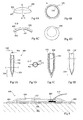
- Figure 4A illustrates an ophthalmic element 400 comprising graphene that is adapted to be placed on the surface of the eye.
- the element 400 is for example in the form of a curved plate, the outer edge of which is circular in the example of Figures 4A to 4D , but could have a different shape.
- the element 400 for example has a concave underside 402 for contacting the surface of the eye, and a convex outer surface 404, having a form that permits an eyelid to close over the element 400.
- the element 400 for example has a diameter of between 8 and 20 mm.
- Figure 4B is an underside view of the element 400 in a direction represented by an arrow A in Figure 4 looking towards the concave side of the element.
- the element for example comprises a graphene film 100 and a polymer support layer 102.
- the graphene film 100 is for example exposed on the inside surface of the element 400, such that it can make electrical contact with the surface of an eye.
- the polymer layer 102 provides a support for the graphene film 100, and is formed in contact with the graphene film 100 and exposed on the outer surface of the element 400.
- the polymer material used for the support 102 is for example parylene, in view of the biocompatible nature of this polymer.
- Figure 4C illustrates a cross-section B-B through the element of Figure 4A , and as illustrated, the graphene film 100 and polymer support 102 together form a curved multi-layer.
- Figure 4D represents a method step during the fabrication of the ophthalmic element 400 according to an example embodiment.
- the element is for example formed using a substantially spherical substrate, for example formed of a ball of copper, having at least approximately the dimensions of a human eye.
- the graphene film 100 is then for example formed by CVD on this substrate, and a polymer layer 102 is deposited by gas phase deposition over the graphene film 100.
- a portion of the graphene/polymer multi-layer is then for example cut from the sphere in the shape of the ophthalmic element 400 and separated from the substrate, for example by a delamination process as described above, or by etching the copper forming the substrate.
- an electrochemical delamination process may be performed as described in more detail in the publication entitled “ Electrochemical delamination of CVD-Grown Graphene Film: Toward the Recyclable Use of Copper Catalyst", Yu Wang et al., the contents of which is hereby incorporated by reference to the extent permitted by the law.
- the graphene film 100 could be patterned.
- the mold used to form the ophthalmic element could comprise two different materials, one of the materials supporting graphene growth and the other material not supporting graphene growth. The patterning of these two materials across the surface of the mold on which the graphene is to be formed is selected based on the desired graphene pattern.
- An example of a material not supporting graphene growth is aluminum oxide.
- a graphene etching step could be used to pattern the graphene film.
- the ophthalmic element 400 may have a variety of applications, including acting as an electrode on the surface of the eye.
- the ophthalmic element 400 could form the eye-mountable device described in the patent publication US2014/010744 , in which layers of ITO (indium tin oxide) are replaced by the graphene film described herein.
- other applications of the ophthalmic element 400 include an ophthalmic shielding device, for example for shielding the eye from electromagnetic radiation such as microwaves.
- Figure 5A is a cross-section view of a medical implant 500 comprising graphene.
- the element 500 is for example adapted to be inserted into human or animal tissue to act as an electrode.
- the implant is used to monitor or stimulate neural activity.
- the implant is for example similar to the one disclosed in the US patent publication US2013/0090542 , the contents of which is hereby incorporated by reference to the extent permitted by the law.
- this document described an electrically conductive core material with an electrically non-conductive biocompatible polymer coating
- the implant of Figure 5A comprises a polymer core having an electrically conductive coating formed by a graphene film.
- the implant 500 for example comprises a polymer core 502 in the form of a needle, for example of parylene or polyimide, covered by a graphene film 100.
- the element 500 has a pointed end 504, which in the example of Figure 5D has its point aligned with an axis 506 of the shaft of the needle, although in alternative embodiments the point coupled be offset with respect to this axis.
- the implant for example has a length of between a few millimeters and up to several tens of centimeters, depending on the application.
- some portions of the outer surface of the implant 500 could be formed of material other than graphene.
- the point of the implant 500 could be formed of silicon or another material.
- the implant comprises, for example at an opposite end to the point 504, an electrode 508, which contacts the graphene film 100.
- the electrode 508 for example electrically couples the graphene film 100 to a wire 510, allowing electrical signals to be applied to the implant and/or electrical signals from the implant to be detected.
- Figure 5B is a cross-section view taken along a line C-C of Figure 5A traversing a shaft of the implant between the pointed end 504 and the electrode 508.
- the implant is for example substantially circular in cross-section, although in alternative embodiment other shapes would be possible.
- a diameter of the implant is for example in the range 20 ⁇ m to 500 ⁇ m.
- Figures 5C and 5D are cross-section views illustrating examples of process steps for forming the implant 500 of Figure 5A .
- the implant of Figure 5A is for example formed using a mold 508, for example formed of copper, and having an inside surface having the desired outer form of the implant 500.
- the graphene film 100 is then for example formed by CVD on the inside surface of the mold, for example using the chamber 202 of the apparatus of Figure 2 .
- a gas phase deposition of the polymer support 502 is then performed to fill the mold 508, and contact the graphene film 100.
- the mold 508 is then removed, for example using an etching step, leaving the shaft and pointed end 504 of the implant 500.
- the electrode 508 (not shown in Figure 5D ) is for example in the form of a cap placed over the end of the implant, opposite to the pointed end 504.
- the electrode 508 could be formed by a portion of the mold that is for example protected so that it is not etched when the rest of the mold is removed, and which thus remains in contact with the graphene film 100.
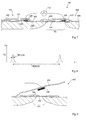
- Figure 6 is a cross-section view of a conductive patch 600 comprising a graphene film 100.
- Figure 6 illustrates an example in which the patch is employed contacting the surface of a portion of skin 602 of a human or animal body.
- the graphene film 100 of the patch is for example positioned to be exposed to and make contact directly with the surface of the skin 602, and it has a support 102 of polymer material in the form of a layer formed over it.
- the polymer layer 102 is for example of parylene.
- a further band 604 of polymer for example covers the graphene and polymer multi-layer 100, 102, and holds it in place against the skin. For this, the band 604 for example extends beyond the multi-layer 100, 102 on each side to make direct contact with the surface of the skin 602. It also for example has an adhesive layer 606 over at least a portion of its surface that contacts with the skin 602.
- An electrode 608 for example contacts the graphene film.
- the polymer layer 102 for example has a thickness of between 10 nm and 5 mm, and an opening is formed in a portion of the polymer layer 102 in order to expose the surface of the graphene film.
- the electrode 608 is then for example formed on the graphene film, and in some embodiments, a further polymer deposition is performed to cover the electrode 608.
- An antenna 610 for example couples the electrode 608 to a monitoring device, passing through the band 604.
- the patch 600 of Figure 6 is only represented in cross-section, and it will be clear to those skilled on the art that in plan view the graphene/polymer multi-layer 100, 102, and the band 604, could have any form, for example rectangular or circular.
- the graphene film 100 for example has a surface area of between 5 and 50 mm 2 that contacts the skin 602.
- graphene/polymer multi-layer 100, 102 is relatively supple, enabling it to follow contours in the surface of the skin, including wrinkles, while maintaining relatively high conductivity with the skin 602.
- the patch 600 could be used for administering a medicine and/or for the treatment of open wounds, as will now be described in more detail with reference to Figures 7 and 8 .
- FIG 7 illustrates an apparatus 700 for treating wounds and/or administering medicine using the medical patch 600 of Figure 6 .
- the patch 600 is for example applied covering an open wound 701.
- the patch 600 could be applied to skin in a similar fashion to the example of Figure 6 , and used for drug delivery.
- a further patch 702 which is for example very similar to the patch 600, is for example applied to the patient's skin in the vicinity of the wound, for example within a distance of 20 cm or so from the wound.
- the features of the patch 702 have been labelled with like reference numerals to the patch 600, and will not be described again in detail.
- a different type of conductive patch could be used to implement the further patch 702.
- the electrodes 608 of each of the patches 600, 702 are for example coupled to a voltage application module 710.
- the module 710 is for example adapted to apply voltage pulses across the electrodes 608 of the patches 600, 702 in order to drive a current through the patient's tissue in the vicinity of the wound 701 or the patient's skin.
- Medicine is for example delivered through the skin by the patch 600 using a process of iontophoresis.
- the medicine is for example in the form of a cream or gel positioned between the graphene film 100 and the skin.
- a DC current of between 0.1 and 5 mA is for example applied between the electrodes of the patches 600, 700.
- a voltage in the range 5 to 40 V is for example applied between the electrodes of the patches 600, 700.
- a pulsed signal rather than a DC signal could be applied.
- a process of electrical stimulation is for example performed, as described in more detail in the publication by L.C. Kloth entitled “Electrical Stimulation Technologies for Wound Healing", Adv Wound Care, Feb 1, 2014, 3(2): 81-90 , the contents of which is hereby incorporated by reference.
- a DC signal could be applied, for example having a voltage in the range of 5 to 60 V.
- a monophasic or diphasic pulsed current could be applied, having a frequency of anywhere between 1 and 100 kHz, and a voltage for example in the range 50 to 500 V.
- Figure 8 illustrates an example of the voltage signal applied to across the electrodes 608 of the patches 600, 702 to provide electrical stimulation for wound healing.
- the voltage pulses have a peak voltage amplitude Vp of around 100 V.
- Each pulse for example has a duration t PULSE , and the no-current interval between successive pulses represents up to 99% or more of each period T PERIOD , such that the total current per second delivered to tissue does not exceed more than 1.2-1.5 mA.
- the paired pulse charge is for example only around 3-3.5 ⁇ C, and for a pulse rate of 100 pulses/s, the total charge accumulation (dosage) does not for example exceed 350 ⁇ C/s.
- Such a treatment is for example applied for a period of between 5 and 60 minutes, and repeated on a daily basis until the wound has healed.
- At least part of the graphene film 100 of the patch 600 remains in place on the tissue of the patient when the patch is removed, as will now be described with reference to Figure 9 .
- Figure 9 illustrates the patch 600 in the process of being removed, for example after the wound 701 has started to heal and has thus reduced in size.
- the band 604 and the electrode 608 of the patch 600 for example separate from the multi-layer of graphene 100 and polymer 102, which remain covering the wound 701.
- an adhesive is present between the protrusion formed by the electrode 608 and the band 604, such that the electrode is pulled away as the band 604 is removed from the skin.
- graphene is a material that will be progressively absorbed by tissue.
- a polymer layer that is relatively thin for example formed of parylene of between 10 and 20 nm in thickness, can also be absorbed.
- the graphene layer 100 may be a multi-layer, and the polymer layer 102 may be glued or otherwise fixed to the band 604, such that the patch delaminates within the graphene layer 100.
- the polymer layer 102 may be glued or otherwise fixed to the band 604, such that the patch delaminates within the graphene layer 100.
- only one or a few graphene layers for example remain covering the wound when the patch 600 is removed.
- the advantage of leaving at least part of the graphene/polymer multi-layer covering the wound when the patch 600 is removed is that this reduces damage to wound caused by the removal process, and further reduces the chance of infection by leaving a barrier in place.
- An advantage of the medical devices described herein is that they have a good electrical conductively due to the graphene film, and are capable of maintaining close electrical contact with the skin or tissue of the human or animal due to the use of the polymer material supporting the graphene film which adapts to contours in the surface of the body against which the device is applied.
Landscapes
- Health & Medical Sciences (AREA)
- Veterinary Medicine (AREA)
- Public Health (AREA)
- General Health & Medical Sciences (AREA)
- Animal Behavior & Ethology (AREA)
- Life Sciences & Earth Sciences (AREA)
- Chemical & Material Sciences (AREA)
- Epidemiology (AREA)
- Engineering & Computer Science (AREA)
- Heart & Thoracic Surgery (AREA)
- Biomedical Technology (AREA)
- Medicinal Chemistry (AREA)
- Radiology & Medical Imaging (AREA)
- Nuclear Medicine, Radiotherapy & Molecular Imaging (AREA)
- Transplantation (AREA)
- Oral & Maxillofacial Surgery (AREA)
- Dermatology (AREA)
- Inorganic Chemistry (AREA)
- Vascular Medicine (AREA)
- Surgery (AREA)
- Organic Chemistry (AREA)
- Cardiology (AREA)
- Materials Engineering (AREA)
- Nanotechnology (AREA)
- Materials For Medical Uses (AREA)
- Carbon And Carbon Compounds (AREA)
- Chemical Kinetics & Catalysis (AREA)
- Polymers & Plastics (AREA)
Priority Applications (7)
| Application Number | Priority Date | Filing Date | Title |
|---|---|---|---|
| EP15305351.7A EP3067073A1 (fr) | 2015-03-09 | 2015-03-09 | Procédé de formation d'un dispositif médical contenant du graphène |
| US15/556,984 US11040191B2 (en) | 2015-03-09 | 2016-03-09 | Method of forming a medical device comprising graphene |
| EP16709027.3A EP3268057B1 (fr) | 2015-03-09 | 2016-03-09 | Procédé de formation d'un dispositif médical contenant du graphène |
| ES16709027T ES2837109T3 (es) | 2015-03-09 | 2016-03-09 | Método de formación de un dispositivo médico que comprende grafeno |
| PCT/EP2016/054964 WO2016142401A1 (fr) | 2015-03-09 | 2016-03-09 | Procédé de formation d'un dispositif médical comprenant du graphène |
| CN201680026580.9A CN107624074B (zh) | 2015-03-09 | 2016-03-09 | 用于形成包含石墨烯的医疗装置的方法 |
| US17/346,003 US12059560B2 (en) | 2015-03-09 | 2021-06-11 | Method of forming a device comprising graphene |
Applications Claiming Priority (1)
| Application Number | Priority Date | Filing Date | Title |
|---|---|---|---|
| EP15305351.7A EP3067073A1 (fr) | 2015-03-09 | 2015-03-09 | Procédé de formation d'un dispositif médical contenant du graphène |
Publications (1)
| Publication Number | Publication Date |
|---|---|
| EP3067073A1 true EP3067073A1 (fr) | 2016-09-14 |
Family
ID=52737029
Family Applications (2)
| Application Number | Title | Priority Date | Filing Date |
|---|---|---|---|
| EP15305351.7A Withdrawn EP3067073A1 (fr) | 2015-03-09 | 2015-03-09 | Procédé de formation d'un dispositif médical contenant du graphène |
| EP16709027.3A Active EP3268057B1 (fr) | 2015-03-09 | 2016-03-09 | Procédé de formation d'un dispositif médical contenant du graphène |
Family Applications After (1)
| Application Number | Title | Priority Date | Filing Date |
|---|---|---|---|
| EP16709027.3A Active EP3268057B1 (fr) | 2015-03-09 | 2016-03-09 | Procédé de formation d'un dispositif médical contenant du graphène |
Country Status (5)
| Country | Link |
|---|---|
| US (1) | US11040191B2 (fr) |
| EP (2) | EP3067073A1 (fr) |
| CN (1) | CN107624074B (fr) |
| ES (1) | ES2837109T3 (fr) |
| WO (1) | WO2016142401A1 (fr) |
Cited By (3)
| Publication number | Priority date | Publication date | Assignee | Title |
|---|---|---|---|---|
| WO2021148716A1 (fr) * | 2020-01-21 | 2021-07-29 | Teknologian Tutkimuskeskus Vtt Oy | Électrode sèche pour une mesure biométrique sur une peau et son procédé de fabrication |
| WO2021226353A1 (fr) * | 2020-05-06 | 2021-11-11 | Novocure Gmbh | Tampon conducteur générant un champ de traitement de tumeur et méthodes de production et d'utilisation de celui-ci |
| GR1010778B (el) * | 2023-07-18 | 2024-10-01 | Ιδρυμα Τεχνολογιας Και Ερευνας/Ινστιτουτο Επιστημων Χημικης Μηχανικης, | Λεπτα και ευκαμπτα νανοσυνθετα θερμαντικα στοιχεια με βαση το γραφενιο χημικης εναποθεσης |
Families Citing this family (13)
| Publication number | Priority date | Publication date | Assignee | Title |
|---|---|---|---|---|
| US12059560B2 (en) | 2015-03-09 | 2024-08-13 | Centre National De La Recherche Scientifique | Method of forming a device comprising graphene |
| FR3033554B1 (fr) | 2015-03-09 | 2020-01-31 | Centre National De La Recherche Scientifique | Procede de formation d'un dispositif en graphene |
| FI127535B (en) * | 2016-03-15 | 2018-08-31 | Aalto Univ Foundation | Composite film comprising an electrically conductive layer |
| DE102017100192A1 (de) * | 2017-01-06 | 2018-07-12 | Cinogy Gmbh | Permanente Wundauflage mit Plasmaelektrode |
| CN107440835A (zh) * | 2017-09-07 | 2017-12-08 | 河南汇博医疗股份有限公司 | 一种微电流护创敷料 |
| CN108568029A (zh) * | 2018-03-14 | 2018-09-25 | 广州爱康医疗仪器有限公司 | 一种基于石墨烯的温热理疗电极片 |
| CN109806010B (zh) * | 2019-01-29 | 2022-01-28 | 苏州中科先进技术研究院有限公司 | 治疗头 |
| CN109768371B (zh) * | 2019-03-12 | 2024-07-09 | 吉林医药学院 | 用于康复护理装置的基于石墨烯的双频植入式天线 |
| CN110448798B (zh) * | 2019-07-17 | 2024-05-17 | 浙江诺尔康神经电子科技股份有限公司 | 石墨烯人工耳蜗电极及其制作方法 |
| WO2022258739A1 (fr) * | 2021-06-09 | 2022-12-15 | Inbrain Neuroelectronics Sl | Électrode médicale et agencement associé |
| CN114306753B (zh) * | 2021-12-15 | 2023-02-24 | 海宁市产业技术研究院 | 一种可植入式电刺激的导电支架及其制备方法 |
| CN114522001B (zh) * | 2022-02-22 | 2024-11-22 | 上海派拉纶生物技术股份有限公司 | 一种心轴润滑涂层 |
| EP4465032A1 (fr) | 2023-05-15 | 2024-11-20 | Grapheal | Dispositif de capteur électronique stratifié et procédé de fabrication |
Citations (9)
| Publication number | Priority date | Publication date | Assignee | Title |
|---|---|---|---|---|
| US20130090542A1 (en) | 2010-06-18 | 2013-04-11 | The Regents Of The University Of Michigan | Implantable micro-component electrodes |
| WO2013116675A1 (fr) * | 2012-02-01 | 2013-08-08 | Wayne State University | Électromouillage de diélectrique à l'aide de graphène |
| US20140010744A1 (en) | 2012-07-05 | 2014-01-09 | Ford Global Technologies, Llc | System and method for improving operation of an scr |
| US20140145139A1 (en) * | 2011-07-13 | 2014-05-29 | Ru Huang | Transparent flexible resistive memory and fabrication method thereof |
| EP2747158A1 (fr) * | 2012-12-24 | 2014-06-25 | Université Pierre et Marie Curie (Paris 6) | Electrode à base de carbone biocompatible, son utilisation et procédé de préparation |
| EP2778757A1 (fr) * | 2013-03-15 | 2014-09-17 | Johnson & Johnson Vision Care, Inc. | Dispositifs ophtalmiques avec transistors à semi-conducteur organique |
| US20140326700A1 (en) | 2013-05-06 | 2014-11-06 | Centre National De La Recherche Scientfique | Process and device for forming a graphene layer |
| CN102920452B (zh) * | 2012-11-02 | 2015-02-11 | 上海交通大学 | 基于石墨烯的柔性冠状心电电极及其制备方法 |
| WO2015020610A1 (fr) * | 2013-08-05 | 2015-02-12 | National University Of Singapore | Procédé de transfert face à face d'une couche bidimensionnelle développée sur une tranche revêtue d'une couche métallique, sur la tranche elle-même |
Family Cites Families (19)
| Publication number | Priority date | Publication date | Assignee | Title |
|---|---|---|---|---|
| GB0228375D0 (en) | 2002-12-05 | 2003-01-08 | Innovation And Entpr Off Of | Wound mapping |
| CN101048055A (zh) | 2006-03-30 | 2007-10-03 | 通用电气公司 | 先进的受热器和散热器 |
| JP5569769B2 (ja) * | 2009-08-31 | 2014-08-13 | 独立行政法人物質・材料研究機構 | グラフェンフィルム製造方法 |
| KR101405463B1 (ko) * | 2010-01-15 | 2014-06-27 | 그래핀스퀘어 주식회사 | 기체 및 수분 차단용 그래핀 보호막, 이의 형성 방법 및 그의 용도 |
| US8795257B2 (en) | 2010-07-19 | 2014-08-05 | Kci Licensing, Inc. | Systems and methods for electrically detecting the presence of exudate in dressings |
| EP3686719B1 (fr) | 2010-12-24 | 2024-08-14 | Graphene Square Inc. | Capteur tactile utilisant de la graphène pour détécter simultanément une pression et une position |
| CN102925859A (zh) | 2011-10-23 | 2013-02-13 | 常州碳元科技发展有限公司 | 一种具有保护层结构的碳层材料的制备方法 |
| US9177688B2 (en) | 2011-11-22 | 2015-11-03 | International Business Machines Corporation | Carbon nanotube-graphene hybrid transparent conductor and field effect transistor |
| KR101450963B1 (ko) * | 2012-07-27 | 2014-10-16 | 율촌화학 주식회사 | 적층 배리어 필름 |
| CN102988132A (zh) * | 2012-12-17 | 2013-03-27 | 中国科学院半导体研究所 | 用于视网膜修复或功能的全透明柔性电极 |
| CN105163682B (zh) | 2013-03-15 | 2018-06-01 | 圣犹达医疗用品电生理部门有限公司 | 力传感消融导管 |
| US20160030640A1 (en) * | 2013-03-15 | 2016-02-04 | New York Society For The Ruptured And Crippled Maintaining The Hospital For Special Surgery | Carbon nanotubes and graphene patches and implants for biological tissue |
| KR101513136B1 (ko) * | 2013-10-07 | 2015-04-17 | 한국과학기술연구원 | 그래핀 필름의 제조방법, 그래핀 필름, 및 이를 포함하는 전자 소자 |
| TWM487718U (zh) | 2014-01-15 | 2014-10-11 | Catz Inc | 導電貼片結構 |
| CN104000624B (zh) | 2014-04-24 | 2016-04-13 | 温州医科大学 | 一种贴于眼表用于眼轴测量的超声探头 |
| CN104257367B (zh) * | 2014-09-16 | 2016-04-06 | 苏州能斯达电子科技有限公司 | 一种可贴附柔性压力传感器及其制备方法 |
| US10073522B2 (en) | 2014-12-12 | 2018-09-11 | Regents Of The University Of Minnesota | Articles of handwear for sensing forces applied to medical devices |
| FR3033554B1 (fr) | 2015-03-09 | 2020-01-31 | Centre National De La Recherche Scientifique | Procede de formation d'un dispositif en graphene |
| US20170057827A1 (en) * | 2015-09-02 | 2017-03-02 | U.S.A. As Represented By The Administrator Of The National Aeronautics And Space Administration | Graphene transparent conductive electrode |
-
2015
- 2015-03-09 EP EP15305351.7A patent/EP3067073A1/fr not_active Withdrawn
-
2016
- 2016-03-09 ES ES16709027T patent/ES2837109T3/es active Active
- 2016-03-09 CN CN201680026580.9A patent/CN107624074B/zh active Active
- 2016-03-09 US US15/556,984 patent/US11040191B2/en active Active
- 2016-03-09 WO PCT/EP2016/054964 patent/WO2016142401A1/fr not_active Ceased
- 2016-03-09 EP EP16709027.3A patent/EP3268057B1/fr active Active
Patent Citations (9)
| Publication number | Priority date | Publication date | Assignee | Title |
|---|---|---|---|---|
| US20130090542A1 (en) | 2010-06-18 | 2013-04-11 | The Regents Of The University Of Michigan | Implantable micro-component electrodes |
| US20140145139A1 (en) * | 2011-07-13 | 2014-05-29 | Ru Huang | Transparent flexible resistive memory and fabrication method thereof |
| WO2013116675A1 (fr) * | 2012-02-01 | 2013-08-08 | Wayne State University | Électromouillage de diélectrique à l'aide de graphène |
| US20140010744A1 (en) | 2012-07-05 | 2014-01-09 | Ford Global Technologies, Llc | System and method for improving operation of an scr |
| CN102920452B (zh) * | 2012-11-02 | 2015-02-11 | 上海交通大学 | 基于石墨烯的柔性冠状心电电极及其制备方法 |
| EP2747158A1 (fr) * | 2012-12-24 | 2014-06-25 | Université Pierre et Marie Curie (Paris 6) | Electrode à base de carbone biocompatible, son utilisation et procédé de préparation |
| EP2778757A1 (fr) * | 2013-03-15 | 2014-09-17 | Johnson & Johnson Vision Care, Inc. | Dispositifs ophtalmiques avec transistors à semi-conducteur organique |
| US20140326700A1 (en) | 2013-05-06 | 2014-11-06 | Centre National De La Recherche Scientfique | Process and device for forming a graphene layer |
| WO2015020610A1 (fr) * | 2013-08-05 | 2015-02-12 | National University Of Singapore | Procédé de transfert face à face d'une couche bidimensionnelle développée sur une tranche revêtue d'une couche métallique, sur la tranche elle-même |
Non-Patent Citations (7)
| Title |
|---|
| I. KHRAPACH ET AL.: "Novel Highly Conductive and Transparent Graphene-Based Conductors", ADVANCED MATERIALS, vol. 24, 2012, pages 2844 - 2849, XP002728448, DOI: doi:10.1002/ADMA.201200489 |
| L. C. KLOTH: "Electrical Stimulation for Wound Healing: A Review of Evidence From In Vitro Studies, Animal Experiments, and Clinical Trials", THE INTERNATIONAL JOURNAL OF LOWER EXTREMITY WOUNDS, vol. 4, no. 1, 1 March 2005 (2005-03-01), pages 23 - 44, XP055212717, ISSN: 1534-7346, DOI: 10.1177/1534734605275733 * |
| L.C. KLOTH: "Electrical Stimulation Technologies for Wound Healing", ADV WOUND CARE, vol. 3, no. 2, 1 February 2014 (2014-02-01), pages 81 - 90 |
| PATRICIA DURÁN OSPINA ET AL: "A Review in Innovation in Ocular Prostheses and Visual Implants: New Biomaterials and Neuro-Implants is the Challenge for the Visual Care", JOURNAL OF OCULAR DISEASES AND THERAPEUTICS, vol. 2, 3 July 2014 (2014-07-03), pages 9 - 16, XP055212711 * |
| WANG Y ET AL: "Electrochemical delamination of CVD-grown graphene film: Toward the recyclable use of copper catalyst", ACS NANO, AMERICAN CHEMICAL SOCIETY, US, vol. 5, no. 12, 27 December 2011 (2011-12-27), pages 9927 - 9933, XP002716759, ISSN: 1936-0851, [retrieved on 20111104], DOI: 10.1021/NN203700W * |
| YU WANG, ELECTROCHEMICAL DELAMINATION OF CVD-GROWN GRAPHENE FILM: TOWARD THE RECYCLABLE USE OF COPPER CATALYST |
| Z. HAN ET AL.: "Homogeneous Optical and Electronic Properties of Graphene Due to the Suppression of Multilayer Patches During CVD on Copper Foils", ADV. FUNCT. MATER., 2013 |
Cited By (10)
| Publication number | Priority date | Publication date | Assignee | Title |
|---|---|---|---|---|
| WO2021148716A1 (fr) * | 2020-01-21 | 2021-07-29 | Teknologian Tutkimuskeskus Vtt Oy | Électrode sèche pour une mesure biométrique sur une peau et son procédé de fabrication |
| WO2021226353A1 (fr) * | 2020-05-06 | 2021-11-11 | Novocure Gmbh | Tampon conducteur générant un champ de traitement de tumeur et méthodes de production et d'utilisation de celui-ci |
| US12420089B2 (en) | 2020-05-06 | 2025-09-23 | Novocure Gmbh | Conductive pad with improved air flow and methods of production and use thereof |
| US12427308B2 (en) | 2020-05-06 | 2025-09-30 | Novocure Gmbh | Pad with improved air flow and methods of production and use thereof |
| US12434052B2 (en) | 2020-05-06 | 2025-10-07 | Novocure Gmbh | Breathable pad generating tumor treating field and methods of production and use thereof |
| US12440671B2 (en) | 2020-05-06 | 2025-10-14 | Novocure Gmbh | Conductive pad with improved air flow and methods of production and use thereof |
| US12465760B2 (en) | 2020-05-06 | 2025-11-11 | Novocure Gmbh | Pad generating tumor treating field and having kirigami-like cuts |
| US12472353B2 (en) | 2020-05-06 | 2025-11-18 | Novocure Gmbh | Transducer array flexibility and methods of production and use thereof |
| US12569677B2 (en) | 2020-05-06 | 2026-03-10 | Novocure Gmbh | Conductive pad incorporating a conductive fabric material |
| GR1010778B (el) * | 2023-07-18 | 2024-10-01 | Ιδρυμα Τεχνολογιας Και Ερευνας/Ινστιτουτο Επιστημων Χημικης Μηχανικης, | Λεπτα και ευκαμπτα νανοσυνθετα θερμαντικα στοιχεια με βαση το γραφενιο χημικης εναποθεσης |
Also Published As
| Publication number | Publication date |
|---|---|
| US11040191B2 (en) | 2021-06-22 |
| CN107624074B (zh) | 2021-05-18 |
| ES2837109T3 (es) | 2021-06-29 |
| WO2016142401A1 (fr) | 2016-09-15 |
| CN107624074A (zh) | 2018-01-23 |
| EP3268057A1 (fr) | 2018-01-17 |
| US20180056057A1 (en) | 2018-03-01 |
| EP3268057B1 (fr) | 2020-09-16 |
Similar Documents
| Publication | Publication Date | Title |
|---|---|---|
| EP3268057B1 (fr) | Procédé de formation d'un dispositif médical contenant du graphène | |
| US9174043B2 (en) | Methods for surgical wound dressing incorporating connected hydrogel beads having an embedded electrode therein | |
| EP1404406B1 (fr) | Carte electronique pour administration transdermique de medicaments et extraction d'analyte | |
| EP1235615B1 (fr) | Electrodes biomedicales et electrodes biomedicales pour electrostimulation | |
| CN102764154B (zh) | 用于将电流施加到皮肤的电手术装置 | |
| US12059560B2 (en) | Method of forming a device comprising graphene | |
| CN109998533A (zh) | 一种柔性微针电极阵列装置及制备方法 | |
| WO2016186501A2 (fr) | Dispositif plasma non thermique | |
| EP1750798A1 (fr) | Electrodes de fourniture continue d'energie | |
| JP2010536406A5 (fr) | ||
| WO2019046333A1 (fr) | Système de traitement par micro-aiguilles | |
| EP4462234A2 (fr) | Procédé de formation d'un dispositif au graphène | |
| US12097367B2 (en) | Wireless iontophoresis patch and controller | |
| EP3890636A1 (fr) | Structure de microlame et procédé de traitement de tissu | |
| KR20210146099A (ko) | 피부 치료용 마이크로 니들 장치 및 그 제조 방법 | |
| CN104093447A (zh) | 用于处理伤口的装置 | |
| EP3329961A1 (fr) | Dérivation implantable pour stimuler des nerfs complexes et son procédé de fabrication | |
| WO2023172680A1 (fr) | Dispositif de stimulation nerveuse pour la gestion de la douleur chronique | |
| WO2025111744A1 (fr) | Électrode à ballonnet à canaux multiples, son procédé de préparation et son utilisation |
Legal Events
| Date | Code | Title | Description |
|---|---|---|---|
| PUAI | Public reference made under article 153(3) epc to a published international application that has entered the european phase |
Free format text: ORIGINAL CODE: 0009012 |
|
| AK | Designated contracting states |
Kind code of ref document: A1 Designated state(s): AL AT BE BG CH CY CZ DE DK EE ES FI FR GB GR HR HU IE IS IT LI LT LU LV MC MK MT NL NO PL PT RO RS SE SI SK SM TR |
|
| AX | Request for extension of the european patent |
Extension state: BA ME |
|
| STAA | Information on the status of an ep patent application or granted ep patent |
Free format text: STATUS: THE APPLICATION IS DEEMED TO BE WITHDRAWN |
|
| 18D | Application deemed to be withdrawn |
Effective date: 20170315 |