EP3067360A1 - Composé organométallique et dispositif électroluminescent organique l'incluant - Google Patents
Composé organométallique et dispositif électroluminescent organique l'incluant Download PDFInfo
- Publication number
- EP3067360A1 EP3067360A1 EP16159719.0A EP16159719A EP3067360A1 EP 3067360 A1 EP3067360 A1 EP 3067360A1 EP 16159719 A EP16159719 A EP 16159719A EP 3067360 A1 EP3067360 A1 EP 3067360A1
- Authority
- EP
- European Patent Office
- Prior art keywords
- group
- substituted
- sec
- tert
- pentyl
- Prior art date
- Legal status (The legal status is an assumption and is not a legal conclusion. Google has not performed a legal analysis and makes no representation as to the accuracy of the status listed.)
- Granted
Links
- 0 Cc1cccc(C)c1* Chemical compound Cc1cccc(C)c1* 0.000 description 6
- WRFHKSISCCSZEG-UHFFFAOYSA-N CC1(C)c(cc(cc2)N(C3(C)C=CC(c(cc4)cc(c5c6cccc5)c4[n]6-c4ccccc4)=CC3)c(cc3)ccc3-c3ccccc3)c2-c2ccccc12 Chemical compound CC1(C)c(cc(cc2)N(C3(C)C=CC(c(cc4)cc(c5c6cccc5)c4[n]6-c4ccccc4)=CC3)c(cc3)ccc3-c3ccccc3)c2-c2ccccc12 WRFHKSISCCSZEG-UHFFFAOYSA-N 0.000 description 1
- QKJWAFPHEYXCJB-UHFFFAOYSA-N COc(c(I)c(c(O)c1O)O)c1O Chemical compound COc(c(I)c(c(O)c1O)O)c1O QKJWAFPHEYXCJB-UHFFFAOYSA-N 0.000 description 1
- BFIMMTCNYPIMRN-UHFFFAOYSA-N Cc1cc(C)c(C)c(C)c1 Chemical compound Cc1cc(C)c(C)c(C)c1 BFIMMTCNYPIMRN-UHFFFAOYSA-N 0.000 description 1
Images
Classifications
-
- H—ELECTRICITY
- H10—SEMICONDUCTOR DEVICES; ELECTRIC SOLID-STATE DEVICES NOT OTHERWISE PROVIDED FOR
- H10K—ORGANIC ELECTRIC SOLID-STATE DEVICES
- H10K85/00—Organic materials used in the body or electrodes of devices covered by this subclass
- H10K85/40—Organosilicon compounds, e.g. TIPS pentacene
-
- C—CHEMISTRY; METALLURGY
- C07—ORGANIC CHEMISTRY
- C07F—ACYCLIC, CARBOCYCLIC OR HETEROCYCLIC COMPOUNDS CONTAINING ELEMENTS OTHER THAN CARBON, HYDROGEN, HALOGEN, OXYGEN, NITROGEN, SULFUR, SELENIUM OR TELLURIUM
- C07F15/00—Compounds containing elements of Groups 8, 9, 10 or 18 of the Periodic Table
- C07F15/0006—Compounds containing elements of Groups 8, 9, 10 or 18 of the Periodic Table compounds of the platinum group
- C07F15/0033—Iridium compounds
-
- C—CHEMISTRY; METALLURGY
- C09—DYES; PAINTS; POLISHES; NATURAL RESINS; ADHESIVES; COMPOSITIONS NOT OTHERWISE PROVIDED FOR; APPLICATIONS OF MATERIALS NOT OTHERWISE PROVIDED FOR
- C09K—MATERIALS FOR MISCELLANEOUS APPLICATIONS, NOT PROVIDED FOR ELSEWHERE
- C09K11/00—Luminescent materials, e.g. electroluminescent or chemiluminescent
- C09K11/06—Luminescent materials, e.g. electroluminescent or chemiluminescent containing organic luminescent materials
-
- H—ELECTRICITY
- H10—SEMICONDUCTOR DEVICES; ELECTRIC SOLID-STATE DEVICES NOT OTHERWISE PROVIDED FOR
- H10K—ORGANIC ELECTRIC SOLID-STATE DEVICES
- H10K50/00—Organic light-emitting devices
-
- H—ELECTRICITY
- H10—SEMICONDUCTOR DEVICES; ELECTRIC SOLID-STATE DEVICES NOT OTHERWISE PROVIDED FOR
- H10K—ORGANIC ELECTRIC SOLID-STATE DEVICES
- H10K50/00—Organic light-emitting devices
- H10K50/10—OLEDs or polymer light-emitting diodes [PLED]
- H10K50/11—OLEDs or polymer light-emitting diodes [PLED] characterised by the electroluminescent [EL] layers
-
- H—ELECTRICITY
- H10—SEMICONDUCTOR DEVICES; ELECTRIC SOLID-STATE DEVICES NOT OTHERWISE PROVIDED FOR
- H10K—ORGANIC ELECTRIC SOLID-STATE DEVICES
- H10K85/00—Organic materials used in the body or electrodes of devices covered by this subclass
- H10K85/30—Coordination compounds
- H10K85/341—Transition metal complexes, e.g. Ru(II)polypyridine complexes
- H10K85/342—Transition metal complexes, e.g. Ru(II)polypyridine complexes comprising iridium
-
- H—ELECTRICITY
- H10—SEMICONDUCTOR DEVICES; ELECTRIC SOLID-STATE DEVICES NOT OTHERWISE PROVIDED FOR
- H10K—ORGANIC ELECTRIC SOLID-STATE DEVICES
- H10K85/00—Organic materials used in the body or electrodes of devices covered by this subclass
- H10K85/60—Organic compounds having low molecular weight
- H10K85/615—Polycyclic condensed aromatic hydrocarbons, e.g. anthracene
- H10K85/626—Polycyclic condensed aromatic hydrocarbons, e.g. anthracene containing more than one polycyclic condensed aromatic rings, e.g. bis-anthracene
-
- H—ELECTRICITY
- H10—SEMICONDUCTOR DEVICES; ELECTRIC SOLID-STATE DEVICES NOT OTHERWISE PROVIDED FOR
- H10K—ORGANIC ELECTRIC SOLID-STATE DEVICES
- H10K85/00—Organic materials used in the body or electrodes of devices covered by this subclass
- H10K85/60—Organic compounds having low molecular weight
- H10K85/631—Amine compounds having at least two aryl rest on at least one amine-nitrogen atom, e.g. triphenylamine
- H10K85/633—Amine compounds having at least two aryl rest on at least one amine-nitrogen atom, e.g. triphenylamine comprising polycyclic condensed aromatic hydrocarbons as substituents on the nitrogen atom
-
- H—ELECTRICITY
- H10—SEMICONDUCTOR DEVICES; ELECTRIC SOLID-STATE DEVICES NOT OTHERWISE PROVIDED FOR
- H10K—ORGANIC ELECTRIC SOLID-STATE DEVICES
- H10K85/00—Organic materials used in the body or electrodes of devices covered by this subclass
- H10K85/60—Organic compounds having low molecular weight
- H10K85/631—Amine compounds having at least two aryl rest on at least one amine-nitrogen atom, e.g. triphenylamine
- H10K85/636—Amine compounds having at least two aryl rest on at least one amine-nitrogen atom, e.g. triphenylamine comprising heteroaromatic hydrocarbons as substituents on the nitrogen atom
-
- H—ELECTRICITY
- H10—SEMICONDUCTOR DEVICES; ELECTRIC SOLID-STATE DEVICES NOT OTHERWISE PROVIDED FOR
- H10K—ORGANIC ELECTRIC SOLID-STATE DEVICES
- H10K85/00—Organic materials used in the body or electrodes of devices covered by this subclass
- H10K85/60—Organic compounds having low molecular weight
- H10K85/649—Aromatic compounds comprising a hetero atom
- H10K85/657—Polycyclic condensed heteroaromatic hydrocarbons
- H10K85/6572—Polycyclic condensed heteroaromatic hydrocarbons comprising only nitrogen in the heteroaromatic polycondensed ring system, e.g. phenanthroline or carbazole
-
- C—CHEMISTRY; METALLURGY
- C09—DYES; PAINTS; POLISHES; NATURAL RESINS; ADHESIVES; COMPOSITIONS NOT OTHERWISE PROVIDED FOR; APPLICATIONS OF MATERIALS NOT OTHERWISE PROVIDED FOR
- C09K—MATERIALS FOR MISCELLANEOUS APPLICATIONS, NOT PROVIDED FOR ELSEWHERE
- C09K2211/00—Chemical nature of organic luminescent or tenebrescent compounds
- C09K2211/10—Non-macromolecular compounds
- C09K2211/1003—Carbocyclic compounds
- C09K2211/1007—Non-condensed systems
-
- C—CHEMISTRY; METALLURGY
- C09—DYES; PAINTS; POLISHES; NATURAL RESINS; ADHESIVES; COMPOSITIONS NOT OTHERWISE PROVIDED FOR; APPLICATIONS OF MATERIALS NOT OTHERWISE PROVIDED FOR
- C09K—MATERIALS FOR MISCELLANEOUS APPLICATIONS, NOT PROVIDED FOR ELSEWHERE
- C09K2211/00—Chemical nature of organic luminescent or tenebrescent compounds
- C09K2211/10—Non-macromolecular compounds
- C09K2211/1018—Heterocyclic compounds
- C09K2211/1025—Heterocyclic compounds characterised by ligands
- C09K2211/1029—Heterocyclic compounds characterised by ligands containing one nitrogen atom as the heteroatom
-
- C—CHEMISTRY; METALLURGY
- C09—DYES; PAINTS; POLISHES; NATURAL RESINS; ADHESIVES; COMPOSITIONS NOT OTHERWISE PROVIDED FOR; APPLICATIONS OF MATERIALS NOT OTHERWISE PROVIDED FOR
- C09K—MATERIALS FOR MISCELLANEOUS APPLICATIONS, NOT PROVIDED FOR ELSEWHERE
- C09K2211/00—Chemical nature of organic luminescent or tenebrescent compounds
- C09K2211/18—Metal complexes
- C09K2211/185—Metal complexes of the platinum group, i.e. Os, Ir, Pt, Ru, Rh or Pd
-
- C—CHEMISTRY; METALLURGY
- C09—DYES; PAINTS; POLISHES; NATURAL RESINS; ADHESIVES; COMPOSITIONS NOT OTHERWISE PROVIDED FOR; APPLICATIONS OF MATERIALS NOT OTHERWISE PROVIDED FOR
- C09K—MATERIALS FOR MISCELLANEOUS APPLICATIONS, NOT PROVIDED FOR ELSEWHERE
- C09K2211/00—Chemical nature of organic luminescent or tenebrescent compounds
- C09K2211/18—Metal complexes
- C09K2211/188—Metal complexes of other metals not provided for in one of the previous groups
-
- H—ELECTRICITY
- H10—SEMICONDUCTOR DEVICES; ELECTRIC SOLID-STATE DEVICES NOT OTHERWISE PROVIDED FOR
- H10K—ORGANIC ELECTRIC SOLID-STATE DEVICES
- H10K2101/00—Properties of the organic materials covered by group H10K85/00
- H10K2101/10—Triplet emission
Definitions
- One or more embodiments relate to an organometallic compound and an organic light-emitting device including the same.
- Organic light emitting devices are self-emission devices that have wide viewing angles, high contrast ratios, short response times, and good brightness, driving voltage, and response speed characteristics, and produce full-color images.
- an organic light-emitting device includes an anode, a cathode, and an organic layer that is disposed between the anode and the cathode and includes an emission layer.
- a hole transport region may be disposed between the anode and the emission layer, and an electron transport region may be disposed between the emission layer and the cathode.
- Holes provided from the anode may move toward the emission layer through the hole transport region, and electrons provided from the cathode may move toward the emission layer through the electron transport region.
- the holes and the electrons are recombined in the emission layer to produce excitons. These excitons change from an excited state to a ground state, thereby generating light.
- One or more embodiments relate to a novel organometallic compound and an organic light-emitting device including the same.
- an organometallic compound represented by Formula 1 is provided: wherein in Formula 1,
- the organometallic compound may be included in the emission layer.
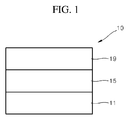
- FIG. 1 is a schematic view of an organic light-emitting device according to an embodiment.
- An organometallic compound according to an exemplary embodiment is represented by Formula 1:
- R 1 to R 3 in Formula 1 may be each independently selected from a hydrogen, a deuterium, -CH 3 , -CD 3 , -CD 2 H, -CDH 2 , -CH 2 CH 3 , -CH 2 CD 3 ,-CH 2 CD 2 H, -CH 2 CDH 2 , -CHDCH 3 , -CHDCD 2 H, -CHDCDH 2 , -CHDCD 3 , -CD 2 CD 3 ,-CD 2 CD 2 H, and -CD 2 CDH 2 ; an n-propyl group, an isopropyl group, an n-butyl group, an isobutyl group, a sec-butyl group, a tert-butyl group, an n-pentyl group, an isopentyl group, a sec-pentyl group, a tert-pentyl group, a phenyl group, a naphthyl group, and
- R 1 to R 3 in Formula 1 may be each independently selected from a hydrogen, a deuterium, -CH 3 , -CH 2 CH 3 , -CD 3 , -CD 2 H, -CDH 2 , -CH 2 CD 3 , and-CD 2 CH 3 .
- R 1 to R 3 in Formula 1 may be each independently selected from -CH 3 , -CH 2 CH 3 , -CD 3 , -CD 2 H, -CDH 2 , -CH 2 CD 3 , and -CD 2 CH 3 .
- R 1 to R 3 in Formula 1 may be each independently selected from a hydrogen, a deuterium, -CH 3 , -CD 3 , -CD 2 H, -CDH 2 , -CF 3 , -CF 2 H, -CFH 2 , groups represented by Formulae 9-1 to 9-19, and groups represented by Formulae 10-1 to 10-18: * in Formulae 9-1 to 9-19 and 10-1 to 10-18 is a binding site to a neighboring atom.
- R 1 to R 3 in Formula 1 may be each independently selected from -CH 3 , -CD 3 , -CD 2 H, -CDH 2 , groups represented by Formulae 9-1 to 9-19, and a phenyl group, but it may be considered that they are not limited thereto.
- R 1 to R 3 in Formula 1 may all be identical to each other.
- R 1 to R 3 may all be identical to each other, and R 1 to R 3 may be selected from -CH 3 , -CD 3 , -CD 2 H, -CDH 2 , groups represented by Formulae 9-1 to 9-19, and a phenyl group, but it may be considered that they are not limited thereto.
- R 11 to R 13 and R 21 in Formula 1 may be each independently selected from a hydrogen, a cyano group, a deuterium, -F, -Cl, -Br, -I, -SF 5 , a hydroxyl group, a nitro group, an amino group, an amidino group, a hydrazine group, a hydrazone group, a carboxylic acid group or a salt thereof, a sulfonic acid group or a salt thereof, a phosphoric acid group or a salt thereof, a substituted or unsubstituted C 1 -C 60 alkyl group, a substituted or unsubstituted C 2 -C 60 alkenyl group, a substituted or unsubstituted C 2 -C 60 alkynyl group, a substituted or unsubstituted C 1 -C 60 alkoxy group, a substituted or unsubstituted C 3 -C 10 cycloalkyl group
- R 11 to R 13 and R 21 in Formula 1 may be each independently selected from a hydrogen, a deuterium, -F, -Cl, -Br, -I, a hydroxyl group, a cyano group, a nitro group, an amino group, an amidino group, a hydrazine group, a hydrazone group, a carboxylic acid group or a salt thereof, a sulfonic acid group or a salt thereof, a phosphoric acid group or a salt thereof, -SF 5 , C 1 -C 20 alkyl group, and a C 1 -C 20 alkoxy group; a C 1 -C 20 alkyl group and a C 1 -C 20 alkoxy group, each substituted with at least one selected from a deuterium, -F, -Cl, -Br, -I, -CD 3 , -CD 2 H, -CDH 2 , -CF 3 , -
- R 11 to R 13 and R 21 in Formula 1 may be each independently selected from a hydrogen, a deuterium, -F, a cyano group, a nitro group, -SF 5 , a methyl group, an ethyl group, an n-propyl group, an isopropyl group, an n-butyl group, an isobutyl group, a sec-butyl group, a tert-butyl group, an n-pentyl group, an isopentyl group, a sec-pentyl group, a tert-pentyl group, an n-hexyl group, an iso-hexyl group, a sec-hexyl group, a tert-hexyl group, an n-heptyl group, an iso-heptyl group, a sec-heptyl group, a tert-heptyl group, an n-octy
- R 11 to R 13 and R 21 in Formula 1 may be each independently selected from a hydrogen, a deuterium, -F, a cyano group, a nitro group, -SF 5 , -CH 3 , -CD 3 , -CD 2 H, -CDH 2 , -CF 3 , -CF 2 H, -CFH 2 , groups represented by Formulae 9-1 to 9-19, and groups represented by Formulae 10-1 to 10-36, provided that at least one selected from to R 13 in Formula 1 is not a hydrogen: wherein * in Formulae 9-1 to 9-19 and 10-1 to 10-36 is a binding site to a neighboring atom.
- b1 in Formula 1 indicates the number of R 21 (s).
- b1 When CY 1 is a benzene ring, b1 may be an integer selected from 0 to 4. When CY 1 is a naphthalene ring, b1 may be an integer selected from 0 to 6.
- b1 When b1 is 2 or more, 2 or more R 21 (s) may be identical to or different from each other.
- b1 may be 0, 1, or 2.
- b1 may be 1.
- b1 in Formula 1 may be 0, but it may be considered that they are not limited thereto.
- R 11 in Formula 1 may not be a hydrogen.
- R 11 in Formula 1 may be neither a hydrogen nor a methyl group.
- R 11 may not be a hydrogen and R 12 and R 13 may each be a hydrogen; or R 12 may not be a hydrogen and R 11 and R 13 may be a hydrogen.
- R 12 in Formula 1 may be a deuterium, -F, -Cl, -Br, -I, -SF 5 , a hydroxyl group, a cyano group, a nitro group, an amino group, an amidino group, a hydrazine group, a hydrazone group, a carboxylic acid group or a salt thereof, a sulfonic acid group or a salt thereof, a phosphoric acid group or a salt thereof, a substituted or unsubstituted C 1 -C 20 alkyl group, a substituted or unsubstituted C 1 -C 20 alkoxy group, a substituted or unsubstituted C 3 -C 10 cycloalkyl group, a substituted or unsubstituted C 1 -C 10 heterocycloalkyl group, a substituted or unsubstituted C 3 -C 10 cycloalkenyl group, a substituted or unsubstit
- R 12 in Formula 1 may be selected from a deuterium, -F, -Cl, -Br, -I, a hydroxyl group, a cyano group, a nitro group, an amino group, an amidino group, a hydrazine group, a hydrazone group, a carboxylic acid group or a salt thereof, a sulfonic acid group or a salt thereof, a phosphoric acid group or a salt thereof, -SF 5 , C 1 -C 20 alkyl group, and a C 1 -C 20 alkoxy group; a C 1 -C 20 alkyl group and a C 1 -C 20 alkoxy group, each substituted with at least one selected from a deuterium, -F, -Cl, -Br, -I, -CD 3 , -CD 2 H, -CDH 2 , -CF 3 , -CF 2 H, -CFH 2 ,
- R 12 in Formula 1 may be a substituted or unsubstituted C 1 -C 20 alkyl group.
- R 12 in Formula 1 may be selected from a C 1 -C 20 alkyl group and a C 1 -C 20 alkoxy group; and a C 1 -C 20 alkyl group and a C 1 -C 20 alkoxy group, each substituted with at least one selected from a deuterium, -F, -Cl, -Br, -I, -CD 3 , -CD 2 H, -CDH 2 , -CF 3 , -CF 2 H, -CFH 2 , a hydroxyl group, a cyano group, a nitro group, an amino group, an amidino group, a hydrazine group, a hydrazone group, a carboxylic acid group or a salt thereof, a sulfonic group or a salt thereof, a phosphoric acid group or a salt thereof, a C 1 -C 10 alkyl group, a cyclopentyl group, a cyclohex
- R 12 in Formula 1 may be selected from a C 2 -C 20 alkyl group and a C 2 -C 20 alkoxy group; a methyl group and a methoxy group, each substituted with at least one selected from C 3 -C 10 cycloalkyl group, a C 1 -C 10 heterocycloalkyl group, a C 3 -C 10 cycloalkenyl group, a C 1 -C 10 heterocycloalkenyl group, a C 6 -C 14 aryl group, a C 1 -C 14 heteroaryl group, a monovalent non-aromatic condensed polycyclic group, and a monovalent non-aromatic condensed heteropolycyclic group; a C 2 -C 20 alkyl group and a C 2 -C 20 alkoxy group, each substituted with at least one selected from a deuterium, -F, -Cl, -Br, -I, -CD 3 ,
- R 12 in Formula 1 may be selected from a C 2 -C 20 alkyl group and a C 2 -C 20 alkoxy group; a methyl group and a methoxy group, each substituted with at least one selected a cyclopentyl group, a cyclohexyl group, a cycloheptyl group, a cyclooctyl group, an adamantanyl group, a norbornanyl group, a norbornenyl group, a cyclopentenyl group, a cyclohexenyl group, a cycloheptenyl group, a phenyl group, a naphthyl group, a pyridinyl group, and a pyrimidinyl group; a C 2 -C 20 alkyl group and a C 2 -C 20 alkoxy group, each substituted with at least one selected from a deuterium, -F, -Cl, -
- R 12 in Formula 1 may be selected from an ethyl group, an n-propyl group, an isopropyl group, an n-butyl group, an isobutyl group, a sec-butyl group, a tert-butyl group, an n-pentyl group, an isopentyl group, a sec-pentyl group, a tert-pentyl group, an n-hexyl group, an iso-hexyl group, a sec-hexyl group, a tert-hexyl group, an n-heptyl group, an iso-heptyl group, a sec-heptyl group, a tert-heptyl group, an n-octyl group, an iso-octyl group, a sec-octyl group, a tert-octyl group, an n-nonyl group
- R 12 in Formula 1 may be selected from a C 2 -C 20 alkyl group; a methyl group, each substituted with at least one selected from a C 3 -C 10 cycloalkyl group, a C 1 -C 10 heterocycloalkyl group, a C 3 -C 10 cycloalkenyl group, a C 1 -C 10 heterocycloalkenyl group, a C 6 -C 14 aryl group, a C 1 -C 14 heteroaryl group, a monovalent non-aromatic condensed polycyclic group, and a monovalent non-aromatic condensed heteropolycyclic group; and a C 2 -C 20 alkyl group, substituted with at least one selected from a deuterium, -F, - Cl, -Br, -I, -CD 3 , -CD 2 H, -CDH 2 , -CF 3 , -CF 2 H, -CFH 2 ,
- R 12 in Formula 1 may be selected from a C 2 -C 20 alkyl group; a methyl group, substituted with at least one selected from a cyclopentyl group, a cyclohexyl group, a cycloheptyl group, a cyclooctyl group, an adamantanyl group, a norbornanyl group, a norbornenyl group, a cyclopentenyl group, a cyclohexenyl group, a cycloheptenyl group, a phenyl group, a naphthyl group, a pyridinyl group, and a pyrimidinyl group; and a C 2 -C 20 alkyl group, substituted with at least one selected from a deuterium, -F, - Cl, -Br, -I, -CD 3 , -CD 2 H, -CDH 2 , -CF 3 , -
- R 12 in Formula 1 selected from an ethyl group, an n-propyl group, an isopropyl group, an n-butyl group, an isobutyl group, a sec-butyl group, a tert-butyl group, an n-pentyl group, an isopentyl group, a sec-pentyl group, a tert-pentyl group, an n-hexyl group, an iso-hexyl group, a sec-hexyl group, a tert-hexyl group, an n-heptyl group, an iso-heptyl group, a sec-heptyl group, a tert-heptyl group, an n-octyl group, an iso-octyl group, a sec-octyl group, a tert-octyl group, an n-nonyl group, an
- R 13 in Formula 1 may be selected from a deuterium, -F, -Cl, -Br, -I, a hydroxyl group, a cyano group, a nitro group, an amino group, an amidino group, a hydrazine group, a hydrazone group, a carboxylic acid group or a salt thereof, a sulfonic acid group or a salt thereof, a phosphoric acid group or a salt thereof, -SF 5 , a C 1 -C 20 alkyl group, and a C 1 -C 20 alkoxy group; a C 1 -C 20 alkyl group and a C 1 -C 20 alkoxy group, each substituted with at least one selected from a deuterium, -F, -Cl, -Br, -I, -CD 3 , -CD 2 H, -CDH 2 , -CF 3 , -CF 2 H, -CFH 2 , a
- the organometallic compound may be represented by one of Formulae 1-1 to 1-108:
- the organometallic compound may be represented by one of Formulae 1-1 to 1-48, 1-97 to 1-99 and 1-103 to 1-105 (provided that b1 in Formulae 1-97 to 1-99 and 1-103 to 1-105 is 0).
- the organometallic compound may be one of Compounds 1 to 96, but is not limited thereto:
- At least one selected from R 11 to R 13 in Formula 1 is not a hydrogen. That is, each of R 11 to R 13 in Formula 1 may not be a hydrogen at the same time. In some embodiments, R 12 in Formula 1 is not a hydrogen. In such conditions, the morphology of the organometallic compound represented by Formula 1 may be improved, and accordingly, a device, for example, an organic light-emitting device, including the organometallic compound may have a long lifespan.
- a silyl group (-Si(R 1 )(R 2 )(R 3 )) in Formula 1 (for example, Formulae 1-1 to 1-108) is bound to a fifth site of a pyridine ring, and each of R 11 to R 17 and R 21 is not a silyl group (see Formula 1 and Formulae 1-1 to 1-108, and definitions for R 11 to R 17 and R 21 ). That is, a silyl group in Formula 1 may be bound "only" to a fifth site of a pyridine ring.
- Formula 1 has identical three ligands. In such conditions, the organometallic compound represented by Formula 1 may have high triplet spin density and thermal stability at the same time. Accordingly, a device, for example, an organic light-emitting device, including the organometallic compound represented by Formula 1, may have high efficiency.
- organometallic compounds were evaluated by using a DFT method based on Gaussian program to measure their highest occupied molecular orbitals (HOMO), lowest unoccupied molecular orbitals (LUMO), and triplet (T 1 ) energy level (structally optimized at levels of B3LYP, 6-31G(d,p)). Evaluation results are shown in Table 1.
- Table 1 Compound No. HOMO(eV) LUMO(eV) T 1 energy level (eV) 1 -4.714 -1.184 2.567 2 -4.718 -1.158 2.572 13 -4.704 -1.120 2.612 32 -4.714 -1.184 2.567 Comparative material 1 -4.807 -1.205 2.604
- the rganometallic compound represented by Formula 1 has a HOMO level and a LUMO level, which are suitable for an organic light-emitting device, and is suitable for emitting light with luminescence energy (T 1 ) corresponding to visible light region.
- Synthesis methods of the organometallic compound represented by Formula 1 may be recognizable by one of ordinary skill in the art by referring to Synthesis Examples provided below.
- the organometallic compound represented by Formula 1 is suitable for use in an organic layer of an organic light-emitting device, for example, for use as a dopant in an emission layer of the organic layer.
- an organic light-emitting device that includes: a first electrode; a second electrode; and an organic layer that is disposed between the first electrode and the second electrode and includes an organic layer including an emission layer and at least one of the organometallic compounds represented by Formula 1.
- the organic light-emitting device may have, due to the inclusion of an organic layer including the organometallic compound represented by Formula 1, low driving voltage, high efficiency, high power, high quantum efficiency, long lifespan and excellent color.
- the organometallic compound of Formula 1 may be used between a pair of electrodes of an organic light-emitting device.
- the organometallic compound represented by Formula 1 may be included in the emission layer.
- the organometallic compound may act as a dopant, and the emission layer may further include host (that is, an amount of the organometallic compound represented by Formula 1 is smaller than an amount of the host).
- (an organic layer) includes at least one of the organometallic compounds used herein may include a case in which "(an organic layer) includes identical organometallic compounds of Formula 1 and a case in which (an organic layer) includes two or more different organometallic compounds of Formula 1.
- the organic layer may include, as the organometallic compound, only Compound 1.
- Compound 1 may exist in an emission layer of the organic light-emitting device.
- the organic layer may include, as the organometallic compound, Compound 1 and Compound 2.
- Compound 1 and Compound 2 may exist in an identical layer (for example, Compound 1 and Compound 2 all may exist in an emission layer).
- the first electrode may be an anode, which is a hole injection electrode, and the second electrode may be a cathode, which is an electron injection electrode; or the first electrode may be a cathode, which is an electron injection electrode, and the second electrode may be an anode, which is a hole injection electrode.
- the first electrode is an anode
- the second electrode is a cathode
- the organic layer includes i) a hole transport region that is between the first electrode and the emission layer and includes at least one selected from a hole injection layer, a hole transport layer, and an electron blocking layer, and ii) an electron transport region that is between the emission layer and the second electrode and includes at least one selected from a hole blocking layer, an electron transport layer, and an electron injection layer.
- organic layer refers to a single layer and/or a plurality of layers between the first electrode and the second electrode of an organic light-emitting device.
- the “organic layer” may include, in addition to an organic compound, an organometallic complex including metal.
- FIG. 1 is a schematic view of an organic light-emitting device 10 according to an embodiment.
- the organic light-emitting device 10 includes a first electrode 11, an organic layer 15, and a second electrode 19, which are sequentially stacked.
- a substrate may be additionally disposed under the first electrode 11 or above the second electrode 19.
- the substrate any substrate that is used in general organic light-emitting devices may be used, and the substrate may be a glass substrate or transparent plastic substrate, each with excellent mechanical strength, thermal stability, transparency, surface smoothness, ease of handling, and water-resistance first electrode 11 may be formed by depositing or sputtering a material for forming the first electrode on the substrate.
- the first electrode 11 may be an anode.
- the material for the first electrode 11 may be selected from materials with a high work function to allow holes be easily provided.
- the first electrode 11 may be a reflective electrode or a transmissive electrode.
- the material for the first electrode may be, for example, indium tin oxide (ITO), indium zinc oxide (IZO), tin oxide (SnO 2 ), and zinc oxide (ZnO).
- ITO indium tin oxide
- IZO indium zinc oxide
- SnO 2 tin oxide
- ZnO zinc oxide
- magnesium (Mg), aluminum (Al), aluminum-lithium (Al-Li), calcium (Ca), magnesium-indium (Mg-In), or magnesium-silver (Mg-Ag) may be used as the material for the first electrode.
- the first electrode 11 may have a single-layer structure or a multi-layer structure including two or more layers.
- the first electrode 11 may have a three-layered structure of ITO/Ag/ITO, but the structure of the first electrode 110 is not limited thereto.
- the organic layer 15 is disposed on the first electrode 11.
- the organic layer 15 may include a hole transport region, an emission layer, and an electron transport region.
- the hole transport region may be disposed between the first electrode 11 and the emission layer.
- the hole transport region may include at least one selected from a hole injection layer, a hole transport layer, an electron blocking layer, and a buffer layer.
- the hole transport region may include only either a hole injection layer or a hole transport layer.
- the hole transport region may have a structure of hole injection layer/hole transport layer or hole injection layer/hole transport layer/electron blocking layer, which are sequentially stacked in this stated order from the first electrode 11.
- a hole injection layer may be formed on the first electrode 11 by using various methods, such as vacuum deposition, spin coating, casting, or langmuir-blodgett (LB) deposition.
- the deposition conditions may vary according to a material that is used to form the hole injection layer, and the structure and thermal characteristics of the hole injection layer.
- the deposition conditions may include a deposition temperature of about 100 to about 500°C, a vacuum degree of about 10 -8 to about 10 -3 torr, and a deposition rate of about 0.001 to 10 nm/sec (0.01 to about 100 ⁇ /sec).
- the deposition conditions are not limited thereto.
- coating conditions may vary according to the material used to form the hole injection layer, and the structure and thermal properties of the hole injection layer.
- a coating speed may be from about 2000 rpm to about 5000 rpm
- a temperature at which a heat treatment is performed to remove a solvent after coating may be from about 80°C to about 200°C.
- the coating conditions are not limited thereto.
- Conditions for forming a hole transport layer and an electron blocking layer may be understood by referring to conditions for forming the hole injection layer.
- the hole transport region may include at least one selected from m-MTDATA, TDATA, 2-TNATA, NPB, ⁇ -NPB, TPD, Spiro-TPD, Spiro-NPB, methylated NPB, TAPC, HMTPD, 4,4',4"-tris(N-carbazolyl)triphenylamine (TCTA), polyaniline/dodecylbenzenesulfonic acid (Pani/DBSA), poly(3,4-ethylenedioxythiophene)/poly(4-styrenesulfonate) (PEDOT/PSS), polyaniline/camphor sulfonicacid (Pani/CSA), (polyaniline)/poly(4-styrenesulfonate) (Pani/PSS), a compound represented by Formula 201 below, and a compound represented by Formula 202 below:
- Ar 101 to Ar 102 in Formula 201 may be each independently selected from a phenylene group, a pentalenylene group, an indenylene group, a naphthylene group, an azulenylene group, a heptalenylene group, an acenaphthylene group, a fluorenylene group, a phenalenylene group, a phenanthrenylene group, an anthracenylene group, a fluoranthenylene group, a triphenylenylene group, a pyrenylene group, a chrysenylenylene group, a naphthacenylene group, a picenylene group, a perylenylene group, and a pentacenylene group; and a phenylene group, a pentalenylene group, an indenylene group, a naphthylene group, an azulenylene group, a heptalen
- xa and xb may be each independently an integer of 0 to 5, or 0, 1, or 2.
- R 101 to R 108 , R 111 to R 119 and R 121 to R 124 in Formulae 201 and 202 may be each independently selected from a hydrogen, a deuterium, -F, -Cl, -Br, -I, a hydroxyl group, a cyano group, a nitro group, an amino group, an amidino group, a hydrazine group, a hydrazone group, a carboxylic acid group or a salt thereof, a sulfonic acid group or a salt thereof, a phosphoric acid group or a salt thereof, a C 1 -C 10 alkyl group (for example, a methyl group, an ethyl group, a propyl group, a butyl group, a
- R 109 in Formula 201 may be selected from a phenyl group, a naphthyl group, an anthracenyl group, and a pyridinyl group; and a phenyl group, a naphthyl group, an anthracenyl group, and a pyridinyl group, each substituted with at least one selected from a deuterium, -F, -Cl, -Br, -I, a hydroxyl group, a cyano group, a nitro group, an amino group, an amidino group, a hydrazine group, a hydrazone group, a carboxylic acid group or a salt thereof, a sulfonic acid group or a salt thereof, a phosphoric acid group or a salt thereof, a C 1 -C 20 alkyl group, a C 1 -C 20 alkoxy group, a phenyl group, a naphthyl group, an anthrac
- the compound represented by Formula 201 may be represented by Formula 201A, but is not limited thereto:
- R 101 , R 111 , R 112 , and R 109 in Formula 201A may be understood by referring to the description provided herein.
- the compound represented by Formula 201 and the compound represented by Formula 202 may include compounds HT1 to HT20 illustrated below, but are not limited thereto.
- a thickness of the hole transport region may be in a range of about 10 nm (100 ⁇ ) about 1,000 nm (10000 ⁇ ) , for example, about 10 nm (100 ⁇ ) to about 100 nm (1000 ⁇ ).
- thickness of the hole injection layer may be in a range of about 10 nm (100 ⁇ ) to about nm (10000 ⁇ ) , and for example, about 10 nm (100 ⁇ ) to about 100 nm (1000 ⁇ )
- the thickness of the hole transport layer may be in a range of about 5 nm (50 ⁇ ) to about 200 (2000 ⁇ ), and for example, about 10 nm (100 ⁇ ) to about 150 nm (1500 ⁇ ).
- the hole transport region may further include, in addition to these materials, a charge-generation material for the improvement of conductive properties.
- the charge-generation material may be homogeneously or unhomogeneously dispersed in the hole transport region.
- the charge-generation material may be, for example, a p-dopant.
- the p-dopant may be one selected from a quinone derivative, a metal oxide, and a cyano group-containing compound, but embodiments are not limited thereto.
- Non-limiting examples of the p-dopant are a quinone derivative, such as tetracyanoquinonedimethane (TCNQ) or 2,3,5,6-tetrafluoro-tetracyano-1,4-benzoquinonedimethane (F4-TCNQ); a metal oxide, such as a tungsten oxide or a molybdenium oxide; and a cyano group-containing compound, such as Compound HT-D1 below, but are not limited thereto.
- a quinone derivative such as tetracyanoquinonedimethane (TCNQ) or 2,3,5,6-tetrafluoro-tetracyano-1,4-benzoquinonedimethane (F4-TCNQ)
- a metal oxide such as a tungsten oxide or a molybdenium oxide
- a cyano group-containing compound such as Compound HT-D1 below, but are not limited thereto.
- the hole transport region may include a buffer layer.
- the buffer layer may compensate for an optical resonance distance according to a wavelength of light emitted from the emission layer, and thus, efficiency of a formed organic light-emitting device may be improved.
- an emission layer may be formed on the hole transport region by vacuum deposition, spin coating, casting, LB deposition, or the like.
- the deposition or coating conditions may be similar to those applied to form the hole injection layer although the deposition or coating conditions may vary according to the material that is used to form the emission layer.
- a material for the electron blocking layer may be selected from materials for the hole transport region described above and materials for a host to be explained later.
- the material for the electron blocking layer is not limited thereto.
- a material for the electron blocking layer may be mCP, which will be explained later.
- the emission layer may include a host and a dopant, and the dopant may include the organometallic compound represented by Formula 1.
- the host may further include a compound represented by Formula 301 below.
- Ar 113 to Ar 116 in Formula 301 may be each independently selected from a C 1 -C 10 alkyl group substituted with at least one selected from a phenyl group, a naphthyl group, and an anthracenyl group; a phenyl group, a naphthyl group, an anthracenyl group, a pyrenyl, a phenanthrenyl group, and a fluorenyl group; a phenyl group, a naphthyl group, an anthracenyl group, a pyrenyl group, a phenanthrenyl group, and a fluorenyl group, each substituted with at least one selected from deuterium, -F, -CI, -Br, -I, a hydroxyl group, a cyano group, a nitro group, an amino group, an amidino group, a hydrazine group, a hydrazone group, a carboxy
- the host may include a compound represented by Formula 302 below:
- emission layer may be patterned into a red emission layer, a green emission layer, and a blue emission layer.
- the emission layer may emit white light.
- a thickness of the emission layer may be in a range of about 10 nm (100 ⁇ ) to about 100 nm (1000 ⁇ ), for example, about 20 nm (200 ⁇ ) to about 60 nm (600 ⁇ ). When the thickness of the emission layer is within this range, excellent light-emission characteristics may be obtained without a substantial increase in driving voltage.
- the hole blocking layer may include, for example, at least one of BCP, Bphen, and BAlq but is not limited thereto.
- a thickness of the hole blocking layer may be in a range of about 2 nm (20 ⁇ ) to about 100 nm (1000 ⁇ ), for example, about 3 nm (30 ⁇ ) to about 30 nm (300 ⁇ ). When the thickness of the hole blocking layer is within these ranges, the hole blocking layer may have improved hole blocking ability without a substantial increase in driving voltage.
- the electron transport layer may further include, in addition to the materials described above, a metal-containing material.
- the metal-containing material may include a Li complex.
- the Li complex may include, for example, Compound ET-D1 (lithium quinolate, LiQ) or ET-D2.
- the electron transport region may include an electron injection layer (EIL) that promotes flow of electrons from the second electrode 19 thereinto.
- EIL electron injection layer
- a thickness of the electron injection layer may be in a range of about 0.1 nm (1 ⁇ ) to about 10 nm (100 ⁇ ), for example, about 0.3 nm (3 ⁇ ) to about 9 nm (90 ⁇ ).
- the electron injection layer may have satisfactory electron injection characteristics without a substantial increase in driving voltage.
- the second electrode 19 is disposed on the organic layer 15.
- the second electrode 19 may be a cathode.
- a material for forming the second electrode 19 may be selected metal, an alloy, an electrically conductive compound, and a combination thereof, which a relatively low work function.
- lithium (Li), magnesium (Mg), aluminum (AI), aluminum-lithium (AI-Li), calcium (Ca), magnesium-indium (Mg-In), or magnesium-silver (Mg-Ag) may be used as a material for forming the second electrode 19.
- a transmissive electrode formed using ITO or IZO may be used as the second electrode 19.
- a C 1 -C 60 alkyl group used herein refers to a linear or branched aliphatic saturated hydrocarbon monovalent group having 1 to 60 carbon atoms, and detailed examples thereof are a methyl group, an ethyl group, a propyl group, an isobutyl group, a sec-butyl group, a ter-butyl group, a pentyl group, an iso-amyl group, and a hexyl group.
- a C 1 -C 60 alkylene group used herein refers to a divalent group having the same structure as the C 1 -C 60 alkyl group.
- a C 1 -C 60 alkoxy group used herein refers to a monovalent group represented by-OA 101 (wherein A 101 is the C 1 -C 60 alkyl group), and detailed examples thereof are a methoxy group, an ethoxy group, and an isopropyloxy group.
- a C 2 -C 60 alkenyl group used herein refers to a hydrocarbon group formed by substituting at least one carbon-carbon double bond in the middle or at the terminal of the C 2 -C 60 alkyl group, and detailed examples thereof are an ethenyl group, a prophenyl group, and a butenyl group.
- a C 2 -C 60 alkenylene group used herein refers to a divalent group having the same structure as the C 2 -C 60 alkenyl group.
- a C 2 -C 60 alkynyl group used herein refers to a hydrocarbon group formed by substituting at least one carbon-carbon triple bond in the middle or at the terminal of the C 2 -C 60 alkyl group, and detailed examples thereof are an ethynyl group, and a propynyl group.
- a C 2 -C 60 alkynylene group used herein refers to a divalent group having the same structure as the C 2 -C 60 alkynyl group.
- a C 3 -C 10 cycloalkyl group used herein refers to a monovalent saturated hydrocarbon monocyclic group having 3 to 10 carbon atoms, and detailed examples thereof are a cyclopropyl group, a cyclobutyl group, a cyclopentyl group, a cyclohexyl group, and a cycloheptyl group.
- a C 3 -C 10 cycloalkylene group used herein refers to a divalent group having the same structure as the C 3 -C 10 cycloalkyl group.
- a C 1 -C 10 heterocycloalkyl group used herein refers to a monovalent monocyclic group having at least one hetero atom selected from N, O, P, and S as a ring-forming atom and 1 to 10 carbon atoms, and detailed examples thereof are a tetrahydrofuranyl group, and a tetrahydrothiophenyl group.
- a C 1 -C 10 heterocycloalkylene group used herein refers to a divalent group having the same structure as the C 1 -C 10 heterocycloalkyl group.
- a C 3 -C 10 cycloalkenyl group used herein refers to a monovalent monocyclic group that has 3 to 10 carbon atoms and at least one carbon-carbon double bond in the ring thereof and does not have aromaticity, and detailed examples thereof are a cyclopentenyl group, a cyclohexenyl group, and a cycloheptenyl group.
- a C 3 -C 10 cycloalkenylene group used herein refers to a divalent group having the same structure as the C 3 -C 10 cycloalkenyl group.
- a C 1 -C 10 heterocycloalkenyl group used herein refers to a monovalent monocyclic group that has at least one hetero atom selected from N, O, P, and S as a ring-forming atom, 1 to 10 carbon atoms, and at least one double bond in its ring.
- Detailed examples of the C 1 -C 10 heterocycloalkenyl group are a 2,3-dihydrofuranyl group and a 2,3-dihydrothiophenyl group.
- a C 1 -C 10 heterocycloalkenylene group used herein refers to a divalent group having the same structure as the C 1 -C 10 heterocycloalkenyl group.
- a C 6 -C 60 aryl group used herein refers to a monovalent group having a carbocyclic aromatic system having 6 to 60 carbon atoms
- a C 6 -C 60 arylene group used herein refers to a divalent group having a aromatic system having 6 to 60 carbon atoms.
- the C 6 -C 60 aryl group are a phenyl group, a naphthyl group, an anthracenyl group, a phenanthrenyl group, a pyrenyl group, and a chrysenyl group.
- the C 6 -C 60 group and the C 6 -C 60 arylene group each include two or more rings, the rings may be to each other.
- a C 1 -C 60 heteroaryl group used herein refers to a monovalent group having a carbocyclic aromatic system that has at least one hetero atom selected from N, O, P, and S as a ring-forming atom, and 1 to 60 carbon atoms.
- a C 1 -C 60 heteroarylene group used herein refers to a divalent group having a carbocyclic aromatic system that has at least one hetero atom selected from N, O, P, and S as a ring-forming atom, and 1 to 60 carbon atoms.
- a C 6 -C 60 aryloxy group used herein indicates -OA 102 (wherein A 102 is the C 6 -C 60 aryl group), and a C 6 -C 60 arylthio group used herein indicates -SA 103 (wherein A 103 is the C 6 -C 60 aryl group).
- a monovalent non-aromatic condensed heteropolycyclic group used herein refers to a monovalent group (for example, having 2 to 60 carbon atoms) that has two or more rings condensed to each other, has a heteroatom selected from N, O P, and S, other than atoms, as a ring forming atom, and has non-aromacity in the entire molecular structure.
- An example of the monovalent non-aromatic condensed heteropolycyclic group is a carbazolyl group.
- a divalent non-aromatic condensed heteropolycyclic group used herein refers to a divalent group having the same structure as the monovalent non-aromatic condensed heteropolycyclic group.
- At least one of substitutents of the substituted C 1 -C 60 alkyl group, substituted C 2 -C 60 alkenyl group, substituted C 2 -C 60 alkynyl group, substituted C 1 -C 60 alkoxy group, substituted C 3 -C 10 cycloalkyl group, substituted C 1 -C 10 heterocycloalkyl group, substituted C 3 -C 10 cycloalkenyl group, substituted C 1 -C 10 heterocycloalkenyl group, substituted C 6 -C 60 aryl group, substituted C 6 -C 60 aryloxy group, substituted C 6 -C 60 arylthio group, substituted C 1 -C 60 heteroaryl group, substituted monovalent non-aromatic condensed polycyclic group and substituted monovalent non-aromatic condensed heteropolycyclic group may be selected from :
- An ITO glass substrate was cut to a size of 50 mm x 50 mm x 0.5 mm, and sonicated in aceton isopropyl alcohol and pure water, each for 15 minutes, and then washed by exposure to UV ozone for 30 minutes.
- m-MTDATA was deposited on an ITO electrode (anode) on the glass substrate at a deposition speed of 0.1 nm/sec (1 ⁇ /sec) to form a hole injection layer having a thickness of 60 nm (600 ⁇ )
- ⁇ -NPD was deposited on the hole injection layer at a deposition speed of 0.1 nm/sec (1 ⁇ /sec) to form a hole transport layer having a thickness of 25 nm (250 ⁇ ) and 1(dopant) and CBP(host) were co-deposited on the hole transport layer at deposition speeds of 0.01 nm/sec 0(.1 ⁇ /sec) and 0.1 nm/sec (1 ⁇ /sec), respectively, to form an emission layer having a thickness of 40 nm (400 ⁇ ).
- Organic light-emitting devices were manufactured in the same manner as in Example 1, except that in forming an emission layer, compounds shown in Table 2 were used instead of Compound 1, as a dopant.
- the organic light-emitting devices manufactured according to Examples 1 to 7 and Comparative Example 1 were evaluated in terms of driving voltage, efficiency, power, color purity, quantum efficiency, and lifespan (T 95 ). Results thereof are shown in Table 2. This evaluation was performed using a current-voltage meter (Keithley 2400) and a brightness meter (Minolta Cs-1000A), and the lifespan (T 95 )(at 6000 nit) was evaluated by measuring the amount of time that elapsed until brightness was reduced to 95% of the initial brightness of 100%.
Landscapes
- Chemical & Material Sciences (AREA)
- Engineering & Computer Science (AREA)
- Materials Engineering (AREA)
- Organic Chemistry (AREA)
- Physics & Mathematics (AREA)
- Spectroscopy & Molecular Physics (AREA)
- Optics & Photonics (AREA)
- Crystallography & Structural Chemistry (AREA)
- Inorganic Chemistry (AREA)
- Electroluminescent Light Sources (AREA)
- Organic Low-Molecular-Weight Compounds And Preparation Thereof (AREA)
- Plural Heterocyclic Compounds (AREA)
Applications Claiming Priority (1)
| Application Number | Priority Date | Filing Date | Title |
|---|---|---|---|
| KR1020150035156A KR102429871B1 (ko) | 2015-03-13 | 2015-03-13 | 유기금속 화합물 및 이를 포함한 유기 발광 소자 |
Publications (2)
| Publication Number | Publication Date |
|---|---|
| EP3067360A1 true EP3067360A1 (fr) | 2016-09-14 |
| EP3067360B1 EP3067360B1 (fr) | 2019-05-22 |
Family
ID=55521637
Family Applications (1)
| Application Number | Title | Priority Date | Filing Date |
|---|---|---|---|
| EP16159719.0A Active EP3067360B1 (fr) | 2015-03-13 | 2016-03-10 | Composé organométallique et dispositif électroluminescent organique l'incluant |
Country Status (5)
| Country | Link |
|---|---|
| US (1) | US10629829B2 (fr) |
| EP (1) | EP3067360B1 (fr) |
| JP (2) | JP2016188202A (fr) |
| KR (2) | KR102429871B1 (fr) |
| CN (1) | CN105968141B (fr) |
Families Citing this family (15)
| Publication number | Priority date | Publication date | Assignee | Title |
|---|---|---|---|---|
| JP2905055B2 (ja) | 1993-09-30 | 1999-06-14 | 株式会社奥村組 | コンクリートプラント・システム |
| EP3133078B1 (fr) | 2015-08-18 | 2019-01-30 | Samsung Electronics Co., Ltd. | Composé organométallique et dispositif électroluminescent organique l'incluant |
| KR101953767B1 (ko) * | 2016-08-19 | 2019-03-04 | 주식회사 엘지화학 | 신규한 유기금속 화합물 및 이를 이용한 유기발광 소자 |
| JP6658429B2 (ja) | 2016-09-27 | 2020-03-04 | 三菱電機株式会社 | 半導体装置 |
| US20180179237A1 (en) * | 2016-12-23 | 2018-06-28 | Universal Display Corporation | Organic electroluminescent materials and devices |
| JP2019016788A (ja) * | 2017-07-03 | 2019-01-31 | 三星電子株式会社Samsung Electronics Co.,Ltd. | 有機発光素子 |
| TWI675037B (zh) * | 2017-12-18 | 2019-10-21 | 財團法人工業技術研究院 | 有機金屬化合物及包含其之有機發光裝置 |
| EP3705483B1 (fr) * | 2019-03-07 | 2021-10-20 | Samsung Electronics Co., Ltd. | Composé organométallique, dispositif électroluminescent organique le comprenant et appareil électronique comprenant le dispositif électroluminescent organique |
| US11758803B2 (en) * | 2019-03-07 | 2023-09-12 | Samsung Electronics Co., Ltd. | Organometallic compound, organic light-emitting device including the same, and electronic apparatus including the organic light-emitting device |
| US12010909B2 (en) | 2019-09-11 | 2024-06-11 | Samsung Electronics Co., Ltd. | Organometallic compound, organic light-emitting device including the same and electronic apparatus including the organic light-emitting device |
| EP3798225B1 (fr) | 2019-09-26 | 2022-11-02 | Samsung Electronics Co., Ltd. | Composé organométallique, dispositif électroluminescent organique le comprenant et appareil électronique comprenant le dispositif électroluminescent organique |
| KR102645093B1 (ko) * | 2019-09-26 | 2024-03-08 | 삼성전자주식회사 | 유기금속 화합물, 이를 포함한 유기 발광 소자 및 상기 유기 발광 소자를 포함한 전자 장치 |
| KR102824585B1 (ko) * | 2019-11-28 | 2025-06-24 | 삼성전자주식회사 | 유기금속 화합물, 이를 포함한 유기 발광 소자 및 이를 포함한 진단용 조성물 |
| KR20210101633A (ko) | 2020-02-10 | 2021-08-19 | 삼성전자주식회사 | 유기금속 화합물, 이를 포함한 유기 발광 소자 및 상기 유기 발광 소자를 포함한 전자 장치 |
| CN114057797B (zh) * | 2020-07-29 | 2025-01-21 | 北京夏禾科技有限公司 | 一种金属配合物、电致发光器件及其应用 |
Citations (2)
| Publication number | Priority date | Publication date | Assignee | Title |
|---|---|---|---|---|
| EP1642951A2 (fr) * | 2004-10-04 | 2006-04-05 | LG Electronics Inc. | Composés luminescents à base d'Iridium possédant des groupements phénylpyridine avec un groupe organosilicique et dispositif électroluminescent organique utilisant les composés comme matériaux émettant de la couleur. |
| US20150021585A1 (en) * | 2012-07-04 | 2015-01-22 | Samsung Sdi Co., Ltd. | Composition for organic light-emitting diode, organic light-emitting layer including same, and organic light-emitting diode |
Family Cites Families (15)
| Publication number | Priority date | Publication date | Assignee | Title |
|---|---|---|---|---|
| JP4154138B2 (ja) | 2000-09-26 | 2008-09-24 | キヤノン株式会社 | 発光素子、表示装置及び金属配位化合物 |
| JP3812730B2 (ja) | 2001-02-01 | 2006-08-23 | 富士写真フイルム株式会社 | 遷移金属錯体及び発光素子 |
| US20040086743A1 (en) | 2002-11-06 | 2004-05-06 | Brown Cory S. | Organometallic compounds for use in electroluminescent devices |
| US7442797B2 (en) | 2003-11-04 | 2008-10-28 | Takasago International Corporation | Platinum complex and light emitting device |
| JP2006019543A (ja) | 2004-07-02 | 2006-01-19 | Fuji Photo Film Co Ltd | 有機電界発光素子 |
| AU2005267706B2 (en) | 2004-08-02 | 2011-12-08 | University Of Virginia Patent Foundation | 2-propynyl adenosine analogs with modified 5'-ribose groups having A2A agonist activity |
| KR20100047466A (ko) | 2008-10-29 | 2010-05-10 | 다우어드밴스드디스플레이머티리얼 유한회사 | 신규한 전자재료용 화합물 및 이를 포함하는 유기 전자 소자 |
| EP2415769B1 (fr) | 2010-04-20 | 2015-10-28 | Idemitsu Kosan Co., Ltd. | Dérivé de bis-carbazole, matériau pour élément électroluminescent organique, et élément électroluminescent organique l'utilisant |
| KR20130078591A (ko) | 2011-12-30 | 2013-07-10 | 웅진케미칼 주식회사 | 열가소성 플라스틱 복합체의 제조방법 및 이로부터 제조된 플라스틱 복합체 |
| CN104203968B (zh) | 2012-03-23 | 2017-05-03 | E.I.内穆尔杜邦公司 | 绿色发光材料 |
| KR20130110934A (ko) * | 2012-03-30 | 2013-10-10 | 에스에프씨 주식회사 | 유기금속 화합물 및 이를 포함하는 유기전계발광소자 |
| JP6189431B2 (ja) * | 2012-07-04 | 2017-08-30 | サムスン エスディアイ カンパニー, リミテッドSamsung Sdi Co., Ltd. | 有機光電子素子用化合物、これを含む有機発光素子および前記有機発光素子を含む表示装置 |
| KR20140129516A (ko) | 2013-04-30 | 2014-11-07 | 픽스테아주식회사 | 수중 led 램프를 이용한 살균장치 |
| KR102384222B1 (ko) | 2014-09-26 | 2022-04-07 | 삼성전자주식회사 | 유기금속 화합물 및 이를 포함한 유기 발광 소자 |
| KR102429869B1 (ko) * | 2014-10-17 | 2022-08-05 | 삼성전자주식회사 | 유기 발광 소자 |
-
2015
- 2015-03-13 KR KR1020150035156A patent/KR102429871B1/ko active Active
-
2016
- 2016-03-10 EP EP16159719.0A patent/EP3067360B1/fr active Active
- 2016-03-10 US US15/066,451 patent/US10629829B2/en active Active
- 2016-03-11 JP JP2016048188A patent/JP2016188202A/ja active Pending
- 2016-03-14 CN CN201610143251.4A patent/CN105968141B/zh active Active
-
2021
- 2021-03-10 JP JP2021038746A patent/JP7102566B2/ja active Active
-
2022
- 2022-02-07 KR KR1020220015766A patent/KR102461722B1/ko active Active
Patent Citations (2)
| Publication number | Priority date | Publication date | Assignee | Title |
|---|---|---|---|---|
| EP1642951A2 (fr) * | 2004-10-04 | 2006-04-05 | LG Electronics Inc. | Composés luminescents à base d'Iridium possédant des groupements phénylpyridine avec un groupe organosilicique et dispositif électroluminescent organique utilisant les composés comme matériaux émettant de la couleur. |
| US20150021585A1 (en) * | 2012-07-04 | 2015-01-22 | Samsung Sdi Co., Ltd. | Composition for organic light-emitting diode, organic light-emitting layer including same, and organic light-emitting diode |
Also Published As
| Publication number | Publication date |
|---|---|
| JP7102566B2 (ja) | 2022-07-19 |
| KR102429871B1 (ko) | 2022-08-05 |
| US10629829B2 (en) | 2020-04-21 |
| CN105968141A (zh) | 2016-09-28 |
| KR20220024281A (ko) | 2022-03-03 |
| EP3067360B1 (fr) | 2019-05-22 |
| KR102461722B1 (ko) | 2022-11-01 |
| CN105968141B (zh) | 2021-05-07 |
| US20160268522A1 (en) | 2016-09-15 |
| JP2016188202A (ja) | 2016-11-04 |
| JP2021102625A (ja) | 2021-07-15 |
| KR20160109908A (ko) | 2016-09-21 |
Similar Documents
| Publication | Publication Date | Title |
|---|---|---|
| KR102461722B1 (ko) | 유기금속 화합물 및 이를 포함한 유기 발광 소자 | |
| EP3663308B1 (fr) | Composé organométallique, dispositif électroluminescent organique le comprenant et composition de diagnostic comprenant le composé organométallique | |
| EP3205659B1 (fr) | Composé organométallique, dispositif électroluminescent organique le comprenant et composition de diagnostic comprenant le composé organométallique | |
| EP3067361B1 (fr) | Composé organométallique et dispositif électroluminescent organique l'incluant | |
| EP3026056B1 (fr) | Composé organométallique et dispositif électroluminescent organique l'incluant | |
| EP3000815B1 (fr) | Compose organometallique et dispositif electroluminescent organique l'incluant | |
| EP2966146B1 (fr) | Composé cyclique condensé et dispositif électroluminescent organique comprenant celui-ci | |
| EP3392257B1 (fr) | Composé organométallique, dispositif électroluminescent organique le comprenant et composition de diagnostic comprenant le composé organométallique | |
| EP3141550A1 (fr) | Composé cyclique condensé et dispositif électroluminescent organique le comprenant | |
| EP3490023A1 (fr) | Composition, film mince comprenant la composition et dispositif électroluminescent organique comprenant le film mince | |
| EP4016656B1 (fr) | Composé organométallique, dispositif électroluminescent organique le comprenant et composition de diagnostic comprenant le composé organométallique | |
| EP3549944B1 (fr) | Composé organométallique, dispositif électroluminescent organique le comprenant et composition de diagnostic comprenant le composé organométallique | |
| EP3034582B1 (fr) | Composé organométallique et dispositif électroluminescent organique l'incluant | |
| EP3988557A1 (fr) | Composé organométallique, dispositif électroluminescent organique le comprenant et composition de diagnostic comprenant le composé organométallique | |
| EP3560941B1 (fr) | Composé organométallique, dispositif électroluminescent organique le comprenant et composé diagnostique comprenant le composé organométallique | |
| EP3617216B1 (fr) | Composé organométallique, dispositif électroluminescent organique le comprenant et composition de diagnostic comprenant le composé organométallique | |
| KR102820517B1 (ko) | 유기금속 화합물, 이를 포함한 유기 발광 소자 및 이를 포함한 진단용 조성물 | |
| US20200212323A1 (en) | Organometallic compound and organic light-emitting device including the same | |
| EP3130595B1 (fr) | Composé organométallique, composition contenant le composé organométallique et dispositif électroluminescent organique comprenant ce composé ou cette composition organométallique | |
| KR20190123238A (ko) | 유기금속 화합물, 이를 포함한 유기 발광 소자 및 이를 포함한 진단용 조성물 | |
| EP4311850B1 (fr) | Composé organométallique, dispositif électroluminescent organique le comprenant et appareil électronique comprenant le dispositif électroluminescent organique | |
| EP4312483A1 (fr) | Dispositif électroluminescent et appareil électronique comprenant le dispositif électroluminescent | |
| EP4395499A1 (fr) | Dispositif électroluminescent et appareil électronique le comprenant | |
| KR102847008B1 (ko) | 유기금속 화합물, 이를 포함한 유기 발광 소자 및 유기 발광 소자를 포함한 전자 장치 | |
| CN116425802A (zh) | 有机金属化合物、包括有机金属化合物的有机发光器件和包括有机发光器件的电子设备 |
Legal Events
| Date | Code | Title | Description |
|---|---|---|---|
| PUAI | Public reference made under article 153(3) epc to a published international application that has entered the european phase |
Free format text: ORIGINAL CODE: 0009012 |
|
| AK | Designated contracting states |
Kind code of ref document: A1 Designated state(s): AL AT BE BG CH CY CZ DE DK EE ES FI FR GB GR HR HU IE IS IT LI LT LU LV MC MK MT NL NO PL PT RO RS SE SI SK SM TR |
|
| AX | Request for extension of the european patent |
Extension state: BA ME |
|
| STAA | Information on the status of an ep patent application or granted ep patent |
Free format text: STATUS: REQUEST FOR EXAMINATION WAS MADE |
|
| 17P | Request for examination filed |
Effective date: 20170314 |
|
| RBV | Designated contracting states (corrected) |
Designated state(s): AL AT BE BG CH CY CZ DE DK EE ES FI FR GB GR HR HU IE IS IT LI LT LU LV MC MK MT NL NO PL PT RO RS SE SI SK SM TR |
|
| STAA | Information on the status of an ep patent application or granted ep patent |
Free format text: STATUS: EXAMINATION IS IN PROGRESS |
|
| 17Q | First examination report despatched |
Effective date: 20170706 |
|
| GRAP | Despatch of communication of intention to grant a patent |
Free format text: ORIGINAL CODE: EPIDOSNIGR1 |
|
| STAA | Information on the status of an ep patent application or granted ep patent |
Free format text: STATUS: GRANT OF PATENT IS INTENDED |
|
| RIC1 | Information provided on ipc code assigned before grant |
Ipc: C07F 15/00 20060101AFI20190109BHEP Ipc: H01L 51/50 20060101ALI20190109BHEP Ipc: H01L 51/00 20060101ALI20190109BHEP Ipc: C09K 11/06 20060101ALI20190109BHEP |
|
| INTG | Intention to grant announced |
Effective date: 20190125 |
|
| GRAS | Grant fee paid |
Free format text: ORIGINAL CODE: EPIDOSNIGR3 |
|
| GRAA | (expected) grant |
Free format text: ORIGINAL CODE: 0009210 |
|
| STAA | Information on the status of an ep patent application or granted ep patent |
Free format text: STATUS: THE PATENT HAS BEEN GRANTED |
|
| AK | Designated contracting states |
Kind code of ref document: B1 Designated state(s): AL AT BE BG CH CY CZ DE DK EE ES FI FR GB GR HR HU IE IS IT LI LT LU LV MC MK MT NL NO PL PT RO RS SE SI SK SM TR |
|
| REG | Reference to a national code |
Ref country code: GB Ref legal event code: FG4D |
|
| REG | Reference to a national code |
Ref country code: CH Ref legal event code: EP |
|
| REG | Reference to a national code |
Ref country code: IE Ref legal event code: FG4D |
|
| REG | Reference to a national code |
Ref country code: AT Ref legal event code: REF Ref document number: 1135969 Country of ref document: AT Kind code of ref document: T Effective date: 20190615 |
|
| REG | Reference to a national code |
Ref country code: DE Ref legal event code: R096 Ref document number: 602016014160 Country of ref document: DE |
|
| REG | Reference to a national code |
Ref country code: NL Ref legal event code: FP |
|
| REG | Reference to a national code |
Ref country code: LT Ref legal event code: MG4D |
|
| PG25 | Lapsed in a contracting state [announced via postgrant information from national office to epo] |
Ref country code: ES Free format text: LAPSE BECAUSE OF FAILURE TO SUBMIT A TRANSLATION OF THE DESCRIPTION OR TO PAY THE FEE WITHIN THE PRESCRIBED TIME-LIMIT Effective date: 20190522 Ref country code: HR Free format text: LAPSE BECAUSE OF FAILURE TO SUBMIT A TRANSLATION OF THE DESCRIPTION OR TO PAY THE FEE WITHIN THE PRESCRIBED TIME-LIMIT Effective date: 20190522 Ref country code: LT Free format text: LAPSE BECAUSE OF FAILURE TO SUBMIT A TRANSLATION OF THE DESCRIPTION OR TO PAY THE FEE WITHIN THE PRESCRIBED TIME-LIMIT Effective date: 20190522 Ref country code: AL Free format text: LAPSE BECAUSE OF FAILURE TO SUBMIT A TRANSLATION OF THE DESCRIPTION OR TO PAY THE FEE WITHIN THE PRESCRIBED TIME-LIMIT Effective date: 20190522 Ref country code: NO Free format text: LAPSE BECAUSE OF FAILURE TO SUBMIT A TRANSLATION OF THE DESCRIPTION OR TO PAY THE FEE WITHIN THE PRESCRIBED TIME-LIMIT Effective date: 20190822 Ref country code: FI Free format text: LAPSE BECAUSE OF FAILURE TO SUBMIT A TRANSLATION OF THE DESCRIPTION OR TO PAY THE FEE WITHIN THE PRESCRIBED TIME-LIMIT Effective date: 20190522 Ref country code: SE Free format text: LAPSE BECAUSE OF FAILURE TO SUBMIT A TRANSLATION OF THE DESCRIPTION OR TO PAY THE FEE WITHIN THE PRESCRIBED TIME-LIMIT Effective date: 20190522 Ref country code: PT Free format text: LAPSE BECAUSE OF FAILURE TO SUBMIT A TRANSLATION OF THE DESCRIPTION OR TO PAY THE FEE WITHIN THE PRESCRIBED TIME-LIMIT Effective date: 20190922 |
|
| PG25 | Lapsed in a contracting state [announced via postgrant information from national office to epo] |
Ref country code: LV Free format text: LAPSE BECAUSE OF FAILURE TO SUBMIT A TRANSLATION OF THE DESCRIPTION OR TO PAY THE FEE WITHIN THE PRESCRIBED TIME-LIMIT Effective date: 20190522 Ref country code: BG Free format text: LAPSE BECAUSE OF FAILURE TO SUBMIT A TRANSLATION OF THE DESCRIPTION OR TO PAY THE FEE WITHIN THE PRESCRIBED TIME-LIMIT Effective date: 20190822 Ref country code: GR Free format text: LAPSE BECAUSE OF FAILURE TO SUBMIT A TRANSLATION OF THE DESCRIPTION OR TO PAY THE FEE WITHIN THE PRESCRIBED TIME-LIMIT Effective date: 20190823 Ref country code: RS Free format text: LAPSE BECAUSE OF FAILURE TO SUBMIT A TRANSLATION OF THE DESCRIPTION OR TO PAY THE FEE WITHIN THE PRESCRIBED TIME-LIMIT Effective date: 20190522 |
|
| REG | Reference to a national code |
Ref country code: AT Ref legal event code: MK05 Ref document number: 1135969 Country of ref document: AT Kind code of ref document: T Effective date: 20190522 |
|
| PG25 | Lapsed in a contracting state [announced via postgrant information from national office to epo] |
Ref country code: CZ Free format text: LAPSE BECAUSE OF FAILURE TO SUBMIT A TRANSLATION OF THE DESCRIPTION OR TO PAY THE FEE WITHIN THE PRESCRIBED TIME-LIMIT Effective date: 20190522 Ref country code: RO Free format text: LAPSE BECAUSE OF FAILURE TO SUBMIT A TRANSLATION OF THE DESCRIPTION OR TO PAY THE FEE WITHIN THE PRESCRIBED TIME-LIMIT Effective date: 20190522 Ref country code: EE Free format text: LAPSE BECAUSE OF FAILURE TO SUBMIT A TRANSLATION OF THE DESCRIPTION OR TO PAY THE FEE WITHIN THE PRESCRIBED TIME-LIMIT Effective date: 20190522 Ref country code: AT Free format text: LAPSE BECAUSE OF FAILURE TO SUBMIT A TRANSLATION OF THE DESCRIPTION OR TO PAY THE FEE WITHIN THE PRESCRIBED TIME-LIMIT Effective date: 20190522 Ref country code: SK Free format text: LAPSE BECAUSE OF FAILURE TO SUBMIT A TRANSLATION OF THE DESCRIPTION OR TO PAY THE FEE WITHIN THE PRESCRIBED TIME-LIMIT Effective date: 20190522 Ref country code: DK Free format text: LAPSE BECAUSE OF FAILURE TO SUBMIT A TRANSLATION OF THE DESCRIPTION OR TO PAY THE FEE WITHIN THE PRESCRIBED TIME-LIMIT Effective date: 20190522 |
|
| REG | Reference to a national code |
Ref country code: DE Ref legal event code: R097 Ref document number: 602016014160 Country of ref document: DE |
|
| PG25 | Lapsed in a contracting state [announced via postgrant information from national office to epo] |
Ref country code: IT Free format text: LAPSE BECAUSE OF FAILURE TO SUBMIT A TRANSLATION OF THE DESCRIPTION OR TO PAY THE FEE WITHIN THE PRESCRIBED TIME-LIMIT Effective date: 20190522 Ref country code: SM Free format text: LAPSE BECAUSE OF FAILURE TO SUBMIT A TRANSLATION OF THE DESCRIPTION OR TO PAY THE FEE WITHIN THE PRESCRIBED TIME-LIMIT Effective date: 20190522 |
|
| PLBE | No opposition filed within time limit |
Free format text: ORIGINAL CODE: 0009261 |
|
| STAA | Information on the status of an ep patent application or granted ep patent |
Free format text: STATUS: NO OPPOSITION FILED WITHIN TIME LIMIT |
|
| PG25 | Lapsed in a contracting state [announced via postgrant information from national office to epo] |
Ref country code: TR Free format text: LAPSE BECAUSE OF FAILURE TO SUBMIT A TRANSLATION OF THE DESCRIPTION OR TO PAY THE FEE WITHIN THE PRESCRIBED TIME-LIMIT Effective date: 20190522 |
|
| 26N | No opposition filed |
Effective date: 20200225 |
|
| PG25 | Lapsed in a contracting state [announced via postgrant information from national office to epo] |
Ref country code: PL Free format text: LAPSE BECAUSE OF FAILURE TO SUBMIT A TRANSLATION OF THE DESCRIPTION OR TO PAY THE FEE WITHIN THE PRESCRIBED TIME-LIMIT Effective date: 20190522 |
|
| PG25 | Lapsed in a contracting state [announced via postgrant information from national office to epo] |
Ref country code: SI Free format text: LAPSE BECAUSE OF FAILURE TO SUBMIT A TRANSLATION OF THE DESCRIPTION OR TO PAY THE FEE WITHIN THE PRESCRIBED TIME-LIMIT Effective date: 20190522 |
|
| PG25 | Lapsed in a contracting state [announced via postgrant information from national office to epo] |
Ref country code: MC Free format text: LAPSE BECAUSE OF FAILURE TO SUBMIT A TRANSLATION OF THE DESCRIPTION OR TO PAY THE FEE WITHIN THE PRESCRIBED TIME-LIMIT Effective date: 20190522 |
|
| REG | Reference to a national code |
Ref country code: CH Ref legal event code: PL |
|
| REG | Reference to a national code |
Ref country code: BE Ref legal event code: MM Effective date: 20200331 |
|
| PG25 | Lapsed in a contracting state [announced via postgrant information from national office to epo] |
Ref country code: LU Free format text: LAPSE BECAUSE OF NON-PAYMENT OF DUE FEES Effective date: 20200310 |
|
| PG25 | Lapsed in a contracting state [announced via postgrant information from national office to epo] |
Ref country code: IE Free format text: LAPSE BECAUSE OF NON-PAYMENT OF DUE FEES Effective date: 20200310 Ref country code: CH Free format text: LAPSE BECAUSE OF NON-PAYMENT OF DUE FEES Effective date: 20200331 Ref country code: LI Free format text: LAPSE BECAUSE OF NON-PAYMENT OF DUE FEES Effective date: 20200331 |
|
| PG25 | Lapsed in a contracting state [announced via postgrant information from national office to epo] |
Ref country code: BE Free format text: LAPSE BECAUSE OF NON-PAYMENT OF DUE FEES Effective date: 20200331 |
|
| PG25 | Lapsed in a contracting state [announced via postgrant information from national office to epo] |
Ref country code: MT Free format text: LAPSE BECAUSE OF FAILURE TO SUBMIT A TRANSLATION OF THE DESCRIPTION OR TO PAY THE FEE WITHIN THE PRESCRIBED TIME-LIMIT Effective date: 20190522 Ref country code: CY Free format text: LAPSE BECAUSE OF FAILURE TO SUBMIT A TRANSLATION OF THE DESCRIPTION OR TO PAY THE FEE WITHIN THE PRESCRIBED TIME-LIMIT Effective date: 20190522 |
|
| PG25 | Lapsed in a contracting state [announced via postgrant information from national office to epo] |
Ref country code: MK Free format text: LAPSE BECAUSE OF FAILURE TO SUBMIT A TRANSLATION OF THE DESCRIPTION OR TO PAY THE FEE WITHIN THE PRESCRIBED TIME-LIMIT Effective date: 20190522 Ref country code: IS Free format text: LAPSE BECAUSE OF FAILURE TO SUBMIT A TRANSLATION OF THE DESCRIPTION OR TO PAY THE FEE WITHIN THE PRESCRIBED TIME-LIMIT Effective date: 20190922 |
|
| P01 | Opt-out of the competence of the unified patent court (upc) registered |
Effective date: 20230530 |
|
| PGFP | Annual fee paid to national office [announced via postgrant information from national office to epo] |
Ref country code: NL Payment date: 20260213 Year of fee payment: 11 |
|
| PGFP | Annual fee paid to national office [announced via postgrant information from national office to epo] |
Ref country code: GB Payment date: 20260216 Year of fee payment: 11 |
|
| PGFP | Annual fee paid to national office [announced via postgrant information from national office to epo] |
Ref country code: DE Payment date: 20260211 Year of fee payment: 11 |
|
| PGFP | Annual fee paid to national office [announced via postgrant information from national office to epo] |
Ref country code: FR Payment date: 20260209 Year of fee payment: 11 |