EP3067708A1 - Module auto-test de disjoncteur électronique - Google Patents
Module auto-test de disjoncteur électronique Download PDFInfo
- Publication number
- EP3067708A1 EP3067708A1 EP14859387.4A EP14859387A EP3067708A1 EP 3067708 A1 EP3067708 A1 EP 3067708A1 EP 14859387 A EP14859387 A EP 14859387A EP 3067708 A1 EP3067708 A1 EP 3067708A1
- Authority
- EP
- European Patent Office
- Prior art keywords
- self
- chip
- mcu
- enablement
- test
- Prior art date
- Legal status (The legal status is an assumption and is not a legal conclusion. Google has not performed a legal analysis and makes no representation as to the accuracy of the status listed.)
- Granted
Links
Images


Classifications
-
- G—PHYSICS
- G01—MEASURING; TESTING
- G01R—MEASURING ELECTRIC VARIABLES; MEASURING MAGNETIC VARIABLES
- G01R31/00—Arrangements for testing electric properties; Arrangements for locating electric faults; Arrangements for electrical testing characterised by what is being tested not provided for elsewhere
- G01R31/327—Testing of circuit interrupters, switches or circuit-breakers
- G01R31/3277—Testing of circuit interrupters, switches or circuit-breakers of low voltage devices, e.g. domestic or industrial devices, such as motor protections, relays, rotation switches
-
- G—PHYSICS
- G01—MEASURING; TESTING
- G01R—MEASURING ELECTRIC VARIABLES; MEASURING MAGNETIC VARIABLES
- G01R31/00—Arrangements for testing electric properties; Arrangements for locating electric faults; Arrangements for electrical testing characterised by what is being tested not provided for elsewhere
- G01R31/327—Testing of circuit interrupters, switches or circuit-breakers
-
- H—ELECTRICITY
- H02—GENERATION; CONVERSION OR DISTRIBUTION OF ELECTRIC POWER
- H02H—EMERGENCY PROTECTIVE CIRCUIT ARRANGEMENTS
- H02H1/00—Details of emergency protective circuit arrangements
- H02H1/06—Arrangements for supplying operative power
-
- H—ELECTRICITY
- H02—GENERATION; CONVERSION OR DISTRIBUTION OF ELECTRIC POWER
- H02H—EMERGENCY PROTECTIVE CIRCUIT ARRANGEMENTS
- H02H3/00—Emergency protective circuit arrangements for automatic disconnection directly responsive to an undesired change from normal electric working condition with or without subsequent reconnection ; integrated protection
- H02H3/08—Emergency protective circuit arrangements for automatic disconnection directly responsive to an undesired change from normal electric working condition with or without subsequent reconnection ; integrated protection responsive to excess current
-
- H—ELECTRICITY
- H02—GENERATION; CONVERSION OR DISTRIBUTION OF ELECTRIC POWER
- H02H—EMERGENCY PROTECTIVE CIRCUIT ARRANGEMENTS
- H02H3/00—Emergency protective circuit arrangements for automatic disconnection directly responsive to an undesired change from normal electric working condition with or without subsequent reconnection ; integrated protection
- H02H3/02—Details
- H02H3/04—Details with warning or supervision in addition to disconnection, e.g. for indicating that protective apparatus has functioned
- H02H3/044—Checking correct functioning of protective arrangements, e.g. by simulating a fault
Definitions
- the present invention relates to electronic circuit breaker, more particularly, relates to a self-test module of electronic circuit breaker.
- Low voltage circuit breaker is a kind of switching device which can not only connect and break normal load current and overload current, but also can connect and break short-circuit current. At present, low voltage circuit breaker has been widely used.
- thermo magnetic circuit breakers are provided with test buttons for testing the reliability of an action mechanism.
- the applications of electronic circuit breakers are popularized, more and more electronic circuit breakers appear in low voltage circuit breaker field.
- electronic circuit breakers are lack of functions for testing the completeness and reliability.
- Existing thermal magnetic circuit breakers are provided with test buttons for testing the reliability of the action mechanism.
- Existing electronic low voltage circuit breakers do not have a test function, or only have a tripping test function.
- a few products have a self-test function, but the self-test function requires external accessories. It is not convenient to carry or use the external accessories. The accessories and the circuit breakers cooperating with the accessories are expensive. Further, even with the external accessories, the self-test function or the detected information is not clear enough. It is still difficult and inconvenient to realize a test under non-working status such as manufacturing, installation or maintenance of the circuit breakers.
- the present invention discloses a self-test module of electronic circuit breaker which is convenient to use and comprehensive in function.
- a self-test module of electronic circuit breaker comprises a power supply assembly, a self-test enablement assembly, an induced power supply assembly, a boost power supply and a micro control unit.
- the power supply assembly comprises a rechargeable battery.
- the self-test enablement assembly comprises an enablement button, a capacitor and a first power chip which are connected in series.
- the self-test enablement assembly is connected to the rechargeable battery.
- the induced power supply assembly comprises a buck chip.
- the boost power supply comprises a second power chip and a boost chip which are connected in series.
- the micro control unit provided with a plurality of pins which are connected to the first power chip, the second power chip, the buck chip and the boost chip respectively.
- the MCU When the electronic circuit breaker does not have a load current, when the enablement button is pressed, the MCU is powered by the rechargeable battery and operates a self-test procedure to check completeness of the components and obtain detection results, the MCU indicates the self-test status after operating the self-test procedure and maintains the indication for a period of time, then the rechargeable battery stops powering the MCU.
- the induced power supply assembly receives a DC signal generated by a current transformer from a load current, and the DC signal is used as the actuating signal of the flux convertor.
- the DC signal is stepped down by the buck chip and the bucked DC signal is used to power the MCU.
- the MCU detects an induced current, when the enablement button is pressed, the MCU detects the pressing and operates the self-test procedure, indicates the self-status statues and maintains the indication for a period of time.
- the electronic circuit breaker does not have a load current
- the capacitor is charged to a potential equal to the rechargeable battery when the enablement button is pressed.
- the enablement button is released, the capacitor discharges so that the first power chip may power the MCU.
- the MCU does not detect an induced current and maintains the first power chip to power the MCU for operating the self-test procedure, the MCU enables the second power chip.
- the second power chip outputs an enable signal to the boost chip
- the boost chip outputs an actuating signal and steps up the actuating signal
- the MCU monitors a voltage of the actuating signal and instructs the flux convertor to actuate when the actuating signal is stepped up to or exceed a threshold voltage of the flux convertor.
- the self-test procedure is finished and the MCU indicates the self-test status and maintains the indication for a period of time, then the first power chip stops powering the MCU.
- the power supply output pin of the first power chip and the buck output pin of the buck chip are both connected to the power supply pin of the MCU for powering the MCU.
- the first enablement pin of the MCU is connected to the first power chip, if the first enablement pin outputs a high level signal, the first power chip powers the MCU. If the first enablement pin outputs a low level signal, the first power chip stops powering the MCU.
- the second enablement pin of the MCU is connected to the second power chip, if the second enablement pin outputs a high level signal, the second power chip is enabled and powers the boost chip to enable. If the second enablement pin outputs a low level signal, the second power chip is disabled and disables the boost chip.
- the first monitoring pin of the MCU is connected to the input pin of the induced power supply assembly for monitoring the induced current.
- the button monitoring pin of the MCU is connected the enablement button for monitoring whether the enablement button is pressed or not.
- the output of the boost chip is provided as the actuating signal of the flux convertor, the actuating signal is connected to the second monitoring pin of the MCU.
- the input pin of the induced power supply assembly receives a DC signal generated by a current transformer from a load current, the DC signal is used as the actuating signal of a flux convertor.
- the input pin is also connected to the input pin of the buck chip, the buck output pin of the buck chip is connected to the power supply pin of the MCU.
- the buck output pin of the buck chip is also connected to the rechargeable battery for charging the rechargeable battery.
- the power supply assembly, the self-test enablement assembly, the induced power supply assembly, the boost power supply and the micro control unit are mounted on a circuit board and are accommodated in a housing, the circuit board is positioned at the bottom of the housing, the housing packages the components.
- a connector is provided at the bottom of the housing, the connector is electrically connected to the circuit board and the components mounted on the circuit board.
- the enablement button extends upwards and exceeds the top of the housing.
- the self-test module is mounted on an electronic release of the electronic circuit breaker.
- the electronic release is provided with a slot on its housing.
- the slot matches with the housing of the self-test module, a connection slot is provided at the bottom of the slot, the position and shape of the connection slot match with the connector.
- the connector is plugged into the connection slot and the components of the self-test module are electrically connected with the electronic release.
- the electronic release comprises a screen, an indicator light and a navigation keyboard, the self-test status are indicated by the screen and the indicator light.
- the self-test module is pluggable.
- the self-test module of electronic circuit breaker of the present invention is pluggable.
- the self-test module may be conveniently plugged onto an electronic release. Under non-working status such as manufacturing, installation or maintenance of the electronic circuit breakers, a test of function completeness and reliability of the products may be automatically operated and test results will be provided by pressing a test button on the electronic release, without an extra external accessory.
- FIG. 1 illustrates a schematic circuit diagram of a self-test module of electronic circuit breaker according to an embodiment of the present invention.
- the self-test module of electronic circuit breaker comprises a power supply assembly 101, a self-test enablement assembly 104, an induced power supply assembly 103, a boost power supply 105 and a micro control unit (MCU) 102.
- MCU micro control unit
- the power supply assembly 102 comprises a rechargeable battery BT. One end of the rechargeable battery BT is connected to ground GND.
- the self-test enablement assembly 104 comprises an enablement button T, a capacitor C and a first power chip U1 which are connected in series.
- the self-test enablement assembly 104 is connected to the rechargeable battery BT.
- a resistor R is connected in parallel with the capacitor C, and a diode D1 is provided between the capacitor C and the first power chip U1.
- a button monitoring pin BAT-IN of the MCU 102 is drawn from a point between the enablement button T and the diode D1.
- the button monitoring pin BAT-IN monitors whether the enablement button T is pressed or not.
- An input terminal IN of the first power chip U1 is connected to the rechargeable battery BT and is powered by the rechargeable battery BT.
- An enablement terminal EN of the first power chip U1 is connected to a first enablement pin BAT-EN of the MCU.
- the first enablement pin BAT-EN controls the working status of the first power chip U1.
- An output terminal OUT of the first power chip U1 is connected to a power supply pin DVCC of the MCU via a second diode D2.
- the induced power supply assembly 103 comprises a buck chip U2.
- an input terminal PVCC of the induced power supply assembly 103 receives a direct current (DC) signal generated by a current transformer from a load current.
- the DC signal is used as an actuating signal CVCC of a flux convertor.
- a third diode D3 is provided between PVCC and CVCC.
- An input terminal Vin of the buck chip U2 is connected to PVCC.
- the buck chip U2 steps down the DC signal input from PVCC.
- An output terminal Vout of the buck chip U2 is connected to the power supply pin DVCC of the MCU.
- FIG. 1 an input terminal PVCC of the induced power supply assembly 103 receives a direct current (DC) signal generated by a current transformer from a load current.
- the DC signal is used as an actuating signal CVCC of a flux convertor.
- a third diode D3 is provided between PVCC and CVCC.
- a fourth diode D4 is provided between the output terminal Vout of the buck chip U2 and the power supply pin DVCC of the MCU.
- the buck chip U2 steps down the DC signal and powers the MCU with the processed DC signal.
- the buck output pin which is the output terminal Vout of the buck chip U2, is also connected to the rechargeable battery BT and charges the rechargeable battery BT.
- a fifth diode D5 is provided between the output terminal Vout and the rechargeable battery BT.
- the boost power supply 105 comprises a second power chip U3 and a boost chip U4 which are connected in series.
- An input terminal IN of the second power chip U3 is connected to the rechargeable battery BT and is powered by the rechargeable battery BT.
- An enablement terminal EN of the second power chip U3 is connected to a second enablement pin BAT-EN1 of the MCU.
- the second enablement pin BAT-EN1 controls the working status of the second power chip U3.
- An output terminal OUT of the second power chip U3 is connected to an input terminal Vin of the boost chip U4.
- the boost chip U4 steps up the output of the second power chip U2.
- the signal of the output terminal Vout of the boost chip U4 is used as the actuating signal CVCC of the flux convertor. According to the embodiment shown in FIG.
- a sixth diode D6 is provided between the output terminal Vout of the boost chip U4 and CVCC.
- a second monitoring pin A/D IN1 of the MCU is connected to CVCC.
- the second monitoring pin A/D IN1 monitors the boost condition of CVCC and controls the flux convertor to actuate when CVCC steps up to a threshold voltage.
- the micro control unit (MCU) 102 is provided with a plurality of pins which are connected to the first power chip U1, the second power chip U3, the buck chip U2 and the boost chip U4, respectively. According to the embodiment shown in FIG. 1 , the pins of the MCU 102 and their connections are as follows:
- the power supply output pin of the first power chip and the buck output pin of the buck chip are both connected to the power supply pin DVCC of the MCU for powering the MCU.
- the first enablement pin BAT-EN of the MCU is connected to the first power chip. If the first enablement pin BAT-EN outputs a high level signal, the first power chip powers the MCU. If the first enablement pin BAT-EN outputs a low level signal, the first power chip stops powering the MCU.
- the second enablement pin BAT-EN1 of the MCU is connected to the second power chip. If the second enablement pin BAT-EN1 outputs a high level signal, the second power chip is enabled and powers the boost chip to enable. If the second enablement pin BAT-EN1 outputs a low level signal, the second power chip is disabled and the boost chip is disabled.
- the first monitoring pin A/D IN0 of the MCU is connected to the input pin PVCC of the induced power supply assembly for monitoring the induced current.
- the button monitoring pin BAT-IN of the MCU is connected the enablement button T for monitoring whether the enablement button T is pressed or not.
- the electronic circuit breaker has two statuses: a non-working status and a working status. Under the non-working status, the electronic circuit breaker does not have a load current. Under the working status, the electronic circuit breaker is provided with a load current.
- a working process under the non-working status is as follows: the electronic circuit breaker does not have a load current.
- the MCU When the enablement button is pressed, the MCU is powered by the rechargeable battery and operates a self-test procedure to check completeness of the components and obtain detection results.
- the MCU indicates the self-test status after operating the self-test procedure and maintains the indication for a period of time.
- the rechargeable battery stops powering the MCU. More particularly, when the electronic circuit breaker does not have a load current, the capacitor is charged to a potential that is equal to the rechargeable battery when the enablement button is pressed. When the enablement button is released, the capacitor discharges so that the first power chip may power the MCU.
- the MCU does not detect an induced current and maintains the first power chip to power the MCU for operating the self-test procedure.
- the MCU enables the second power chip, the second power chip outputs an enable signal to the boost chip, the boost chip outputs an actuating signal and steps up the actuating signal.
- the MCU monitors a voltage of the actuating signal and instructs the flux convertor to actuate when the actuating signal is stepped up to or exceed a threshold voltage of the flux convertor.
- the self-test procedure is finished and the MCU indicates the self-test status and maintains the indication for a period of time. Then the first power chip stops powering the MCU.
- a working process under the working status is as follows: when the electronic circuit breaker is provided with a load current, the induced power supply assembly receives a direct current (DC) signal generated by a current transformer from a load current, and the DC signal is used as the actuating signal of the flux convertor.
- the DC signal is stepped down by the buck chip and the bucked DC signal is used to power the MCU.
- the MCU detects an induced current, when the enablement button is pressed, the MCU detects the pressing and operates the self-test procedure, indicates the self-status statues and maintains the indication for a period of time.
- the capacitor C When the electronic circuit breaker is under the non-working status, that is, the electronic circuit breaker does not have a load current, the capacitor C is quickly charged to a potential equal to the rechargeable battery BT for energy storage when the enablement button T of the self-test enablement assembly 104 is pressed. When the enablement button T is released, the capacitor C begins to discharge and the enablement terminal EN of the first power chip U1 receives a high level signal. The first power chip U1 is enabled and the output terminal OUT powers the MCU 102 via the power supply terminal DVCC of the MCU 102. The MCU enables.
- the first monitoring pin A/D IN0 of the MCU does not detect an input signal from the induced power supply assembly 103, so the MCU determines that the electronic circuit breaker is under non-working status.
- the first enablement pin BAT-EN of the MCU outputs a high level signal to the first power chip U1 to maintain the power supply.
- the MCU operates the self-test procedure and performs a simulated tripping test.
- the MCU outputs a high level signal via the second enablement pin BAT-EN1, the enablement terminal EN of the second power chip U3 in the boost power supply 105 receives the high level signal from the second enablement terminal BAT-EN1, the second power chip U3 is enabled.
- the output terminal OUT of the second power chip U3 outputs a signal to the boost chip U4, the boost chip steps up the signal and outputs the boosted signal.
- the boost chip U4 shall steps up the low voltage signal outputted by the second power chip to a voltage over the threshold voltage for actuating the flux convertor of the electronic circuit breaker Then the boosted signal may be used as the actuating signal of the flux convertor.
- the second monitoring pin A/D IN1 of the MCU monitors the voltage of the signal outputted by the boost chip U4. When the signal is boosted to the required voltage, the MCU outputs a low level signal via the second enablement pin BAT-EN1 to stop the second power chip U3 and the boost chip U4 in sequence, the boost procedure then stops.
- the MCU generates an actuating instruction to the flux convertor to actuate the electronic circuit breaker.
- the self-test procedure is finished and the MCU indicates the self-test status and maintains the indication for a period of time.
- the first enablement pin BAT-EN of the MCU outputs a low level signal, the first power chip U1 stops outputting and the MCU is stopped.
- the input terminal PVCC of the induced power supply assembly 103 receives a direct current (DC) signal, the DC signal is generated by a current transformer from a load current and processed by a power supply circuit.
- the DC signal can be directly used as the actuating signal of the flux convertor of the electronic circuit breaker.
- the DC signal is stepped down by the buck chip U2, the output of the buck chip U2 is divided into two ways. One way is provided to the power supply pin DVCC of the MCU, the other way is connected to the rechargeable battery BT for charging the rechargeable battery.
- the first monitoring pin A/D IN0 of the MCU 102 detects an input signal from the induced power supply assembly 103, so the MCU determines that the power supply pin DVCC is powered by the induced current of the load current rather than by the rechargeable battery BT.
- the enablement button T of the self-test enablement assembly 104 is pressed, the MCU detects the pressing of the enablement button T via the button monitoring pin BAT-IN. The MCU operates the self-test procedure, indicates the self-status statues and maintains the indication for a period of time.
- FIG. 2 illustrates a schematic structural diagram of a self-test module of electronic circuit breaker according to an embodiment of the present invention.
- the self-test module is designed to be pluggable, all of the components of the module are accommodated in a housing 200.
- the power supply assembly, the self-test enablement assembly, the induced power supply assembly, the boost power supply and the micro control unit, which are marked together as 204, are mounted on a circuit board 201.
- the above components and the circuit board 201 are accommodated in a housing 200.
- the circuit board 201 is positioned at the bottom of the housing 200, the housing 200 packages the components.
- the rechargeable battery 202 with a relatively large volume will occupy a relatively large space within the housing.
- the enablement button 205 extends upwards and exceeds the top of the housing 200, so that it is convenient to operate the enablement button 205.
- a connector 203 is provided at the bottom of the housing 200, the connector 203 is electrically connected to the circuit board 201 and the components mounted on the circuit board 201.
- FIG. 3 illustrates a schematic structural diagram of an electronic release of a self-test module of electronic circuit breaker according to an embodiment of the present invention.
- the electronic release comprises an intelligent controller 300.
- a slot 302 is provided on a housing of the electronic release, the slot 302 matches with the housing 200 of the self-test module.
- a connection slot 301 is provided at the bottom of the slot 302. The position and shape of the connection slot 301 match with the connector 203.
- the connector 203 is plugged into the connection slot 301.
- the components of the self-test module are then electrically connected with the electronic release. According to FIG.
- the electronic release further comprises a screen 303, an indicator light 304 and a navigation keyboard 305.
- the MCU utilizes the screen 303 and the indicator light 304 to indicate the self-test status after operating the self-test procedure.
- the screen 303 displays associated parameters while the indicator light 304 indicates a corresponding status.
- the navigation keyboard 305 is used to receive necessary operations.
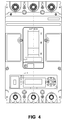
- FIG. 4 illustrates a schematic structural diagram of an electronic circuit equipped with a self-test module of the present invention.
- the self-test module of electronic circuit breaker of the present invention is pluggable.
- the self-test module may be conveniently plugged onto an electronic release. Under non-working status such as manufacturing, installation or maintenance of the electronic circuit breakers, a test of function completeness and reliability of the products may be automatically operated and test results will be provided by pressing a test button on the electronic release, without an extra external accessory.
Landscapes
- Physics & Mathematics (AREA)
- General Physics & Mathematics (AREA)
- Breakers (AREA)
Applications Claiming Priority (2)
| Application Number | Priority Date | Filing Date | Title |
|---|---|---|---|
| CN201310553519.8A CN104635149B (zh) | 2013-11-08 | 2013-11-08 | 电子式断路器的自检模块 |
| PCT/CN2014/089370 WO2015067129A1 (fr) | 2013-11-08 | 2014-10-24 | Module auto-test de disjoncteur électronique |
Publications (3)
| Publication Number | Publication Date |
|---|---|
| EP3067708A1 true EP3067708A1 (fr) | 2016-09-14 |
| EP3067708A4 EP3067708A4 (fr) | 2017-07-19 |
| EP3067708B1 EP3067708B1 (fr) | 2021-09-29 |
Family
ID=53040889
Family Applications (1)
| Application Number | Title | Priority Date | Filing Date |
|---|---|---|---|
| EP14859387.4A Active EP3067708B1 (fr) | 2013-11-08 | 2014-10-24 | Module auto-test de disjoncteur électronique |
Country Status (4)
| Country | Link |
|---|---|
| US (1) | US9797953B2 (fr) |
| EP (1) | EP3067708B1 (fr) |
| CN (1) | CN104635149B (fr) |
| WO (1) | WO2015067129A1 (fr) |
Families Citing this family (9)
| Publication number | Priority date | Publication date | Assignee | Title |
|---|---|---|---|---|
| JP6713291B2 (ja) * | 2016-02-05 | 2020-06-24 | 株式会社デンソーテン | 溶着検知装置及び溶着検知方法 |
| CN105759791B (zh) * | 2016-04-22 | 2018-05-04 | 浙江科能达电气有限公司 | 断路器智能控制器及基于其的实时检测方法 |
| CN107797603B (zh) * | 2017-10-13 | 2023-04-14 | 奥克斯空调股份有限公司 | 一种稳压块的输出电压测试装置 |
| CN110014933A (zh) * | 2018-01-03 | 2019-07-16 | 深圳智链物联科技有限公司 | 充电桩控制电路及充电桩 |
| CN111340319B (zh) * | 2018-11-02 | 2022-04-15 | 北部湾大学 | 板形工件包边系统软件总体流程 |
| CN112067984A (zh) * | 2020-09-03 | 2020-12-11 | 国家电网有限公司 | 一种断路器非全相功能测试装置 |
| CN115833566A (zh) * | 2022-12-07 | 2023-03-21 | 上海锣响汽车集团有限公司 | 一种零待机功耗的遥控器节能控制方法及电路 |
| CN116736090B (zh) * | 2023-08-16 | 2023-11-07 | 深圳市南方硅谷半导体股份有限公司 | 一种临界点不良芯片的测试方法、装置及存储介质 |
| EP4686022A1 (fr) * | 2024-07-24 | 2026-01-28 | Universität Kassel (Körperschaft d. öffentlichen Rechts) | Dispositif de sécurité électrique |
Family Cites Families (24)
| Publication number | Priority date | Publication date | Assignee | Title |
|---|---|---|---|---|
| US3532967A (en) * | 1968-01-23 | 1970-10-06 | Mallory & Co Inc P R | Testing device for circuit breakers and electrical components associated therewith |
| US4105965A (en) * | 1977-07-14 | 1978-08-08 | General Electric Company | Static trip circuit breaker test set |
| JPS58201075A (ja) * | 1982-05-19 | 1983-11-22 | Oki Electric Ind Co Ltd | トランスフアリ−ドスイツチの特性測定回路 |
| US4814712A (en) * | 1987-06-17 | 1989-03-21 | General Electric Company | Test kit for a circuit breaker containing an electronic trip unit |
| US6262871B1 (en) * | 1998-05-28 | 2001-07-17 | X-L Synergy, Llc | Fail safe fault interrupter |
| US6426634B1 (en) * | 1999-03-29 | 2002-07-30 | George A. Spencer | Circuit breaker with integrated self-test enhancements |
| WO2001077698A2 (fr) * | 2000-04-04 | 2001-10-18 | Contact Technology Systems, Inc. | Dispositif d'essai de ligne electrique avec generateur de signal et detecteur de signal |
| US20050002137A1 (en) * | 2003-01-30 | 2005-01-06 | Frantz Germain | Circuit interrupting device with reset lockout and user load test to reset activation |
| US7372678B2 (en) * | 2005-08-24 | 2008-05-13 | Leviton Manufacturing Co., Inc. | Circuit interrupting device with automatic test |
| US7852606B2 (en) * | 2005-08-24 | 2010-12-14 | Leviton Manufacturing Company, Inc. | Self-testing circuit interrupting device |
| US7911746B2 (en) * | 2006-06-01 | 2011-03-22 | Leviton Manufacturing Co., Inc. | GFCI with self-test and remote annunciation capabilities |
| CN201075659Y (zh) * | 2007-09-26 | 2008-06-18 | 上海同铁电子科技有限公司 | 具有自检功能的铁路信号专用智能断路器 |
| CN101910856B (zh) * | 2008-01-29 | 2014-06-18 | 立维腾制造有限公司 | 自测试故障电路中断器装置和方法 |
| US8035936B2 (en) * | 2008-11-18 | 2011-10-11 | Robert Erger | Multiple pole arc-fault circuit breaker using single test button |
| CN201528215U (zh) * | 2009-05-04 | 2010-07-14 | 中兴通讯股份有限公司 | 一种控制电池在线充电的电路 |
| CN202330643U (zh) * | 2011-09-23 | 2012-07-11 | 航天科工防御技术研究试验中心 | 电气元件的电流测试装置 |
| CN202362428U (zh) | 2011-11-24 | 2012-08-01 | 天津市百利电气有限公司 | 低压电器电子脱扣器检测装置 |
| CN202486285U (zh) | 2011-12-23 | 2012-10-10 | 许继集团有限公司 | 一种检测低压成套开关设备回路完整性的测试装置 |
| CN202522680U (zh) * | 2012-04-27 | 2012-11-07 | 西安合电电气有限公司 | 一种断路器检测装置 |
| EP2662697B1 (fr) * | 2012-05-10 | 2014-06-04 | Omicron electronics GmbH | Dispositif de mesure destiné à contrôler un disjoncteur électrique |
| CN202916621U (zh) * | 2012-07-16 | 2013-05-01 | 上海诺雅克电气有限公司 | 一种断路器电子式控制器 |
| CN102968170A (zh) * | 2012-11-28 | 2013-03-13 | 华南理工大学 | 一种计算机智能自保护供电电源 |
| CN103777137B (zh) | 2014-01-15 | 2017-02-15 | 上海诺雅克电气有限公司 | 具有自检功能的电子式断路器及其自诊断方法 |
| CN203786556U (zh) | 2014-01-15 | 2014-08-20 | 上海诺雅克电气有限公司 | 具有自检功能的电子式断路器 |
-
2013
- 2013-11-08 CN CN201310553519.8A patent/CN104635149B/zh active Active
-
2014
- 2014-10-24 WO PCT/CN2014/089370 patent/WO2015067129A1/fr not_active Ceased
- 2014-10-24 EP EP14859387.4A patent/EP3067708B1/fr active Active
- 2014-10-24 US US15/034,674 patent/US9797953B2/en active Active
Also Published As
| Publication number | Publication date |
|---|---|
| US20160274190A1 (en) | 2016-09-22 |
| CN104635149A (zh) | 2015-05-20 |
| EP3067708B1 (fr) | 2021-09-29 |
| WO2015067129A1 (fr) | 2015-05-14 |
| CN104635149B (zh) | 2017-09-05 |
| US9797953B2 (en) | 2017-10-24 |
| EP3067708A4 (fr) | 2017-07-19 |
Similar Documents
| Publication | Publication Date | Title |
|---|---|---|
| US9797953B2 (en) | Self-test module of electronic circuit breaker | |
| US10826286B2 (en) | Battery boost apparatus | |
| CN112366790B (zh) | 智能连接装置、启动电源以及电瓶夹 | |
| CN102570558B (zh) | 一种镍氢镍镉电池的智能充电器及其控制方法 | |
| KR102634126B1 (ko) | 스마트 연결 장치, 시동 전원 및 배터리 클램프 | |
| EP3096430B9 (fr) | Véhicule électrique et circuit d'alimentation pour un dispositif de commande de véhicule avec charge en courant alternatif | |
| US20100254057A1 (en) | Overload power cut-off device and method thereof | |
| KR101455148B1 (ko) | Led 비상등 컨버터 | |
| JP2008271690A (ja) | 二次電池パック | |
| CN101420114A (zh) | 多功能三相电源保护器 | |
| CN214479833U (zh) | 断路器的附件模块及智能控制系统 | |
| CN103777137A (zh) | 具有自检功能的电子式断路器及其自诊断方法 | |
| KR101032468B1 (ko) | 배터리 자동 충전장치 | |
| CN201477140U (zh) | 插座电流显示及警示装置 | |
| CN100372212C (zh) | 具多段电压输出的电源储存装置 | |
| CN103457314A (zh) | 一种开关型单节锂电池充电和升压放电控制芯片 | |
| CN110174608A (zh) | 一种智能电路检测装置 | |
| CN101256705A (zh) | 具有语音和远程提醒控制的设备控制系统报警装置 | |
| CN118825453A (zh) | 锂电转干电电池和锂电转干电电池的控制方法 | |
| CN218449468U (zh) | Pcs保护电路及pcs保护装置 | |
| CN104065043B (zh) | 电池欠压保护和显示电路 | |
| CN215528627U (zh) | 智能连接装置、启动电源以及电瓶夹 | |
| CN204879473U (zh) | 多功能手电筒 | |
| CN203786556U (zh) | 具有自检功能的电子式断路器 | |
| KR101058351B1 (ko) | 레귤레이터와 인버터를 갖는 배터리 충전/방전 제어회로 |
Legal Events
| Date | Code | Title | Description |
|---|---|---|---|
| PUAI | Public reference made under article 153(3) epc to a published international application that has entered the european phase |
Free format text: ORIGINAL CODE: 0009012 |
|
| 17P | Request for examination filed |
Effective date: 20160527 |
|
| AK | Designated contracting states |
Kind code of ref document: A1 Designated state(s): AL AT BE BG CH CY CZ DE DK EE ES FI FR GB GR HR HU IE IS IT LI LT LU LV MC MK MT NL NO PL PT RO RS SE SI SK SM TR |
|
| AX | Request for extension of the european patent |
Extension state: BA ME |
|
| DAX | Request for extension of the european patent (deleted) | ||
| A4 | Supplementary search report drawn up and despatched |
Effective date: 20170619 |
|
| RIC1 | Information provided on ipc code assigned before grant |
Ipc: H02H 1/06 20060101ALI20170609BHEP Ipc: G01R 31/327 20060101AFI20170609BHEP Ipc: H02H 3/04 20060101ALN20170609BHEP |
|
| STAA | Information on the status of an ep patent application or granted ep patent |
Free format text: STATUS: EXAMINATION IS IN PROGRESS |
|
| 17Q | First examination report despatched |
Effective date: 20191125 |
|
| GRAP | Despatch of communication of intention to grant a patent |
Free format text: ORIGINAL CODE: EPIDOSNIGR1 |
|
| STAA | Information on the status of an ep patent application or granted ep patent |
Free format text: STATUS: GRANT OF PATENT IS INTENDED |
|
| INTG | Intention to grant announced |
Effective date: 20210331 |
|
| RIC1 | Information provided on ipc code assigned before grant |
Ipc: H02H 3/04 20060101ALN20210319BHEP Ipc: H02H 1/06 20060101ALI20210319BHEP Ipc: G01R 31/327 20060101AFI20210319BHEP |
|
| INTG | Intention to grant announced |
Effective date: 20210413 |
|
| INTG | Intention to grant announced |
Effective date: 20210415 |
|
| INTG | Intention to grant announced |
Effective date: 20210415 |
|
| GRAS | Grant fee paid |
Free format text: ORIGINAL CODE: EPIDOSNIGR3 |
|
| GRAA | (expected) grant |
Free format text: ORIGINAL CODE: 0009210 |
|
| STAA | Information on the status of an ep patent application or granted ep patent |
Free format text: STATUS: THE PATENT HAS BEEN GRANTED |
|
| AK | Designated contracting states |
Kind code of ref document: B1 Designated state(s): AL AT BE BG CH CY CZ DE DK EE ES FI FR GB GR HR HU IE IS IT LI LT LU LV MC MK MT NL NO PL PT RO RS SE SI SK SM TR |
|
| REG | Reference to a national code |
Ref country code: GB Ref legal event code: FG4D |
|
| REG | Reference to a national code |
Ref country code: DE Ref legal event code: R096 Ref document number: 602014080433 Country of ref document: DE |
|
| REG | Reference to a national code |
Ref country code: CH Ref legal event code: EP Ref country code: AT Ref legal event code: REF Ref document number: 1434650 Country of ref document: AT Kind code of ref document: T Effective date: 20211015 |
|
| REG | Reference to a national code |
Ref country code: IE Ref legal event code: FG4D |
|
| REG | Reference to a national code |
Ref country code: LT Ref legal event code: MG9D |
|
| PG25 | Lapsed in a contracting state [announced via postgrant information from national office to epo] |
Ref country code: SE Free format text: LAPSE BECAUSE OF FAILURE TO SUBMIT A TRANSLATION OF THE DESCRIPTION OR TO PAY THE FEE WITHIN THE PRESCRIBED TIME-LIMIT Effective date: 20210929 Ref country code: RS Free format text: LAPSE BECAUSE OF FAILURE TO SUBMIT A TRANSLATION OF THE DESCRIPTION OR TO PAY THE FEE WITHIN THE PRESCRIBED TIME-LIMIT Effective date: 20210929 Ref country code: HR Free format text: LAPSE BECAUSE OF FAILURE TO SUBMIT A TRANSLATION OF THE DESCRIPTION OR TO PAY THE FEE WITHIN THE PRESCRIBED TIME-LIMIT Effective date: 20210929 Ref country code: LT Free format text: LAPSE BECAUSE OF FAILURE TO SUBMIT A TRANSLATION OF THE DESCRIPTION OR TO PAY THE FEE WITHIN THE PRESCRIBED TIME-LIMIT Effective date: 20210929 Ref country code: BG Free format text: LAPSE BECAUSE OF FAILURE TO SUBMIT A TRANSLATION OF THE DESCRIPTION OR TO PAY THE FEE WITHIN THE PRESCRIBED TIME-LIMIT Effective date: 20211229 Ref country code: NO Free format text: LAPSE BECAUSE OF FAILURE TO SUBMIT A TRANSLATION OF THE DESCRIPTION OR TO PAY THE FEE WITHIN THE PRESCRIBED TIME-LIMIT Effective date: 20211229 Ref country code: FI Free format text: LAPSE BECAUSE OF FAILURE TO SUBMIT A TRANSLATION OF THE DESCRIPTION OR TO PAY THE FEE WITHIN THE PRESCRIBED TIME-LIMIT Effective date: 20210929 |
|
| REG | Reference to a national code |
Ref country code: NL Ref legal event code: MP Effective date: 20210929 |
|
| REG | Reference to a national code |
Ref country code: AT Ref legal event code: MK05 Ref document number: 1434650 Country of ref document: AT Kind code of ref document: T Effective date: 20210929 |
|
| PG25 | Lapsed in a contracting state [announced via postgrant information from national office to epo] |
Ref country code: LV Free format text: LAPSE BECAUSE OF FAILURE TO SUBMIT A TRANSLATION OF THE DESCRIPTION OR TO PAY THE FEE WITHIN THE PRESCRIBED TIME-LIMIT Effective date: 20210929 Ref country code: GR Free format text: LAPSE BECAUSE OF FAILURE TO SUBMIT A TRANSLATION OF THE DESCRIPTION OR TO PAY THE FEE WITHIN THE PRESCRIBED TIME-LIMIT Effective date: 20211230 |
|
| PG25 | Lapsed in a contracting state [announced via postgrant information from national office to epo] |
Ref country code: AT Free format text: LAPSE BECAUSE OF FAILURE TO SUBMIT A TRANSLATION OF THE DESCRIPTION OR TO PAY THE FEE WITHIN THE PRESCRIBED TIME-LIMIT Effective date: 20210929 |
|
| REG | Reference to a national code |
Ref country code: CH Ref legal event code: PL |
|
| PG25 | Lapsed in a contracting state [announced via postgrant information from national office to epo] |
Ref country code: IS Free format text: LAPSE BECAUSE OF FAILURE TO SUBMIT A TRANSLATION OF THE DESCRIPTION OR TO PAY THE FEE WITHIN THE PRESCRIBED TIME-LIMIT Effective date: 20220129 Ref country code: SK Free format text: LAPSE BECAUSE OF FAILURE TO SUBMIT A TRANSLATION OF THE DESCRIPTION OR TO PAY THE FEE WITHIN THE PRESCRIBED TIME-LIMIT Effective date: 20210929 Ref country code: RO Free format text: LAPSE BECAUSE OF FAILURE TO SUBMIT A TRANSLATION OF THE DESCRIPTION OR TO PAY THE FEE WITHIN THE PRESCRIBED TIME-LIMIT Effective date: 20210929 Ref country code: PT Free format text: LAPSE BECAUSE OF FAILURE TO SUBMIT A TRANSLATION OF THE DESCRIPTION OR TO PAY THE FEE WITHIN THE PRESCRIBED TIME-LIMIT Effective date: 20220131 Ref country code: PL Free format text: LAPSE BECAUSE OF FAILURE TO SUBMIT A TRANSLATION OF THE DESCRIPTION OR TO PAY THE FEE WITHIN THE PRESCRIBED TIME-LIMIT Effective date: 20210929 Ref country code: NL Free format text: LAPSE BECAUSE OF FAILURE TO SUBMIT A TRANSLATION OF THE DESCRIPTION OR TO PAY THE FEE WITHIN THE PRESCRIBED TIME-LIMIT Effective date: 20210929 Ref country code: ES Free format text: LAPSE BECAUSE OF FAILURE TO SUBMIT A TRANSLATION OF THE DESCRIPTION OR TO PAY THE FEE WITHIN THE PRESCRIBED TIME-LIMIT Effective date: 20210929 Ref country code: EE Free format text: LAPSE BECAUSE OF FAILURE TO SUBMIT A TRANSLATION OF THE DESCRIPTION OR TO PAY THE FEE WITHIN THE PRESCRIBED TIME-LIMIT Effective date: 20210929 Ref country code: CZ Free format text: LAPSE BECAUSE OF FAILURE TO SUBMIT A TRANSLATION OF THE DESCRIPTION OR TO PAY THE FEE WITHIN THE PRESCRIBED TIME-LIMIT Effective date: 20210929 Ref country code: AL Free format text: LAPSE BECAUSE OF FAILURE TO SUBMIT A TRANSLATION OF THE DESCRIPTION OR TO PAY THE FEE WITHIN THE PRESCRIBED TIME-LIMIT Effective date: 20210929 |
|
| REG | Reference to a national code |
Ref country code: BE Ref legal event code: MM Effective date: 20211031 |
|
| PG25 | Lapsed in a contracting state [announced via postgrant information from national office to epo] |
Ref country code: MC Free format text: LAPSE BECAUSE OF FAILURE TO SUBMIT A TRANSLATION OF THE DESCRIPTION OR TO PAY THE FEE WITHIN THE PRESCRIBED TIME-LIMIT Effective date: 20210929 |
|
| REG | Reference to a national code |
Ref country code: DE Ref legal event code: R097 Ref document number: 602014080433 Country of ref document: DE |
|
| PG25 | Lapsed in a contracting state [announced via postgrant information from national office to epo] |
Ref country code: LU Free format text: LAPSE BECAUSE OF NON-PAYMENT OF DUE FEES Effective date: 20211024 Ref country code: DK Free format text: LAPSE BECAUSE OF FAILURE TO SUBMIT A TRANSLATION OF THE DESCRIPTION OR TO PAY THE FEE WITHIN THE PRESCRIBED TIME-LIMIT Effective date: 20210929 Ref country code: BE Free format text: LAPSE BECAUSE OF NON-PAYMENT OF DUE FEES Effective date: 20211031 |
|
| PLBE | No opposition filed within time limit |
Free format text: ORIGINAL CODE: 0009261 |
|
| STAA | Information on the status of an ep patent application or granted ep patent |
Free format text: STATUS: NO OPPOSITION FILED WITHIN TIME LIMIT |
|
| GBPC | Gb: european patent ceased through non-payment of renewal fee |
Effective date: 20211229 |
|
| PG25 | Lapsed in a contracting state [announced via postgrant information from national office to epo] |
Ref country code: LI Free format text: LAPSE BECAUSE OF NON-PAYMENT OF DUE FEES Effective date: 20211031 Ref country code: CH Free format text: LAPSE BECAUSE OF NON-PAYMENT OF DUE FEES Effective date: 20211031 |
|
| 26N | No opposition filed |
Effective date: 20220630 |
|
| PG25 | Lapsed in a contracting state [announced via postgrant information from national office to epo] |
Ref country code: IE Free format text: LAPSE BECAUSE OF NON-PAYMENT OF DUE FEES Effective date: 20211024 Ref country code: GB Free format text: LAPSE BECAUSE OF NON-PAYMENT OF DUE FEES Effective date: 20211229 |
|
| PG25 | Lapsed in a contracting state [announced via postgrant information from national office to epo] |
Ref country code: SI Free format text: LAPSE BECAUSE OF FAILURE TO SUBMIT A TRANSLATION OF THE DESCRIPTION OR TO PAY THE FEE WITHIN THE PRESCRIBED TIME-LIMIT Effective date: 20210929 Ref country code: FR Free format text: LAPSE BECAUSE OF NON-PAYMENT OF DUE FEES Effective date: 20211129 |
|
| PG25 | Lapsed in a contracting state [announced via postgrant information from national office to epo] |
Ref country code: IT Free format text: LAPSE BECAUSE OF FAILURE TO SUBMIT A TRANSLATION OF THE DESCRIPTION OR TO PAY THE FEE WITHIN THE PRESCRIBED TIME-LIMIT Effective date: 20210929 |
|
| PG25 | Lapsed in a contracting state [announced via postgrant information from national office to epo] |
Ref country code: HU Free format text: LAPSE BECAUSE OF FAILURE TO SUBMIT A TRANSLATION OF THE DESCRIPTION OR TO PAY THE FEE WITHIN THE PRESCRIBED TIME-LIMIT; INVALID AB INITIO Effective date: 20141024 |
|
| PG25 | Lapsed in a contracting state [announced via postgrant information from national office to epo] |
Ref country code: CY Free format text: LAPSE BECAUSE OF FAILURE TO SUBMIT A TRANSLATION OF THE DESCRIPTION OR TO PAY THE FEE WITHIN THE PRESCRIBED TIME-LIMIT Effective date: 20210929 |
|
| PG25 | Lapsed in a contracting state [announced via postgrant information from national office to epo] |
Ref country code: SM Free format text: LAPSE BECAUSE OF FAILURE TO SUBMIT A TRANSLATION OF THE DESCRIPTION OR TO PAY THE FEE WITHIN THE PRESCRIBED TIME-LIMIT Effective date: 20210929 |
|
| PG25 | Lapsed in a contracting state [announced via postgrant information from national office to epo] |
Ref country code: MK Free format text: LAPSE BECAUSE OF FAILURE TO SUBMIT A TRANSLATION OF THE DESCRIPTION OR TO PAY THE FEE WITHIN THE PRESCRIBED TIME-LIMIT Effective date: 20210929 |
|
| PG25 | Lapsed in a contracting state [announced via postgrant information from national office to epo] |
Ref country code: TR Free format text: LAPSE BECAUSE OF FAILURE TO SUBMIT A TRANSLATION OF THE DESCRIPTION OR TO PAY THE FEE WITHIN THE PRESCRIBED TIME-LIMIT Effective date: 20210929 |
|
| PG25 | Lapsed in a contracting state [announced via postgrant information from national office to epo] |
Ref country code: MT Free format text: LAPSE BECAUSE OF FAILURE TO SUBMIT A TRANSLATION OF THE DESCRIPTION OR TO PAY THE FEE WITHIN THE PRESCRIBED TIME-LIMIT Effective date: 20210929 |
|
| PGFP | Annual fee paid to national office [announced via postgrant information from national office to epo] |
Ref country code: DE Payment date: 20250910 Year of fee payment: 12 |