EP3067929A2 - Ensemble de boîtier de semi-conducteur - Google Patents
Ensemble de boîtier de semi-conducteur Download PDFInfo
- Publication number
- EP3067929A2 EP3067929A2 EP16157770.5A EP16157770A EP3067929A2 EP 3067929 A2 EP3067929 A2 EP 3067929A2 EP 16157770 A EP16157770 A EP 16157770A EP 3067929 A2 EP3067929 A2 EP 3067929A2
- Authority
- EP
- European Patent Office
- Prior art keywords
- molding compound
- semiconductor die
- semiconductor package
- package assembly
- rdl
- Prior art date
- Legal status (The legal status is an assumption and is not a legal conclusion. Google has not performed a legal analysis and makes no representation as to the accuracy of the status listed.)
- Ceased
Links
Images


Classifications
-
- H—ELECTRICITY
- H10—SEMICONDUCTOR DEVICES; ELECTRIC SOLID-STATE DEVICES NOT OTHERWISE PROVIDED FOR
- H10W—GENERIC PACKAGES, INTERCONNECTIONS, CONNECTORS OR OTHER CONSTRUCTIONAL DETAILS OF DEVICES COVERED BY CLASS H10
- H10W74/00—Encapsulations, e.g. protective coatings
- H10W74/10—Encapsulations, e.g. protective coatings characterised by their shape or disposition
-
- H—ELECTRICITY
- H10—SEMICONDUCTOR DEVICES; ELECTRIC SOLID-STATE DEVICES NOT OTHERWISE PROVIDED FOR
- H10W—GENERIC PACKAGES, INTERCONNECTIONS, CONNECTORS OR OTHER CONSTRUCTIONAL DETAILS OF DEVICES COVERED BY CLASS H10
- H10W20/00—Interconnections in chips, wafers or substrates
- H10W20/40—Interconnections external to wafers or substrates, e.g. back-end-of-line [BEOL] metallisations or vias connecting to gate electrodes
-
- H—ELECTRICITY
- H10—SEMICONDUCTOR DEVICES; ELECTRIC SOLID-STATE DEVICES NOT OTHERWISE PROVIDED FOR
- H10W—GENERIC PACKAGES, INTERCONNECTIONS, CONNECTORS OR OTHER CONSTRUCTIONAL DETAILS OF DEVICES COVERED BY CLASS H10
- H10W20/00—Interconnections in chips, wafers or substrates
- H10W20/40—Interconnections external to wafers or substrates, e.g. back-end-of-line [BEOL] metallisations or vias connecting to gate electrodes
- H10W20/41—Interconnections external to wafers or substrates, e.g. back-end-of-line [BEOL] metallisations or vias connecting to gate electrodes characterised by their conductive parts
- H10W20/43—Layouts of interconnections
-
- H—ELECTRICITY
- H10—SEMICONDUCTOR DEVICES; ELECTRIC SOLID-STATE DEVICES NOT OTHERWISE PROVIDED FOR
- H10W—GENERIC PACKAGES, INTERCONNECTIONS, CONNECTORS OR OTHER CONSTRUCTIONAL DETAILS OF DEVICES COVERED BY CLASS H10
- H10W70/00—Package substrates; Interposers; Redistribution layers [RDL]
- H10W70/01—Manufacture or treatment
- H10W70/05—Manufacture or treatment of insulating or insulated package substrates, or of interposers, or of redistribution layers
- H10W70/08—Manufacture or treatment of insulating or insulated package substrates, or of interposers, or of redistribution layers by depositing layers on the chip or wafer, e.g. "chip-first" RDLs
- H10W70/09—Manufacture or treatment of insulating or insulated package substrates, or of interposers, or of redistribution layers by depositing layers on the chip or wafer, e.g. "chip-first" RDLs extending onto an encapsulation that laterally surrounds the chip or wafer, e.g. fan-out wafer level package [FOWLP] RDLs
-
- H—ELECTRICITY
- H10—SEMICONDUCTOR DEVICES; ELECTRIC SOLID-STATE DEVICES NOT OTHERWISE PROVIDED FOR
- H10W—GENERIC PACKAGES, INTERCONNECTIONS, CONNECTORS OR OTHER CONSTRUCTIONAL DETAILS OF DEVICES COVERED BY CLASS H10
- H10W70/00—Package substrates; Interposers; Redistribution layers [RDL]
- H10W70/60—Insulating or insulated package substrates; Interposers; Redistribution layers
- H10W70/611—Insulating or insulated package substrates; Interposers; Redistribution layers for connecting multiple chips together
-
- H—ELECTRICITY
- H10—SEMICONDUCTOR DEVICES; ELECTRIC SOLID-STATE DEVICES NOT OTHERWISE PROVIDED FOR
- H10W—GENERIC PACKAGES, INTERCONNECTIONS, CONNECTORS OR OTHER CONSTRUCTIONAL DETAILS OF DEVICES COVERED BY CLASS H10
- H10W70/00—Package substrates; Interposers; Redistribution layers [RDL]
- H10W70/60—Insulating or insulated package substrates; Interposers; Redistribution layers
- H10W70/611—Insulating or insulated package substrates; Interposers; Redistribution layers for connecting multiple chips together
- H10W70/614—Insulating or insulated package substrates; Interposers; Redistribution layers for connecting multiple chips together the multiple chips being integrally enclosed
-
- H—ELECTRICITY
- H10—SEMICONDUCTOR DEVICES; ELECTRIC SOLID-STATE DEVICES NOT OTHERWISE PROVIDED FOR
- H10W—GENERIC PACKAGES, INTERCONNECTIONS, CONNECTORS OR OTHER CONSTRUCTIONAL DETAILS OF DEVICES COVERED BY CLASS H10
- H10W74/00—Encapsulations, e.g. protective coatings
- H10W74/01—Manufacture or treatment
- H10W74/019—Manufacture or treatment using temporary auxiliary substrates
-
- H—ELECTRICITY
- H10—SEMICONDUCTOR DEVICES; ELECTRIC SOLID-STATE DEVICES NOT OTHERWISE PROVIDED FOR
- H10W—GENERIC PACKAGES, INTERCONNECTIONS, CONNECTORS OR OTHER CONSTRUCTIONAL DETAILS OF DEVICES COVERED BY CLASS H10
- H10W90/00—Package configurations
-
- H—ELECTRICITY
- H10—SEMICONDUCTOR DEVICES; ELECTRIC SOLID-STATE DEVICES NOT OTHERWISE PROVIDED FOR
- H10W—GENERIC PACKAGES, INTERCONNECTIONS, CONNECTORS OR OTHER CONSTRUCTIONAL DETAILS OF DEVICES COVERED BY CLASS H10
- H10W90/00—Package configurations
- H10W90/401—Package configurations characterised by multiple insulating or insulated package substrates, interposers or RDLs
-
- H—ELECTRICITY
- H10—SEMICONDUCTOR DEVICES; ELECTRIC SOLID-STATE DEVICES NOT OTHERWISE PROVIDED FOR
- H10W—GENERIC PACKAGES, INTERCONNECTIONS, CONNECTORS OR OTHER CONSTRUCTIONAL DETAILS OF DEVICES COVERED BY CLASS H10
- H10W70/00—Package substrates; Interposers; Redistribution layers [RDL]
- H10W70/099—Connecting interconnections to insulating or insulated package substrates, interposers or redistribution layers
-
- H—ELECTRICITY
- H10—SEMICONDUCTOR DEVICES; ELECTRIC SOLID-STATE DEVICES NOT OTHERWISE PROVIDED FOR
- H10W—GENERIC PACKAGES, INTERCONNECTIONS, CONNECTORS OR OTHER CONSTRUCTIONAL DETAILS OF DEVICES COVERED BY CLASS H10
- H10W72/00—Interconnections or connectors in packages
- H10W72/071—Connecting or disconnecting
- H10W72/072—Connecting or disconnecting of bump connectors
-
- H—ELECTRICITY
- H10—SEMICONDUCTOR DEVICES; ELECTRIC SOLID-STATE DEVICES NOT OTHERWISE PROVIDED FOR
- H10W—GENERIC PACKAGES, INTERCONNECTIONS, CONNECTORS OR OTHER CONSTRUCTIONAL DETAILS OF DEVICES COVERED BY CLASS H10
- H10W72/00—Interconnections or connectors in packages
- H10W72/20—Bump connectors, e.g. solder bumps or copper pillars; Dummy bumps; Thermal bumps
- H10W72/241—Dispositions, e.g. layouts
-
- H—ELECTRICITY
- H10—SEMICONDUCTOR DEVICES; ELECTRIC SOLID-STATE DEVICES NOT OTHERWISE PROVIDED FOR
- H10W—GENERIC PACKAGES, INTERCONNECTIONS, CONNECTORS OR OTHER CONSTRUCTIONAL DETAILS OF DEVICES COVERED BY CLASS H10
- H10W72/00—Interconnections or connectors in packages
- H10W72/20—Bump connectors, e.g. solder bumps or copper pillars; Dummy bumps; Thermal bumps
- H10W72/251—Materials
- H10W72/252—Materials comprising solid metals or solid metalloids, e.g. PbSn, Ag or Cu
-
- H—ELECTRICITY
- H10—SEMICONDUCTOR DEVICES; ELECTRIC SOLID-STATE DEVICES NOT OTHERWISE PROVIDED FOR
- H10W—GENERIC PACKAGES, INTERCONNECTIONS, CONNECTORS OR OTHER CONSTRUCTIONAL DETAILS OF DEVICES COVERED BY CLASS H10
- H10W72/00—Interconnections or connectors in packages
- H10W72/851—Dispositions of multiple connectors or interconnections
- H10W72/853—On the same surface
-
- H—ELECTRICITY
- H10—SEMICONDUCTOR DEVICES; ELECTRIC SOLID-STATE DEVICES NOT OTHERWISE PROVIDED FOR
- H10W—GENERIC PACKAGES, INTERCONNECTIONS, CONNECTORS OR OTHER CONSTRUCTIONAL DETAILS OF DEVICES COVERED BY CLASS H10
- H10W72/00—Interconnections or connectors in packages
- H10W72/90—Bond pads, in general
- H10W72/941—Dispositions of bond pads
- H10W72/9413—Dispositions of bond pads on encapsulations
-
- H—ELECTRICITY
- H10—SEMICONDUCTOR DEVICES; ELECTRIC SOLID-STATE DEVICES NOT OTHERWISE PROVIDED FOR
- H10W—GENERIC PACKAGES, INTERCONNECTIONS, CONNECTORS OR OTHER CONSTRUCTIONAL DETAILS OF DEVICES COVERED BY CLASS H10
- H10W74/00—Encapsulations, e.g. protective coatings
- H10W74/10—Encapsulations, e.g. protective coatings characterised by their shape or disposition
- H10W74/15—Encapsulations, e.g. protective coatings characterised by their shape or disposition on active surfaces of flip-chip devices, e.g. underfills
-
- H—ELECTRICITY
- H10—SEMICONDUCTOR DEVICES; ELECTRIC SOLID-STATE DEVICES NOT OTHERWISE PROVIDED FOR
- H10W—GENERIC PACKAGES, INTERCONNECTIONS, CONNECTORS OR OTHER CONSTRUCTIONAL DETAILS OF DEVICES COVERED BY CLASS H10
- H10W90/00—Package configurations
- H10W90/20—Configurations of stacked chips
- H10W90/271—Configurations of stacked chips the chips having passive surfaces facing each other, i.e. in a back-to-back arrangement
-
- H—ELECTRICITY
- H10—SEMICONDUCTOR DEVICES; ELECTRIC SOLID-STATE DEVICES NOT OTHERWISE PROVIDED FOR
- H10W—GENERIC PACKAGES, INTERCONNECTIONS, CONNECTORS OR OTHER CONSTRUCTIONAL DETAILS OF DEVICES COVERED BY CLASS H10
- H10W90/00—Package configurations
- H10W90/20—Configurations of stacked chips
- H10W90/291—Configurations of stacked chips characterised by containers, encapsulations, or other housings for the stacked chips
-
- H—ELECTRICITY
- H10—SEMICONDUCTOR DEVICES; ELECTRIC SOLID-STATE DEVICES NOT OTHERWISE PROVIDED FOR
- H10W—GENERIC PACKAGES, INTERCONNECTIONS, CONNECTORS OR OTHER CONSTRUCTIONAL DETAILS OF DEVICES COVERED BY CLASS H10
- H10W90/00—Package configurations
- H10W90/701—Package configurations characterised by the relative positions of pads or connectors relative to package parts
- H10W90/721—Package configurations characterised by the relative positions of pads or connectors relative to package parts of bump connectors
- H10W90/722—Package configurations characterised by the relative positions of pads or connectors relative to package parts of bump connectors between stacked chips
-
- H—ELECTRICITY
- H10—SEMICONDUCTOR DEVICES; ELECTRIC SOLID-STATE DEVICES NOT OTHERWISE PROVIDED FOR
- H10W—GENERIC PACKAGES, INTERCONNECTIONS, CONNECTORS OR OTHER CONSTRUCTIONAL DETAILS OF DEVICES COVERED BY CLASS H10
- H10W90/00—Package configurations
- H10W90/701—Package configurations characterised by the relative positions of pads or connectors relative to package parts
- H10W90/721—Package configurations characterised by the relative positions of pads or connectors relative to package parts of bump connectors
- H10W90/724—Package configurations characterised by the relative positions of pads or connectors relative to package parts of bump connectors between a chip and a stacked insulating package substrate, interposer or RDL
-
- H—ELECTRICITY
- H10—SEMICONDUCTOR DEVICES; ELECTRIC SOLID-STATE DEVICES NOT OTHERWISE PROVIDED FOR
- H10W—GENERIC PACKAGES, INTERCONNECTIONS, CONNECTORS OR OTHER CONSTRUCTIONAL DETAILS OF DEVICES COVERED BY CLASS H10
- H10W90/00—Package configurations
- H10W90/701—Package configurations characterised by the relative positions of pads or connectors relative to package parts
- H10W90/721—Package configurations characterised by the relative positions of pads or connectors relative to package parts of bump connectors
- H10W90/728—Package configurations characterised by the relative positions of pads or connectors relative to package parts of bump connectors between a chip and a stacked discrete passive device, e.g. resistors, capacitors or inductors
-
- H—ELECTRICITY
- H10—SEMICONDUCTOR DEVICES; ELECTRIC SOLID-STATE DEVICES NOT OTHERWISE PROVIDED FOR
- H10W—GENERIC PACKAGES, INTERCONNECTIONS, CONNECTORS OR OTHER CONSTRUCTIONAL DETAILS OF DEVICES COVERED BY CLASS H10
- H10W90/00—Package configurations
- H10W90/701—Package configurations characterised by the relative positions of pads or connectors relative to package parts
- H10W90/731—Package configurations characterised by the relative positions of pads or connectors relative to package parts of die-attach connectors
- H10W90/738—Package configurations characterised by the relative positions of pads or connectors relative to package parts of die-attach connectors between a chip and a stacked discrete passive device
Definitions
- the present invention relates to a semiconductor package assembly, and in particular to a semiconductor package assembly with a passive device.
- semiconductor packages be small in size, to support multi-pin connection, high speeds, and high functionality.
- the multi-functional semiconductor package usually requires that passive devices be integrated therein.
- passive devices it is hard to provide additional area for the passive devices mounted thereon.
- a semiconductor package assembly is provided.
- An exemplary embodiment of a semiconductor package assembly includes a semiconductor die.
- a first molding compound covers a back surface of the semiconductor die.
- a redistribution layer (RDL) structure is disposed on a front surface of the semiconductor die.
- the semiconductor die is coupled to the RDL structure.
- a second molding compound is disposed on the front surface of the semiconductor die and embedded in the RDL structure.
- a passive device is disposed on the second molding compound and coupled to the semiconductor die.
- a first molding compound is disposed on a first surface of the semiconductor die.
- a redistribution layer (RDL) structure is disposed on a second surface opposite the first surface of the semiconductor die.
- a second molding compound is disposed on the second surface of the semiconductor die and embedded in the redistribution layer (RDL) structure. The second molding compound is separated from the first molding compound through the redistribution layer (RDL) structure.
- a passive device is disposed on the second molding compound and coupled to the semiconductor die.
- Yet another exemplary embodiment of a semiconductor package assembly includes a semiconductor die.
- a first molding compound is in contact with a first surface of the semiconductor die.
- a redistribution layer (RDL) structure covers a first portion of a second surface opposite the first surface of the semiconductor die.
- a second molding compound covers a second portion of the second surface of the semiconductor die and embedded in the RDL structure.
- a passive device covers the second portion of the second surface of the semiconductor die. The second molding compound is disposed between the semiconductor die and the passive device.
- RDL redistribution layer
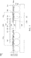
- FIG. 1 is a cross-sectional view of a semiconductor package assembly 500a in accordance with some embodiments of the disclosure.
- the semiconductor package assembly 500a is a wafer-level semiconductor package assembly, for example, a flip-chip semiconductor package assembly. To clearly show the arrangement of a passive device and conductive structures of the semiconductor package assembly, the size of the passive device and the size of conductive structures are enlarged.
- the semiconductor package assembly 500a includes at least one wafer-level semiconductor package 350a mounted on a base 200.
- the wafer-level semiconductor package 350a includes a system-on-chip (SOC) package.
- the base 200 for example a printed circuit board (PCB), may be formed of polypropylene (PP). It should also be noted that the base 200 can be a single layer or a multilayer structure.
- a plurality of pads (not shown) and/or conductive traces (not shown) is disposed on a die-attach surface 202 of the base 200.
- the conductive traces may comprise power segments, signal trace segments or ground trace segments, which are used for the input/output (I/O) connections of the wafer-level semiconductor package 350a.
- the wafer-level semiconductor package 350a is mounted directly on the conductive traces.
- the pads are disposed on the die-attach surface 202, connected to different terminals of the conductive traces. The pads are used for the wafer-level semiconductor package 350a mounted directly thereon.
- the wafer-level semiconductor package 350a is mounted on the die-attach surface 202 of the base 200 by a bonding process.
- the wafer-level semiconductor package 350a is mounted on the base 200 through the conductive structures 332.
- the wafer-level semiconductor package 350a includes a semiconductor die 300 and a redistribution layer (RDL) structure 310.
- the semiconductor die 300 for example, a system-on-chip (SOC) die, may include a logic die including a central processing unit (CPU), a graphics processing unit (GPU), a dynamic random access memory (DRAM) controller or any combination thereof.
- CPU central processing unit
- GPU graphics processing unit
- DRAM dynamic random access memory
- pads 308 of the semiconductor die 300 are disposed on the front surface 302 to be electrically connected to the circuitry (not shown) of the semiconductor die 300.
- the pads 308 belong to the uppermost metal layer of the interconnection structure (not shown) of the semiconductor die 300.
- the pads 308 of the semiconductor die 300 It should be noted that the number of semiconductor dies 300 integrated in the semiconductor package assembly 500a is not limited to that disclosed in the embodiment.
- the wafer-level semiconductor package 350a further includes a first molding compound 360 covering and surrounding the semiconductor die 300.
- the first molding compound 360 is disposed on and in contact with a back surface 304 and sidewall surface 306 of the semiconductor die 300.
- the first molding compound 360 may be formed of a nonconductive material, such as an epoxy, a resin, a moldable polymer, or the like.
- the first molding compound 360 may be applied while substantially liquid, and then may be cured through a chemical reaction, such as in an epoxy or resin.
- the first molding compound 360 may be an ultraviolet (UV) or thermally cured polymer applied as a gel or malleable solid capable of being disposed around the semiconductor die 300, and then may be cured through a UV or thermal curing process.
- the first molding compound 360 may be cured with a mold (not shown).
- the first molding compound 360 may be replaced by underfill layer.
- the wafer-level semiconductor package 350a further includes a redistribution layer (RDL) structure 310 disposed on the front surface 302 of the semiconductor die 300.
- the RDL structure 310 has opposite surfaces 312 and 314.
- the RDL structure 310 may have one or more conductive traces 316 disposed in one or more inter-metal dielectric (IMD) layers 318.
- the semiconductor die 300 is connected to the conductive traces 316 close to the central portion of the surface 314.
- the first molding compound 360 covers the surface 314 of the RDL structure 310.
- the first molding compound 360 is in contact with the periphery portion of the surface 314, which surrounds the central portion of the surface 314.
- the number of conductive traces 316 and the number of IMD layers 318 of the RDL structure 310 shown in FIG. 1 is only an example and is not a limitation to the present invention.
- the wafer-level semiconductor package 350a further includes conductive structures 332 disposed on the surface 312 of the RDL structure 310, which is away from the semiconductor die 300.
- the conductive structures 332 are coupled to the conductive traces 316 through pads 328, which is disposed on the conductive traces 316 and close to the surface 312.
- the conductive structures 332 are separated from the first molding compound 360 through the RDL structure 310. In other words, the conductive structures 332 are free from in contact with the first molding compound 360.
- the conductive structures 332 may comprise a conductive bump structure such as a copper bump or a solder bump structure, a conductive pillar structure, a conductive wire structure, or a conductive paste structure.
- the wafer-level semiconductor package 350a further includes a second molding compound 320 disposed on the front surface 302 of the semiconductor die 300.
- the molding compound 320 includes a surface 321a close to the semiconductor die 300 and a surface 321b opposite from the surface 321a.
- the RDL structure 310 and the second molding compound 320 cover different respective portions of the front surface 302 of the semiconductor die 300.
- the RDL structure 310 covers a portion 302a of the front surface 302 of the semiconductor die 300.
- the second molding compound 320 covers a portion 302b of the front surface 302 of the semiconductor die 300.
- the portion 302a is adjacent to the portion 302b.
- the second molding compound 320 is embedded in the RDL structure 310.
- a sidewall 322 of the second molding compound 320 is surrounded by the RDL structure 310. Also, the second molding compound 320 is separated from the first molding compound 360 through the semiconductor die 300 and the RDL structure 310. In some embodiments, the materials and the manufacturing processes of the second molding compound 320 may be similar to those of the first molding compound 360.
- the wafer-level semiconductor package 350a further includes a passive device 330, for example, a decoupling capacitor, disposed on the second molding compound 320.
- the passive device 330 may comprise a passive device chip or a discrete passive device, for example, a multilayer ceramic chip capacitor (MLCC) device, or integrated passive device (IPD).
- the passive device 330 and the conductive structures 332 are disposed close to the surface 312 of the RDL structure 310, which is away from the semiconductor die 300 as shown in FIG. 1 .
- an interface i.e. the surface 321b of the second molding compound 320
- the passive device 330 and the second molding compound 320 is aligned to the surface 312 of the RDL structure 310, which is away from the semiconductor die 300.
- the passive device 330 is coupled to the semiconductor die 300 through conductive bumps 324 and solders 326 as shown in FIG. 1 .
- the conductive bumps 324 are formed passing through the second molding compound 320. Also, the conductive bumps 324 are in contact with terminals (not shown) of the passive device 330.
- the solders 326 are disposed between and in contact with the corresponding conductive bumps 324 and the corresponding pads 308 of the semiconductor die 300. In some embodiments, the conductive bumps 324 and the solders 326 are surrounded by the second molding compound 320. Therefore, the conductive bumps 324 and the solders 326 are electrically isolated form the RDL structure 310 by the second molding compound 320.
- the conductive bumps 324 may include copper bumps or copper pillars.
- the passive device 330 is coupled to the semiconductor die 300 without using the conductive traces 316 of the RDL structure 310. Therefore, the length of the electrically conductive path between the passive device 330 and the semiconductor die 300 (i.e. the lengths of the conductive bump 324 and the corresponding solder 326 in this embodiment) can be reduced further to improve signal integrity/power integrity (SI/PI) performance of the of the semiconductor package assembly 500a.
- SI/PI signal integrity/power integrity
- the thickness (height) of the passive device 330 is designed to be less than the diameter of the conductive structures 332 as shown in FIG. 1 .
- the thin profile of the passive device 330 may facilitate processing the surface-mount technology (SMT) rework process for the conductive structures 332 of the wafer-level semiconductor package 350a.
- SMT surface-mount technology
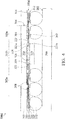
- FIG. 2 is a cross-sectional view of a semiconductor package assembly 500b in accordance with some embodiments of the disclosure. Descriptions of elements of the embodiments hereinafter that are the same or similar as those previously described with reference to FIG. 1 are omitted for brevity.
- one of the differences between the semiconductor package assembly 500a shown in FIG. 1 and the semiconductor package assembly 500b is that a portion of the passive device 330 of the semiconductor package 350b is embedded in the RDL structure 310.
- the interface i.e. the surface 321b of the second molding compound 320
- the passive device 330 and the second molding compound 320 is between the opposite surfaces 312 and 314 of the RDL structure 310 of the wafer-level semiconductor package 350b of the semiconductor package assembly 500b.
- the thickness (height) the passive device 330 above the surface 312 of the RDL structure 310 is less than the diameter of the conductive structures 332 as shown in FIG. 2 .
- the thin profile of the passive device 330 may facilitate processing the surface-mount technology (SMT) rework process for the conductive structures 332 of the wafer-level semiconductor package 350b.
- SMT surface-mount technology
- FIG. 3 is a cross-sectional view of a semiconductor package assembly 500c in accordance with some embodiments of the disclosure. Descriptions of elements of the embodiments hereinafter that are the same or similar as those previously described with reference to FIGS. 1-2 are omitted for brevity.
- one of the differences between the semiconductor package assembly 500a shown in FIG. 1 and the semiconductor package assembly 500c is that the passive device 330 of a semiconductor package 350c is coupled to the solders 326 without using any conductive bump.
- the semiconductor package 350c is in direct contact with the solders 326.
- an interface i.e. the position of the surface 321b of the second molding compound 320
- the passive device 330 and the second molding compound 320 is between the opposite surfaces 312 and 314 of the RDL structure 310 of the wafer-level semiconductor package 350c of the semiconductor package assembly 500c.
- the thickness (height) the passive device 330 above the surface 312 of the RDL structure 310 is much less than the diameter of the conductive structures 332 as shown in FIG. 3 .
- the thin profile of the passive device 330 may facilitate processing the surface-mount technology (SMT) rework process for the conductive structures 332 of the wafer-level semiconductor package 350c.
- SMT surface-mount technology
- FIG. 4 is a cross-sectional view of a semiconductor package assembly 500d in accordance with some embodiments of the disclosure. Descriptions of elements of the embodiments hereinafter that are the same or similar as those previously described with reference to FIGS. 1-3 are omitted for brevity.
- one of the differences between the semiconductor package assembly 500a shown in FIG. 1 and the semiconductor package assembly 500d is that some of the conductive traces 316 of the RDL structure 310 may be formed extending into the second molding compound 320. It should be noted that the conductive traces 316 extended into the second molding compound 320 are electrically isolated from the conductive bumps 324 and the solders 326 through the second molding compound 320.
- Embodiments provide a semiconductor package assembly.
- the semiconductor package assembly includes a wafer-level semiconductor package.
- the wafer-level semiconductor package includes a semiconductor die.
- a first molding compound covers a back surface of the semiconductor die.
- a redistribution layer (RDL) structure is disposed on a front surface of the semiconductor die.
- the semiconductor die is coupled to the RDL structure.
- a second molding compound is disposed on the front surface of the semiconductor die and embedded in the RDL structure.
- a passive device is disposed on the second molding compound and coupled to the semiconductor die.
- the passive device and conductive structures e.g. solder ball or bump structures
- the passive device is coupled to the semiconductor die through conductive bumps passing through the second molding compound.
- the RDL structure and the second molding compound cover different portions of the front surface of the semiconductor die, respectively.
- the passive device is coupled to the semiconductor die without using conductive traces of the RDL structure. Therefore, the length of the electrically conductive path between the passive device and the semiconductor die (i.e. the length of the conductive bump) can be reduced further to improve signal integrity/power integrity (SI/PI) performance of the of the semiconductor package assembly.
- the thickness (height) of the passive device is designed to be less than the diameter of the conductive structures.
- the thin profile of the passive device may facilitate processing the surface-mount technology (SMT) rework process for the conductive structures of the wafer-level semiconductor package.
- the passive device of the wafer-level semiconductor package is designed to be embedded in a portion of the RDL structure to further reduce the distance between the passive device and the semiconductor die.
Landscapes
- Structures Or Materials For Encapsulating Or Coating Semiconductor Devices Or Solid State Devices (AREA)
- Engineering & Computer Science (AREA)
- Manufacturing & Machinery (AREA)
- Production Of Multi-Layered Print Wiring Board (AREA)
Applications Claiming Priority (2)
| Application Number | Priority Date | Filing Date | Title |
|---|---|---|---|
| US201562132677P | 2015-03-13 | 2015-03-13 | |
| US15/014,604 US9711488B2 (en) | 2015-03-13 | 2016-02-03 | Semiconductor package assembly |
Publications (2)
| Publication Number | Publication Date |
|---|---|
| EP3067929A2 true EP3067929A2 (fr) | 2016-09-14 |
| EP3067929A3 EP3067929A3 (fr) | 2016-11-23 |
Family
ID=55446688
Family Applications (1)
| Application Number | Title | Priority Date | Filing Date |
|---|---|---|---|
| EP16157770.5A Ceased EP3067929A3 (fr) | 2015-03-13 | 2016-02-29 | Ensemble de boîtier de semi-conducteur |
Country Status (4)
| Country | Link |
|---|---|
| US (2) | US9711488B2 (fr) |
| EP (1) | EP3067929A3 (fr) |
| CN (1) | CN105977220B (fr) |
| TW (1) | TWI618223B (fr) |
Families Citing this family (8)
| Publication number | Priority date | Publication date | Assignee | Title |
|---|---|---|---|---|
| US9711488B2 (en) * | 2015-03-13 | 2017-07-18 | Mediatek Inc. | Semiconductor package assembly |
| US20170084594A1 (en) * | 2015-09-20 | 2017-03-23 | Qualcomm Incorporated | Embedding die technology |
| US10366968B2 (en) * | 2016-09-30 | 2019-07-30 | Intel IP Corporation | Interconnect structure for a microelectronic device |
| CN106876290A (zh) | 2017-03-10 | 2017-06-20 | 三星半导体(中国)研究开发有限公司 | 晶圆级扇出型封装件及其制造方法 |
| KR102767455B1 (ko) * | 2020-01-20 | 2025-02-14 | 삼성전자주식회사 | 차단층을 포함하는 반도체 패키지 |
| TWI759213B (zh) * | 2020-07-10 | 2022-03-21 | 大陸商廣州印芯半導體技術有限公司 | 光感測器及其感測方法 |
| US20230011666A1 (en) * | 2021-07-09 | 2023-01-12 | Mediatek Singapore Pte. Ltd. | Semiconductor package structure |
| KR102891038B1 (ko) * | 2023-08-29 | 2025-11-28 | (주)피코셈 | 반도체 디바이스 및 그 제조 방법 |
Family Cites Families (12)
| Publication number | Priority date | Publication date | Assignee | Title |
|---|---|---|---|---|
| JP3792445B2 (ja) * | 1999-03-30 | 2006-07-05 | 日本特殊陶業株式会社 | コンデンサ付属配線基板 |
| JP5000071B2 (ja) * | 2003-02-26 | 2012-08-15 | 新光電気工業株式会社 | 半導体装置用基板及び半導体装置 |
| JP4865197B2 (ja) * | 2004-06-30 | 2012-02-01 | ルネサスエレクトロニクス株式会社 | 半導体装置およびその製造方法 |
| US8367470B2 (en) | 2009-08-07 | 2013-02-05 | Stats Chippac, Ltd. | Semiconductor device and method of forming cavity in build-up interconnect structure for short signal path between die |
| US8519537B2 (en) * | 2010-02-26 | 2013-08-27 | Taiwan Semiconductor Manufacturing Company, Ltd. | 3D semiconductor package interposer with die cavity |
| US9385095B2 (en) * | 2010-02-26 | 2016-07-05 | Taiwan Semiconductor Manufacturing Company, Ltd. | 3D semiconductor package interposer with die cavity |
| CN102169875B (zh) * | 2010-02-26 | 2013-04-17 | 台湾积体电路制造股份有限公司 | 半导体装置及其制造方法 |
| US8618654B2 (en) * | 2010-07-20 | 2013-12-31 | Marvell World Trade Ltd. | Structures embedded within core material and methods of manufacturing thereof |
| US8455995B2 (en) * | 2010-04-16 | 2013-06-04 | Taiwan Semiconductor Manufacturing Company, Ltd. | TSVs with different sizes in interposers for bonding dies |
| US8866301B2 (en) * | 2010-05-18 | 2014-10-21 | Taiwan Semiconductor Manufacturing Company, Ltd. | Package systems having interposers with interconnection structures |
| US9478474B2 (en) * | 2012-12-28 | 2016-10-25 | Taiwan Semiconductor Manufacturing Company, Ltd. | Methods and apparatus for forming package-on-packages |
| US9711488B2 (en) * | 2015-03-13 | 2017-07-18 | Mediatek Inc. | Semiconductor package assembly |
-
2016
- 2016-02-03 US US15/014,604 patent/US9711488B2/en active Active
- 2016-02-29 EP EP16157770.5A patent/EP3067929A3/fr not_active Ceased
- 2016-03-09 TW TW105107160A patent/TWI618223B/zh not_active IP Right Cessation
- 2016-03-10 CN CN201610135933.0A patent/CN105977220B/zh active Active
-
2017
- 2017-06-16 US US15/624,790 patent/US9997498B2/en active Active
Non-Patent Citations (1)
| Title |
|---|
| None |
Also Published As
| Publication number | Publication date |
|---|---|
| CN105977220A (zh) | 2016-09-28 |
| TW201705444A (zh) | 2017-02-01 |
| TWI618223B (zh) | 2018-03-11 |
| US20160268234A1 (en) | 2016-09-15 |
| US20170287877A1 (en) | 2017-10-05 |
| US9997498B2 (en) | 2018-06-12 |
| CN105977220B (zh) | 2018-10-12 |
| US9711488B2 (en) | 2017-07-18 |
| EP3067929A3 (fr) | 2016-11-23 |
Similar Documents
| Publication | Publication Date | Title |
|---|---|---|
| US9978729B2 (en) | Semiconductor package assembly | |
| US10217724B2 (en) | Semiconductor package assembly with embedded IPD | |
| US10177125B2 (en) | Semiconductor package assembly | |
| US9997498B2 (en) | Semiconductor package assembly | |
| EP3007225B1 (fr) | Ensemble de boîtier de semi-conducteur | |
| US10679949B2 (en) | Semiconductor package assembly with redistribution layer (RDL) trace | |
| EP3091571A2 (fr) | Ensemble de boîtier de semi-conducteur avec une antenne incorporé | |
| US20160079205A1 (en) | Semiconductor package assembly | |
| US10147674B2 (en) | Semiconductor package assembly | |
| US10497678B2 (en) | Semiconductor package assembly with passive device | |
| CN105845639A (zh) | 电子封装结构及导电结构 | |
| US20170141041A1 (en) | Semiconductor package assembly | |
| US20180315678A1 (en) | Package structure and method of fabricating the same | |
| US20160163629A1 (en) | Semiconductor package and method of fabricating the same |
Legal Events
| Date | Code | Title | Description |
|---|---|---|---|
| PUAI | Public reference made under article 153(3) epc to a published international application that has entered the european phase |
Free format text: ORIGINAL CODE: 0009012 |
|
| AK | Designated contracting states |
Kind code of ref document: A2 Designated state(s): AL AT BE BG CH CY CZ DE DK EE ES FI FR GB GR HR HU IE IS IT LI LT LU LV MC MK MT NL NO PL PT RO RS SE SI SK SM TR |
|
| AX | Request for extension of the european patent |
Extension state: BA ME |
|
| PUAL | Search report despatched |
Free format text: ORIGINAL CODE: 0009013 |
|
| AK | Designated contracting states |
Kind code of ref document: A3 Designated state(s): AL AT BE BG CH CY CZ DE DK EE ES FI FR GB GR HR HU IE IS IT LI LT LU LV MC MK MT NL NO PL PT RO RS SE SI SK SM TR |
|
| AX | Request for extension of the european patent |
Extension state: BA ME |
|
| RIC1 | Information provided on ipc code assigned before grant |
Ipc: H01L 25/16 20060101AFI20161018BHEP |
|
| 17P | Request for examination filed |
Effective date: 20170505 |
|
| RBV | Designated contracting states (corrected) |
Designated state(s): AL AT BE BG CH CY CZ DE DK EE ES FI FR GB GR HR HU IE IS IT LI LT LU LV MC MK MT NL NO PL PT RO RS SE SI SK SM TR |
|
| 17Q | First examination report despatched |
Effective date: 20170913 |
|
| STAA | Information on the status of an ep patent application or granted ep patent |
Free format text: STATUS: THE APPLICATION HAS BEEN REFUSED |
|
| 18R | Application refused |
Effective date: 20190430 |