EP3067937B1 - Solarzellenmodul - Google Patents
Solarzellenmodul Download PDFInfo
- Publication number
- EP3067937B1 EP3067937B1 EP16159847.9A EP16159847A EP3067937B1 EP 3067937 B1 EP3067937 B1 EP 3067937B1 EP 16159847 A EP16159847 A EP 16159847A EP 3067937 B1 EP3067937 B1 EP 3067937B1
- Authority
- EP
- European Patent Office
- Prior art keywords
- solar cell
- light reflection
- reflection member
- cell module
- thickness
- Prior art date
- Legal status (The legal status is an assumption and is not a legal conclusion. Google has not performed a legal analysis and makes no representation as to the accuracy of the status listed.)
- Not-in-force
Links
Images







Classifications
-
- H—ELECTRICITY
- H10—SEMICONDUCTOR DEVICES; ELECTRIC SOLID-STATE DEVICES NOT OTHERWISE PROVIDED FOR
- H10F—INORGANIC SEMICONDUCTOR DEVICES SENSITIVE TO INFRARED RADIATION, LIGHT, ELECTROMAGNETIC RADIATION OF SHORTER WAVELENGTH OR CORPUSCULAR RADIATION
- H10F77/00—Constructional details of devices covered by this subclass
- H10F77/40—Optical elements or arrangements
- H10F77/42—Optical elements or arrangements directly associated or integrated with photovoltaic cells, e.g. light-reflecting means or light-concentrating means
- H10F77/488—Reflecting light-concentrating means, e.g. parabolic mirrors or concentrators using total internal reflection
-
- H—ELECTRICITY
- H10—SEMICONDUCTOR DEVICES; ELECTRIC SOLID-STATE DEVICES NOT OTHERWISE PROVIDED FOR
- H10F—INORGANIC SEMICONDUCTOR DEVICES SENSITIVE TO INFRARED RADIATION, LIGHT, ELECTROMAGNETIC RADIATION OF SHORTER WAVELENGTH OR CORPUSCULAR RADIATION
- H10F19/00—Integrated devices, or assemblies of multiple devices, comprising at least one photovoltaic cell covered by group H10F10/00, e.g. photovoltaic modules
- H10F19/90—Structures for connecting between photovoltaic cells, e.g. interconnections or insulating spacers
- H10F19/902—Structures for connecting between photovoltaic cells, e.g. interconnections or insulating spacers for series or parallel connection of photovoltaic cells
-
- H—ELECTRICITY
- H10—SEMICONDUCTOR DEVICES; ELECTRIC SOLID-STATE DEVICES NOT OTHERWISE PROVIDED FOR
- H10F—INORGANIC SEMICONDUCTOR DEVICES SENSITIVE TO INFRARED RADIATION, LIGHT, ELECTROMAGNETIC RADIATION OF SHORTER WAVELENGTH OR CORPUSCULAR RADIATION
- H10F19/00—Integrated devices, or assemblies of multiple devices, comprising at least one photovoltaic cell covered by group H10F10/00, e.g. photovoltaic modules
- H10F19/90—Structures for connecting between photovoltaic cells, e.g. interconnections or insulating spacers
- H10F19/902—Structures for connecting between photovoltaic cells, e.g. interconnections or insulating spacers for series or parallel connection of photovoltaic cells
- H10F19/904—Structures for connecting between photovoltaic cells, e.g. interconnections or insulating spacers for series or parallel connection of photovoltaic cells characterised by the shapes of the structures
-
- H—ELECTRICITY
- H10—SEMICONDUCTOR DEVICES; ELECTRIC SOLID-STATE DEVICES NOT OTHERWISE PROVIDED FOR
- H10F—INORGANIC SEMICONDUCTOR DEVICES SENSITIVE TO INFRARED RADIATION, LIGHT, ELECTROMAGNETIC RADIATION OF SHORTER WAVELENGTH OR CORPUSCULAR RADIATION
- H10F19/00—Integrated devices, or assemblies of multiple devices, comprising at least one photovoltaic cell covered by group H10F10/00, e.g. photovoltaic modules
- H10F19/90—Structures for connecting between photovoltaic cells, e.g. interconnections or insulating spacers
- H10F19/902—Structures for connecting between photovoltaic cells, e.g. interconnections or insulating spacers for series or parallel connection of photovoltaic cells
- H10F19/906—Structures for connecting between photovoltaic cells, e.g. interconnections or insulating spacers for series or parallel connection of photovoltaic cells characterised by the materials of the structures
-
- Y—GENERAL TAGGING OF NEW TECHNOLOGICAL DEVELOPMENTS; GENERAL TAGGING OF CROSS-SECTIONAL TECHNOLOGIES SPANNING OVER SEVERAL SECTIONS OF THE IPC; TECHNICAL SUBJECTS COVERED BY FORMER USPC CROSS-REFERENCE ART COLLECTIONS [XRACs] AND DIGESTS
- Y02—TECHNOLOGIES OR APPLICATIONS FOR MITIGATION OR ADAPTATION AGAINST CLIMATE CHANGE
- Y02E—REDUCTION OF GREENHOUSE GAS [GHG] EMISSIONS, RELATED TO ENERGY GENERATION, TRANSMISSION OR DISTRIBUTION
- Y02E10/00—Energy generation through renewable energy sources
- Y02E10/50—Photovoltaic [PV] energy
- Y02E10/52—PV systems with concentrators
Definitions
- This disclosure relates to a solar cell module.
- the solar cell module can convert inexhaustible sunlight directly into electric power, and is environment-friendly and clean compared with power generation with a fossil fuel. Thus, the solar cell module has been considered promising as a new energy source.
- the solar cell module has a structure in which solar cells are sealed by a bonding layer between a front protective member and a back protective member, for example.
- the solar cells are arranged in a matrix pattern.
- a solar cell module in which in order to effectively utilize sunlight irradiated onto the gap between solar cells, a light reflection member is provided in a gap between the solar cells, the light reflection member protruding from light-receiving surfaces of the solar cells and having top surfaces tilting to the light-receiving surfaces, (for example, Japanese Patent Application Publication No. 2013-98496 ).
- US 2013/298965 refers to a solar module, which includes a back plate, a reflecting structure, one or more solar cell units, a bottom sealant, a top sealant, and a transparent plate.
- the reflecting structure is disposed on the back plate.
- the reflecting structure has inclines and a reflector layer.
- the solar cell units are disposed on the back plate.
- US 2009/178704 A1 discloses a solar electric module having a layered construction including a light redirection layer and light transmitting materials that encapsulate the solar cells of the module.
- WO 2012/114918 A1 relates to a solar cell module provided with a resin layer, a solar cell, and a wraparound suppression member.
- the resin layer has a colored resin layer and a transparent resin layer disposed on the colored resin layer.
- the solar cell is disposed between the colored resin layer and the transparent resin layer in a manner so that the rear surface of the solar cell faces the colored resin layer side, and the light receiving surface faces the transparent resin layer side.
- the light reflection member has a conductive light reflection film such as a metal film, there is a problem that leak current is generated between solar cells through the conductive light reflection film if the light reflection member is disposed in a gap between the solar cells.
- the generation of a leak current can be suppressed even when the light reflection member having the conductive light reflection film is disposed between the solar cells.
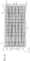
- Fig. 1A is a plan view of the solar cell module according to Example 1.
- Fig. 1B is a cross-sectional view taken along the line IB-IB in Fig. 1A , illustrating the solar cell module according to Example 1.
- the Z-axis is perpendicular to the principal surface of solar cell module 1, and the X-axis and Y-axis are orthogonal to each other and also are both orthogonal to the Z-axis (the thickness direction of the solar cells).
- the Z-axis, X-axis and Y-axis the same applies to the following drawings.
- solar cell module 1 includes solar cells 10, tab wiring members 20, light reflection member 30, front protective member 40, back protective member 50, bonding layer 60 and frame 70.
- Solar cell module 1 has a structure in which solar cells 10 are sealed between front protective member 40 and back protective member 50 by bonding layer 60.
- solar cell module 1 has an approximately rectangular shape, for example, in a planar view.
- solar cell module 1 has an approximately rectangular shape that is about 1600 mm in width and about 800 mm in length. Note that the shape of solar cell module 1 is not limited to a rectangular shape.
- Fig. 2A is an enlarged view of Region X surrounded by the broken line in Fig. 1A , and is a partially enlarged plan view of the solar cell module according to Example 1.
- Fig. 2B is a cross-sectional view taken along the line IIB-IIB in Fig. 2A , illustrating the solar cell module according to Example 1. Note that Fig. 2B is an enlarged cross-sectional view around light reflection member 30.
- Solar cells 10 are photoelectric conversion elements (photovoltaic elements), which convert light such as sunlight into electric power. As illustrated in Fig. 1A , solar cells 10 are arranged in a line-column pattern (matrix) in the same plane.
- solar cells 10 linearly arranged along one of a row direction and a column direction, two solar cells 10 adjacent to each other are connected by tab wiring members 20 to form a string (cell string). Multiple solar cells 10 are electrically connected by tab wiring members 20 to form a string. Solar cells 10 in one string 10S are connected in series by tab wiring members 20.
- each string 10S is formed by sequentially connecting two solar cells 10 adjacent to each other in the row direction (X-axis direction) with three tab wiring members 20. All solar cells 10 in a line arranged along the row direction are connected.
- Strings 10S are formed in multiple numbers. Strings 10S (strings) are arranged along the other one of the row direction and the column direction. In this embodiment, six strings 10S are formed. As illustrated in Fig. 1A , six strings 10S are arranged equally spaced apart along the column direction (Y-axis direction) or a second direction so as to be parallel to each other.
- each string 10S is connected to an interconnection wiring member (not illustrated) through tab wiring members 20.
- the last solar cell 10 in each string 10S is connected to an interconnection wiring member (not illustrated) through tab wiring members 20.
- more than one string 10S (six strings in Fig. 1A ) is connected in series or connected in parallel to form a cell array.
- two strings 10S adjacent to each other are connected in series to form one series connection body (twenty-four series-connected solar cells 10), and three series connection bodies are connected in parallel.
- solar cells 10 are arranged with a gap between solar cells 10 adjacent to each other in the row direction and column direction. As described later, light reflection member 30 is disposed in the gap.
- solar cell 10 has an approximately rectangular shape in a planar view.
- solar cell 10 has a 125 ⁇ 125 mm square shape with chamfered corners. That is, one string 10S is configured such that two solar cells 10 adjacent to each other have their one sides facing each other. Note that the shape of solar cell 10 is not limited to the approximately rectangular shape.
- Solar cell 10 has a semiconductor pin junction as a basic structure.
- solar cell 10 includes: an n-type single crystal silicon substrate, which is an n-type semiconductor substrate; an i-type amorphous silicon layer, an n-type amorphous silicon layer and an n-side surface electrode, which are sequentially formed on one principal surface side (front side) of the n-type single crystal silicon substrate; and an i-type amorphous silicon layer, a p-type amorphous silicon layer and a p-side surface electrode, which are sequentially formed on the other principal surface side (back side) of the n-type single crystal silicon substrate.
- the n-side surface electrode and the p-side surface electrode are transparent electrodes made of ITO (Indium Tin Oxide) or the like, for example. Note that, since solar cell module 1 in this embodiment is of a single-sided light receiving type, the p-side surface electrode does not have to be transparent but may be a reflective metal electrode, for example.
- front-side collector electrode 11 (n-side collector electrode), which is electrically connected to the n-side surface electrode in solar cell 10, and back-side collector electrode 12 (p-side collector electrode), which is electrically connected to the p-side surface electrode in solar cell 10, are formed.
- each of front-side collector electrode 11 and back-side collector electrode 12 includes: finger electrodes linearly formed so as to be orthogonal to the extending direction of tab wiring members 20; and bus bar electrodes connected to the finger electrodes and linearly formed along a direction orthogonal to the finger electrodes (the extending direction of tab wiring members 20).
- the number of the bus bar electrodes is the same as that of tab wiring members 20, for example, and is three in this embodiment.
- front-side collector electrode 11 and back-side collector electrode 12 have the same shape, but the invention is not limited thereto.
- Front-side collector electrode 11 and back-side collector electrode 12 are made of a low-resistance conductive material such as silver (Ag).
- front-side collector electrode 11 and back-side collector electrode 12 can be formed by screen printing conductive paste (silver paste or the like) in a predetermined pattern on the n-side surface electrode and the p-side surface electrode, the conductive paste having a conductive filler such as silver dispersed in binder resin.
- both of the front surface (n-side surface) and the back surface (p-side surface) serve as light-receiving surfaces.
- carriers are generated in a photoelectric conversion body in solar cell 10.
- the generated carriers diffuse into the n-side surface electrode and the p-side surface electrode as a photocurrent, and then are collected by front-side collector electrode 11 and back-side collector electrode 12 before flowing into tab wiring members 20.
- front-side collector electrode 11 and back-side collector electrode 12 By providing front-side collector electrode 11 and back-side collector electrode 12 as described above, the carriers generated in solar cell 10 can be efficiently taken out to an external circuit.
- tab wiring member 20 electrically connects two adjacent solar cells 10 to each other in string 10S.
- two adjacent solar cells 10 are connected by three tab wiring members 20 disposed approximately parallel to each other.
- Tab wiring members 20 are provided so as to extend along the arrangement direction of two solar cells 10 to be connected.
- Each of tab wiring members 20 is an elongated conductive wiring member, and is a ribbon-shaped metal foil, for example.
- Tab wiring member 20 can be fabricated, for example, by cutting a metal foil, such as a copper foil and a silver foil, with its entire surface covered with solder, silver or the like into rectangles each having a predetermined length.
- each of tab wiring members 20 has one end thereof disposed on the front surface of one of two adjacent solar cells 10, and the other end disposed on the back surface of the other one of two adjacent solar cells 10.
- Each of tab wiring members 20 electrically connects the n-side collector electrode (front-side collector electrode) in one solar cell 10 to the p-side collector electrode (back-side collector electrode) in the other solar cell 10, as for two adjacent solar cells 10.
- tab wiring member 20 is connected to the bus bar electrode of front-side collector electrode 11 in one solar cell 10 and the bus bar electrode of back-side collector electrode 12 in the other solar cell 10.
- Tab wiring member 20 and front-side collector electrode 11 (back-side collector electrode 12) are bonded by thermocompression bonding with a conductive adhesive, for example, sandwiched therebetween.
- tab wiring member 20 and front-side collector electrode 11 may be bonded not with the conductive adhesive but with a solder material.
- tab wiring member 20 may have unevenness provided on its surface.
- the unevenness provided on the surface of tab wiring member 20 scatters the light to be reflected on an interface between front protective member 40 and an air layer or an interface between front protective member 40 and bonding layer 60, thus enabling the light to be guided to solar cells 10.
- This enables the light reflected by the surface of tab wiring member 20 to effectively contribute to power generation. As a result, power generation efficiency of solar cell module 1 is improved.
- tab wiring member 20 As tab wiring member 20 described above, one having a silver deposited film formed on the surface of copper foil having unevenness as a surface shape can be used. Note that tab wiring member 20 may have a flat surface rather than such an uneven shape. Moreover, a light reflection member having an uneven surface may be additionally laminated on a tab wiring member having a flat surface.
- light reflection member 30 is provided in solar cell 10.
- Light reflection member 30 is at least partially positioned on a side of solar cell 10.
- light reflection member 30 is provided between two adjacent solar cells 10 (first solar cell 10A and second solar cell 10B) disposed with a gap therebetween.
- more than one light reflection member 30 is provided along a longitudinal direction of string 10S in a gap between two adjacent strings 10S.
- light reflection members 30 are provided in every gap between two solar cells 10.
- each of light reflection members 30 is a tape-shaped light reflection sheet extending in the longitudinal direction of string 10S, and has an elongated rectangular shape and a thin plate shape, as an example.
- Light reflection member 30 has a length of 100 mm to 130 mm and a width of 1 mm to 20 mm, for example.
- Each light reflection member 30 covers the gap between two adjacent solar cells 10. That is, the width of light reflection member 30 is the same as the distance of the gap between two adjacent solar cells 10. Note that the width of light reflection member 30 is not limited thereto but may be smaller than the distance of the gap between two adjacent solar cells 10, for example.
- Light made incident on light reflection member 30 is reflected.
- Light reflection member 30 in this embodiment diffuses and reflects the incident light and thus functions as a light diffusion reflection member. That is, light reflection member 30 is a light diffusion reflection sheet.
- light reflection member 30 includes: insulating member 31 made of an insulating material; and conductive light reflection film 32 formed on the surface of insulating member 31. That is, light reflection member 30 has a laminated structure of insulating member 31 and conductive light reflection film 32.
- Insulating member 31 is made of an insulating resin material such as polyethylene terephthalate (PET) or acrylic, for example.
- conductive light reflection film 32 is a metal reflective film made of metal such as aluminum or silver, for example. In this embodiment, conductive light reflection film 32 is an aluminum deposited film.
- unevenness 30a is formed on the surface of insulating member 31.
- Conductive light reflection film 32 made of a metal film is formed on the surface of unevenness 30a by vapor deposition or the like, for example. Therefore, conductive light reflection film 32 has uneven surface shape along with the uneven shape of unevenness 30a. The uneven shape of conductive light reflection film 32 enables light made incident on light reflection member 30 to be diffused and reflected in a predetermined direction.
- the height between the concave (valley) and convex (mountain) is 5 ⁇ m to 100 ⁇ m, and the interval (pitch) between adjacent convexes is 20 ⁇ m to 400 ⁇ m.
- the height between the concave and convex is 12 ⁇ m, and the interval (pitch) between adjacent convexes is 40 ⁇ m.
- light reflection member 30 is disposed such that the surface of conductive light reflection film 32 faces front protective member 40. That is, light reflection member 30 is disposed such that insulating member 31 is positioned on the back protective member 50 side and the surface (back surface) of conductive light reflection film 32 on the solar cell 10 side is positioned on the front protective member 40 side.
- the material of insulating member 31 may be any of a translucent or transparent material such as a transparent material and a non-transparent material such as a white material and a black material.
- light reflection member 30 is provided not on back protective member 50 or the like, but in a power generation ineffective region at the edge of solar cell 10.
- productivity is improved and power generation capacity of solar cell 10 can be efficiently utilized.
- the thickness d M of light reflection member 30 is larger than the thickness dc of solar cell 10 (d M > dc).
- the thickness d M of light reflection member 30 is the total thickness including the thickness of insulating member 31 and the thickness of conductive light reflection film 32.
- conductive light reflection film 32 of light reflection member 30 is positioned outside the surface of solar cell 10.
- light reflection member 30 is configured such that conductive light reflection film 32 is positioned outside front-side collector electrode 11 in a direction away from solar cell 10. Therefore, d M - dx > dc is established, where dx is the height of the unevenness of conductive light reflection film 32.
- the thickness dc of solar cell 10 is about 200 ⁇ m.
- the height of the unevenness of conductive light reflection film 32 is 5 ⁇ m to 100 ⁇ m.
- a value (d M - dx) obtained by subtracting the height of the unevenness of conductive light reflection film 32 from the thickness of light reflection member 30 may be set to 200 ⁇ m or more, e.g., 250 ⁇ m to 500 ⁇ m.
- the thickness d M of light reflection member 30 is preferably larger by 55 ⁇ m or more than a sum of the thickness dc of solar cell 10 and the height dx of the unevenness of conductive light reflection film 32.
- an added distance (d1+d2) that is a sum of a distance d1 between first solar cell 10A and conductive light reflection film 32 and a distance d2 between second solar cell 10B and conductive light reflection film 32 is preferably 110 ⁇ m or more.
- Light reflection member 30 thus configured is sealed by bonding layer 60. That is, light reflection member 30 is bonded and fixed by bonding layer 60.
- the shape of unevenness 30a in light reflection member 30 is a triangular groove shape along the longitudinal direction of light reflection member 30.
- the invention is not limited thereto, but the shape thereof may be a conical shape, a quadrangular pyramid shape, a polyangular pyramid shape, a combination thereof or the like, as long as the shape can scatter light.
- Front protective member 40 is a member configured to protect the front surface of solar cell module 1, and protects the inside (solar cells 10 and the like) of solar cell module 1 from the external environment such as weather and external impact. As illustrated in Fig. 1B , front protective member 40 is provided on the front side (n-side) of solar cell 10, and protects the front-side light receiving surface of solar cell 10.
- Front protective member 40 includes a transparent member that transmits light in a wavelength band used for photoelectric conversion in solar cell 10.
- Front protective member 40 is, for example, a glass substrate (transparent glass substrate) made of a transparent glass material or a resin substrate made of a film-shaped or plate-shaped transparent and water-impervious hard resin material.
- back protective member 50 (second protective member) is a member configured to protect the back surface of solar cell module 1, and protects the inside of solar cell module 1 from the external environment. As illustrated in Fig. 1B , back protective member 50 is provided on the back side (p-side) of solar cell 10.
- Back protective member 50 is a film-shaped or plate-shaped resin sheet made of a resin material such as polyethylene terephthalate (PET) and polyethylene naphthalate (PEN), for example.
- PET polyethylene terephthalate
- PEN polyethylene naphthalate
- back protective member 50 may be a non-transparent plate body or film.
- a non-transparent member such as a black member or a laminated film such as a resin film having metal foil such as aluminum foil therein.
- back protective member 50 is not limited to the non-transparent member but may be a transparent member such as a glass sheet or a glass substrate made of a glass material.
- Bonding layer 60 is provided between front protective member 40 and back protective member 50. Front protective member 40 and back protective member 50 are bonded and fixed to solar cells 10 by bonding layer 60.
- Bonding layer (filler material) 60 is disposed between front protective member 40 and back protective member 50.
- bonding layer 60 is provided to fill a space between front protective member 40 and back protective member 50.
- bonding layer 60 includes front-side bonding layer 61 and back-side bonding layer 62.
- Solar cells 10 are entirely covered with bonding layer 60 by performing lamination (laminate processing) in a state where the solar cells are sandwiched between sheet-like front-side bonding layer 61 and back-side bonding layer 62, for example.
- strings 10S are formed by connecting solar cells 10 with tab wiring members 20
- strings 10S are sandwiched between front-side bonding layer 61 and back-side bonding layer 62.
- front protective member 40 and back protective member 50 are further disposed thereabove and therebelow, and thermocompression bonding is performed in a vacuum at a temperature of 100°C or more, for example. This thermocompression bonding heats and melts front-side bonding layer 61 and back-side bonding layer 62 to form bonding layer 60 that seals solar cells 10.
- Front-side bonding layer 61 is a resin sheet made of a resin material such as ethylene-vinyl acetate (EVA), for example, and is disposed between solar cells 10 and front protective member 40.
- the front-side bonding layer is mainly provided so as to fill a space between solar cells 10 and front protective member 40 by laminate processing.
- front-side bonding layer 61 is a transparent resin sheet.
- front-side bonding layer 61 is a transparent resin sheet made of a hot-melt adhesive of EVA.
- Back-side bonding layer 62 is a resin sheet made of a resin material such as ethylene-vinyl acetate (EVA), for example, and is disposed between solar cells 10 and back protective member 50 .
- Back-side bonding layer 62 is mainly provided so as to fill a space between solar cells 10 and back protective member 50 by laminate processing.
- a black or white resin sheet is used as back-side bonding layer 62.
- back-side bonding layer 62 is a white resin sheet made of a hot-melt adhesive of EVA.
- Frame 70 is an outer frame that covers the peripheral edge of solar cell module 1.
- Frame 70 is an aluminum frame made of aluminum, for example. As illustrated in Fig. 1A , four frames 70 are used and attached to the four sides of solar cell module 1, respectively. Frames 70 are fixed to the respective sides of solar cell module 1 with an adhesive, for example.
- solar cell module 1 is provided with a terminal box to take out power generated by solar cells 10.
- the terminal box is fixed to back protective member 50, for example.
- the terminal box includes circuit components mounted on a circuit board.
- FIG. 3 is a partially enlarged cross-sectional view of the solar cell module according to the comparative example.
- light reflection member 30 is disposed in a gap between two adjacent solar cells 10, as in the case of solar cell module 1 according to this embodiment.
- solar cell module 1A of the comparative example is different from solar cell module 1 according to this embodiment in that the thickness of light reflection member 30 is smaller than that of solar cell 10. Therefore, in solar cell module 1A of the comparative example, a leak current may be generated between solar cells 10 through conductive light reflection film 32 of light reflection member 30.
- solar cell 10 is made of a semiconductor material, and thus the semiconductor material may be present in a side portion of solar cell 10. In this case, if the thickness of light reflection member 30 is smaller than that of solar cell 10, a leak current is generated between solar cells 10 through conductive light reflection film 32 of light reflection member 30.
- the thickness d M of light reflection member 30 is larger than the thickness dc of solar cell 10, and the surface of conductive light reflection film 32 on the solar cell 10 side is positioned outside the surface of solar cell 10 (on the front protective member 40 side).
- conductive light reflection film 32 of light reflection member 30 can be spaced from the surface of solar cell 10.
- the generation of the leak current can be effectively suppressed.
- reliability of solar cell module 1 is improved.
- light reflection member 30 is disposed such that the surface of conductive light reflection film 32 faces front protective member 40.
- light reflection member 30 may be disposed such that the surface of conductive light reflection film 32 faces back protective member 50. That is, light reflection member 30 may be disposed such that insulating member 31 is positioned on the front protective member 40 side and conductive light reflection film 32 is positioned on the back protective member 50 side.
- the thickness of light reflection member 30 is larger than the thickness dc of solar cell 10, and the surface of conductive light reflection film 32 on the solar cell 10 side is positioned outside the surface of solar cell 10 (on the back protective member 50 side).
- the generation of the leak current can be suppressed.
- the thickness d M of light reflection member 30 is larger by 55 ⁇ m or more than a sum of the thickness dc of solar cell 10 and the height dx of the unevenness of conductive light reflection film 32.
- adjacent solar cells 10 are required to be resistant to application of an impulse voltage of 800 V, for example.
- an insulating distance of 110 ⁇ m or more is ensured between adjacent solar cells 10. That is, the insulating distance of 110 ⁇ m or more can be ensured between adjacent solar cells 10 by setting the thickness d M of light reflection member 30 to be larger by 55 ⁇ m or more than the sum of the thickness dc of solar cell 10 and the height dx of the unevenness of conductive light reflection film 32. Accordingly, also for the application of the impulse voltage, the generation of the leak current due to breakdown can be effectively suppressed. As a result, the reliability of solar cell module 1 is further improved.
- the added distance (d1 + d2) that is the sum of the distance d1 between first solar cell 10A and conductive light reflection film 32 and the distance d2 between second solar cell 10B and conductive light reflection film 32 is 110 ⁇ m or more.
- the insulating distance of 110 ⁇ m or more is ensured between first solar cell 10A and second solar cell 10B.
- insulating member 31 may include a translucent member such as a transparent member.
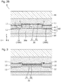
- FIGS. 5A and 5B are enlarged cross-sectional views around a light reflection member in the solar cell module according to Embodiment 2.
- light reflection member 30 is provided so as to extend beyond a gap between two adjacent solar cells 10 and overlap with the edge of the solar cell 10.
- light reflection member 30 is disposed over two adjacent solar cells 10 (first solar cell 10A and second solar cell 10B). To be more specific, light reflection member 30 is provided at the edge of first solar cell 10A such that one end of light reflection member 30 in the width direction overlaps with first solar cell 10A. Also, light reflection member 30 is provided at the edge of second solar cell 10B such that the end of light reflection member 30 in the width direction overlaps with second solar cell 10B.
- the thickness of light reflection member 30 is larger than that of solar cell 10.
- conductive light reflection film 32 of light reflection member 30 in the fall-off portion is positioned outside the surface of solar cell 10 (on the back protective member 50 side) . Also, there is a case where light reflection member 30 entirely falls off solar cell 10, resulting in a state as illustrated in Fig. 2B . However, even in such a case, conductive light reflection film 32 of light reflection member 30 is positioned outside the surface of solar cell 10.
- light reflection member 30 is disposed such that the surface of conductive light reflection film 32 faces front protective member 40.
- light reflection member 30 may be disposed such that the surface of conductive light reflection film 32 faces back protective member 50.
- the thickness of light reflection member 30 is set larger than that of solar cell 10, and the surface of conductive light reflection film 32 on the solar cell 10 side is positioned outside the surface of solar cell 10.
- an added distance (d1 + d2) that is a sum of a distance d1 between first solar cell 10A and conductive light reflection film 32 and a distance d2 between second solar cell 10B and conductive light reflection film 32 is 110 ⁇ m or more.
- first solar cell 10A and second solar cell 10B an insulating distance of 110 ⁇ m or more is ensured between first solar cell 10A and second solar cell 10B. Accordingly, also for the application of an impulse voltage of 800 V, the generation of the leak current due to breakdown can be surely suppressed.
- light reflection member 30 illustrated in Figs. 5A and 5B has conductive light reflection film 32 on the front protective member 40 side.
- the material of insulating member 31 may be any of a translucent material such as a transparent material and a non-transparent material such as a white material and a black material.
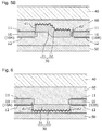
- light reflection member 30A illustrated in Fig. 6 has conductive light reflection film 32 on the back protective member 50 side.
- the material of insulating member 31 is preferably a translucent material such as a transparent material.
- FIG. 7 is an enlarged cross-sectional view around a light reflection member in the solar cell module according to Example 3.
- solar cell module 3 has a configuration in which insulating member 31 has a laminated structure of resin base material 31a and adhesive layer 31b, and conductive light reflection film 32 is formed on the surface of resin base material 31a opposite to the adhesive layer 31b side, in solar cell module 1 according to Example 1 described above.
- light reflection member 30A has a configuration including adhesive layer 31b provided beforehand.
- light reflection member 30A includes: resin base material 31a; conductive light reflection film 32 formed on one surface of resin base material 31a; and adhesive layer 31b provided on the other surface of resin base material 31a.
- Resin base material 31a is made of an insulating resin material such as PET or acrylic, for example.
- adhesive layer 31b is a resin adhesive made of an insulating resin material such as EVA.
- resin base material 31a is a PET sheet
- adhesive layer 31b is a heat-sensitive adhesive or a pressure-sensitive adhesive made of EVA.
- unevenness 30a is formed on the surface of resin base material 31a.
- conductive light reflection film 32 has an uneven surface.
- the thickness of light reflection member 30A is larger than the thickness of solar cell 10, and the surface of conductive light reflection film 32 on the solar cell 10 side is positioned outside the surface of solar cell 10 (on the front protective member 40 side).
- conductive light reflection film 32 of light reflection member 30A can be spaced from the surface of solar cell 10.
- generation of a leak current can be effectively suppressed.
- reliability of solar cell module 1 is improved.
- light reflection member 30A since light reflection member 30A has adhesive layer 31b, light reflection member 30A can be easily disposed at a predetermined position.
- light reflection member 30A is disposed such that the surface of conductive light reflection film 32 faces front protective member 40.
- light reflection member 30A may be disposed such that the surface of conductive light reflection film 32 faces back protective member 50.
- the thickness of light reflection member 30A is set larger than that of solar cell 10, and the surface of conductive light reflection film 32 on the solar cell 10 side is positioned outside the surface of solar cell 10 (on the back protective member 50 side). Thus, the generation of the leak current can be suppressed.
- the thickness d M of light reflection member 30A illustrated in Figs. 7 and 8 is larger by 55 ⁇ m or more than a sum of the thickness dc of solar cell 10 and the height dx of the unevenness of conductive light reflection film 32.
- an insulating distance of 110 ⁇ m or more can be ensured between adjacent solar cells 10. Accordingly, also for the application of an impulse voltage of 800 V, for example, the generation of the leak current due to breakdown can be effectively suppressed.
- an added distance (d1 + d2) that is a sum of a distance d1 between first solar cell 10A and conductive light reflection film 32 and a distance d2 between second solar cell 10B and conductive light reflection film 32 is 110 ⁇ m or more.
- an insulating distance of 110 ⁇ m or more is ensured between first solar cell 10A and second solar cell 10B. Accordingly, also for the application of the impulse voltage described above, the generation of the leak current due to breakdown can be surely suppressed.
- light reflection member 30A illustrated in Fig. 7 has conductive light reflection film 32 on the front protective member 40 side.
- the materials of resin base material 31a and adhesive layer 31b may be any of a translucent material such as a transparent material and a non-transparent material such as a white material and a black material.
- light reflection member 30A illustrated in Fig. 8 has conductive light reflection film 32 on the back protective member 50 side.
- the materials of resin base material 31a and adhesive layer 31b are preferably a translucent material such as a transparent material.
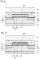
- FIG. 9 is an enlarged cross-sectional view around a light reflection member in the solar cell module according to Embodiment 4.
- solar cell module 4 has a configuration in which insulating member 31 has a laminated structure of resin base material 31a and adhesive layer 31b, and conductive light reflection film 32 is formed on the surface of resin base material 31a opposite to the adhesive layer 31b side, in solar cell module 2 according to Embodiment 2 described above.
- light reflection member 30A includes: resin base material 31a; conductive light reflection film 32 formed on one surface of resin base material 31a; and adhesive layer 31b provided on the other surface of resin base material 31a. Note that materials and structures of resin base material 31a and adhesive layer 31b are the same as those in Example 3.
- the thickness of light reflection member 30A is larger than the thickness of solar cell 10.
- light reflection member 30A since light reflection member 30A has adhesive layer 31b, light reflection member 30A can be easily disposed at the edge of solar cell 10.
- solar cells 10 can be attached at a predetermined position of light reflection member 30A before string 10S including solar cells 10 connected by tab wiring members 20 is subjected to laminate processing using front-side bonding layer 61 and back-side bonding layer 62. Therefore, light reflection member 30A can be accurately disposed.
- Fig. 11A is an enlarged cross-sectional view around a light reflection member in the solar cell module according to Embodiment 4 illustrated in Fig. 9 .
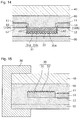
- Fig. 11B is an enlarged cross-sectional view around a light reflection member in a solar cell module according to Modified Example 1 of Embodiment 4 illustrated in Fig. 10 .
- thermocompression bonding occurs after strings 10S are formed by connecting solar cells 10 with tab wiring members 20. That is, strings 10S having light reflection member 30A disposed on solar cells 10 are sandwiched between front-side bonding layer 61 and back-side bonding layer 62 and between front protective member 40 and back protective member 50, and then thermocompression bonding is performed. The thermocompression bonding during the laminate processing in this event causes light reflection member 30A to be pressurized from front-side bonding layer 61 and back-side bonding layer 62.
- the pressing force during the laminate processing may cause light reflection member 30A to be curved so as to protrude toward the gap between two adjacent solar cells 10.
- light reflection member 30A is curved, light entering light reflection member 30A cannot be guided to a desired spot on solar cell 10. As a result, a desired effect of improving power generation efficiency by disposing light reflection member 30A cannot be achieved.
- the curvature in light reflection member 30A can be suppressed even if a pressure is applied onto light reflection member 30A during the laminate processing.
- the light entering light reflection member 30A can be reflected and guided to a desired spot on solar cell 10.
- the desired effect of improving the power generation efficiency by disposing light reflection member 30A can be achieved.
- Fig. 12A is a partially enlarged cross-sectional view of another aspect of the solar cell module according to Modified Example 1 of Embodiment 4 illustrated in Fig. 10 .
- Fig. 12B is a partially enlarged back view of the same solar cell module illustrated in Fig. 12A .
- the pressing force during the laminate processing can cause adhesive layer 31b of light reflection member 30A to run around solar cell 10 to the back surface (the surface opposite to the surface where light reflection member 30A is firstly provided) of solar cell 10.
- back-side collector electrode 12 provided on the back surface of solar cell 10 can be partially covered with adhesive layer 31b running around solar cell 10 to the back surface of solar cell 10.
- edges of finger electrodes in back-side collector electrode 12 are covered with adhesive layer 31b.
- the edges of back-side collector electrode 12 can be held by adhesive layer 31b.
- peeling-off of the edges of the finger electrodes in back-side collector electrode 12 can be suppressed.
- light reflection member 30A is disposed such that the surface of conductive light reflection film 32 faces front protective member 40.
- light reflection member 30A may be disposed such that the surface of conductive light reflection film 32 faces back protective member 50.
- the thickness of light reflection member 30A is set larger than that of solar cell 10, and the surface of conductive light reflection film 32 on the solar cell 10 side is positioned outside the surface of solar cell 10.
- an added distance (d1 + d2) that is a sum of a distance d1 between first solar cell 10A and conductive light reflection film 32 and a distance d2 between second solar cell 10B and conductive light reflection film 32 is 110 ⁇ m or more.
- light reflection member 30A illustrated in Figs. 9 and 10 has conductive light reflection film 32 on the front protective member 40 side.
- the materials of resin base material 31a and adhesive layer 31b may be any of a translucent material such as a transparent material and a non-transparent material such as a white material and a black material.
- light reflection member 30A illustrated in Figs. 13 and 14 has conductive light reflection film 32 on the back protective member 50 side.
- the materials of resin base material 31a and adhesive layer 31b are preferably a translucent material such as a transparent material.
- light reflection members 30 and 30A are disposed between two adjacent solar cells 10.
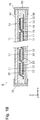
- light reflection members 30 and 30A may be disposed adjacent to the outermost solar cell 10 adjacent to frame 70, as illustrated in Fig. 15 .
- light reflection member 30 may be disposed upside down or may be disposed so as to overlap with the edge on the front or back surface of solar cell 10.
- light reflection members 30 and 30A are disposed in the gap between two adjacent strings 10S.
- the invention is not limited thereto.
- light reflection member 300 may be disposed in a gap between two adjacent solar cells 10 within string 10S.
- light reflection members 30 and 30A are provided for all solar cells 10. However, light reflection members 30 and 30A may be provided for only some 10. However, light reflection members 30 and 30A may be provided for only some of solar cells 10. That is, there may be solar cells where light reflection member 30 is not provided.
- light reflection members 30 and 30A are provided in every gap between solar cells 10 adjacent to each other along the longitudinal direction of string 10S in the gap between two adjacent strings 10S.
- the invention is not limited thereto.
- light reflection members 30 and 30A may be provided over solar cells 10 along the longitudinal direction of string 10S in the gap between two adjacent strings 10S.
- light reflection members 30 and 30A may be one elongated light reflection sheet across the entire string 10S.
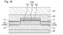
- conductive light reflection film 32 is formed on the top surface of light reflection members 30 and 30A.
- light reflection member 30B may have a configuration in which insulating member 33 (second insulating member) is further formed on conductive light reflection film 32 formed on insulating member 31 (first insulating member).
- insulating member 33 may be a transparent member made of a transparent resin material.
- the number of light reflection members 30 and 30A provided in the gap between two adjacent solar cells 10 may be two or more rather than one.
- the semiconductor substrate in solar cell 10 is the n-type semiconductor substrate.
- the semiconductor substrate may be a p-type semiconductor substrate.
- the solar cell module is of the single-sided light receiving type
- back protective member 50 serve as the light-receiving surfaces.
- the semiconductor material of the photoelectric converter in solar cell 10 is silicon.
- the invention is not limited thereto.
- gallium arsenide (GaAs), indium phosphide (InP) or the like may be used.
Landscapes
- Photovoltaic Devices (AREA)
Claims (4)
- Solarzellenmodul (2, 4) mit:einer ersten Solarzelle (10, 10A),einer zweiten Solarzelle (10, 10B), die mit einem Abstand von der ersten Solarzelle (10, 10A) in einer ersten Richtung angeordnet ist,wobei jede der ersten und zweiten Solarzelle (10, 10A, 10B) einen photoelektrischen Wandlerkörper mit einer vorderseitigen Kollektorelektrode (11) und einer rückseitigen Kollektorelektrode (12) aufweist, die jeweils aus leitender Paste gebildet sind,einem Lichtreflexionselement (30, 30A, 30B, 300), das zwischen der ersten Solarzelle (10, 10A) und der zweiten Solarzelle (10, 10B) in der ersten Richtung rechtwinklig zu einer Dickenrichtung der ersten Solarzelle (10, 10A) vorgesehen ist,einem vorderen Schutzelement (40) und einem hinteren Schutzelement (50),einer Vorderseiten-Verbindungsschicht (61) und einer Rückseiten-Verbindungsschicht (62), wobei die erste und die zweite Solarzelle (10, 10A, 10B) und das Lichtreflexionselement (30, 30A, 30B, 3000) zwischen der Vorderseiten-Verbindungsschicht (61) und der Rückseiten-Verbindungsschicht (62) zwischen dem vorderen Schutzelement (40) und dem hinteren Schutzelement (50) sandwichartig angeordnet sind, wobeidas Lichtreflexionselement (30, 30A, 30B, 300) ein Isolierelement (31) und einen leitfähigen Lichtreflexionsfilm (32) auf dem Isolierelement (31) in der Dickenrichtung aufweist, wobei das Lichtreflexionselement (30, 30A, 30B, 300) die erste Solarzelle (10A) und die zweite Solarzelle (10B) nicht elektrisch verbindet,eine Dicke des Lichtreflexionselements (30, 30A, 30B, 300) größer ist als eine Dicke der ersten Solarzelle (10, 10A) in der Dickenrichtung,der leitende Lichtreflexionsfilm (32) außerhalb der ersten Solarzelle (10, 10A) in der Dickenrichtung positioniert ist, wobei ein Ende des Lichtreflexionselements (30, 30A, 30B, 300) mit einer Kante einer Vorder- oder Rückfläche der ersten Solarzelle (10, 10A) derart in der Dickenrichtung gesehen überlappt, dass das eine Ende des Lichtreflexionselements (30, 30A, 30B, 300) in direktem Kontakt mit der Kante der Vorder- oder Rückfläche der ersten Solarzelle (10, 10A) in der Dickenrichtung steht, undwobei das Isolierelement (31) eine Mehrschichtstruktur mit einem Harzgrundmaterial (31a) und einer Klebeschicht (31b) aufweist, undder leitende Lichtreflexionsfilm (32) auf dem Harzgrundmaterial (31a) auf der Klebeschicht (31b) ausgebildet ist,wobei eine Dicke der Klebeschicht (31b) größer als die Dicke der ersten Solarzelle (10, 10A) ist.
- Solarzellenmodul (2, 4) nach Anspruch 1, wobei
das Lichtreflexionselement (30, 30A, 30B, 300) Brücken zwischen der ersten Solarzelle (10, 10A) und der zweiten Solarzelle (10, 10B) bildet. - Solarzellenmodul (2, 4) nach Anspruch 1 oder 2, wobei die Kollektorelektroden (11, 12) auf beiden Oberflächen der ersten Solarzelle (10, 10A) vorgesehen sind, wobei die beiden Oberflächen eine erste Oberfläche und eine zweite Oberfläche umfassen, die auf einer gegenüberliegenden Seite der ersten Solarzelle (10, 10A) vorgesehen ist, wobei die erste Oberfläche näher an dem leitfähigen Lichtreflexionsfilm (32) liegt als die zweite Oberfläche, und
die Klebeschicht (31b) um die erste Solarzelle (10, 10A) von der ersten Oberfläche zur zweiten Oberfläche verläuft und einen Teil der auf der zweiten Oberfläche vorgesehenen Kollektorelektrode bedeckt. - Solarzellenmodul (2, 4) nach Anspruch 1 oder 2, wobei eine Oberfläche des Isolierelements (31a), die dem leitenden Lichtreflexionsfilm (32) zugewandt ist, eine ungleichmäßige Oberflächenform aufweist,
eine Oberfläche des leitfähigen Lichtreflexionsfilms (32) zusammen mit der unebenen Oberfläche des Isolierelements (31) eine unebene Oberflächenform aufweist, und
die Dicke des Lichtreflexionselements (30, 30A, 30B, 300) um 55 µm oder mehr als die Summe der Dicke der ersten Solarzelle (10, 10A) und einer Höhe der unebenen Oberflächenform des leitfähigen Lichtreflexionsfilms (32) größer ist.
Applications Claiming Priority (2)
| Application Number | Priority Date | Filing Date | Title |
|---|---|---|---|
| JP2015050913 | 2015-03-13 | ||
| JP2015171577A JP6709977B2 (ja) | 2015-03-13 | 2015-08-31 | 太陽電池モジュール |
Publications (2)
| Publication Number | Publication Date |
|---|---|
| EP3067937A1 EP3067937A1 (de) | 2016-09-14 |
| EP3067937B1 true EP3067937B1 (de) | 2021-01-06 |
Family
ID=55527396
Family Applications (1)
| Application Number | Title | Priority Date | Filing Date |
|---|---|---|---|
| EP16159847.9A Not-in-force EP3067937B1 (de) | 2015-03-13 | 2016-03-11 | Solarzellenmodul |
Country Status (2)
| Country | Link |
|---|---|
| US (1) | US20160268466A1 (de) |
| EP (1) | EP3067937B1 (de) |
Families Citing this family (10)
| Publication number | Priority date | Publication date | Assignee | Title |
|---|---|---|---|---|
| WO2017154384A1 (ja) * | 2016-03-10 | 2017-09-14 | 株式会社カネカ | 太陽電池モジュール |
| JP1559309S (de) * | 2016-03-25 | 2016-09-26 | ||
| JP1561706S (de) * | 2016-03-25 | 2016-10-31 | ||
| USD828292S1 (en) * | 2016-06-27 | 2018-09-11 | Panasonic Intellectual Property Management Co., Ltd. | Solar battery module |
| CN109819682B (zh) | 2016-09-28 | 2022-09-02 | 松下知识产权经营株式会社 | 太阳能电池组件和太阳能电池组件的制造方法 |
| IT201600118568A1 (it) * | 2016-11-23 | 2018-05-23 | Martino Falsini | Modulo fotovoltaico |
| WO2018116899A1 (ja) * | 2016-12-22 | 2018-06-28 | パナソニックIpマネジメント株式会社 | 太陽電池モジュール |
| KR101934055B1 (ko) * | 2017-01-06 | 2019-04-05 | 엘지전자 주식회사 | 태양전지 패널 |
| CN111630666B (zh) * | 2018-01-24 | 2023-11-07 | 株式会社钟化 | 用于太阳能电池单元的连接部件组、以及使用该连接部件组的太阳能电池串和太阳能电池模块 |
| CN114709286B (zh) * | 2022-03-31 | 2023-03-24 | 盐城百佳年代薄膜科技有限公司 | 实现光伏电池片间隙透光收集的光伏组件 |
Citations (3)
| Publication number | Priority date | Publication date | Assignee | Title |
|---|---|---|---|---|
| US20090178704A1 (en) * | 2007-02-06 | 2009-07-16 | Kalejs Juris P | Solar electric module with redirection of incident light |
| US20120118352A1 (en) * | 2010-11-12 | 2012-05-17 | Semiconductor Energy Laboratory Co., Ltd. | Photoelectric conversion module and photoelectric conversion device |
| WO2012114918A1 (ja) * | 2011-02-24 | 2012-08-30 | 三洋電機株式会社 | 太陽電池モジュール及びその製造方法 |
Family Cites Families (10)
| Publication number | Priority date | Publication date | Assignee | Title |
|---|---|---|---|---|
| US5288337A (en) * | 1992-06-25 | 1994-02-22 | Siemens Solar Industries, L.P. | Photovoltaic module with specular reflector |
| JP4404753B2 (ja) * | 2004-11-24 | 2010-01-27 | 三洋電機株式会社 | 太陽電池モジュール |
| EP2109894A2 (de) * | 2007-01-31 | 2009-10-21 | Renewable Energy Corporation ASA | Verbindungsreflektorband für solarzellenmodule |
| JP5152858B2 (ja) * | 2008-08-22 | 2013-02-27 | シャープ株式会社 | 太陽電池モジュールおよびその製造方法 |
| JP2013098496A (ja) | 2011-11-04 | 2013-05-20 | Mitsubishi Electric Corp | 太陽電池モジュールおよびその製造方法 |
| CN102664210B (zh) * | 2012-05-14 | 2015-05-06 | 友达光电股份有限公司 | 太阳能模块与其制造方法 |
| KR101890324B1 (ko) * | 2012-06-22 | 2018-09-28 | 엘지전자 주식회사 | 태양 전지 모듈 및 이에 적용되는 리본 결합체 |
| JP6280692B2 (ja) * | 2013-03-21 | 2018-02-14 | デクセリアルズ株式会社 | 太陽電池モジュール、及び結晶系太陽電池モジュールの製造方法 |
| JP2014207305A (ja) * | 2013-04-12 | 2014-10-30 | 三洋電機株式会社 | 太陽電池モジュール |
| KR102257808B1 (ko) * | 2014-01-20 | 2021-05-28 | 엘지전자 주식회사 | 태양 전지 모듈 |
-
2016
- 2016-03-10 US US15/065,858 patent/US20160268466A1/en not_active Abandoned
- 2016-03-11 EP EP16159847.9A patent/EP3067937B1/de not_active Not-in-force
Patent Citations (3)
| Publication number | Priority date | Publication date | Assignee | Title |
|---|---|---|---|---|
| US20090178704A1 (en) * | 2007-02-06 | 2009-07-16 | Kalejs Juris P | Solar electric module with redirection of incident light |
| US20120118352A1 (en) * | 2010-11-12 | 2012-05-17 | Semiconductor Energy Laboratory Co., Ltd. | Photoelectric conversion module and photoelectric conversion device |
| WO2012114918A1 (ja) * | 2011-02-24 | 2012-08-30 | 三洋電機株式会社 | 太陽電池モジュール及びその製造方法 |
Also Published As
| Publication number | Publication date |
|---|---|
| EP3067937A1 (de) | 2016-09-14 |
| US20160268466A1 (en) | 2016-09-15 |
Similar Documents
| Publication | Publication Date | Title |
|---|---|---|
| EP3067937B1 (de) | Solarzellenmodul | |
| EP3067939B1 (de) | Solarzellenmodul | |
| US10879410B2 (en) | Solar cell module | |
| JP6709977B2 (ja) | 太陽電池モジュール | |
| JP6611062B2 (ja) | 太陽電池モジュール | |
| US10840402B2 (en) | Solar cell module | |
| US10629763B2 (en) | Solar cell module | |
| JP6883750B2 (ja) | 太陽電池モジュール | |
| JP2017050514A (ja) | 太陽電池モジュール | |
| JP2018056454A (ja) | 太陽電池モジュール及び太陽電池モジュールの製造方法 | |
| JP6731660B2 (ja) | 太陽電池モジュール | |
| JP2017063140A (ja) | 太陽電池モジュール |
Legal Events
| Date | Code | Title | Description |
|---|---|---|---|
| PUAI | Public reference made under article 153(3) epc to a published international application that has entered the european phase |
Free format text: ORIGINAL CODE: 0009012 |
|
| AK | Designated contracting states |
Kind code of ref document: A1 Designated state(s): AL AT BE BG CH CY CZ DE DK EE ES FI FR GB GR HR HU IE IS IT LI LT LU LV MC MK MT NL NO PL PT RO RS SE SI SK SM TR |
|
| AX | Request for extension of the european patent |
Extension state: BA ME |
|
| STAA | Information on the status of an ep patent application or granted ep patent |
Free format text: STATUS: REQUEST FOR EXAMINATION WAS MADE |
|
| 17P | Request for examination filed |
Effective date: 20170314 |
|
| RBV | Designated contracting states (corrected) |
Designated state(s): AL AT BE BG CH CY CZ DE DK EE ES FI FR GB GR HR HU IE IS IT LI LT LU LV MC MK MT NL NO PL PT RO RS SE SI SK SM TR |
|
| STAA | Information on the status of an ep patent application or granted ep patent |
Free format text: STATUS: EXAMINATION IS IN PROGRESS |
|
| 17Q | First examination report despatched |
Effective date: 20171212 |
|
| GRAP | Despatch of communication of intention to grant a patent |
Free format text: ORIGINAL CODE: EPIDOSNIGR1 |
|
| STAA | Information on the status of an ep patent application or granted ep patent |
Free format text: STATUS: GRANT OF PATENT IS INTENDED |
|
| INTG | Intention to grant announced |
Effective date: 20201001 |
|
| GRAS | Grant fee paid |
Free format text: ORIGINAL CODE: EPIDOSNIGR3 |
|
| GRAA | (expected) grant |
Free format text: ORIGINAL CODE: 0009210 |
|
| STAA | Information on the status of an ep patent application or granted ep patent |
Free format text: STATUS: THE PATENT HAS BEEN GRANTED |
|
| AK | Designated contracting states |
Kind code of ref document: B1 Designated state(s): AL AT BE BG CH CY CZ DE DK EE ES FI FR GB GR HR HU IE IS IT LI LT LU LV MC MK MT NL NO PL PT RO RS SE SI SK SM TR |
|
| REG | Reference to a national code |
Ref country code: GB Ref legal event code: FG4D |
|
| REG | Reference to a national code |
Ref country code: AT Ref legal event code: REF Ref document number: 1353309 Country of ref document: AT Kind code of ref document: T Effective date: 20210115 Ref country code: CH Ref legal event code: EP |
|
| REG | Reference to a national code |
Ref country code: DE Ref legal event code: R096 Ref document number: 602016050883 Country of ref document: DE |
|
| REG | Reference to a national code |
Ref country code: IE Ref legal event code: FG4D |
|
| REG | Reference to a national code |
Ref country code: NL Ref legal event code: MP Effective date: 20210106 |
|
| REG | Reference to a national code |
Ref country code: AT Ref legal event code: MK05 Ref document number: 1353309 Country of ref document: AT Kind code of ref document: T Effective date: 20210106 |
|
| REG | Reference to a national code |
Ref country code: LT Ref legal event code: MG9D |
|
| PG25 | Lapsed in a contracting state [announced via postgrant information from national office to epo] |
Ref country code: HR Free format text: LAPSE BECAUSE OF FAILURE TO SUBMIT A TRANSLATION OF THE DESCRIPTION OR TO PAY THE FEE WITHIN THE PRESCRIBED TIME-LIMIT Effective date: 20210106 Ref country code: FI Free format text: LAPSE BECAUSE OF FAILURE TO SUBMIT A TRANSLATION OF THE DESCRIPTION OR TO PAY THE FEE WITHIN THE PRESCRIBED TIME-LIMIT Effective date: 20210106 Ref country code: GR Free format text: LAPSE BECAUSE OF FAILURE TO SUBMIT A TRANSLATION OF THE DESCRIPTION OR TO PAY THE FEE WITHIN THE PRESCRIBED TIME-LIMIT Effective date: 20210407 Ref country code: LT Free format text: LAPSE BECAUSE OF FAILURE TO SUBMIT A TRANSLATION OF THE DESCRIPTION OR TO PAY THE FEE WITHIN THE PRESCRIBED TIME-LIMIT Effective date: 20210106 Ref country code: NL Free format text: LAPSE BECAUSE OF FAILURE TO SUBMIT A TRANSLATION OF THE DESCRIPTION OR TO PAY THE FEE WITHIN THE PRESCRIBED TIME-LIMIT Effective date: 20210106 Ref country code: BG Free format text: LAPSE BECAUSE OF FAILURE TO SUBMIT A TRANSLATION OF THE DESCRIPTION OR TO PAY THE FEE WITHIN THE PRESCRIBED TIME-LIMIT Effective date: 20210406 Ref country code: PT Free format text: LAPSE BECAUSE OF FAILURE TO SUBMIT A TRANSLATION OF THE DESCRIPTION OR TO PAY THE FEE WITHIN THE PRESCRIBED TIME-LIMIT Effective date: 20210506 Ref country code: NO Free format text: LAPSE BECAUSE OF FAILURE TO SUBMIT A TRANSLATION OF THE DESCRIPTION OR TO PAY THE FEE WITHIN THE PRESCRIBED TIME-LIMIT Effective date: 20210406 |
|
| PG25 | Lapsed in a contracting state [announced via postgrant information from national office to epo] |
Ref country code: SE Free format text: LAPSE BECAUSE OF FAILURE TO SUBMIT A TRANSLATION OF THE DESCRIPTION OR TO PAY THE FEE WITHIN THE PRESCRIBED TIME-LIMIT Effective date: 20210106 Ref country code: RS Free format text: LAPSE BECAUSE OF FAILURE TO SUBMIT A TRANSLATION OF THE DESCRIPTION OR TO PAY THE FEE WITHIN THE PRESCRIBED TIME-LIMIT Effective date: 20210106 Ref country code: LV Free format text: LAPSE BECAUSE OF FAILURE TO SUBMIT A TRANSLATION OF THE DESCRIPTION OR TO PAY THE FEE WITHIN THE PRESCRIBED TIME-LIMIT Effective date: 20210106 Ref country code: PL Free format text: LAPSE BECAUSE OF FAILURE TO SUBMIT A TRANSLATION OF THE DESCRIPTION OR TO PAY THE FEE WITHIN THE PRESCRIBED TIME-LIMIT Effective date: 20210106 Ref country code: AT Free format text: LAPSE BECAUSE OF FAILURE TO SUBMIT A TRANSLATION OF THE DESCRIPTION OR TO PAY THE FEE WITHIN THE PRESCRIBED TIME-LIMIT Effective date: 20210106 |
|
| PG25 | Lapsed in a contracting state [announced via postgrant information from national office to epo] |
Ref country code: IS Free format text: LAPSE BECAUSE OF FAILURE TO SUBMIT A TRANSLATION OF THE DESCRIPTION OR TO PAY THE FEE WITHIN THE PRESCRIBED TIME-LIMIT Effective date: 20210506 |
|
| REG | Reference to a national code |
Ref country code: DE Ref legal event code: R097 Ref document number: 602016050883 Country of ref document: DE |
|
| PG25 | Lapsed in a contracting state [announced via postgrant information from national office to epo] |
Ref country code: CZ Free format text: LAPSE BECAUSE OF FAILURE TO SUBMIT A TRANSLATION OF THE DESCRIPTION OR TO PAY THE FEE WITHIN THE PRESCRIBED TIME-LIMIT Effective date: 20210106 Ref country code: EE Free format text: LAPSE BECAUSE OF FAILURE TO SUBMIT A TRANSLATION OF THE DESCRIPTION OR TO PAY THE FEE WITHIN THE PRESCRIBED TIME-LIMIT Effective date: 20210106 Ref country code: MC Free format text: LAPSE BECAUSE OF FAILURE TO SUBMIT A TRANSLATION OF THE DESCRIPTION OR TO PAY THE FEE WITHIN THE PRESCRIBED TIME-LIMIT Effective date: 20210106 Ref country code: SM Free format text: LAPSE BECAUSE OF FAILURE TO SUBMIT A TRANSLATION OF THE DESCRIPTION OR TO PAY THE FEE WITHIN THE PRESCRIBED TIME-LIMIT Effective date: 20210106 |
|
| REG | Reference to a national code |
Ref country code: CH Ref legal event code: PL |
|
| PLBE | No opposition filed within time limit |
Free format text: ORIGINAL CODE: 0009261 |
|
| STAA | Information on the status of an ep patent application or granted ep patent |
Free format text: STATUS: NO OPPOSITION FILED WITHIN TIME LIMIT |
|
| PG25 | Lapsed in a contracting state [announced via postgrant information from national office to epo] |
Ref country code: SK Free format text: LAPSE BECAUSE OF FAILURE TO SUBMIT A TRANSLATION OF THE DESCRIPTION OR TO PAY THE FEE WITHIN THE PRESCRIBED TIME-LIMIT Effective date: 20210106 Ref country code: RO Free format text: LAPSE BECAUSE OF FAILURE TO SUBMIT A TRANSLATION OF THE DESCRIPTION OR TO PAY THE FEE WITHIN THE PRESCRIBED TIME-LIMIT Effective date: 20210106 Ref country code: ES Free format text: LAPSE BECAUSE OF FAILURE TO SUBMIT A TRANSLATION OF THE DESCRIPTION OR TO PAY THE FEE WITHIN THE PRESCRIBED TIME-LIMIT Effective date: 20210106 Ref country code: DK Free format text: LAPSE BECAUSE OF FAILURE TO SUBMIT A TRANSLATION OF THE DESCRIPTION OR TO PAY THE FEE WITHIN THE PRESCRIBED TIME-LIMIT Effective date: 20210106 |
|
| 26N | No opposition filed |
Effective date: 20211007 |
|
| REG | Reference to a national code |
Ref country code: BE Ref legal event code: MM Effective date: 20210331 |
|
| GBPC | Gb: european patent ceased through non-payment of renewal fee |
Effective date: 20210406 |
|
| PG25 | Lapsed in a contracting state [announced via postgrant information from national office to epo] |
Ref country code: GB Free format text: LAPSE BECAUSE OF NON-PAYMENT OF DUE FEES Effective date: 20210406 Ref country code: FR Free format text: LAPSE BECAUSE OF NON-PAYMENT OF DUE FEES Effective date: 20210331 Ref country code: IE Free format text: LAPSE BECAUSE OF NON-PAYMENT OF DUE FEES Effective date: 20210311 Ref country code: AL Free format text: LAPSE BECAUSE OF FAILURE TO SUBMIT A TRANSLATION OF THE DESCRIPTION OR TO PAY THE FEE WITHIN THE PRESCRIBED TIME-LIMIT Effective date: 20210106 Ref country code: CH Free format text: LAPSE BECAUSE OF NON-PAYMENT OF DUE FEES Effective date: 20210331 Ref country code: LU Free format text: LAPSE BECAUSE OF NON-PAYMENT OF DUE FEES Effective date: 20210311 Ref country code: LI Free format text: LAPSE BECAUSE OF NON-PAYMENT OF DUE FEES Effective date: 20210331 |
|
| PG25 | Lapsed in a contracting state [announced via postgrant information from national office to epo] |
Ref country code: SI Free format text: LAPSE BECAUSE OF FAILURE TO SUBMIT A TRANSLATION OF THE DESCRIPTION OR TO PAY THE FEE WITHIN THE PRESCRIBED TIME-LIMIT Effective date: 20210106 |
|
| PG25 | Lapsed in a contracting state [announced via postgrant information from national office to epo] |
Ref country code: IT Free format text: LAPSE BECAUSE OF FAILURE TO SUBMIT A TRANSLATION OF THE DESCRIPTION OR TO PAY THE FEE WITHIN THE PRESCRIBED TIME-LIMIT Effective date: 20210106 |
|
| PG25 | Lapsed in a contracting state [announced via postgrant information from national office to epo] |
Ref country code: IS Free format text: LAPSE BECAUSE OF FAILURE TO SUBMIT A TRANSLATION OF THE DESCRIPTION OR TO PAY THE FEE WITHIN THE PRESCRIBED TIME-LIMIT Effective date: 20210506 |
|
| PG25 | Lapsed in a contracting state [announced via postgrant information from national office to epo] |
Ref country code: BE Free format text: LAPSE BECAUSE OF NON-PAYMENT OF DUE FEES Effective date: 20210331 |
|
| PG25 | Lapsed in a contracting state [announced via postgrant information from national office to epo] |
Ref country code: HU Free format text: LAPSE BECAUSE OF FAILURE TO SUBMIT A TRANSLATION OF THE DESCRIPTION OR TO PAY THE FEE WITHIN THE PRESCRIBED TIME-LIMIT; INVALID AB INITIO Effective date: 20160311 |
|
| PGFP | Annual fee paid to national office [announced via postgrant information from national office to epo] |
Ref country code: DE Payment date: 20230321 Year of fee payment: 8 |
|
| PG25 | Lapsed in a contracting state [announced via postgrant information from national office to epo] |
Ref country code: CY Free format text: LAPSE BECAUSE OF FAILURE TO SUBMIT A TRANSLATION OF THE DESCRIPTION OR TO PAY THE FEE WITHIN THE PRESCRIBED TIME-LIMIT Effective date: 20210106 |
|
| PG25 | Lapsed in a contracting state [announced via postgrant information from national office to epo] |
Ref country code: MK Free format text: LAPSE BECAUSE OF FAILURE TO SUBMIT A TRANSLATION OF THE DESCRIPTION OR TO PAY THE FEE WITHIN THE PRESCRIBED TIME-LIMIT Effective date: 20210106 |
|
| PG25 | Lapsed in a contracting state [announced via postgrant information from national office to epo] |
Ref country code: MT Free format text: LAPSE BECAUSE OF FAILURE TO SUBMIT A TRANSLATION OF THE DESCRIPTION OR TO PAY THE FEE WITHIN THE PRESCRIBED TIME-LIMIT Effective date: 20210106 |
|
| REG | Reference to a national code |
Ref country code: DE Ref legal event code: R119 Ref document number: 602016050883 Country of ref document: DE |
|
| PG25 | Lapsed in a contracting state [announced via postgrant information from national office to epo] |
Ref country code: DE Free format text: LAPSE BECAUSE OF NON-PAYMENT OF DUE FEES Effective date: 20241001 |
|
| PG25 | Lapsed in a contracting state [announced via postgrant information from national office to epo] |
Ref country code: DE Free format text: LAPSE BECAUSE OF NON-PAYMENT OF DUE FEES Effective date: 20241001 |
|
| PG25 | Lapsed in a contracting state [announced via postgrant information from national office to epo] |
Ref country code: TR Free format text: LAPSE BECAUSE OF FAILURE TO SUBMIT A TRANSLATION OF THE DESCRIPTION OR TO PAY THE FEE WITHIN THE PRESCRIBED TIME-LIMIT Effective date: 20210106 |