EP3068029A1 - Umrichtersystem - Google Patents
Umrichtersystem Download PDFInfo
- Publication number
- EP3068029A1 EP3068029A1 EP16158904.9A EP16158904A EP3068029A1 EP 3068029 A1 EP3068029 A1 EP 3068029A1 EP 16158904 A EP16158904 A EP 16158904A EP 3068029 A1 EP3068029 A1 EP 3068029A1
- Authority
- EP
- European Patent Office
- Prior art keywords
- switching elements
- voltage
- inverter
- controller
- phase
- Prior art date
- Legal status (The legal status is an assumption and is not a legal conclusion. Google has not performed a legal analysis and makes no representation as to the accuracy of the status listed.)
- Withdrawn
Links
- 239000003990 capacitor Substances 0.000 claims abstract description 31
- 230000004044 response Effects 0.000 claims description 6
- 230000007935 neutral effect Effects 0.000 claims description 2
- 238000000034 method Methods 0.000 description 7
- 230000010363 phase shift Effects 0.000 description 6
- 238000010586 diagram Methods 0.000 description 4
- 230000000295 complement effect Effects 0.000 description 2
- 230000007423 decrease Effects 0.000 description 2
- 230000000694 effects Effects 0.000 description 2
- 230000006698 induction Effects 0.000 description 2
- 238000004519 manufacturing process Methods 0.000 description 2
- 239000000203 mixture Substances 0.000 description 2
- 238000012986 modification Methods 0.000 description 2
- 230000004048 modification Effects 0.000 description 2
- 230000001360 synchronised effect Effects 0.000 description 2
- 230000009466 transformation Effects 0.000 description 2
- 230000004075 alteration Effects 0.000 description 1
- 230000008859 change Effects 0.000 description 1
- 238000012423 maintenance Methods 0.000 description 1
- 230000008439 repair process Effects 0.000 description 1
- 238000000844 transformation Methods 0.000 description 1
Images


Classifications
-
- H—ELECTRICITY
- H02—GENERATION; CONVERSION OR DISTRIBUTION OF ELECTRIC POWER
- H02M—APPARATUS FOR CONVERSION BETWEEN AC AND AC, BETWEEN AC AND DC, OR BETWEEN DC AND DC, AND FOR USE WITH MAINS OR SIMILAR POWER SUPPLY SYSTEMS; CONVERSION OF DC OR AC INPUT POWER INTO SURGE OUTPUT POWER; CONTROL OR REGULATION THEREOF
- H02M5/00—Conversion of AC power input into AC power output, e.g. for change of voltage, for change of frequency, for change of number of phases
- H02M5/40—Conversion of AC power input into AC power output, e.g. for change of voltage, for change of frequency, for change of number of phases with intermediate conversion into DC
- H02M5/42—Conversion of AC power input into AC power output, e.g. for change of voltage, for change of frequency, for change of number of phases with intermediate conversion into DC by static converters
- H02M5/44—Conversion of AC power input into AC power output, e.g. for change of voltage, for change of frequency, for change of number of phases with intermediate conversion into DC by static converters using discharge tubes or semiconductor devices to convert the intermediate DC into AC
-
- H—ELECTRICITY
- H02—GENERATION; CONVERSION OR DISTRIBUTION OF ELECTRIC POWER
- H02M—APPARATUS FOR CONVERSION BETWEEN AC AND AC, BETWEEN AC AND DC, OR BETWEEN DC AND DC, AND FOR USE WITH MAINS OR SIMILAR POWER SUPPLY SYSTEMS; CONVERSION OF DC OR AC INPUT POWER INTO SURGE OUTPUT POWER; CONTROL OR REGULATION THEREOF
- H02M1/00—Details of apparatus for conversion
- H02M1/32—Means for protecting converters other than automatic disconnection
-
- H—ELECTRICITY
- H02—GENERATION; CONVERSION OR DISTRIBUTION OF ELECTRIC POWER
- H02H—EMERGENCY PROTECTIVE CIRCUIT ARRANGEMENTS
- H02H7/00—Emergency protective circuit arrangements specially adapted for specific types of electric machines or apparatus or for sectionalised protection of cable or line systems, and effecting automatic switching in the event of an undesired change from normal working conditions
- H02H7/10—Emergency protective circuit arrangements specially adapted for specific types of electric machines or apparatus or for sectionalised protection of cable or line systems, and effecting automatic switching in the event of an undesired change from normal working conditions for converters; for rectifiers
- H02H7/12—Emergency protective circuit arrangements specially adapted for specific types of electric machines or apparatus or for sectionalised protection of cable or line systems, and effecting automatic switching in the event of an undesired change from normal working conditions for converters; for rectifiers for static converters or rectifiers
- H02H7/122—Emergency protective circuit arrangements specially adapted for specific types of electric machines or apparatus or for sectionalised protection of cable or line systems, and effecting automatic switching in the event of an undesired change from normal working conditions for converters; for rectifiers for static converters or rectifiers for inverters, i.e. DC/AC converters
-
- H—ELECTRICITY
- H02—GENERATION; CONVERSION OR DISTRIBUTION OF ELECTRIC POWER
- H02M—APPARATUS FOR CONVERSION BETWEEN AC AND AC, BETWEEN AC AND DC, OR BETWEEN DC AND DC, AND FOR USE WITH MAINS OR SIMILAR POWER SUPPLY SYSTEMS; CONVERSION OF DC OR AC INPUT POWER INTO SURGE OUTPUT POWER; CONTROL OR REGULATION THEREOF
- H02M7/00—Conversion of AC power input into DC power output; Conversion of DC power input into AC power output
- H02M7/42—Conversion of DC power input into AC power output without possibility of reversal
- H02M7/44—Conversion of DC power input into AC power output without possibility of reversal by static converters
- H02M7/48—Conversion of DC power input into AC power output without possibility of reversal by static converters using discharge tubes with control electrode or semiconductor devices with control electrode
- H02M7/483—Converters with outputs that each can have more than two voltages levels
- H02M7/4835—Converters with outputs that each can have more than two voltages levels comprising two or more cells, each including a switchable capacitor, the capacitors having a nominal charge voltage which corresponds to a given fraction of the input voltage, and the capacitors being selectively connected in series to determine the instantaneous output voltage
-
- H—ELECTRICITY
- H02—GENERATION; CONVERSION OR DISTRIBUTION OF ELECTRIC POWER
- H02M—APPARATUS FOR CONVERSION BETWEEN AC AND AC, BETWEEN AC AND DC, OR BETWEEN DC AND DC, AND FOR USE WITH MAINS OR SIMILAR POWER SUPPLY SYSTEMS; CONVERSION OF DC OR AC INPUT POWER INTO SURGE OUTPUT POWER; CONTROL OR REGULATION THEREOF
- H02M7/00—Conversion of AC power input into DC power output; Conversion of DC power input into AC power output
- H02M7/42—Conversion of DC power input into AC power output without possibility of reversal
- H02M7/44—Conversion of DC power input into AC power output without possibility of reversal by static converters
- H02M7/48—Conversion of DC power input into AC power output without possibility of reversal by static converters using discharge tubes with control electrode or semiconductor devices with control electrode
- H02M7/483—Converters with outputs that each can have more than two voltages levels
- H02M7/487—Neutral point clamped inverters
-
- H—ELECTRICITY
- H02—GENERATION; CONVERSION OR DISTRIBUTION OF ELECTRIC POWER
- H02M—APPARATUS FOR CONVERSION BETWEEN AC AND AC, BETWEEN AC AND DC, OR BETWEEN DC AND DC, AND FOR USE WITH MAINS OR SIMILAR POWER SUPPLY SYSTEMS; CONVERSION OF DC OR AC INPUT POWER INTO SURGE OUTPUT POWER; CONTROL OR REGULATION THEREOF
- H02M7/00—Conversion of AC power input into DC power output; Conversion of DC power input into AC power output
- H02M7/42—Conversion of DC power input into AC power output without possibility of reversal
- H02M7/44—Conversion of DC power input into AC power output without possibility of reversal by static converters
- H02M7/48—Conversion of DC power input into AC power output without possibility of reversal by static converters using discharge tubes with control electrode or semiconductor devices with control electrode
- H02M7/483—Converters with outputs that each can have more than two voltages levels
- H02M7/49—Combination of the output voltage waveforms of a plurality of converters
-
- H—ELECTRICITY
- H02—GENERATION; CONVERSION OR DISTRIBUTION OF ELECTRIC POWER
- H02P—CONTROL OR REGULATION OF ELECTRIC MOTORS, ELECTRIC GENERATORS OR DYNAMO-ELECTRIC CONVERTERS; CONTROLLING TRANSFORMERS, REACTORS OR CHOKE COILS
- H02P27/00—Arrangements or methods for the control of AC motors characterised by the kind of supply voltage
- H02P27/04—Arrangements or methods for the control of AC motors characterised by the kind of supply voltage using variable-frequency supply voltage, e.g. inverter or converter supply voltage
- H02P27/06—Arrangements or methods for the control of AC motors characterised by the kind of supply voltage using variable-frequency supply voltage, e.g. inverter or converter supply voltage using DC to AC converters or inverters
-
- H—ELECTRICITY
- H02—GENERATION; CONVERSION OR DISTRIBUTION OF ELECTRIC POWER
- H02M—APPARATUS FOR CONVERSION BETWEEN AC AND AC, BETWEEN AC AND DC, OR BETWEEN DC AND DC, AND FOR USE WITH MAINS OR SIMILAR POWER SUPPLY SYSTEMS; CONVERSION OF DC OR AC INPUT POWER INTO SURGE OUTPUT POWER; CONTROL OR REGULATION THEREOF
- H02M1/00—Details of apparatus for conversion
- H02M1/32—Means for protecting converters other than automatic disconnection
- H02M1/325—Means for protecting converters other than automatic disconnection with means for allowing continuous operation despite a fault, i.e. fault tolerant converters
Definitions
- teachings in accordance with the exemplary embodiments of this present disclosure generally relate to an inverter system.
- a medium voltage inverter means an inverter having an input power whose rms (root mean square) value is over 600V for a line-to-line voltage with a rated power capacity generally ranging from several kW to several MW capacities, and generally used to drive an industrial load of large inertia of, for a non-limiting example, fans, pumps and compressors.
- One form of medium voltage inverter may be largely a cascaded multilevel series-connected inverter generating an output phase voltage of more than 3-level.
- an output voltage level and the number of cells are determined by the number of power cells comprising the multilevel inverter, and each cell uses an insulated input voltage.
- Each phase is formed by serially connecting a plurality of power cells in the cascaded multilevel series-connected inverter, and a 3-phase inverter output voltage is determined by a sum of output voltages of each power cell forming each phase.
- Each power cell may be configured by various topologies.
- a modularized structure of a multilevel inverter using power cells is advantageous in that maintenance and repair are easy, and a bypass operation with reduced output is possible even if any one of the power cells is out of order.
- a bypass operation an output of a defected power cell is short-circuited through a bypass switch to allow bypassing the defected power cell, while the remaining normally operating power cells are used to enable a medium voltage inverter to continuously operate.
- the technical subject to be solved by the present disclosure is to provide an inverter system configured to enable a bypass through switching of an inverter unit free from a separate bypass switch.
- an inverter system forming a phase voltage of a motor by serially connecting a plurality of power cells, each power cell including:
- the controller may bypass an output voltage applied from the DC link capacitor by turning on the first, second, fifth and sixth switching elements.
- the controller may bypass an output voltage applied from the DC link capacitor by turning on the second, third, sixth and seventh switching elements.
- the controller may bypass an output voltage applied from the DC link capacitor by turning on the third, fourth, seventh and eighth switching elements.
- the controller may convert some of the plurality of switching elements to ON state in order to carry out a bypass operation in response to a fault-generated switching element by ascertaining a state of the plurality of switching elements when it is determined that a fault is generated on the power cell.
- the controller may bypass an output voltage applied from the DC link capacitor by turning on the first, second, fifth and sixth switching elements when a fault is generated on any one of the third, fourth, seventh and eighth switching elements.
- the controller may bypass an output voltage applied from the DC link capacitor by turning on the second, third, sixth and seventh switching elements when a fault is generated on any one of the first, fourth, fifth and eighth switching elements.
- the controller may bypass an output voltage applied from the DC link capacitor by turning on the third, fourth, seventh and eighth switching elements when a fault is generated on any one of the first, second, fifth and sixth switching elements.
- the present disclosure has an advantageous effect in that switching operations of switching elements in an inverter unit can be controlled to allow a current to bypass, whereby a manufacturing cost can be reduced because of no use of additional switch, when a cell controller determines that a power cell is developed with a fault.
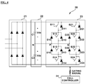
- FIG. 1 is a schematic view illustrating a serially-connected medium voltage inverter according to an exemplary embodiment of the present disclosure.
- an inverter (2) converts a 3-phase input power whose rms (root mean square) value is over 600V for a line-to-line voltage and supplies the converted power to a medium voltage 3-phase motor.
- the 3-phase motor may be an induction machine or a synchronous machine.
- the 3-phase motor may be other motors than the induction machine or the synchronous machine.
- the inverter (2) may include a phase shift transformer (10) and a plurality of power cells (20).
- the phase shift transformer (10) may insulate a power inputted form a power unit (1), and convert a phase and size of the voltage in response to demand from the plurality of power cells and provide the voltage to the plurality of power cells (20).
- a THD (Total Harmonic Distortion) of an input current can be enhanced by the phase shift.
- the plurality of power cells (20) may receive an output voltage of the phase shift transformer (10), and the output voltage of the medium voltage inverter (2) may be synthesized by a sum of outputs of power cells corresponding to each phase.
- an output voltage of a phase in the inverter (2) is a sum of output voltages of a serially-connected power cells ((20a1 and 20a2), an output voltage of b phase is a sum of output voltages of serially-connected power cells (20b1 and 20b2), and an output voltage of c phase is a sum of output voltages of serially-connected power cells (20c1 and 20c2).
- a serially-connected power cells ((20a1 and 20a2)
- an output voltage of b phase is a sum of output voltages of serially-connected power cells (20b1 and 20b2)
- an output voltage of c phase is a sum of output voltages of serially-connected power cells (20c1 and 20c2).
- the number of serially-connected power cells may be determined by an output voltage of the inverter (2).
- the plurality of power cells are formed in the same configuration, and reference numeral of power cells will be designated as '20' in the following description of the present disclosure.
- each synthesized output phase voltage of inverter (2) is same, there is a 120°phase difference between each output phase voltage. Furthermore, it should be apparent to the skilled in the art that THD of output voltage applied to the motor (3) and voltage change rate (dv/dt) can be improved by the increased number of power cells (20) forming the inverter (2) and various switching methods.
- FIG. 2 is a schematic block diagram illustrating power cells according to prior art.
- a power cell (200) includes a rectifying unit (210), a DC link capacitor (220), an inverter unit (230), a bypass switch (240) and a cell controller (250).
- the rectifying unit (210) is comprised of six diodes. Size of rectified DC link voltage is determined by a relation of a difference between an input power of the rectifying unit (210) and an output power of the power cell (200). A DC link voltage increases when a supplied input power is greater than a load-consumed output power, and a DC link voltage decreases in the reverse case.
- the DC link capacitor (220) is designed to solve an instantaneous power imbalance at input/output links.
- the inverter unit (230) is a mixture of NPC (Neutral-Point Clamped) method and an H-bridge method, where output voltages can be synthesized by turning on and turning off a plurality of switching elements from the DC link voltage.
- NPC Neutral-Point Clamped
- the cell controller (250) is independently arranged at each power cell and generates a gating signal that determines a switching state of a plurality of switching elements of the inverter unit (230).
- the bypass switch (240) serves to bypass an output voltage of the power cell (200) in response to control of the cell controller (250).
- the cell controller (250) transmits a fault signal to a master controller, transmits a bypass signal to the bypass switch (240) and short-circuits an output of a relevant power cell (200), such that no influence is exercised on operation of the motor (3), and a continued operation of inverter can be carried out using the normally operating power cells.
- An output voltage of power cell (200) in FIG. 2 may be determined by a voltage difference between Vu and Vv according to the following Equation 1.
- V uv V u ⁇ V v
- Vuv an output voltage of power cell
- Vu and Vv represent pole voltages.
- S11 and S13 in U phase switch, and S 12 and S14 perform a complementary switching operation of being alternately turned on and turned off, and likewise, S21 and S23 in V phase switch and S22 and S24 perform a complementary switching operation of being alternately turned on and turned off.
- a pole voltage and an output voltage of power cell (200) may be defined in response to switching state as shown in Table 1.
- FIG. 3 is a schematic view illustrating waveforms of an output voltage in an inverter unit of FIG.2 , which is an example of using an IPD (In-Phase Disposition) modulation.
- IPD In-Phase Disposition
- Command voltages Vm1 and Vm2 at two poles of a power cell (200) are same in frequency and size, and have a 180°phase difference. Although carrier waves Vcr1 and Vcr2 are same in frequency and size, offsets are different.
- Vcr1 when compared with pole voltage commands Vm1 and Vm2, generates gating signals of (S11, S 13) and (S21, S23), and Vcr2 generates gating signals of (S12, S14) and (S22, S24), when compared with pole voltage commands Vm1 and Vm2.
- NPC/H bridge inverter of inverter unit (230) in FIG. 3 uses a 3-level pole voltage as in Table 1, it outputs a 5-level voltage through Table 1. Each voltage level is same as that of Vdc.
- the bypass switch (240) is turned on during a bypass operation to short-circuit the output terminals Vu and Vv of the power cell (200). Because the output terminal is short-circuited, 0 is outputted at all times regardless of switching state of Table 1, and the cell controller (250) turns off all switches of power cells (200) in order to prevent arm short-circuit.
- bypass is realized by controlling the switching of switching elements in the inverter unit (23) without recourse to use of a separate bypass switch on the power cell according to the exemplary embodiment of the present disclosure.
- FIG. 4 is a detailed block diagram illustrating power cells of an inverter system according to an exemplary embodiment of the present disclosure.
- the power cell (20) may include a rectifying unit (21), a DC link capacitor (22), n inverter unit (23) and a cell controller (24).
- the rectifying unit (21) may be comprised of 6 diodes to rectify AC voltages respectively inputted from a phase shift transformer (10) to a DC. Size of the rectified DC link voltage may be determined by a relation of a difference between an input power of the rectifying unit (21) and an output power of power cell (20). W hen an input power supplied from the phase shift transformer (10) is greater than an output power consumed by a load, a DC link voltage may increase, but the DC link voltage may decrease in a reverse case.
- the DC link capacitor (22) may solve the instantaneous power imbalance of input/output terminals. Furthermore, the DC link capacitor (22) may be connected in series by first and second capacitors (C1, C2), where a voltage applied to each capacitor (C1, C2) corresponds to a DC link voltage. However, this configuration is exemplary, and the DC link capacitor may be configured by being connected by an increased number of capacitors.
- the inverter unit (23) is a mixture of an NPC method and an H-bridged method, where output voltages may be synthesized by turning on and turning off a plurality of switching elements from DC link voltages of DC link capacitor (22).
- the inverter unit (23) is configured in a manner such that a first switching element (S11) to a fourth switching element (S 14) may be serially connected, and a fifth switching element (S21) to eighth switching element (24) may be serially arranged.
- the first to fourth switching elements (S11 to S 14) are defined as a U phase switching element
- the fifth to eighth switching elements (S21 to S24) are defined as a V phase switching element.
- First to eighth diodes may be respectively connected in parallel to the switching elements. Furthermore ninth and tenth diodes (D 15, D16) may be serially connected to be connected in parallel to the connection between the second and third switching elements (S12, S 13), and a node (P) therebetween may be connected to a node (N) between the first and second capacitors (C1, C2). Furthermore, eleventh and twelfth diodes (D25, D26) are serially connected, and connected to a connection between sixth and seventh switching elements (S22, S24), and a node (Q) therebetween may be connected to a node (N) between the first and second capacitors (C1, C2).
- the node (N) between the first and second capacitors (C1, C2)), a node (P) between the ninth and tenth diodes (D 15, D16) and a node (Q) between the eleventh and twelfth diodes (D25, D26) may be respectively connected, which is called an NPC method.
- the cell controller (24) may be independently arranged for each power cell (20), and may generate a gating signal determining a switching state of a plurality of switching elements (23).
- bypass switch (240) is conventionally arranged at an output terminal of the power cell (200) and an output voltage is made 0 at all times by short-circuiting the bypass switch, and a path of a motor current is formed to carry out the bypass operation
- the cell controller (24) may output 0 voltage regardless of load current state to form a path of a motor current.
- a switching state of a power cell outputting 0 at all times may be defined by the following Table 2.
- the cell controller (24) changes adjacently arranged four switching elements among U phase and V phase switching elements to an ON state in an inverter unit (23) in which a plurality of switching elements and a plurality of diodes are arranged in an NPC/H bridge method.
- two U phase switching elements and two V phase switching elements are changed to ON state, and at this time, the ON state changed U phase and V phase switching elements are arranged at respectively corresponding positions.
- an output voltage may be 0, whereby a bypass can be formed.
- FIGS. 5, 6 and 7 are schematic views illustrating a path of an output current for each mode of Table 2, where FIG 5 corresponds to a mode 1 of Table 2, in which the first, second, fifth and sixth switching elements (S11, S12, S21 S22) are made in ON state to perform a bypass operation.
- a current can be bypassed by forming a close circuit along a path of D12 ⁇ D11 ⁇ S21 ⁇ S22 when the current is in a positive (+) direction, which is illustrated in a solid line.
- a current can be bypassed by forming a close circuit along a path of D22 ⁇ D21 ⁇ S11 ⁇ S12 when the current is in a negative (-) direction, which is illustrated in a dotted line.
- FIG. 6 corresponds to mode 2 of Table 2, where the second, third, sixth and seventh switching elements (S12, S 13, S22 S23) are made in ON state to carry out a bypass operation.
- a current may be bypassed along a path of S13 ⁇ D16 ⁇ D25 ⁇ S22 when the current is in a positive direction, which is illustrated in a solid line. Conversely, a current may be bypassed along a path of S23 ⁇ D26 ⁇ D15 ⁇ S12 when the current is in a negative direction, which is illustrated in a dotted line.
- FIG. 7 corresponds to mode 3 in Table 2, and illustrates that a bypass operation is carried out by making the third, fourth, seventh and eighth switching elements in ON state.
- a current may be bypassed along a path of S13 ⁇ S14 ⁇ D24 ⁇ D23 when the current is in a positive direction, which is illustrated in a solid line. Conversely, a current may be bypassed along a path of S23 ⁇ S24 ⁇ D14 ⁇ D13 when the current is in a negative direction, which is illustrated in a dotted line.
- the cell controller (24) may control ON and/or OFF of the switching elements to carry out a bypass operation not affecting an entire medium voltage inverter through a 0 output voltage, by short-circuiting an output terminal of the inverter unit (23) while a load current is made not to flow to a DC link power of the power cell (20) regardless of current direction.
- the NPC/H bridge inverter may use three bypassable switching states thus discussed, such that bypass switching states adequate to positions of faulted switching elements may be set up as in the following Table 3.
- Table 3 Faulted switching element Useable bypass modes 1 Fault generated among S13, S14, S23, S24 Mode 1 2 Fault generated among S11, S14, S21, S24 Mode 2 3 Fault generated among S11, S12, S21, S22 Mode 3
- the first, second fifth and sixth switching elements S11, S12, S21, S22
- a bypass operation can be performed using a bypass mode 1
- the second, third, sixth and seventh switching elements S12, S13, S22, S23
- the third, fourth, seventh and eighth switching elements can perform a normal operation, and a bypass operation can be performed using a bypass mode 3.
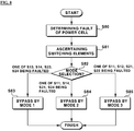
- FIG. 8 is a flowchart illustrating to explain the performance of bypass operation by a cell controller of the present disclosure determining a bypass mode.
- a cell controller (24) may ascertain a state of each switching element in the inverter unit (23) when it is determined that a fault is generated from a power cell (20) (S80), the cell controller (24) may ascertain a state of each switching element in the inverter unit (23)(S81), select a mode in response to the fault of switching element (S82) and carry out a bypass operation (S83 to S85).
- the cell controller (24) may perform a bypass operation using a bypass mode 1 when any one of the third, fourth, seventh and eighth switching elements is developed with a fault (S83), the cell controller (24) may perform a bypass operation using a bypass mode 2 when any one of the first, fourth, fifth and eighth switching elements (S11, S14, S21, S24) is developed with a fault (S84), and the cell controller (24) may perform a bypass operation using a bypass mode 3 when any one of first, second, fifth and sixth switching elements (S11, S12, S21, S22) is developed with a fault (S85).
- the present disclosure has an industrial applicability in that switching operations of switching elements in an inverter unit can be controlled to allow a current to bypass, whereby a manufacturing cost can be reduced because of no use of additional switch, when a cell controller (24) determines that a power cell is developed with a fault.
Landscapes
- Engineering & Computer Science (AREA)
- Power Engineering (AREA)
- Inverter Devices (AREA)
Applications Claiming Priority (1)
| Application Number | Priority Date | Filing Date | Title |
|---|---|---|---|
| KR1020150033017A KR20160109137A (ko) | 2015-03-10 | 2015-03-10 | 인버터 시스템 |
Publications (1)
| Publication Number | Publication Date |
|---|---|
| EP3068029A1 true EP3068029A1 (de) | 2016-09-14 |
Family
ID=55484903
Family Applications (1)
| Application Number | Title | Priority Date | Filing Date |
|---|---|---|---|
| EP16158904.9A Withdrawn EP3068029A1 (de) | 2015-03-10 | 2016-03-07 | Umrichtersystem |
Country Status (5)
| Country | Link |
|---|---|
| US (1) | US20160268948A1 (de) |
| EP (1) | EP3068029A1 (de) |
| JP (1) | JP2016171742A (de) |
| KR (1) | KR20160109137A (de) |
| CN (1) | CN105978357A (de) |
Cited By (2)
| Publication number | Priority date | Publication date | Assignee | Title |
|---|---|---|---|---|
| EP3648331A4 (de) * | 2017-06-27 | 2020-07-08 | Mitsubishi Electric Corporation | Stromwandlungsvorrichtung |
| CN113661643A (zh) * | 2019-02-28 | 2021-11-16 | 艾思玛太阳能技术股份公司 | 用于在多电平逆变器的交变电流输出端发生瞬态电压变化的情况下进行电流限制的方法以及多电平逆变器 |
Families Citing this family (12)
| Publication number | Priority date | Publication date | Assignee | Title |
|---|---|---|---|---|
| US9425705B2 (en) | 2012-08-13 | 2016-08-23 | Rockwell Automation Technologies, Inc. | Method and apparatus for bypassing cascaded H-bridge (CHB) power cells and power sub cell for multilevel inverter |
| KR20150140966A (ko) * | 2014-06-09 | 2015-12-17 | 엘에스산전 주식회사 | 바이패스 운전 기능을 갖는 직렬형 h-브릿지 인버터 |
| KR102485705B1 (ko) * | 2016-02-18 | 2023-01-05 | 엘에스일렉트릭(주) | 멀티 레벨 인버터의 3상 평형 전압 제어 방법 |
| EP3533208B1 (de) * | 2016-10-31 | 2024-06-12 | Telefonaktiebolaget LM Ericsson (PUBL) | Einsatz von akteurinstanzen |
| CN107204630B (zh) * | 2017-06-09 | 2018-04-17 | 湖南大学 | 兼具快速动态响应的海岛npc型电源高精度控制方法 |
| JP2020529184A (ja) * | 2017-09-25 | 2020-10-01 | エルエス、エレクトリック、カンパニー、リミテッドLs Electric Co., Ltd. | インバータシステム |
| US10158299B1 (en) | 2018-04-18 | 2018-12-18 | Rockwell Automation Technologies, Inc. | Common voltage reduction for active front end drives |
| CN108521234A (zh) * | 2018-04-26 | 2018-09-11 | 南京理工大学 | 一种二极管钳位与级联混合式五电平逆变器 |
| US11211879B2 (en) | 2019-09-23 | 2021-12-28 | Rockwell Automation Technologies, Inc. | Capacitor size reduction and lifetime extension for cascaded H-bridge drives |
| US11791760B2 (en) * | 2021-02-10 | 2023-10-17 | Regal Beloit America, Inc. | Systems and methods for component monitoring in an electric motor |
| US11342878B1 (en) | 2021-04-09 | 2022-05-24 | Rockwell Automation Technologies, Inc. | Regenerative medium voltage drive (Cascaded H Bridge) with reduced number of sensors |
| CN114002540B (zh) * | 2021-09-23 | 2024-05-28 | 南京国电南自电网自动化有限公司 | 配电网线路发展性故障保护方法及系统 |
Citations (2)
| Publication number | Priority date | Publication date | Assignee | Title |
|---|---|---|---|---|
| US20140078797A1 (en) * | 2012-09-18 | 2014-03-20 | Siemens Corporation | Control for fault-bypass of cascaded multi-level inverter |
| US20140085954A1 (en) * | 2011-01-12 | 2014-03-27 | Kabushiki Kaisha Toshiba | Semiconductor power conversion device |
Family Cites Families (8)
| Publication number | Priority date | Publication date | Assignee | Title |
|---|---|---|---|---|
| JP4070121B2 (ja) * | 2003-05-29 | 2008-04-02 | 三菱電機株式会社 | 電力変換装置 |
| JP5145124B2 (ja) * | 2008-06-09 | 2013-02-13 | 株式会社日立製作所 | 電力変換装置 |
| JP2010220332A (ja) * | 2009-03-16 | 2010-09-30 | Toshiba Mitsubishi-Electric Industrial System Corp | 電力変換装置 |
| JP5664966B2 (ja) * | 2011-01-14 | 2015-02-04 | 株式会社安川電機 | 直列多重電力変換装置 |
| CN103001573B (zh) * | 2011-09-13 | 2016-03-23 | 台达电子企业管理(上海)有限公司 | 中压变频驱动系统 |
| US8982587B2 (en) * | 2012-04-23 | 2015-03-17 | Hamilton Sundstrand Corporation | Compensating ripple on pulse with modulator outputs |
| CN103795323A (zh) * | 2012-11-02 | 2014-05-14 | 上海电气集团股份有限公司 | 一种高压变频调速系统及其控制方法 |
| CN103606946B (zh) * | 2013-11-25 | 2016-04-20 | 国家电网公司 | 一种基于mmc提升交流架空线路输送能力的输电系统 |
-
2015
- 2015-03-10 KR KR1020150033017A patent/KR20160109137A/ko not_active Withdrawn
-
2016
- 2016-03-07 EP EP16158904.9A patent/EP3068029A1/de not_active Withdrawn
- 2016-03-08 US US15/064,390 patent/US20160268948A1/en not_active Abandoned
- 2016-03-10 JP JP2016046996A patent/JP2016171742A/ja active Pending
- 2016-03-10 CN CN201610137718.4A patent/CN105978357A/zh active Pending
Patent Citations (2)
| Publication number | Priority date | Publication date | Assignee | Title |
|---|---|---|---|---|
| US20140085954A1 (en) * | 2011-01-12 | 2014-03-27 | Kabushiki Kaisha Toshiba | Semiconductor power conversion device |
| US20140078797A1 (en) * | 2012-09-18 | 2014-03-20 | Siemens Corporation | Control for fault-bypass of cascaded multi-level inverter |
Cited By (3)
| Publication number | Priority date | Publication date | Assignee | Title |
|---|---|---|---|---|
| EP3648331A4 (de) * | 2017-06-27 | 2020-07-08 | Mitsubishi Electric Corporation | Stromwandlungsvorrichtung |
| US10992219B2 (en) | 2017-06-27 | 2021-04-27 | Mitsubishi Electric Corporation | Power conversion device |
| CN113661643A (zh) * | 2019-02-28 | 2021-11-16 | 艾思玛太阳能技术股份公司 | 用于在多电平逆变器的交变电流输出端发生瞬态电压变化的情况下进行电流限制的方法以及多电平逆变器 |
Also Published As
| Publication number | Publication date |
|---|---|
| KR20160109137A (ko) | 2016-09-21 |
| US20160268948A1 (en) | 2016-09-15 |
| CN105978357A (zh) | 2016-09-28 |
| JP2016171742A (ja) | 2016-09-23 |
Similar Documents
| Publication | Publication Date | Title |
|---|---|---|
| EP3068029A1 (de) | Umrichtersystem | |
| JP6227041B2 (ja) | マルチレベルインバータ | |
| KR101189428B1 (ko) | 전력 변환 장치 | |
| KR101791289B1 (ko) | 멀티레벨 인버터 | |
| US9325252B2 (en) | Multilevel converter systems and sinusoidal pulse width modulation methods | |
| CN101542867B (zh) | 大功率应用的电力电子变换器 | |
| KR101769176B1 (ko) | 멀티레벨 인버터 시스템 | |
| US20140198548A1 (en) | System and method for power conversion | |
| US9214875B2 (en) | Multilevel inverter | |
| EP3093976B1 (de) | Elektrisches stromwandlersystem | |
| US20150357939A1 (en) | Cascaded h-bridge inverter capable of operating in bypass mode | |
| JP5362657B2 (ja) | 電力変換装置 | |
| US20180091058A1 (en) | Multiphase multilevel power converter, control apparatus and methods to control harmonics during bypass operation | |
| CN106160540A (zh) | 电力变换装置 | |
| KR20210063210A (ko) | 그리드 유형에 무관한 효율적인 dc 링크 처리를 위한 장치 | |
| JP6111726B2 (ja) | マルチレベル電力変換回路の制御方式 | |
| EP3691107A1 (de) | Umrichtersystem | |
| KR102261327B1 (ko) | 인버터 시스템 | |
| Carpaneto et al. | A new cascaded multilevel converter based on NPC cells | |
| KR101224589B1 (ko) | 멀티레벨 인버터 | |
| JP2015015778A (ja) | 系統連系用電力変換システム | |
| CN117730476A (zh) | 具有多种运行模式的基于单元的多电平转换器和相关联的控制方法 | |
| KR102261330B1 (ko) | 인버터 시스템 |
Legal Events
| Date | Code | Title | Description |
|---|---|---|---|
| PUAI | Public reference made under article 153(3) epc to a published international application that has entered the european phase |
Free format text: ORIGINAL CODE: 0009012 |
|
| AK | Designated contracting states |
Kind code of ref document: A1 Designated state(s): AL AT BE BG CH CY CZ DE DK EE ES FI FR GB GR HR HU IE IS IT LI LT LU LV MC MK MT NL NO PL PT RO RS SE SI SK SM TR |
|
| AX | Request for extension of the european patent |
Extension state: BA ME |
|
| 17P | Request for examination filed |
Effective date: 20170308 |
|
| RBV | Designated contracting states (corrected) |
Designated state(s): AL AT BE BG CH CY CZ DE DK EE ES FI FR GB GR HR HU IE IS IT LI LT LU LV MC MK MT NL NO PL PT RO RS SE SI SK SM TR |
|
| STAA | Information on the status of an ep patent application or granted ep patent |
Free format text: STATUS: THE APPLICATION HAS BEEN WITHDRAWN |
|
| 18W | Application withdrawn |
Effective date: 20180502 |