EP3070848A1 - Circuit de porte non-et, panneau arrière d'affichage, affichage et dispositif électronique - Google Patents
Circuit de porte non-et, panneau arrière d'affichage, affichage et dispositif électronique Download PDFInfo
- Publication number
- EP3070848A1 EP3070848A1 EP14859294.2A EP14859294A EP3070848A1 EP 3070848 A1 EP3070848 A1 EP 3070848A1 EP 14859294 A EP14859294 A EP 14859294A EP 3070848 A1 EP3070848 A1 EP 3070848A1
- Authority
- EP
- European Patent Office
- Prior art keywords
- electrode
- transistor
- pull
- input
- level
- Prior art date
- Legal status (The legal status is an assumption and is not a legal conclusion. Google has not performed a legal analysis and makes no representation as to the accuracy of the status listed.)
- Granted
Links
Images
Classifications
-
- H—ELECTRICITY
- H03—ELECTRONIC CIRCUITRY
- H03K—PULSE TECHNIQUE
- H03K19/00—Logic circuits, i.e. having at least two inputs acting on one output; Inverting circuits
- H03K19/0175—Coupling arrangements; Interface arrangements
- H03K19/0185—Coupling arrangements; Interface arrangements using field effect transistors only
- H03K19/018507—Interface arrangements
-
- H—ELECTRICITY
- H03—ELECTRONIC CIRCUITRY
- H03K—PULSE TECHNIQUE
- H03K19/00—Logic circuits, i.e. having at least two inputs acting on one output; Inverting circuits
- H03K19/02—Logic circuits, i.e. having at least two inputs acting on one output; Inverting circuits using specified components
- H03K19/08—Logic circuits, i.e. having at least two inputs acting on one output; Inverting circuits using specified components using semiconductor devices
- H03K19/094—Logic circuits, i.e. having at least two inputs acting on one output; Inverting circuits using specified components using semiconductor devices using field-effect transistors
- H03K19/0944—Logic circuits, i.e. having at least two inputs acting on one output; Inverting circuits using specified components using semiconductor devices using field-effect transistors using MOSFET or insulated gate field-effect transistors, i.e. IGFET
- H03K19/09441—Logic circuits, i.e. having at least two inputs acting on one output; Inverting circuits using specified components using semiconductor devices using field-effect transistors using MOSFET or insulated gate field-effect transistors, i.e. IGFET of the same canal type
- H03K19/09443—Logic circuits, i.e. having at least two inputs acting on one output; Inverting circuits using specified components using semiconductor devices using field-effect transistors using MOSFET or insulated gate field-effect transistors, i.e. IGFET of the same canal type using a combination of enhancement and depletion transistors
- H03K19/09445—Logic circuits, i.e. having at least two inputs acting on one output; Inverting circuits using specified components using semiconductor devices using field-effect transistors using MOSFET or insulated gate field-effect transistors, i.e. IGFET of the same canal type using a combination of enhancement and depletion transistors with active depletion transistors
-
- H—ELECTRICITY
- H03—ELECTRONIC CIRCUITRY
- H03K—PULSE TECHNIQUE
- H03K19/00—Logic circuits, i.e. having at least two inputs acting on one output; Inverting circuits
- H03K19/20—Logic circuits, i.e. having at least two inputs acting on one output; Inverting circuits characterised by logic function, e.g. AND, OR, NOR, NOT circuits
Definitions
- the present disclosure relates to the field of display technology, in particular to an NAND gate circuit, a display back plate, a display device and an electronic device.
- an a-Si TFT thin film transistor
- a LTPS low temperature poly-silicon
- oxide TFT display device e.g., an oxide TFT (thin film transistor) display device, a LTPS (low temperature poly-silicon) TFT display device, or an oxide TFT display device.
- An a-Si TFT has such drawbacks as low migration rate and poor stability, while an LTPS TFT is not adapted to the manufacture of a large-size panel.
- an oxide TFT usually has a depleted I-V transfer characteristic, i.e., the oxide TFT remains in an on state when its gate-to-source voltage Vgs is zero.
- An NAND gate is a logic circuit commonly used for digital circuits.
- For the two-input NAND gate when two input signals are both at a high level, an output signal is at a low level, and when merely one input signal is at a high level and the other one is at a low level, the output signal is at a high level.
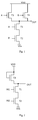
- a commonly-used NAND gate circuit mainly consists of CMOS (complementary metal oxide semiconductor) circuits, in which two N-type TFTs for providing the input signals are connected in series and two P-type TFTs for providing the input signals are connected in parallel.
- A represents a first input signal
- B represents a second input signal
- Out represents an output signal
- VDD represents a high level
- VSS represents a low level.
- the CMOS circuit has such advantages as small leakage current and low power consumption.
- a TFT such as the oxide TFT
- T1, T2 and T3 represent a first N-type TFT, a second N-type TFT and a third N-type TFT, respectively, IN1 and IN2 represent the first input signal and the second input signal, respectively, OUT represents the output signal, VDD represents the high level and VSS represents the low level.
- T3 works as a diode and functions as a pull-up resistor. When IN1 and IN2 are at a high level, T1 and T2 are turned on simultaneously so as to pull down OUT. However, T3 remains in the on state all the time, so there is a DC path from VDD to VSS.
- an output low level is determined by the voltage division of series resistances between T3 and T1 as well as T2, and thus it cannot reach the low level VSS.
- T1 and T2 are cut off.
- T3 works as the diode
- OUT is equal to VDD-VTH (a threshold voltage of T3). At this time, OUT cannot reach the high level VDD either.
- an NAND gate of a traditional NMOS (N-metal-oxide-semiconductor) structure also has a large leakage current, and cannot be used to achieve a rail-to-rail output.
- a main object of the present disclosure is to provide an NAND gate circuit, a display back plate, a display device, and an electronic device, so as to achieve lossless transmission and a rail-to-rail output via an NAND gate when an input TFT is a depleted TFT.
- the present disclosure provides an NAND gate circuit, including at least two input transistors, a gate electrode of each input transistor being connected to an input signal, a first electrode of a first input transistor being connected to an NAND gate output end, a second electrode of a last input transistor being connected to a first level, and apart from the last input transistor, a second electrode of each input transistor being connected to a first electrode of a next input transistor, wherein the NAND gate circuit further includes at least two pull-up modules and at least two input control transistors, a gate electrode of each input control transistor is connected to the input signal, a first electrode thereof is connected to a control end of the corresponding pull-up module, and a second electrode thereof is connected to the first level, the first electrode of the first input transistor is connected to a second level output end via the pull-up module, the input control transistor is configured to enable a potential of the control end of the pull-up module connected to the first electrode of the input transistor to be the first level when the input signal connected to the gate electrode of the input control transistor is at
- the at least two input transistors and the at least two input control transistors are all depleted NMOS transistors, the first electrode is a source electrode, the second electrode is a drain electrode, the second level is a high level, and the first level is a low level.
- the at least two input transistors and the at least two input control transistors are all depleted PMOS transistors, the first electrode is a drain electrode, the second electrode is a source electrode, the second level is a low level, and the first level is a high level.
- the pull-up module includes a first pull-up transistor, a second pull-up transistor and a storage capacitor, wherein a gate electrode of the second pull-up transistor is the control end of the pull-up module, a gate electrode of the first pull-up transistor is connected to the second level output end, a first electrode of the first pull-up transistor is connected to the gate electrode of the first pull-up transistor, and a second electrode of the first pull-up transistor is connected to the gate electrode of the second pull-up transistor, a first electrode of the second pull-up transistor is connected to the second level output end, and a second electrode thereof is connected to the NAND gate output end, and the storage capacitor is connected between the gate electrode and the second electrode of the second pull-up transistor.
- the first pull-up transistor and the second pull-up transistor are both depleted NMOS transistors.
- the first pull-up transistor and the second pull-up transistor are both depleted PMOS transistors.
- the present disclosure provides a display back plate including the above-mentioned NAND gate circuit.
- the present disclosure provides a display device including the above-mentioned display back plate.
- the present disclosure provides an electronic device including the above-mentioned NAND gate circuit.
- the input control transistors and the pull-up modules are adopted so as to ensure lossless transmission and rail-to-rail output via the NAND gate when the input transistors are depleted TFTs, thereby to reduce the leakage current as well as improve the stability and speed of the NAND gate circuit.
- the source electrode is symmetric with its drain electrode, so there is no difference therebetween.
- one electrode of the TFT is called as source electrode while the other is called as drain electrode, so as to differentiate them from each other.
- the transistors may be divided into NMOS transistors and PMOS transistors.
- the NMOS transistor is taken as an example.
- the PMOS transistor may also be used, and they also fall within the scope of the present disclosure.
- An NAND gate circuit of the present disclosure includes at least two input transistors.
- a gate electrode of each input transistor is connected to an input signal
- a first electrode of a first input transistor is connected to an NAND gate output end
- a second electrode of a last input transistor is connected to a first level, and apart from the last input transistor
- a second electrode of each input transistor is connected to a first electrode of a next input transistor.
- the NAND gate circuit further includes at least two pull-up modules and at least two input control transistors.
- a gate electrode of each input control transistor is connected to one input signal, a first electrode thereof is connected to a control end of the corresponding pull-up module, and a second electrode thereof is connected to the first level.
- the first electrode of the first input transistor is connected to a second level output end via the pull-up module.
- the input control transistor is configured to enable a potential of the control end of the pull-up module connected to the first electrode of the input transistor to be the first level when the input signal connected to the gate electrode of the input control transistor is at a second level.
- the at least two pull-up modules are configured to cut off the connection between the second level output end and the NAND gate output end when all the input signals are at the second level, and enable the connection between the second level output end and the NAND gate output end when none of the input signals is at the second level.
- the input control transistors and the pull-up modules are adopted so as to ensure lossless transmission and rail-to-rail output via the NAND gate when the input transistors are depleted TFTs, thereby to reduce the leakage current as well as improve the stability and speed of the NAND gate circuit.
- the at least two input transistors and the at least two input control transistors are all depleted NMOS transistors, and at this time, the first electrode is a source electrode, the second electrode is a drain electrode, the second level is a high level, and the first level is a low level.
- the at least two input transistors and the at least two input control transistors are all depleted PMOS transistors, and at this time, the first electrode is a drain electrode, the second electrode is a source electrode, the second level is a low level, and the first level is a high level.
- the NMOS transistors are taken as an example.
- a first electrode of the NMOS transistor may be a source electrode, a second electrode thereof may be a drain electrode, the second level may be a high level, and the first level may be a low level.
- the PMOS transistors may also be used, and they also fall within the scope of the present disclosure.
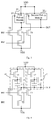
- the NAND gate circuit includes:
- the NAND gate circuit further includes a first pull-up module 31 and a second pull-up module 32.
- a source electrode of the first input control transistor T3 is connected to a control end D1 of the first pull-up module 31, and a source electrode of the second input control transistor T4 is connected to a control end D2 of the second pull-up module 32.
- the source electrode of the first input transistor T1 is connected to a high level output end, which outputs a high level VDD, via the first pull-up module 31, and the source electrode of the first input transistor T1 is also connected to the high level output end via the second pull-up module 32.
- the first pull-up module 31 and the second pull-up module 32 are configured to cut off the connection between the high level output end and the NAND gate output end OUT when both the first input signal IN1 and the second input signal IN2 are at a high level, so as to cut off a charge current from the high level output end to the NAND gate output end OUT, thereby to enable an output signal from the NAND gate output end OUT to reach the low level VSS output by a low level output end.
- the first pull-up module 31 and the second pull-up module 32 are further configured to enable the connection between the high level output end and the NAND gate output end OUT when neither of the first input signal IN1 and the second input signal IN2 is at the high level, so as to enable the lossless transmission from the high level VDD to the NAND gate output end OUT.
- T1, T2, T3 and T4 are all depleted NMOS transistors.
- T3 is used to control a potential of D1 to be a low level
- T4 is used to control a potential of D2 to be a low level too, so as to cut off the connection between the high level output end and OUT.
- T3 is used to control the potential of D1 to be a low level while T4 is turned off, so as to achieve the lossless transmission from VDD to OUT under the control of the second pull-up module 32.
- T4 is used to control the potential of D2 to be a low level while T3 is turned off, so as to achieve the lossless transmission from VDD to OUT under the control of the first pull-up module 31.
- the pull-up module includes a first pull-up transistor, a second pull-up transistor and a storage capacitor.
- a gate electrode of the second pull-up transistor is a control end of the pull-up module.
- a gate electrode of the first pull-up transistor is connected to the second level output end, a first electrode of the first pull-up transistor is connected to the gate electrode of the first pull-up transistor, and a second electrode thereof is connected to the gate electrode of the second pull-up transistor.
- a first electrode of the second pull-up transistor is connected to the second level output end, and a second electrode thereof is connected to the NAND gate output end.
- the storage capacitor is connected between the gate electrode and the second electrode of the second pull-up transistor.
- the first pull-up transistor and the second pull-up transistor are both depleted NMOS transistors.
- the first pull-up transistor and the second pull-up transistor are both depleted PMOS transistors.
- the NAND gate circuit of the present disclosure includes:
- the first pull-up module 41 includes:
- the second pull-up module 42 includes:
- T1, T2, T3, T4, T5, T6, T7 and T8 are all depleted NMOS transistors.
- T1 and T2 are turned on simultaneously so as to pull down the output signal
- T3 and T4 are turned on too so as to pull down gate voltages of T6 and T7 to a low level
- T6 and T8 are turned off so as to cut off a charge current from the high level output end, which outputs the high level VDD, to the NAND gate output end OUT.
- the output signal may reach the low level VSS.
- T1 When IN1 is at a high level and IN2 is at a low level, T1 is turned on, T2 is turned off so as to cut off a pull-down path of the NAND gate output end OUT, T3 is turned on, T4 is turned off, T7, worked as a diode, is turned on, and C2 is charged by VDD through T7 so as to raise a potential at the gate electrode of T8, thereby to turn on T8 and transmit a high level to OUT.
- C2 Along with an increase in a voltage of OUT, C2 is continuously charged by VDD through T7, so as to continuously raise the potential at the gate electrode of T8 until it reach a positive voltage exceeding VDD+VTH8 (a threshold voltage of T8), thereby to fully turn on T8.
- VDD+VTH8 a threshold voltage of T8
- T1 When IN1 is at a low level and IN2 is at a high level, T1 is turned off and T2 is turned on so as to cut off a pull-down path of the NAND gate output end, T4 is turned on, T3 is turned off, T5, worked as a diode, is turned on, and C1 is charged by VDD through T5 so as to raise a potential at the gate electrode of T6, thereby to turn on T6 and transmit a high level to OUT.
- VDD+VTH6 a threshold voltage of T6
- T5 and T6 may be of a very small W/L (a ratio of width to length). In this way, when OUT outputs a low level, the gate electrode of T6 is at a low level, and an leakage current of T6 being in an off state is far less than an static current of T3 being in an on state in Fig.2 . In addition, due to a very small size of T5, a sum of static currents of T5 and T6 being in on states is far less than the static current of T3 being in an on state in Fig.2 too, and as a result, the leakage current is reduced. The same condition will occur for T7, T8 and T5, T6 in Fig.4 , and thus it will not be repeated herein.
- a capacitance bootstrapping structure consisting of eight TFTs and two capacitors is adopted, so as to achieve the rail-to-rail output and the full voltage swing, and achieve the lossless transmission, thereby to reduce the leakage current as well as improve the stability and speed of the NAND gate circuit.
- the present disclosure further provides a display back plate including the above-mentioned NAND gate circuit.
- the present disclosure further provides a display device including the above-mentioned display back plate.
- the present disclosure further provides an electronic device including the above-mentioned NAND gate circuit.
Landscapes
- Engineering & Computer Science (AREA)
- Computer Hardware Design (AREA)
- Physics & Mathematics (AREA)
- Computing Systems (AREA)
- General Engineering & Computer Science (AREA)
- Mathematical Physics (AREA)
- Power Engineering (AREA)
- Logic Circuits (AREA)
Applications Claiming Priority (2)
| Application Number | Priority Date | Filing Date | Title |
|---|---|---|---|
| CN201310573352.1A CN103560782B (zh) | 2013-11-15 | 2013-11-15 | 与非门电路、显示器背板和显示器 |
| PCT/CN2014/083725 WO2015070647A1 (fr) | 2013-11-15 | 2014-08-05 | Circuit de porte non-et, panneau arrière d'affichage, affichage et dispositif électronique |
Publications (3)
| Publication Number | Publication Date |
|---|---|
| EP3070848A1 true EP3070848A1 (fr) | 2016-09-21 |
| EP3070848A4 EP3070848A4 (fr) | 2017-08-02 |
| EP3070848B1 EP3070848B1 (fr) | 2019-10-02 |
Family
ID=50014961
Family Applications (1)
| Application Number | Title | Priority Date | Filing Date |
|---|---|---|---|
| EP14859294.2A Active EP3070848B1 (fr) | 2013-11-15 | 2014-08-05 | Circuit de porte non-et, panneau arrière d'affichage, affichage et dispositif électronique |
Country Status (4)
| Country | Link |
|---|---|
| US (1) | US9325315B2 (fr) |
| EP (1) | EP3070848B1 (fr) |
| CN (1) | CN103560782B (fr) |
| WO (1) | WO2015070647A1 (fr) |
Cited By (1)
| Publication number | Priority date | Publication date | Assignee | Title |
|---|---|---|---|---|
| CN110690889A (zh) * | 2019-10-14 | 2020-01-14 | 华南理工大学 | 一种电平移位电路 |
Families Citing this family (7)
| Publication number | Priority date | Publication date | Assignee | Title |
|---|---|---|---|---|
| CN103560782B (zh) * | 2013-11-15 | 2015-04-22 | 京东方科技集团股份有限公司 | 与非门电路、显示器背板和显示器 |
| CN104575425B (zh) * | 2015-01-09 | 2017-04-12 | 深圳市华星光电技术有限公司 | 扫描驱动电路及其与非门逻辑运算电路 |
| CN104883181B (zh) * | 2015-06-10 | 2018-03-16 | 京东方科技集团股份有限公司 | 或非门电路、移位寄存器、阵列基板及显示装置 |
| FI20150294A (fi) * | 2015-10-23 | 2017-04-24 | Ari Paasio | Matalan tehonkulutuksen logiikkaperhe |
| US11831309B2 (en) | 2018-04-20 | 2023-11-28 | Texas Instruments Incorporated | Stress reduction on stacked transistor circuits |
| US11626875B2 (en) * | 2018-04-20 | 2023-04-11 | Texas Instruments Incorporated | Stress reduction on stacked transistor circuits |
| CN108735163B (zh) * | 2018-05-30 | 2020-11-17 | 京东方科技集团股份有限公司 | 用于阵列基板行驱动单元的或逻辑运算电路 |
Family Cites Families (11)
| Publication number | Priority date | Publication date | Assignee | Title |
|---|---|---|---|---|
| US6392486B1 (en) * | 2001-08-14 | 2002-05-21 | Xilinx, Inc. | Low-noise common-gate amplifier for wireless communications |
| KR100498453B1 (ko) * | 2002-11-04 | 2005-07-01 | 삼성전자주식회사 | 출력 데이터의 스큐를 감소시킬 수 있는 출력버퍼 회로 |
| US7061279B1 (en) | 2004-12-30 | 2006-06-13 | Broadcom Corporation | System and method for high frequency, high output swing buffers |
| CN1835402B (zh) | 2005-03-15 | 2010-04-28 | 凌阳科技股份有限公司 | 自偏压式高频逻辑门与应用其的或非门、与非门 |
| US8013633B2 (en) * | 2007-06-20 | 2011-09-06 | Hewlett-Packard Development Company, L.P. | Thin film transistor logic |
| CN101354924B (zh) | 2007-07-23 | 2013-03-13 | 奇晶光电股份有限公司 | 移位寄存器电路与其上拉单元 |
| JP2010098666A (ja) | 2008-10-20 | 2010-04-30 | Seiko Epson Corp | 排他的論理和回路および電気光学装置 |
| CN101547004B (zh) | 2009-05-12 | 2011-06-15 | 威盛电子股份有限公司 | 与门电路 |
| US8570066B2 (en) * | 2011-03-24 | 2013-10-29 | Electronics And Telecommunications Research Institute | Inverter, NAND gate, and NOR gate |
| TWI488163B (zh) * | 2013-01-23 | 2015-06-11 | Au Optronics Corp | 移位暫存器、使用該移位暫存器之閘極驅動電路與顯示裝置 |
| CN103560782B (zh) | 2013-11-15 | 2015-04-22 | 京东方科技集团股份有限公司 | 与非门电路、显示器背板和显示器 |
-
2013
- 2013-11-15 CN CN201310573352.1A patent/CN103560782B/zh active Active
-
2014
- 2014-08-05 EP EP14859294.2A patent/EP3070848B1/fr active Active
- 2014-08-05 WO PCT/CN2014/083725 patent/WO2015070647A1/fr not_active Ceased
- 2014-08-05 US US14/420,880 patent/US9325315B2/en active Active
Cited By (1)
| Publication number | Priority date | Publication date | Assignee | Title |
|---|---|---|---|---|
| CN110690889A (zh) * | 2019-10-14 | 2020-01-14 | 华南理工大学 | 一种电平移位电路 |
Also Published As
| Publication number | Publication date |
|---|---|
| WO2015070647A1 (fr) | 2015-05-21 |
| US9325315B2 (en) | 2016-04-26 |
| EP3070848A4 (fr) | 2017-08-02 |
| CN103560782B (zh) | 2015-04-22 |
| EP3070848B1 (fr) | 2019-10-02 |
| US20160028398A1 (en) | 2016-01-28 |
| CN103560782A (zh) | 2014-02-05 |
Similar Documents
| Publication | Publication Date | Title |
|---|---|---|
| EP3070848B1 (fr) | Circuit de porte non-et, panneau arrière d'affichage, affichage et dispositif électronique | |
| EP4036900A1 (fr) | Unité de registre à décalage, procédé d'attaque, circuit d'attaque de grille et dispositif d'affichage | |
| EP3614369B1 (fr) | Circuit d'attaque de balayage | |
| KR101944640B1 (ko) | Igzo 프로세스 기반인 게이트 전극 구동회로 | |
| CN104464662B (zh) | 基于低温多晶硅半导体薄膜晶体管的goa电路 | |
| KR101944641B1 (ko) | Igzo 프로세스 기반인 게이트 전극 구동회로 | |
| CN106847195B (zh) | 栅极线驱动电路 | |
| US9620073B2 (en) | Liquid crystal display device and gate driving circuit thereof | |
| WO2016197523A1 (fr) | Circuit de porte non-ou, registre à décalage, substrat de matrice et dispositif d'affichage | |
| WO2016095300A1 (fr) | Circuit de pilotage d'électrode de grille | |
| CN104575425B (zh) | 扫描驱动电路及其与非门逻辑运算电路 | |
| US20160343337A1 (en) | Scan Driving Circuit and NOR Gate Logic Operation Circuit Thereof | |
| KR101943234B1 (ko) | 저온 폴리 실리콘 반도체 박막 트랜지스터 기반 goa회로 | |
| CN104464656A (zh) | 基于低温多晶硅半导体薄膜晶体管的goa电路 | |
| WO2020007059A1 (fr) | Unité de registre à décalage, procédé de commande, circuit de commande de grille de commande d'émission de lumière et appareil d'affichage | |
| EP3564944B1 (fr) | Circuit goa et affichage à cristaux liquides | |
| KR101704507B1 (ko) | 고전압 트랜지스터 수가 감소된 cmos 레벨 시프터 | |
| TWI575874B (zh) | 低電壓差分訊號驅動電路 | |
| US10475390B2 (en) | Scanning driving circuit and display apparatus | |
| US20160189658A1 (en) | Display device and gate driving circuti thereof | |
| US10319321B2 (en) | GOA circuit and a liquid crystal display | |
| KR101335678B1 (ko) | 산화물 박막 트랜지스터를 이용한 레벨 시프터 및 이를 포함하는 스캔 구동회로 | |
| EP2933922A1 (fr) | Circuit de transistors de faible courant d'état de coupure | |
| US20170237437A1 (en) | Small Area Native Level Shifter | |
| 임도 et al. | Low Power Digital Logic Gate Circuits Based on N-Channel Oxide TFTs |
Legal Events
| Date | Code | Title | Description |
|---|---|---|---|
| PUAI | Public reference made under article 153(3) epc to a published international application that has entered the european phase |
Free format text: ORIGINAL CODE: 0009012 |
|
| 17P | Request for examination filed |
Effective date: 20150511 |
|
| AK | Designated contracting states |
Kind code of ref document: A1 Designated state(s): AL AT BE BG CH CY CZ DE DK EE ES FI FR GB GR HR HU IE IS IT LI LT LU LV MC MK MT NL NO PL PT RO RS SE SI SK SM TR |
|
| AX | Request for extension of the european patent |
Extension state: BA ME |
|
| DAX | Request for extension of the european patent (deleted) | ||
| A4 | Supplementary search report drawn up and despatched |
Effective date: 20170704 |
|
| RIC1 | Information provided on ipc code assigned before grant |
Ipc: H03K 19/20 20060101AFI20170628BHEP Ipc: H03K 19/094 20060101ALI20170628BHEP Ipc: G09G 3/20 20060101ALI20170628BHEP Ipc: H03K 19/0185 20060101ALI20170628BHEP |
|
| STAA | Information on the status of an ep patent application or granted ep patent |
Free format text: STATUS: EXAMINATION IS IN PROGRESS |
|
| 17Q | First examination report despatched |
Effective date: 20181017 |
|
| GRAP | Despatch of communication of intention to grant a patent |
Free format text: ORIGINAL CODE: EPIDOSNIGR1 |
|
| STAA | Information on the status of an ep patent application or granted ep patent |
Free format text: STATUS: GRANT OF PATENT IS INTENDED |
|
| RIC1 | Information provided on ipc code assigned before grant |
Ipc: H03K 19/0944 20060101ALI20190507BHEP Ipc: H03K 19/20 20060101AFI20190507BHEP Ipc: H03K 19/0185 20060101ALI20190507BHEP Ipc: G09G 3/20 20060101ALI20190507BHEP |
|
| INTG | Intention to grant announced |
Effective date: 20190604 |
|
| GRAS | Grant fee paid |
Free format text: ORIGINAL CODE: EPIDOSNIGR3 |
|
| GRAA | (expected) grant |
Free format text: ORIGINAL CODE: 0009210 |
|
| STAA | Information on the status of an ep patent application or granted ep patent |
Free format text: STATUS: THE PATENT HAS BEEN GRANTED |
|
| AK | Designated contracting states |
Kind code of ref document: B1 Designated state(s): AL AT BE BG CH CY CZ DE DK EE ES FI FR GB GR HR HU IE IS IT LI LT LU LV MC MK MT NL NO PL PT RO RS SE SI SK SM TR |
|
| REG | Reference to a national code |
Ref country code: GB Ref legal event code: FG4D |
|
| REG | Reference to a national code |
Ref country code: CH Ref legal event code: EP Ref country code: AT Ref legal event code: REF Ref document number: 1187341 Country of ref document: AT Kind code of ref document: T Effective date: 20191015 |
|
| REG | Reference to a national code |
Ref country code: DE Ref legal event code: R096 Ref document number: 602014054730 Country of ref document: DE |
|
| REG | Reference to a national code |
Ref country code: IE Ref legal event code: FG4D |
|
| REG | Reference to a national code |
Ref country code: NL Ref legal event code: MP Effective date: 20191002 |
|
| REG | Reference to a national code |
Ref country code: LT Ref legal event code: MG4D |
|
| REG | Reference to a national code |
Ref country code: AT Ref legal event code: MK05 Ref document number: 1187341 Country of ref document: AT Kind code of ref document: T Effective date: 20191002 |
|
| PG25 | Lapsed in a contracting state [announced via postgrant information from national office to epo] |
Ref country code: ES Free format text: LAPSE BECAUSE OF FAILURE TO SUBMIT A TRANSLATION OF THE DESCRIPTION OR TO PAY THE FEE WITHIN THE PRESCRIBED TIME-LIMIT Effective date: 20191002 Ref country code: NO Free format text: LAPSE BECAUSE OF FAILURE TO SUBMIT A TRANSLATION OF THE DESCRIPTION OR TO PAY THE FEE WITHIN THE PRESCRIBED TIME-LIMIT Effective date: 20200102 Ref country code: GR Free format text: LAPSE BECAUSE OF FAILURE TO SUBMIT A TRANSLATION OF THE DESCRIPTION OR TO PAY THE FEE WITHIN THE PRESCRIBED TIME-LIMIT Effective date: 20200103 Ref country code: PL Free format text: LAPSE BECAUSE OF FAILURE TO SUBMIT A TRANSLATION OF THE DESCRIPTION OR TO PAY THE FEE WITHIN THE PRESCRIBED TIME-LIMIT Effective date: 20191002 Ref country code: LT Free format text: LAPSE BECAUSE OF FAILURE TO SUBMIT A TRANSLATION OF THE DESCRIPTION OR TO PAY THE FEE WITHIN THE PRESCRIBED TIME-LIMIT Effective date: 20191002 Ref country code: SE Free format text: LAPSE BECAUSE OF FAILURE TO SUBMIT A TRANSLATION OF THE DESCRIPTION OR TO PAY THE FEE WITHIN THE PRESCRIBED TIME-LIMIT Effective date: 20191002 Ref country code: LV Free format text: LAPSE BECAUSE OF FAILURE TO SUBMIT A TRANSLATION OF THE DESCRIPTION OR TO PAY THE FEE WITHIN THE PRESCRIBED TIME-LIMIT Effective date: 20191002 Ref country code: NL Free format text: LAPSE BECAUSE OF FAILURE TO SUBMIT A TRANSLATION OF THE DESCRIPTION OR TO PAY THE FEE WITHIN THE PRESCRIBED TIME-LIMIT Effective date: 20191002 Ref country code: FI Free format text: LAPSE BECAUSE OF FAILURE TO SUBMIT A TRANSLATION OF THE DESCRIPTION OR TO PAY THE FEE WITHIN THE PRESCRIBED TIME-LIMIT Effective date: 20191002 Ref country code: BG Free format text: LAPSE BECAUSE OF FAILURE TO SUBMIT A TRANSLATION OF THE DESCRIPTION OR TO PAY THE FEE WITHIN THE PRESCRIBED TIME-LIMIT Effective date: 20200102 Ref country code: PT Free format text: LAPSE BECAUSE OF FAILURE TO SUBMIT A TRANSLATION OF THE DESCRIPTION OR TO PAY THE FEE WITHIN THE PRESCRIBED TIME-LIMIT Effective date: 20200203 Ref country code: AT Free format text: LAPSE BECAUSE OF FAILURE TO SUBMIT A TRANSLATION OF THE DESCRIPTION OR TO PAY THE FEE WITHIN THE PRESCRIBED TIME-LIMIT Effective date: 20191002 |
|
| PG25 | Lapsed in a contracting state [announced via postgrant information from national office to epo] |
Ref country code: CZ Free format text: LAPSE BECAUSE OF FAILURE TO SUBMIT A TRANSLATION OF THE DESCRIPTION OR TO PAY THE FEE WITHIN THE PRESCRIBED TIME-LIMIT Effective date: 20191002 Ref country code: IS Free format text: LAPSE BECAUSE OF FAILURE TO SUBMIT A TRANSLATION OF THE DESCRIPTION OR TO PAY THE FEE WITHIN THE PRESCRIBED TIME-LIMIT Effective date: 20200224 Ref country code: RS Free format text: LAPSE BECAUSE OF FAILURE TO SUBMIT A TRANSLATION OF THE DESCRIPTION OR TO PAY THE FEE WITHIN THE PRESCRIBED TIME-LIMIT Effective date: 20191002 Ref country code: HR Free format text: LAPSE BECAUSE OF FAILURE TO SUBMIT A TRANSLATION OF THE DESCRIPTION OR TO PAY THE FEE WITHIN THE PRESCRIBED TIME-LIMIT Effective date: 20191002 |
|
| PG25 | Lapsed in a contracting state [announced via postgrant information from national office to epo] |
Ref country code: AL Free format text: LAPSE BECAUSE OF FAILURE TO SUBMIT A TRANSLATION OF THE DESCRIPTION OR TO PAY THE FEE WITHIN THE PRESCRIBED TIME-LIMIT Effective date: 20191002 |
|
| REG | Reference to a national code |
Ref country code: DE Ref legal event code: R097 Ref document number: 602014054730 Country of ref document: DE |
|
| PG2D | Information on lapse in contracting state deleted |
Ref country code: IS |
|
| PG25 | Lapsed in a contracting state [announced via postgrant information from national office to epo] |
Ref country code: EE Free format text: LAPSE BECAUSE OF FAILURE TO SUBMIT A TRANSLATION OF THE DESCRIPTION OR TO PAY THE FEE WITHIN THE PRESCRIBED TIME-LIMIT Effective date: 20191002 Ref country code: DK Free format text: LAPSE BECAUSE OF FAILURE TO SUBMIT A TRANSLATION OF THE DESCRIPTION OR TO PAY THE FEE WITHIN THE PRESCRIBED TIME-LIMIT Effective date: 20191002 Ref country code: RO Free format text: LAPSE BECAUSE OF FAILURE TO SUBMIT A TRANSLATION OF THE DESCRIPTION OR TO PAY THE FEE WITHIN THE PRESCRIBED TIME-LIMIT Effective date: 20191002 Ref country code: IS Free format text: LAPSE BECAUSE OF FAILURE TO SUBMIT A TRANSLATION OF THE DESCRIPTION OR TO PAY THE FEE WITHIN THE PRESCRIBED TIME-LIMIT Effective date: 20200202 |
|
| PLBE | No opposition filed within time limit |
Free format text: ORIGINAL CODE: 0009261 |
|
| STAA | Information on the status of an ep patent application or granted ep patent |
Free format text: STATUS: NO OPPOSITION FILED WITHIN TIME LIMIT |
|
| PG25 | Lapsed in a contracting state [announced via postgrant information from national office to epo] |
Ref country code: SM Free format text: LAPSE BECAUSE OF FAILURE TO SUBMIT A TRANSLATION OF THE DESCRIPTION OR TO PAY THE FEE WITHIN THE PRESCRIBED TIME-LIMIT Effective date: 20191002 Ref country code: IT Free format text: LAPSE BECAUSE OF FAILURE TO SUBMIT A TRANSLATION OF THE DESCRIPTION OR TO PAY THE FEE WITHIN THE PRESCRIBED TIME-LIMIT Effective date: 20191002 Ref country code: SK Free format text: LAPSE BECAUSE OF FAILURE TO SUBMIT A TRANSLATION OF THE DESCRIPTION OR TO PAY THE FEE WITHIN THE PRESCRIBED TIME-LIMIT Effective date: 20191002 |
|
| 26N | No opposition filed |
Effective date: 20200703 |
|
| PG25 | Lapsed in a contracting state [announced via postgrant information from national office to epo] |
Ref country code: SI Free format text: LAPSE BECAUSE OF FAILURE TO SUBMIT A TRANSLATION OF THE DESCRIPTION OR TO PAY THE FEE WITHIN THE PRESCRIBED TIME-LIMIT Effective date: 20191002 |
|
| PG25 | Lapsed in a contracting state [announced via postgrant information from national office to epo] |
Ref country code: MC Free format text: LAPSE BECAUSE OF FAILURE TO SUBMIT A TRANSLATION OF THE DESCRIPTION OR TO PAY THE FEE WITHIN THE PRESCRIBED TIME-LIMIT Effective date: 20191002 |
|
| REG | Reference to a national code |
Ref country code: CH Ref legal event code: PL |
|
| GBPC | Gb: european patent ceased through non-payment of renewal fee |
Effective date: 20200805 |
|
| PG25 | Lapsed in a contracting state [announced via postgrant information from national office to epo] |
Ref country code: LU Free format text: LAPSE BECAUSE OF NON-PAYMENT OF DUE FEES Effective date: 20200805 Ref country code: CH Free format text: LAPSE BECAUSE OF NON-PAYMENT OF DUE FEES Effective date: 20200831 Ref country code: LI Free format text: LAPSE BECAUSE OF NON-PAYMENT OF DUE FEES Effective date: 20200831 |
|
| REG | Reference to a national code |
Ref country code: BE Ref legal event code: MM Effective date: 20200831 |
|
| PG25 | Lapsed in a contracting state [announced via postgrant information from national office to epo] |
Ref country code: FR Free format text: LAPSE BECAUSE OF NON-PAYMENT OF DUE FEES Effective date: 20200831 |
|
| PG25 | Lapsed in a contracting state [announced via postgrant information from national office to epo] |
Ref country code: BE Free format text: LAPSE BECAUSE OF NON-PAYMENT OF DUE FEES Effective date: 20200831 Ref country code: IE Free format text: LAPSE BECAUSE OF NON-PAYMENT OF DUE FEES Effective date: 20200805 Ref country code: GB Free format text: LAPSE BECAUSE OF NON-PAYMENT OF DUE FEES Effective date: 20200805 |
|
| PG25 | Lapsed in a contracting state [announced via postgrant information from national office to epo] |
Ref country code: TR Free format text: LAPSE BECAUSE OF FAILURE TO SUBMIT A TRANSLATION OF THE DESCRIPTION OR TO PAY THE FEE WITHIN THE PRESCRIBED TIME-LIMIT Effective date: 20191002 Ref country code: MT Free format text: LAPSE BECAUSE OF FAILURE TO SUBMIT A TRANSLATION OF THE DESCRIPTION OR TO PAY THE FEE WITHIN THE PRESCRIBED TIME-LIMIT Effective date: 20191002 Ref country code: CY Free format text: LAPSE BECAUSE OF FAILURE TO SUBMIT A TRANSLATION OF THE DESCRIPTION OR TO PAY THE FEE WITHIN THE PRESCRIBED TIME-LIMIT Effective date: 20191002 |
|
| PG25 | Lapsed in a contracting state [announced via postgrant information from national office to epo] |
Ref country code: MK Free format text: LAPSE BECAUSE OF FAILURE TO SUBMIT A TRANSLATION OF THE DESCRIPTION OR TO PAY THE FEE WITHIN THE PRESCRIBED TIME-LIMIT Effective date: 20191002 |
|
| PGFP | Annual fee paid to national office [announced via postgrant information from national office to epo] |
Ref country code: DE Payment date: 20250819 Year of fee payment: 12 |