EP3071002A1 - Flexible leiterplatte - Google Patents
Flexible leiterplatte Download PDFInfo
- Publication number
- EP3071002A1 EP3071002A1 EP14876888.0A EP14876888A EP3071002A1 EP 3071002 A1 EP3071002 A1 EP 3071002A1 EP 14876888 A EP14876888 A EP 14876888A EP 3071002 A1 EP3071002 A1 EP 3071002A1
- Authority
- EP
- European Patent Office
- Prior art keywords
- board
- bonding
- soft board
- region
- flexible circuit
- Prior art date
- Legal status (The legal status is an assumption and is not a legal conclusion. Google has not performed a legal analysis and makes no representation as to the accuracy of the status listed.)
- Withdrawn
Links
Images


Classifications
-
- H—ELECTRICITY
- H05—ELECTRIC TECHNIQUES NOT OTHERWISE PROVIDED FOR
- H05K—PRINTED CIRCUITS; CASINGS OR CONSTRUCTIONAL DETAILS OF ELECTRIC APPARATUS; MANUFACTURE OF ASSEMBLAGES OF ELECTRICAL COMPONENTS
- H05K1/00—Printed circuits
- H05K1/02—Details
- H05K1/0277—Bendability or stretchability details
- H05K1/028—Bending or folding regions of flexible printed circuits
-
- G—PHYSICS
- G06—COMPUTING OR CALCULATING; COUNTING
- G06F—ELECTRIC DIGITAL DATA PROCESSING
- G06F3/00—Input arrangements for transferring data to be processed into a form capable of being handled by the computer; Output arrangements for transferring data from processing unit to output unit, e.g. interface arrangements
- G06F3/01—Input arrangements or combined input and output arrangements for interaction between user and computer
- G06F3/03—Arrangements for converting the position or the displacement of a member into a coded form
- G06F3/041—Digitisers, e.g. for touch screens or touch pads, characterised by the transducing means
-
- H—ELECTRICITY
- H05—ELECTRIC TECHNIQUES NOT OTHERWISE PROVIDED FOR
- H05K—PRINTED CIRCUITS; CASINGS OR CONSTRUCTIONAL DETAILS OF ELECTRIC APPARATUS; MANUFACTURE OF ASSEMBLAGES OF ELECTRICAL COMPONENTS
- H05K1/00—Printed circuits
- H05K1/02—Details
- H05K1/0213—Electrical arrangements not otherwise provided for
-
- H—ELECTRICITY
- H05—ELECTRIC TECHNIQUES NOT OTHERWISE PROVIDED FOR
- H05K—PRINTED CIRCUITS; CASINGS OR CONSTRUCTIONAL DETAILS OF ELECTRIC APPARATUS; MANUFACTURE OF ASSEMBLAGES OF ELECTRICAL COMPONENTS
- H05K1/00—Printed circuits
- H05K1/02—Details
- H05K1/0213—Electrical arrangements not otherwise provided for
- H05K1/0215—Grounding of printed circuits by connection to external grounding means
-
- G—PHYSICS
- G06—COMPUTING OR CALCULATING; COUNTING
- G06F—ELECTRIC DIGITAL DATA PROCESSING
- G06F2203/00—Indexing scheme relating to G06F3/00 - G06F3/048
- G06F2203/041—Indexing scheme relating to G06F3/041 - G06F3/045
- G06F2203/04107—Shielding in digitiser, i.e. guard or shielding arrangements, mostly for capacitive touchscreens, e.g. driven shields, driven grounds
-
- G—PHYSICS
- G06—COMPUTING OR CALCULATING; COUNTING
- G06F—ELECTRIC DIGITAL DATA PROCESSING
- G06F3/00—Input arrangements for transferring data to be processed into a form capable of being handled by the computer; Output arrangements for transferring data from processing unit to output unit, e.g. interface arrangements
- G06F3/01—Input arrangements or combined input and output arrangements for interaction between user and computer
- G06F3/03—Arrangements for converting the position or the displacement of a member into a coded form
- G06F3/041—Digitisers, e.g. for touch screens or touch pads, characterised by the transducing means
- G06F3/0416—Control or interface arrangements specially adapted for digitisers
- G06F3/04164—Connections between sensors and controllers, e.g. routing lines between electrodes and connection pads
-
- H—ELECTRICITY
- H05—ELECTRIC TECHNIQUES NOT OTHERWISE PROVIDED FOR
- H05K—PRINTED CIRCUITS; CASINGS OR CONSTRUCTIONAL DETAILS OF ELECTRIC APPARATUS; MANUFACTURE OF ASSEMBLAGES OF ELECTRICAL COMPONENTS
- H05K2201/00—Indexing scheme relating to printed circuits covered by H05K1/00
- H05K2201/05—Flexible printed circuits [FPCs]
- H05K2201/053—Tails
-
- H—ELECTRICITY
- H05—ELECTRIC TECHNIQUES NOT OTHERWISE PROVIDED FOR
- H05K—PRINTED CIRCUITS; CASINGS OR CONSTRUCTIONAL DETAILS OF ELECTRIC APPARATUS; MANUFACTURE OF ASSEMBLAGES OF ELECTRICAL COMPONENTS
- H05K2201/00—Indexing scheme relating to printed circuits covered by H05K1/00
- H05K2201/09—Shape and layout
- H05K2201/09009—Substrate related
Definitions
- the present invention relates to a flexible circuit board, and in particular to a grounding soft board which, on a flexible circuit, contacts a shielding layer of a touch screen board and is prevented from falling off.
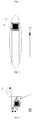
- a grounding soft board portion bonded with a shielding layer is generally strip-shaped (as shown by part A in FIG. 1 ).
- a windowing copper exposure region 11 is arranged inside a bonding region 10 at an end of the grounding soft board.
- the bonding area between the grounding soft board and the shielding layer is an area between the bonding region 10 and the windowing copper exposure region 11. Since the bonding area therebetween is small, the stressed points are relatively concentrated. Since this grounding soft board is strip-shaped, when stressed by an external force F (the stressed direction is indicated by an arrow), there is only one stressed direction and the stressed direction is in the body direction of the grounding soft board. Thus, the grounding soft board contacting the shielding layer is likely to fall off when folded and transported.
- a main objective of the present invention is to provide a flexible circuit board which can increase the bonding power.
- the present invention provides a flexible circuit board.
- the flexible circuit board includes a base portion and a grounding soft board extending from the base portion.
- the grounding soft board includes a board body connected to the base portion and a contact end arranged at a free end of the board body.
- the contact end includes a bonding region and a windowing copper exposure region arranged inside the bonding region.
- the board body is in a curved shape.
- the board body is S-shaped or W-shaped.
- the grounding soft board is configured to be contacted with a shielding layer of a touch screen, and a bonding area between the bonding region and the shielding layer is more than twice the bonding area between the windowing copper exposure region and the shielding region.
- the bonding region is L-shaped, T-shaped or cross-shaped.
- An anisotropic conducting adhesive film is coated on the bonding region and the windowing copper exposure region.
- the grounding soft board is prevented from falling off at portions contacting the shielding layer when folded or transported.
- the flexible circuit board of the present invention includes a base portion 1 and a grounding soft board B extending from the base portion 1.
- the grounding soft board B is configured to be contacted with a shielding layer of a touch screen.
- the grounding soft board B includes a board body 2 connected to the base portion 1 and a contact end arranged at a free end of the board body 2.
- the contact end includes a bonding region 20 and a windowing copper exposure region 21 arranged inside the bonding region 20.
- An anisotropic conducting adhesive film is coated on the bonding region 20 and the windowing copper exposure region 21.
- the bonding region 20 may be L-shaped.
- the bonding region 20 When compared with a square or rectangular bonding region, the bonding region 20 according to the present invention has a larger area.
- the area of the bonding between the grounding soft board B and the shielding layer may be increased such that the bonding area between the bonding region 20 and the shielding layer is more than twice the bonding area between the windowing copper exposure region 21 and the shielding layer. In this way, the bonding force of the grounding soft board B with the shielding layer is enhanced such that the grounding soft board B is prevented from falling off from the shielding layer when folded or transported.
- the bonding region 20 according to the present invention is not limited to an L-shape, and may also be in a T-shape, a cross-shape or other shapes which may increase the bonding area.
- the board body 2 of the grounding soft board B of the present invention is in a curved shape. As shown in FIG. 3 and FIG. 4 , the board body is S-shaped. When the grounding soft board is stressed by an actual external force Factual, this Factual is divided into folding stresses F1, F2, F3, F4 and F5 (as shown in FIG. 5 ) in various directions along the tangential direction of an edge of the board body 2, in order to weaken the force applied on a local portion of the board body 2. Thus, when the grounding soft board B of the present invention is stressed during folding or transportation, the bonding portion between the grounding soft board B and the shielding layer is less likely to fall off.
- the board body 2 of the grounding soft board B of the present invention is not limited to be an S-shape, and may be in a W-shape or other curved shapes.
- the grounding soft board is prevented from falling off at portions contacting the shielding layer when folded or transported.
Landscapes
- Engineering & Computer Science (AREA)
- Microelectronics & Electronic Packaging (AREA)
- General Engineering & Computer Science (AREA)
- Theoretical Computer Science (AREA)
- Human Computer Interaction (AREA)
- Physics & Mathematics (AREA)
- General Physics & Mathematics (AREA)
- Structure Of Printed Boards (AREA)
- Shielding Devices Or Components To Electric Or Magnetic Fields (AREA)
Applications Claiming Priority (2)
| Application Number | Priority Date | Filing Date | Title |
|---|---|---|---|
| CN201320879733.8U CN203775513U (zh) | 2013-12-30 | 2013-12-30 | 一种柔性电路板 |
| PCT/CN2014/095332 WO2015101256A1 (zh) | 2013-12-30 | 2014-12-29 | 一种柔性电路板 |
Publications (2)
| Publication Number | Publication Date |
|---|---|
| EP3071002A1 true EP3071002A1 (de) | 2016-09-21 |
| EP3071002A4 EP3071002A4 (de) | 2016-12-07 |
Family
ID=51292653
Family Applications (1)
| Application Number | Title | Priority Date | Filing Date |
|---|---|---|---|
| EP14876888.0A Withdrawn EP3071002A4 (de) | 2013-12-30 | 2014-12-29 | Flexible leiterplatte |
Country Status (7)
| Country | Link |
|---|---|
| US (1) | US20160330829A1 (de) |
| EP (1) | EP3071002A4 (de) |
| JP (1) | JP2017500759A (de) |
| KR (1) | KR20160099665A (de) |
| CN (1) | CN203775513U (de) |
| TW (1) | TWM499734U (de) |
| WO (1) | WO2015101256A1 (de) |
Families Citing this family (4)
| Publication number | Priority date | Publication date | Assignee | Title |
|---|---|---|---|---|
| CN203775513U (zh) * | 2013-12-30 | 2014-08-13 | 昆山维信诺显示技术有限公司 | 一种柔性电路板 |
| US10292268B2 (en) | 2015-12-24 | 2019-05-14 | Htc Corporation | Flexible printed circuit board, supporting holder and controller |
| CN206079072U (zh) * | 2016-10-17 | 2017-04-12 | 福州领头虎软件有限公司 | 一种带有电路板的服装 |
| CN106418758A (zh) * | 2016-10-17 | 2017-02-22 | 福州领头虎软件有限公司 | 一种带有电路板的服装 |
Family Cites Families (26)
| Publication number | Priority date | Publication date | Assignee | Title |
|---|---|---|---|---|
| US4040121A (en) * | 1975-05-27 | 1977-08-02 | Westinghouse Air Brake Company | Fail-safe printed circuit board connection |
| US5180888A (en) * | 1989-08-10 | 1993-01-19 | Casio Computer Co., Ltd. | Conductive bonding agent and a conductive connecting method |
| US5061830A (en) * | 1990-04-16 | 1991-10-29 | Ambrose Stephen D | Extension electrical switch system and method of manufacture |
| JPH09246682A (ja) * | 1996-03-13 | 1997-09-19 | Olympus Optical Co Ltd | プリント基板 |
| JPH11191662A (ja) * | 1997-12-25 | 1999-07-13 | Olympus Optical Co Ltd | フレキシブルプリント基板 |
| JP3501218B2 (ja) * | 2000-08-11 | 2004-03-02 | 日本電気株式会社 | フラットパネル表示モジュール及びその製造方法 |
| WO2002059969A1 (fr) * | 2001-01-23 | 2002-08-01 | Mitsubishi Denki Kabushiki Kaisha | Dispositif a semi-conducteur |
| TW543245B (en) * | 2002-05-17 | 2003-07-21 | Hon Hai Prec Ind Co Ltd | Electrical connector and method making the same |
| KR100442880B1 (ko) * | 2002-07-24 | 2004-08-02 | 삼성전자주식회사 | 적층형 반도체 모듈 및 그 제조방법 |
| JP2007165707A (ja) * | 2005-12-15 | 2007-06-28 | Nitto Denko Corp | フレキシブル配線回路基板 |
| US20080309633A1 (en) * | 2007-06-13 | 2008-12-18 | Apple Inc. | Touch-sensitive display |
| JP2009192976A (ja) * | 2008-02-18 | 2009-08-27 | Epson Imaging Devices Corp | 電気光学装置および電子機器 |
| US8456851B2 (en) * | 2008-05-16 | 2013-06-04 | Apple Inc. | Flex circuit with single sided routing and double sided attach |
| JP2010040888A (ja) * | 2008-08-07 | 2010-02-18 | Nec Saitama Ltd | フレキシブルプリント基板 |
| JP5185184B2 (ja) * | 2009-04-17 | 2013-04-17 | 株式会社ジャパンディスプレイセントラル | フレキシブルプリント基板およびその製造方法 |
| CN201550360U (zh) * | 2009-09-30 | 2010-08-11 | 华为终端有限公司 | 一种fpc接地耳朵 |
| JP5455034B2 (ja) * | 2009-12-09 | 2014-03-26 | ホシデン株式会社 | フレキシブル配線基板 |
| JP5370945B2 (ja) * | 2010-03-19 | 2013-12-18 | 株式会社ジャパンディスプレイ | タッチパネルおよび入力機能付き電気光学装置 |
| CN102316664B (zh) * | 2010-07-02 | 2013-08-28 | 富葵精密组件(深圳)有限公司 | 柔性电路板及其制作方法 |
| TWI476738B (zh) * | 2010-09-07 | 2015-03-11 | Ind Tech Res Inst | 軟性顯示面板及其組裝方法 |
| JP5665184B2 (ja) * | 2011-01-14 | 2015-02-04 | 株式会社小糸製作所 | 照明装置 |
| US9297972B2 (en) * | 2012-07-30 | 2016-03-29 | Glenair, Inc. | Advanced fiber-optic contact and method |
| CN203120284U (zh) * | 2013-02-05 | 2013-08-07 | 上海中航光电子有限公司 | 柔性线路板及液晶显示装置 |
| KR102042678B1 (ko) * | 2013-03-25 | 2019-11-11 | 삼성디스플레이 주식회사 | 디스플레이 장치 |
| US9545204B2 (en) * | 2013-09-25 | 2017-01-17 | Bardy Diagnostics, Inc. | Extended wear electrocardiography patch |
| CN203775513U (zh) * | 2013-12-30 | 2014-08-13 | 昆山维信诺显示技术有限公司 | 一种柔性电路板 |
-
2013
- 2013-12-30 CN CN201320879733.8U patent/CN203775513U/zh not_active Expired - Fee Related
-
2014
- 2014-12-29 EP EP14876888.0A patent/EP3071002A4/de not_active Withdrawn
- 2014-12-29 JP JP2016558255A patent/JP2017500759A/ja active Pending
- 2014-12-29 KR KR1020167019110A patent/KR20160099665A/ko not_active Ceased
- 2014-12-29 US US15/109,423 patent/US20160330829A1/en not_active Abandoned
- 2014-12-29 WO PCT/CN2014/095332 patent/WO2015101256A1/zh not_active Ceased
- 2014-12-30 TW TW103223275U patent/TWM499734U/zh not_active IP Right Cessation
Also Published As
| Publication number | Publication date |
|---|---|
| KR20160099665A (ko) | 2016-08-22 |
| TWM499734U (zh) | 2015-04-21 |
| EP3071002A4 (de) | 2016-12-07 |
| US20160330829A1 (en) | 2016-11-10 |
| JP2017500759A (ja) | 2017-01-05 |
| WO2015101256A1 (zh) | 2015-07-09 |
| CN203775513U (zh) | 2014-08-13 |
Similar Documents
| Publication | Publication Date | Title |
|---|---|---|
| US10440824B2 (en) | Flexible display device and electronic apparatus | |
| US11353939B2 (en) | Display panel | |
| US20160330829A1 (en) | Flexible printed circuit | |
| US11882751B2 (en) | Display device and method for manufacturing the same | |
| CN205566782U (zh) | 柔性电路板 | |
| US10531559B2 (en) | Electronic device | |
| JP5718862B2 (ja) | プリント配線板上保護フィルムの剥離治具 | |
| US20240213181A1 (en) | Display panel and display device | |
| CN104991369A (zh) | 显示模组及显示装置 | |
| CN104582249B (zh) | 一种柔性印刷线路板组件及其电子设备 | |
| US10973121B2 (en) | Backlight golden finger structure and display device | |
| CN209561656U (zh) | Ffc排线 | |
| JP2017022225A (ja) | 基板及び電子機器 | |
| CN204859740U (zh) | 柔性电路板 | |
| US9426934B2 (en) | Shield case and electronic apparatus | |
| CN115380631B (zh) | 电路板模组 | |
| CN112020207B (zh) | 柔性印刷电路板及显示装置 | |
| CN222283557U (zh) | 一种背板组件、背光模组和显示装置 | |
| CN105528123A (zh) | 触控组件及其制作方法 | |
| CN205648187U (zh) | 显示装置及其保护片结构 | |
| WO2014203753A1 (ja) | フレキシブル基板及びこれを具えた電子機器 | |
| CN218951314U (zh) | 一种不会造成Metal Mesh失效的保护膜 | |
| US20180354224A1 (en) | Flexible laminated structure and display | |
| CN104335363B (zh) | 电子设备及电子设备的制造方法 | |
| CN101657086A (zh) | 防电磁辐射装置 |
Legal Events
| Date | Code | Title | Description |
|---|---|---|---|
| PUAI | Public reference made under article 153(3) epc to a published international application that has entered the european phase |
Free format text: ORIGINAL CODE: 0009012 |
|
| 17P | Request for examination filed |
Effective date: 20160615 |
|
| AK | Designated contracting states |
Kind code of ref document: A1 Designated state(s): AL AT BE BG CH CY CZ DE DK EE ES FI FR GB GR HR HU IE IS IT LI LT LU LV MC MK MT NL NO PL PT RO RS SE SI SK SM TR |
|
| AX | Request for extension of the european patent |
Extension state: BA ME |
|
| A4 | Supplementary search report drawn up and despatched |
Effective date: 20161109 |
|
| RIC1 | Information provided on ipc code assigned before grant |
Ipc: H05K 1/02 20060101AFI20161103BHEP |
|
| DAX | Request for extension of the european patent (deleted) | ||
| STAA | Information on the status of an ep patent application or granted ep patent |
Free format text: STATUS: THE APPLICATION HAS BEEN WITHDRAWN |
|
| 18W | Application withdrawn |
Effective date: 20170520 |