EP3075737B1 - Benzimidazolo [1,2-a] benzimidazole portant des groupes heteroarylnitril aryl- ou pour diodes électroluminescentes organiques - Google Patents
Benzimidazolo [1,2-a] benzimidazole portant des groupes heteroarylnitril aryl- ou pour diodes électroluminescentes organiques Download PDFInfo
- Publication number
- EP3075737B1 EP3075737B1 EP15161950.9A EP15161950A EP3075737B1 EP 3075737 B1 EP3075737 B1 EP 3075737B1 EP 15161950 A EP15161950 A EP 15161950A EP 3075737 B1 EP3075737 B1 EP 3075737B1
- Authority
- EP
- European Patent Office
- Prior art keywords
- compounds
- formula
- group
- layer
- compound
- Prior art date
- Legal status (The legal status is an assumption and is not a legal conclusion. Google has not performed a legal analysis and makes no representation as to the accuracy of the status listed.)
- Active
Links
- 0 *NC([n]1c2nc3ccccc3[n]2c2c1cccc2)=N* Chemical compound *NC([n]1c2nc3ccccc3[n]2c2c1cccc2)=N* 0.000 description 18
- SDFLTYHTFPTIGX-UHFFFAOYSA-N C[n]1c(cccc2)c2c2c1cccc2 Chemical compound C[n]1c(cccc2)c2c2c1cccc2 SDFLTYHTFPTIGX-UHFFFAOYSA-N 0.000 description 2
- UWDTYENJIOEORT-UHFFFAOYSA-N C[n]1c2nc3ccccc3[n]2c2c1cccc2 Chemical compound C[n]1c2nc3ccccc3[n]2c2c1cccc2 UWDTYENJIOEORT-UHFFFAOYSA-N 0.000 description 2
- RIHYWDOIYSYQGU-UHFFFAOYSA-N N#Cc1cc(-[n]2c3nc(cccc4)c4[n]3c3cc(I)ccc23)ccc1 Chemical compound N#Cc1cc(-[n]2c3nc(cccc4)c4[n]3c3cc(I)ccc23)ccc1 RIHYWDOIYSYQGU-UHFFFAOYSA-N 0.000 description 2
- KLACMEYLRXQSMN-UHFFFAOYSA-N c(cc1[nH]2)ccc1[n]1c2nc2c1cccc2 Chemical compound c(cc1[nH]2)ccc1[n]1c2nc2c1cccc2 KLACMEYLRXQSMN-UHFFFAOYSA-N 0.000 description 2
- VPKIVADTTRODQQ-UHFFFAOYSA-N C(C1)C=Cc(c2c3cccc2)c1[n]3-c(cc1c2ccccc22)ccc1[n]2-c1cc([Si](C(C2)=CC=CC2c2c3[s]c(cccc4)c4c3ccc2)(c2ccccc2)c2ccccc2)ccc1 Chemical compound C(C1)C=Cc(c2c3cccc2)c1[n]3-c(cc1c2ccccc22)ccc1[n]2-c1cc([Si](C(C2)=CC=CC2c2c3[s]c(cccc4)c4c3ccc2)(c2ccccc2)c2ccccc2)ccc1 VPKIVADTTRODQQ-UHFFFAOYSA-N 0.000 description 1
- NPLIJEDZUGESDD-MUADHRSZSA-N C=NCc(c(-[n]1c2nc(cccc3)c3[n]2c2c1C1C=CC=C[C@@H]21)ccc1)c1-c1ccc2[o]c(ccc(-[n]3c(cccc4)c4c4c3cccc4)c3)c3c2c1 Chemical compound C=NCc(c(-[n]1c2nc(cccc3)c3[n]2c2c1C1C=CC=C[C@@H]21)ccc1)c1-c1ccc2[o]c(ccc(-[n]3c(cccc4)c4c4c3cccc4)c3)c3c2c1 NPLIJEDZUGESDD-MUADHRSZSA-N 0.000 description 1
- WGBSRLVEOCQZST-UHFFFAOYSA-O CC(C(C#N)=C(C=C)N1C2=Nc3ccccc3[NH+]2c2c1cccc2)[n]1c2nc3ccccc3[n]2c2ccccc12 Chemical compound CC(C(C#N)=C(C=C)N1C2=Nc3ccccc3[NH+]2c2c1cccc2)[n]1c2nc3ccccc3[n]2c2ccccc12 WGBSRLVEOCQZST-UHFFFAOYSA-O 0.000 description 1
- WAAFSLSDPBHQOK-UHFFFAOYSA-N CC(C)C1=CC=CC1C Chemical compound CC(C)C1=CC=CC1C WAAFSLSDPBHQOK-UHFFFAOYSA-N 0.000 description 1
- ROFIQODOBRAUSO-UHFFFAOYSA-N CC(N(C)C=C1)N1c1c(C)ccc2c1[o]c1ccccc21 Chemical compound CC(N(C)C=C1)N1c1c(C)ccc2c1[o]c1ccccc21 ROFIQODOBRAUSO-UHFFFAOYSA-N 0.000 description 1
- ZBIKORITPGTTGI-UHFFFAOYSA-N CC(O[I](c1ccccc1)OC(C)=O)=O Chemical compound CC(O[I](c1ccccc1)OC(C)=O)=O ZBIKORITPGTTGI-UHFFFAOYSA-N 0.000 description 1
- ORWRFLSTLDPQJS-UHFFFAOYSA-N CC1C(C)=CC=C1 Chemical compound CC1C(C)=CC=C1 ORWRFLSTLDPQJS-UHFFFAOYSA-N 0.000 description 1
- HSXQTOBKWYXKMU-UHFFFAOYSA-N CCC(C)(C12)C(CC)(CC)c(cccc3)c3N1c1nc(CC)c(CC)nc1N2c1ccccc1 Chemical compound CCC(C)(C12)C(CC)(CC)c(cccc3)c3N1c1nc(CC)c(CC)nc1N2c1ccccc1 HSXQTOBKWYXKMU-UHFFFAOYSA-N 0.000 description 1
- XPBUOEXLBLYLCA-UHFFFAOYSA-N C[SiH](c(cc1)cc2c1[o]c(cc1)c2cc1-[n]1c(cccc2)c2c2c1cccc2)c(cc1)cc(c2c3)c1[o]c2ccc3-[n]1c2ccccc2c2c1cccc2 Chemical compound C[SiH](c(cc1)cc2c1[o]c(cc1)c2cc1-[n]1c(cccc2)c2c2c1cccc2)c(cc1)cc(c2c3)c1[o]c2ccc3-[n]1c2ccccc2c2c1cccc2 XPBUOEXLBLYLCA-UHFFFAOYSA-N 0.000 description 1
- HVTIOHAXYSBZLK-UHFFFAOYSA-N C[n]1c(ccc(-[n]2c3nc(cccc4)c4[n]3c3ccccc23)c2)c2c2c1cccc2 Chemical compound C[n]1c(ccc(-[n]2c3nc(cccc4)c4[n]3c3ccccc23)c2)c2c2c1cccc2 HVTIOHAXYSBZLK-UHFFFAOYSA-N 0.000 description 1
- LDTOAZMVWNUPCO-UHFFFAOYSA-N C[n]1c2nc(cccc3)c3[n]2c2cc(-[n]3c(cccc4)c4c4c3cccc4)ccc12 Chemical compound C[n]1c2nc(cccc3)c3[n]2c2cc(-[n]3c(cccc4)c4c4c3cccc4)ccc12 LDTOAZMVWNUPCO-UHFFFAOYSA-N 0.000 description 1
- MQDRPHOWOQNMJE-UHFFFAOYSA-N Cc(c(C)c1)cc2c1nc1[n]2c2ccccc2[nH]1 Chemical compound Cc(c(C)c1)cc2c1nc1[n]2c2ccccc2[nH]1 MQDRPHOWOQNMJE-UHFFFAOYSA-N 0.000 description 1
- CHLICZRVGGXEOD-UHFFFAOYSA-N Cc(cc1)ccc1OC Chemical compound Cc(cc1)ccc1OC CHLICZRVGGXEOD-UHFFFAOYSA-N 0.000 description 1
- AUHZEENZYGFFBQ-UHFFFAOYSA-N Cc1cc(C)cc(C)c1 Chemical compound Cc1cc(C)cc(C)c1 AUHZEENZYGFFBQ-UHFFFAOYSA-N 0.000 description 1
- URLKBWYHVLBVBO-UHFFFAOYSA-N Cc1ccc(C)cc1 Chemical compound Cc1ccc(C)cc1 URLKBWYHVLBVBO-UHFFFAOYSA-N 0.000 description 1
- LHHWHFDZFRUYFD-UHFFFAOYSA-N N#Cc(c(-[n]1c2nc3ccccc3[n]2c2c1cccc2)ccc1-[n]2c3nc(cccc4)c4[n]3c3ccccc23)c1-[n]1c2nc(cccc3)c3[n]2c2c1cccc2 Chemical compound N#Cc(c(-[n]1c2nc3ccccc3[n]2c2c1cccc2)ccc1-[n]2c3nc(cccc4)c4[n]3c3ccccc23)c1-[n]1c2nc(cccc3)c3[n]2c2c1cccc2 LHHWHFDZFRUYFD-UHFFFAOYSA-N 0.000 description 1
- YWTXHALVWAISPR-UHFFFAOYSA-N N#Cc(c(F)c(cc1)F)c1F Chemical compound N#Cc(c(F)c(cc1)F)c1F YWTXHALVWAISPR-UHFFFAOYSA-N 0.000 description 1
- LQPBDSQNDZYFHX-UHFFFAOYSA-N N#Cc(cccc1-[n]2c3nc(cccc4)c4[n]3c3ccccc23)c1C#N Chemical compound N#Cc(cccc1-[n]2c3nc(cccc4)c4[n]3c3ccccc23)c1C#N LQPBDSQNDZYFHX-UHFFFAOYSA-N 0.000 description 1
- WWZRHCWWNKVYIA-UHFFFAOYSA-N N#Cc(cccc1-c(cc2)cc(c3c4)c2[o]c3ccc4-[n]2c3ccccc3c3c2cccc3)c1-[n]1c2nc(cccc3)c3[n]2c2c1cccc2 Chemical compound N#Cc(cccc1-c(cc2)cc(c3c4)c2[o]c3ccc4-[n]2c3ccccc3c3c2cccc3)c1-[n]1c2nc(cccc3)c3[n]2c2c1cccc2 WWZRHCWWNKVYIA-UHFFFAOYSA-N 0.000 description 1
- DBGQFLFGWUYOOQ-UHFFFAOYSA-N N#Cc1cc(-[n]2c3nc(cccc4)c4[n]3c3c2cccc3)ccc1 Chemical compound N#Cc1cc(-[n]2c3nc(cccc4)c4[n]3c3c2cccc3)ccc1 DBGQFLFGWUYOOQ-UHFFFAOYSA-N 0.000 description 1
- WIAVVLDQXGSYMV-UHFFFAOYSA-N N#Cc1cc(-[n]2c3nc(cccc4)c4[n]3c3cc([Si+](c4ccccc4)(c4ccccc4)c4ccccc4)ccc23)ccc1 Chemical compound N#Cc1cc(-[n]2c3nc(cccc4)c4[n]3c3cc([Si+](c4ccccc4)(c4ccccc4)c4ccccc4)ccc23)ccc1 WIAVVLDQXGSYMV-UHFFFAOYSA-N 0.000 description 1
- UFHAMNUEKASFQD-UHFFFAOYSA-N N#Cc1cc(-[n]2c3nc(cccc4)c4[n]3c3ccccc23)cc(C#N)c1 Chemical compound N#Cc1cc(-[n]2c3nc(cccc4)c4[n]3c3ccccc23)cc(C#N)c1 UFHAMNUEKASFQD-UHFFFAOYSA-N 0.000 description 1
- FTKGPLRXOBGESD-UHFFFAOYSA-N N#Cc1cccc(-[n]2c3nc(cccc4)c4[n]3c3c2cccc3)c1-[n]1c2nc(cccc3)c3[n]2c2c1cccc2 Chemical compound N#Cc1cccc(-[n]2c3nc(cccc4)c4[n]3c3c2cccc3)c1-[n]1c2nc(cccc3)c3[n]2c2c1cccc2 FTKGPLRXOBGESD-UHFFFAOYSA-N 0.000 description 1
- JAQFYXLPLCLPCX-UHFFFAOYSA-N N#Cc1cccc(C#N)c1-[n]1c2nc3ccccc3[n]2c2c1cccc2 Chemical compound N#Cc1cccc(C#N)c1-[n]1c2nc3ccccc3[n]2c2c1cccc2 JAQFYXLPLCLPCX-UHFFFAOYSA-N 0.000 description 1
- QXRFMGPPJWEBIX-UHFFFAOYSA-N c(cc1)ccc1-[n](c1ccccc1c1c2)c1ccc2-c(cc1)cc(c2c3cccc2)c1[n]3-c1c2[s]c(cccc3)c3c2ccn1 Chemical compound c(cc1)ccc1-[n](c1ccccc1c1c2)c1ccc2-c(cc1)cc(c2c3cccc2)c1[n]3-c1c2[s]c(cccc3)c3c2ccn1 QXRFMGPPJWEBIX-UHFFFAOYSA-N 0.000 description 1
- LIABTNDKTKNVCF-UHFFFAOYSA-N c(cc1)ccc1-c1nc(-[n]2c3nc4ccccc4[n]3c3c2cccc3)nc(-c2ccccc2)n1 Chemical compound c(cc1)ccc1-c1nc(-[n]2c3nc4ccccc4[n]3c3c2cccc3)nc(-c2ccccc2)n1 LIABTNDKTKNVCF-UHFFFAOYSA-N 0.000 description 1
- WCXKTQVEKDHQIY-UHFFFAOYSA-N c1cc(-c2cc(-c3cnccc3)cc(-c3cccnc3)c2)cc(-c2cc(-c3cnccc3)cc(-c3cccnc3)c2)c1 Chemical compound c1cc(-c2cc(-c3cnccc3)cc(-c3cccnc3)c2)cc(-c2cc(-c3cnccc3)cc(-c3cccnc3)c2)c1 WCXKTQVEKDHQIY-UHFFFAOYSA-N 0.000 description 1
- LTEREIPNJSCEHH-UHFFFAOYSA-N c1cc(cc2)c3c4c2ccc(-c(cc2)cc(c5c6)c2[o]c5ccc6-c2c(ccc5cccc(cc6)c55)c5c6cc2)c4ccc3c1 Chemical compound c1cc(cc2)c3c4c2ccc(-c(cc2)cc(c5c6)c2[o]c5ccc6-c2c(ccc5cccc(cc6)c55)c5c6cc2)c4ccc3c1 LTEREIPNJSCEHH-UHFFFAOYSA-N 0.000 description 1
Classifications
-
- C—CHEMISTRY; METALLURGY
- C07—ORGANIC CHEMISTRY
- C07D—HETEROCYCLIC COMPOUNDS
- C07D487/00—Heterocyclic compounds containing nitrogen atoms as the only ring hetero atoms in the condensed system, not provided for by groups C07D451/00 - C07D477/00
- C07D487/02—Heterocyclic compounds containing nitrogen atoms as the only ring hetero atoms in the condensed system, not provided for by groups C07D451/00 - C07D477/00 in which the condensed system contains two hetero rings
- C07D487/04—Ortho-condensed systems
-
- C—CHEMISTRY; METALLURGY
- C09—DYES; PAINTS; POLISHES; NATURAL RESINS; ADHESIVES; COMPOSITIONS NOT OTHERWISE PROVIDED FOR; APPLICATIONS OF MATERIALS NOT OTHERWISE PROVIDED FOR
- C09K—MATERIALS FOR MISCELLANEOUS APPLICATIONS, NOT PROVIDED FOR ELSEWHERE
- C09K11/00—Luminescent materials, e.g. electroluminescent or chemiluminescent
- C09K11/06—Luminescent materials, e.g. electroluminescent or chemiluminescent containing organic luminescent materials
-
- H—ELECTRICITY
- H10—SEMICONDUCTOR DEVICES; ELECTRIC SOLID-STATE DEVICES NOT OTHERWISE PROVIDED FOR
- H10K—ORGANIC ELECTRIC SOLID-STATE DEVICES
- H10K50/00—Organic light-emitting devices
- H10K50/10—OLEDs or polymer light-emitting diodes [PLED]
- H10K50/11—OLEDs or polymer light-emitting diodes [PLED] characterised by the electroluminescent [EL] layers
-
- H—ELECTRICITY
- H10—SEMICONDUCTOR DEVICES; ELECTRIC SOLID-STATE DEVICES NOT OTHERWISE PROVIDED FOR
- H10K—ORGANIC ELECTRIC SOLID-STATE DEVICES
- H10K85/00—Organic materials used in the body or electrodes of devices covered by this subclass
- H10K85/60—Organic compounds having low molecular weight
- H10K85/649—Aromatic compounds comprising a hetero atom
- H10K85/657—Polycyclic condensed heteroaromatic hydrocarbons
- H10K85/6572—Polycyclic condensed heteroaromatic hydrocarbons comprising only nitrogen in the heteroaromatic polycondensed ring system, e.g. phenanthroline or carbazole
-
- C—CHEMISTRY; METALLURGY
- C09—DYES; PAINTS; POLISHES; NATURAL RESINS; ADHESIVES; COMPOSITIONS NOT OTHERWISE PROVIDED FOR; APPLICATIONS OF MATERIALS NOT OTHERWISE PROVIDED FOR
- C09K—MATERIALS FOR MISCELLANEOUS APPLICATIONS, NOT PROVIDED FOR ELSEWHERE
- C09K2211/00—Chemical nature of organic luminescent or tenebrescent compounds
- C09K2211/10—Non-macromolecular compounds
- C09K2211/1018—Heterocyclic compounds
- C09K2211/1025—Heterocyclic compounds characterised by ligands
- C09K2211/1029—Heterocyclic compounds characterised by ligands containing one nitrogen atom as the heteroatom
-
- C—CHEMISTRY; METALLURGY
- C09—DYES; PAINTS; POLISHES; NATURAL RESINS; ADHESIVES; COMPOSITIONS NOT OTHERWISE PROVIDED FOR; APPLICATIONS OF MATERIALS NOT OTHERWISE PROVIDED FOR
- C09K—MATERIALS FOR MISCELLANEOUS APPLICATIONS, NOT PROVIDED FOR ELSEWHERE
- C09K2211/00—Chemical nature of organic luminescent or tenebrescent compounds
- C09K2211/10—Non-macromolecular compounds
- C09K2211/1018—Heterocyclic compounds
- C09K2211/1025—Heterocyclic compounds characterised by ligands
- C09K2211/1059—Heterocyclic compounds characterised by ligands containing three nitrogen atoms as heteroatoms
-
- C—CHEMISTRY; METALLURGY
- C09—DYES; PAINTS; POLISHES; NATURAL RESINS; ADHESIVES; COMPOSITIONS NOT OTHERWISE PROVIDED FOR; APPLICATIONS OF MATERIALS NOT OTHERWISE PROVIDED FOR
- C09K—MATERIALS FOR MISCELLANEOUS APPLICATIONS, NOT PROVIDED FOR ELSEWHERE
- C09K2211/00—Chemical nature of organic luminescent or tenebrescent compounds
- C09K2211/10—Non-macromolecular compounds
- C09K2211/1018—Heterocyclic compounds
- C09K2211/1025—Heterocyclic compounds characterised by ligands
- C09K2211/1088—Heterocyclic compounds characterised by ligands containing oxygen as the only heteroatom
-
- C—CHEMISTRY; METALLURGY
- C09—DYES; PAINTS; POLISHES; NATURAL RESINS; ADHESIVES; COMPOSITIONS NOT OTHERWISE PROVIDED FOR; APPLICATIONS OF MATERIALS NOT OTHERWISE PROVIDED FOR
- C09K—MATERIALS FOR MISCELLANEOUS APPLICATIONS, NOT PROVIDED FOR ELSEWHERE
- C09K2211/00—Chemical nature of organic luminescent or tenebrescent compounds
- C09K2211/10—Non-macromolecular compounds
- C09K2211/1018—Heterocyclic compounds
- C09K2211/1025—Heterocyclic compounds characterised by ligands
- C09K2211/1092—Heterocyclic compounds characterised by ligands containing sulfur as the only heteroatom
-
- H—ELECTRICITY
- H10—SEMICONDUCTOR DEVICES; ELECTRIC SOLID-STATE DEVICES NOT OTHERWISE PROVIDED FOR
- H10K—ORGANIC ELECTRIC SOLID-STATE DEVICES
- H10K2101/00—Properties of the organic materials covered by group H10K85/00
- H10K2101/10—Triplet emission
-
- H—ELECTRICITY
- H10—SEMICONDUCTOR DEVICES; ELECTRIC SOLID-STATE DEVICES NOT OTHERWISE PROVIDED FOR
- H10K—ORGANIC ELECTRIC SOLID-STATE DEVICES
- H10K50/00—Organic light-emitting devices
- H10K50/10—OLEDs or polymer light-emitting diodes [PLED]
- H10K50/14—Carrier transporting layers
- H10K50/16—Electron transporting layers
- H10K50/165—Electron transporting layers comprising dopants
-
- H—ELECTRICITY
- H10—SEMICONDUCTOR DEVICES; ELECTRIC SOLID-STATE DEVICES NOT OTHERWISE PROVIDED FOR
- H10K—ORGANIC ELECTRIC SOLID-STATE DEVICES
- H10K50/00—Organic light-emitting devices
- H10K50/10—OLEDs or polymer light-emitting diodes [PLED]
- H10K50/18—Carrier blocking layers
-
- H—ELECTRICITY
- H10—SEMICONDUCTOR DEVICES; ELECTRIC SOLID-STATE DEVICES NOT OTHERWISE PROVIDED FOR
- H10K—ORGANIC ELECTRIC SOLID-STATE DEVICES
- H10K85/00—Organic materials used in the body or electrodes of devices covered by this subclass
- H10K85/30—Coordination compounds
- H10K85/341—Transition metal complexes, e.g. Ru(II)polypyridine complexes
- H10K85/342—Transition metal complexes, e.g. Ru(II)polypyridine complexes comprising iridium
-
- H—ELECTRICITY
- H10—SEMICONDUCTOR DEVICES; ELECTRIC SOLID-STATE DEVICES NOT OTHERWISE PROVIDED FOR
- H10K—ORGANIC ELECTRIC SOLID-STATE DEVICES
- H10K85/00—Organic materials used in the body or electrodes of devices covered by this subclass
- H10K85/40—Organosilicon compounds, e.g. TIPS pentacene
-
- H—ELECTRICITY
- H10—SEMICONDUCTOR DEVICES; ELECTRIC SOLID-STATE DEVICES NOT OTHERWISE PROVIDED FOR
- H10K—ORGANIC ELECTRIC SOLID-STATE DEVICES
- H10K85/00—Organic materials used in the body or electrodes of devices covered by this subclass
- H10K85/60—Organic compounds having low molecular weight
- H10K85/649—Aromatic compounds comprising a hetero atom
- H10K85/657—Polycyclic condensed heteroaromatic hydrocarbons
- H10K85/6574—Polycyclic condensed heteroaromatic hydrocarbons comprising only oxygen in the heteroaromatic polycondensed ring system, e.g. cumarine dyes
-
- H—ELECTRICITY
- H10—SEMICONDUCTOR DEVICES; ELECTRIC SOLID-STATE DEVICES NOT OTHERWISE PROVIDED FOR
- H10K—ORGANIC ELECTRIC SOLID-STATE DEVICES
- H10K85/00—Organic materials used in the body or electrodes of devices covered by this subclass
- H10K85/60—Organic compounds having low molecular weight
- H10K85/649—Aromatic compounds comprising a hetero atom
- H10K85/657—Polycyclic condensed heteroaromatic hydrocarbons
- H10K85/6576—Polycyclic condensed heteroaromatic hydrocarbons comprising only sulfur in the heteroaromatic polycondensed ring system, e.g. benzothiophene
-
- Y—GENERAL TAGGING OF NEW TECHNOLOGICAL DEVELOPMENTS; GENERAL TAGGING OF CROSS-SECTIONAL TECHNOLOGIES SPANNING OVER SEVERAL SECTIONS OF THE IPC; TECHNICAL SUBJECTS COVERED BY FORMER USPC CROSS-REFERENCE ART COLLECTIONS [XRACs] AND DIGESTS
- Y02—TECHNOLOGIES OR APPLICATIONS FOR MITIGATION OR ADAPTATION AGAINST CLIMATE CHANGE
- Y02E—REDUCTION OF GREENHOUSE GAS [GHG] EMISSIONS, RELATED TO ENERGY GENERATION, TRANSMISSION OR DISTRIBUTION
- Y02E10/00—Energy generation through renewable energy sources
- Y02E10/50—Photovoltaic [PV] energy
- Y02E10/549—Organic PV cells
Definitions
- the present invention relates to compounds of formula Ib and their use in electronic devices, especially electroluminescent devices.
- the compounds of formula Ib When used as charge transport material, charge blocker material and/or host material in electroluminescent devices, the compounds of formula Ib may provide improved efficiency, stability, manufacturability, or spectral characteristics of electroluminescent devices and reduced driving voltage of electroluminescent devices.
- said compounds of formula Ib show low singlet triplet splitting, which makes them useful as TADF ( Thermally Activated Delayed Fluorescence, Adv. Mater. 2014, 26, 7931-7958 ) emitter or TADF host materials in combination with fluorescent emitters.
- TADF Thermally Activated Delayed Fluorescence, Adv. Mater. 2014, 26, 7931-7958
- WO2011/160757 relates to an electronic device comprising an anode, cathode and at least one organic layer which contains a compound of formulae wherein X may be a single bond and L may be a divalent group.
- X may be a single bond
- L may be a divalent group.
- WO2012/130709 relates to 4H-Imidazo[1,2-a]imidazoles, such as , for example, (A-1), a process for their production and their use in electronic devices, especially electroluminescent devices.
- WO2014/009317 relates to compounds of formula especially compounds of formula such as, for example, and a process for their production and their use in electronic devices, especially electroluminescent devices.
- the 2,5-disubstituted benzimidazo[1,2-a]benzimidazole derivatives are suitable hole transporting materials, or host materials for phosphorescent emitters.
- WO2014/044722 relates to compounds of formula which are characterized in that they substituted by benzimidazo[1,2-a]benzimidazo-5-yl and/or benzimidazo[1,2-a]benzimidazo-2,5-ylene groups and in that at least one of the substituents B 1 , B 2 , B 3 , B 4 , B 5 , B 6 , B 7 and B 8 represents N, a process for their production and their use in electronic devices, especially electroluminescent devices.
- European patent application no. 13191100.0 relates to compounds of formula which are characterized in that they are substituted by benzimidazo[1,2-a]benzimidazo-5-yl and/or benzimidazo[1,2-a]benzimidazo-2,5-ylene groups and in that at least one of the substituents B 1 , B 2 , B 3 , B 4 , B 5 , B 6 , B 7 and B 8 represents N; a process for their production and their use in electronic devices, especially electroluminescent devices.
- European patent application no. 14162667.1 relates to compounds of the formula especially wherein X 1 is H, a group of formula X 7 and X 3 are independently of each other H, or a group of formula or wherein at least one of X 1 , X 2 and X 3 is a group of formula or comprises a group of formula
- Benzimidazo[1,2-a]benzimidazo-5-yl and benzimidazo[1,2-a]benzimidazo-2-ylsubstituted benzimidazolo[2,1-b][1,3]benzothiazole derivatives are described in PCT/EP2014/066174 .
- Azabenzimidazo[2,1-a]benzimidazoles for electronic applications are described in European patent application no. 14183598.3 .
- EP14197947.9 describes carbazol compounds carrying benzimidazolo[1,2-a]benzimidazole groups of the following structure.
- EP14193401.8 describes nitril-indolo compounds carrying benzimidazolo[1,2-a]benzimidazole groups. The following compound is described:
- EP14197952.6 describes dibenzofurane compounds carrying benzimidazolo[1,2-a]benzimidazole groups of the following structure.
- WO2013/154064 A1 discloses an organic light emitting element, which has a comopound of the following formula in the light emitting layer: wherein at least one of R 1 to R 5 represents a cyano group, at least one of R 1 to R 5 represents a 9-carbazolyl group, a 1,2,3,4-terahydro-9-carbazolyl group, a 1-indolyl group or a diarylamino group, and the rest of R 1 to R 5 represent a hydrogen atom or a substituent.
- EP 2 039 737 A2 concerns an organic electroluminescence device comprising a compound of formula (I) wherein a represents an aromatic ring which may have a substituent, m represents an integer of 2 or greater, and n represents an integer of 1 or greater.
- WO2013/154064 A1 nor EP 2 039 737 A2 disclose compounds comprising benzimidazolo[1,2-a]benzimidazole groups.
- US 2014/0001446 A1 relates to a material for organic EL devices represented by formula (I)
- the material for organic EL devices represented by formula (I) has a central skeleton to which a cyano-substituted aromatic hydrocarbon group or a cyano-substituted heterocyclic group is bonded at a specific position.
- materials showing low singlet triplet splitting which makes them useful as TADF ( Thermally Activated Delayed Fluorescence, Adv. Mater. 2014, 26, 7931-7958 ) emitter or TADF host materials in combination with fluorescent emitters.
- the materials should be suitable especially for OLEDs which comprise at least one emitter, which is preferably a phosphorescence emitter, especially at least one green emitter or at least one blue emitter. It should further be possible to provide materials showing low singlet triplet splitting, which makes them useful as TADF ( Thermally Activated Delayed Fluorescence, Adv. Mater. 2014, 26, 7931-7958 ) emitter or TADF host materials in combination with fluorescent emitters.
- TADF Thermally Activated Delayed Fluorescence, Adv. Mater. 2014, 26, 7931-7958
- the materials should be suitable for providing OLEDs which ensure good efficiencies, good operative lifetimes and a high stability to thermal stress, and a low use and operating voltage of the OLEDs.
- the compounds of the present invention are characterized by a high acceptor strength, efficient bipolar characteristics and a good suitability as TADF hosts or emitters.
- the compounds of the present invention may be used for electrophotographic photoreceptors, photoelectric converters, organic solar cells (organic photovoltaics), switching elements, such as organic transistors, for example, organic FETs and organic TFTs, organic light emitting field effect transistors (OLEFETs), image sensors, dye lasers and electroluminescent devices, such as, for example, organic light-emitting diodes (OLEDs).
- organic photoreceptors organic solar cells
- organic photovoltaics organic solar cells
- switching elements such as organic transistors, for example, organic FETs and organic TFTs, organic light emitting field effect transistors (OLEFETs), image sensors, dye lasers and electroluminescent devices, such as, for example, organic light-emitting diodes (OLEDs).
- a further subject of the present invention is directed to an electronic device, comprising a compound according to the present invention.
- the electronic device is preferably an electroluminescent device, such as an organic light-emitting diode (OLED).
- OLED organic light-emitting diode
- the compounds of formula Ib can in principal be used in any layer of an EL device, but are preferably used as host, charge transport and/or charge/exciton blocking material. Particularly, the compounds of formula Ib are used as host material for green, especially blue light emitting phosphorescent emitters. Additionally, the compounds of formula Ib are used as TADF emitter or TADF host materials in combination with at least one fluorescent emitter, especially in OLEDs emitting in the blue and green region of the electromagnetic spectrum.
- a further subject of the present invention is directed to a charge transport layer, comprising a compound of formula Ib according to the present invention.
- a further subject of the present invention is directed to an emitting layer, comprising a compound of formula Ib according to the present invention.
- a compound of formula Ib is preferably used as host material, more preferably in combination with a phosphorescent emitter.
- a further subject of the present invention is directed to a charge/exciton blocking layer, comprising a compound of formula Ib according to the present invention.
- a further subject of the present invention is directed to an OLED comprising at least one compound of formula Ib as TADF emitter or TADF host material in combination with at least one fluorescent emitter.
- halogen alkyl, alkoxy, cycloalkyl, aryl, aryloxy, aralkyl, heteroaryl, arylene, heteroarylene generally have the following meaning, if said groups are not further specified in specific embodiments mentioned below:
- Halogen is fluorine, chlorine, bromine and iodine.
- C 1 -C 25 alkyl (C 1 -C 18 alkyl) is typically linear or branched, where possible. Examples are methyl, ethyl, n-propyl, isopropyl, n-butyl, sec.-butyl, isobutyl, tert.-butyl, n-pentyl, 2-pentyl, 3-pentyl, 2,2-dimethylpropyl, 1,1,3,3-tetramethylpentyl, n-hexyl, 1-methylhexyl, 1,1,3,3,5,5-hexamethylhexyl, n-heptyl, isoheptyl, 1,1,3,3-tetramethylbutyl, 1-methylheptyl, 3-methylheptyl, n-octyl, 1,1,3,3-tetramethylbutyl and 2-ethylhexyl, n-nonyl, decyl, undecyl, dodecy
- C 1 -C 8 alkyl is typically methyl, ethyl, n-propyl, isopropyl, n-butyl, sec.-butyl, isobutyl, tert.-butyl, n-pentyl, 2-pentyl, 3-pentyl, 2,2-dimethyl-propyl, n-hexyl, n-heptyl, n-octyl, 1,1,3,3-tetramethylbutyl and 2-ethylhexyl.
- C 1 -C 4 alkyl is typically methyl, ethyl, n-propyl, isopropyl, n-butyl, sec.-butyl, isobutyl, tert.-butyl.
- C 1 -C 25 alkoxy groups are straight-chain or branched alkoxy groups, e.g. methoxy, ethoxy, n-propoxy, isopropoxy, n-butoxy, sec-butoxy, tert-butoxy, amyloxy, isoamyloxy or tert-amyloxy, heptyloxy, octyloxy, isooctyloxy, nonyloxy, decyloxy, undecyloxy, dodecyloxy, tetradecyloxy, pentadecyloxy, hexadecyloxy, heptadecyloxy and octadecyloxy.
- C 1 -C 8 alkoxy examples are methoxy, ethoxy, n-propoxy, isopropoxy, n-butoxy, sec.-butoxy, isobutoxy, tert.-butoxy, n-pentyloxy, 2-pentyloxy, 3-pentyloxy, 2,2-dimethylpropoxy, n-hexyloxy, n-heptyloxy, n-octyloxy, 1,1,3,3-tetramethylbutoxy and 2-ethylhexyloxy, preferably C 1 -C 4 alkoxy such as typically methoxy, ethoxy, n-propoxy, isopropoxy, n-butoxy, sec.-butoxy, isobutoxy, tert.-butoxy.
- cycloalkyl group is typically C 5 -C 12 cycloalkyl, such as cyclopentyl, cyclohexyl, cycloheptyl, cyclooctyl, cyclononyl, cyclodecyl, cycloundecyl, cyclododecyl, preferably cyclopentyl, cyclohexyl, cycloheptyl, or cyclooctyl, which may be unsubstituted or substituted.
- C 6 -C 24 aryl (preferably C 6 -C 18 aryl), which optionally can be substituted, is typically phenyl, 4-methylphenyl, 4-methoxyphenyl, naphthyl, especially 1-naphthyl, or 2-naphthyl, biphenylyl, ter-phenylyl, pyrenyl, 2- or 9-fluorenyl, phenanthryl, or anthryl, which may be unsubstituted or substituted.
- Phenyl, 1-naphthyl and 2-naphthyl are examples of a C 6 -C 10 aryl group.
- C 6 -C 24 aryloxy which optionally can be substituted, is typically C 6 -C 10 aryloxy, which optionally can be substituted by one, or more C 1 -C 8 alkyl and/or C 1 -C 8 alkoxy groups, such as, for example, phenoxy, 1-naphthoxy, or 2-naphthoxy.
- C 7 -C 25 aralkyl is typically benzyl, 2-benzyl-2-propyl, ⁇ -phenyl-ethyl, ⁇ , ⁇ -dimethylbenzyl, ⁇ -phenyl-butyl, ⁇ , ⁇ -dimethyl- ⁇ -phenyl-butyl, ⁇ -phenyl-dodecyl, ⁇ -phenyl-octadecyl, ⁇ -phenyl-eicosyl or ⁇ -phenyl-docosyl, preferably C 7 -C 18 aralkyl such as benzyl, 2-benzyl-2-propyl, ⁇ -phenyl-ethyl, ⁇ , ⁇ -dimethylbenzyl, ⁇ -phenyl-butyl, ⁇ , ⁇ -dimethyl- ⁇ -phenyl-butyl, ⁇ -phenyl-dodecyl or ⁇ -phenyl-octadecyl, and particularly preferred C
- C 2 -C 30 heteroaryl (preferably C 2 -C 13 heteroarylaryl) represents a ring with five to seven ring atoms or a condensed ring system, wherein nitrogen, oxygen or sulfur are the possible hetero atoms, and is typically a heterocyclic group with five to 30 atoms having at least six conjugated ⁇ -electrons such as thienyl, benzothiophenyl, dibenzothiophenyl, thianthrenyl, furyl, furfuryl, 2H-pyranyl, benzofuranyl, isobenzofuranyl, dibenzofuranyl, phenoxythienyl, pyrrolyl, imidazolyl, pyrazolyl, pyridyl, bipyridyl, triazinyl, pyrimidinyl, pyrazinyl, pyridazinyl, indolizinyl, isoindolyl, indolyl, indazolyl, pur
- a C 2 -C 13 heteroaryl group is for example, benzimidazo[1,2-a]benzimidazo-5-yl benzimidazo[1,2-a]benzimidazo-2-yl benzimidazolo[2,1-b][1,3]benzothiazolyl, benzimidazolo[2,1-b][1,3]benzoxazole, carbazolyl, dibenzofuranyl, or dibenzotihophenyl, which can be unsubstituted or substituted, especially by C 6 -C 10 aryl, or C 6 -C 10 aryl, which is substituted by C 1 -C 4 alkyl; or C 2 -C 13 heteroaryl.
- C 2 -C 30 heteroaryl (preferably C 2 -C 13 heteroarylaryl) means that the heteroaryl residue comprises at least 2 carbon atoms and at most 30 carbon atoms in the base skeleton (without substituents).
- the further atoms in the heteroaryl base skeleton are heteroatoms (N, O and/or S).
- R 24 is in each case independently C 1 -C 18 alkyl, such as methyl, ethyl, n-propyl, iso-propyl, n-butyl, isobutyl, sec-butyl, hexyl, octyl, or 2-ethyl-hexyl, or C 6 -C 14 aryl, such as phenyl, tolyl, naphthyl, phenanthronyl, triphenylenyl, fluoranthenyl or biphenylyl.
- C 1 -C 18 alkyl such as methyl, ethyl, n-propyl, iso-propyl, n-butyl, isobutyl, sec-butyl, hexyl, octyl, or 2-ethyl-hexyl
- C 6 -C 14 aryl such as phenyl, tolyl, naphthyl, phenanthro
- C 6 -C 24 arylene groups which optionally can be substituted by G, are typically phenylene, 4-methylphenylene, 4-methoxyphenylene, naphthylene, especially 1-naphthylene, or 2-naphthylene, biphenylylene, terphenylylene, pyrenylene, 2- or 9-fluorenylene, phenanthrylene, or anthrylene, which may be unsubstituted or substituted.
- Preferred C 6 -C 24 arylen groups are 1,3-phenylene, 3,3'-biphenylylene, 3,3'-m-terphenylene, 2- or 9-fluorenylene, phenanthrylene, which may be unsubstituted or substituted.
- C 2 -C 30 heteroarylene groups which optionally can be substituted by G, represent a ring with five to seven ring atoms or a condensed ring system, wherein nitrogen, oxygen or sulfur are the possible hetero atoms, and is typically a heterocyclic group with five to 30 atoms having at least six conjugated -electrons such as thienylene, benzothiophenylene, dibenzothiophenylene, thianthrenylene, furylene, furfurylene, 2H-pyranylene, benzofuranylene, isobenzofuranylene, dibenzofuranylene, phenoxythienylene, pyrrolylene, imidazolylene, pyrazolylene, pyridylene, bipyridylene, triazinylene, pyrimidinylene, pyrazinylene, pyridazinylene, indolizinylene, isoindolylene, indolylene, indazolylene, puriny
- Preferred C 2 -C 30 heteroarylen groups are pyridylene, triazinylene, pyrimidinylene, carbazolylene, dibenzofuranylene and benzimidazo[1,2-a]benzimidazo-2,5-ylene which can be unsubstituted or substituted, especially by C 6 -C 10 aryl, C 6 -d 10 aryl which is substituted by C 1 -C 4 alkyl; or C 2 -C 14 heteroaryl.
- Possible preferred substituents of the above-mentioned groups are C 1 -C 8 alkyl, a hydroxyl group, a mercapto group, C 1 -C 8 alkoxy, C 1 -C 8 alkylthio, halogen, halo-C 1 -C 8 alkyl, or a cyano group.
- the C 6 -C 24 aryl (C 6 -C 18 aryl) and C 2 -C 30 heteroaryl groups are preferably substituted by one, or more C 1 -C 8 alkyl groups.
- a substituent occurs more than one time in a group, it can be different in each occurrence.
- Halo-C 1 -C 8 alkyl is an alkyl group where at least one of the hydrogen atoms is replaced by a halogen atom. Examples are -CF 3 , -CF 2 CF 3 , -CF 2 CF 2 CF 3 , -CF(CF 3 ) 2 , -(CF 2 ) 3 CF 3 , and -C(CF 3 ) 3 .
- substituted by G means that one, or more, especially one to three substituents G might be present.
- G is preferably -OR 69 , -SR 69 , -NR 65 R 66 ; a C 1 -C 18 alkyl group, a C 6 -C 14 aryl group, a C 6 -C 14 aryl group, which is substituted by F, or C 1 -C 18 alkyl; a C 2 -C 13 heteroaryl group, or a C 2 -C 13 heteroaryl group, which is substituted by F, or C 1 -C 18 alkyl; wherein R 65 , R 66 and R 69 are independently of each other C 1 -C 18 alkyl, such as methyl, ethyl, n-propyl, iso-propyl, n-butyl, isobutyl, sec-butyl, hexyl, octyl, or 2-ethyl-hexyl, or C 6 -C 14 aryl, such as phenyl, tolyl, naphthyl,
- a is 0 or 1
- b is 0 or 1
- the sum of a + b is at least1.
- a is preferably 0.
- X 3 is a single bond.
- R 7 is H or a group of the following formula: or -SiR 70 R 71 R 72 .
- R 70 and R 71 are independently of each other a C 1 -C 18 alkyl group, a C 6 -C 18 aryl group, or a C 6 -C 18 aryl group, which is substituted by C 1 -C 18 alkyl
- R 72 is a C 1 -C 18 alkyl group, a C 6 -C 18 aryl group, or a C 6 -C 18 aryl group, which is substituted by C 1 -C 18 alkyl
- R 70 , R 71 and R 72 are phenyl.
- Suitable compounds of the invention are:
- R 7 , X 3 , X 1 , a and b are defined above and below.
- X 3 , X 1 , a and b are defined above and below.
- the compounds of formula ( Ib ) are preferably compounds of formula ( Ib' )
- a is 0 or 1 and b is 0 or 1, whereby the sum of a and b is at least 1;
- X 1 is a group of the following formula: X 3 is a single bond.
- the compounds of formula ( Ic ) are preferably compounds of formula ( Ic' )
- formula (Ib) are the following compounds, whereby the 2nd and 3rd compound in the 2nd line on page 23 are for reference only:
- aryl-nitrile or heteroaryl- nitrile benzimidazolo[1,2-a]benzimidazoles derivatives of the present invention are found to be suitable for use in organo-electroluminescent devices.
- certain aryl-nitrile or heteroaryl- nitrile benzimidazolo[1,2-a]benzimidazoles derivatives are suitable host materials, especially host materials for phosphorescent emitters, charge transport materials and/or charge/exciton blocker materials with good efficiency and durability.
- said aryl-nitrile or heteroaryl- nitrile benzimidazolo[1,2-a]benzimidazoles show low singlet triplet splitting, which makes them useful as TADF ( Thermally Activated Delayed Fluorescence, Adv. Mater. 2014, 26, 7931-7958 ) emitter or TADF host materials in combination with fluorescent emitters.
- TADF Thermally Activated Delayed Fluorescence, Adv. Mater. 2014, 26, 7931-7958
- the TADF emitter or TADF host materials can be used together with one or more additional host materials.
- the compounds of the present invention are characterized by a high acceptor strength, efficient bipolar characteristics and a good suitability as TADF hosts or emitters.
- the compounds of the present invention may be used for electrophotographic photoreceptors, photoelectric converters, organic solar cells (organic photovoltaics), switching elements, such as organic transistors, for example, organic FETs and organic TFTs, organic light emitting field effect transistors (OLEFETs), image sensors, dye lasers and electroluminescent devices (EL devices), such as, for example, organic light-emitting diodes (OLEDs).
- organic transistors for example, organic FETs and organic TFTs, organic light emitting field effect transistors (OLEFETs), image sensors, dye lasers and electroluminescent devices (EL devices), such as, for example, organic light-emitting diodes (OLEDs).
- EL devices electroluminescent devices
- the compounds of the present invention are used in electroluminescent devices, especially in OLEDs.
- a further subject of the present invention is directed to an electronic device, comprising a compound according to the present invention.
- the electronic device is preferably an electroluminescent device (EL-device), especially an OLED.
- the compounds of formula Ib can in principal be used in any layer of an EL device, but are preferably used as host, charge transport and/or charge/exciton blocking material. Particularly, the compounds of formula Ib are used as host material for green, especially blue light emitting emitters, which are preferably phosphorescent emitters.
- a further subject of the present invention is directed to a charge transport layer comprising a compound of formula Ib according to the present invention.
- a further subject of the present invention is directed to an emitting layer, comprising a compound of formula Ib according to the present invention.
- a compound of formula Ib is preferably used as host material in combination with an emitter, which is preferably a phosphorescent emitter.
- a further subject of the present invention is directed to a charge/exciton blocking layer, comprising a compound of formula Ib according to the present invention.
- Formula (I) i.a. encompasses the compounds of the invention, namely the compounds of formula (Ib).
- the introduction of the group -X 3 -X 4 -CN is generally carried out by reacting the base skeleton with a group Hal-X 3 -X 4 -CN, wherein Hal is F, Cl, Br or I, preferably F, Br or I. Suitable groups X 3 and X 4 are mentioned before.
- the nucleophilic aromatic substitution (N-arylation) of with F-X 3 -X 4 -CN is generally performed in the presence of a base ( Angew. Chem. 2012, 124, 8136 -8140 , Angew. Chem. Int. Ed. 2008, 47, 8104 -8107 ).
- Suitable bases are known to those skilled in the art and are preferably selected from the group consisting of alkali metal alkali metal and alkaline earth metal hydroxides such as NaOH, KOH, Ca(OH) 2 , alkali metal hydrides such as NaH, KH, alkali metal amides such as NaNH 2 , alkali metal or alkaline earth metal carbonates such as K 2 CO 3 or Cs 2 CO 3 , alkaline metal phosphates such as K 3 PO 4 alkaline metal fluorides such as KF, CsF and alkali metal alkoxides such as NaOMe, NaOEt.
- alkali metal alkali metal and alkaline earth metal hydroxides such as NaOH, KOH, Ca(OH) 2
- alkali metal hydrides such as NaH, KH
- alkali metal amides such as NaNH 2
- alkali metal or alkaline earth metal carbonates such as K 2 CO 3 or Cs 2 CO 3
- the nucleophilic aromatic substitution can be performed in solvent or in a melt.
- the reaction is carried out in a solvent.
- Suitable solvents are, for example, (polar) aprotic solvents such as dimethyl sulfoxide (DMSO), dimethylformamide (DMF), N-methyl-2-pyrrolidone (NMP) or dimethylacetamide (DMA).
- the reaction temperature is strongly dependent on the reactivity of the aryl fluoride.
- the reaction (N-arylation) is preferably carried out at a temperature of -10 to 220 °C, more preferably 60 to 150 °C.
- the Ullmann coupling of the compound of formula with a compound of formula Y-X 3 -X 4 -CN is done in the presence of copper, or a copper salt, such as, for example, Cul, CuBr, Cu 2 O, or CuO, and a ligand, such as, for example, L-proline, trans-cyclohexane-1,2-diamine (DACH), 1,10-phenanthroline in a solvent, such as, for example, dimethylsulfoxide (DMSO), dimethylformamide (DMF), dimethylacetamide (DMA), N-methylpyrrolidone (NMP) and dioxane, or a solvent mixture.
- the reaction temperature is dependent on the reactivity of the starting materials, but is generally in the range of 25 to 200 °C. If copper salt are used without a ligand the reaction temperatures are higher.
- N-arylation is, for example, disclosed in H. Gilman and D. A. Shirley, J. Am. Chem. Soc. 66 (1944) 888 ; D. Li et al., Dyes and Pigments 49 (2001) 181 - 186 and Eur. J. Org. Chem. (2007) 2147-2151 .
- DACH is ( ⁇ )-trans-1,2-diaminocyclohexane
- the groups Hal-X 3 -X 4 -CN are commercially available or prepared by processes known in the art. Suitable preparation processes fore some groups Hal-X 3 -X 4 -CN are mentioned in the following.
- Suitable base skeletons of the formula are either commercially available (especially in the cases when X is S, O, NH), or can be obtained by processes known to those skilled in the art. Reference is made to WO2010079051 and EP1885818 .
- halogenation of said base skeletons can be performed by methods known to those skilled in the art. Preference is given to brominating or iodinating in the 3 and 6 positions (dibromination, diiodation or mixed bromination/iodation) or in the 3 or 6 positions (monobromination, monoiodation) of the base skeleton in the case of carbazole, respectively in the 2 and 8 positions (dibromination, diiodation) or in the 2 or 8 positions (monobromination, monoiodation) of the base skeleton in the case of dibenzofuran and dibenzothiophene.
- Optionally substituted dibenzofurans, dibenzothiophenes and carbazoles can be dibrominated in the 2,8 positions (dibenzofuran and dibenzothiophene) or 3,6 positions (carbazole) with bromine or NBS in glacial acetic acid or in chloroform.
- the bromination with Br 2 can be effected in glacial acetic acid or chloroform at low temperatures, e.g. 0°C.
- Dibenzofuran (dibenzothiophene) can be monobrominated in the 3 position by a sequence known to those skilled in the art, comprising a nitration, reduction and subsequent Sandmeyer reaction.
- Cl- or F-substituted dibenzofurans, dibenzothiophenes and carbazoles are preferred.
- the chlorination is described, inter alia, in J. Heterocyclic Chemistry, 34 (1997) 891-900 , Org. Lett., 6 (2004) 3501-3504 ; J. Chem. Soc. [Section] C: Organic, 16 (1971) 2775-7 , Tetrahedron Lett. 25 (1984) 5363-6 , J. Org. Chem. 69 (2004) 8177-8182 .
- the fluorination is described in J. Org. Chem. 63 (1998) 878-880 and J. Chem. Soc., Perkin Trans. 2, 5 (2002) 953-957 .
- the introduction of the skeleton can be affected, for example, by copper-catalyzed coupling (Ullmann reaction). Suitable reaction components and reaction conditions for carrying out the Ullmann reaction are mentioned above.
- DACH is ( ⁇ )-trans-1,2-diaminocyclohexane
- the introduction of the skeleton especially in cases, wherein the skeleton is substituted, e.g. by a group or can be affected, for example, by Pd catalyzed coupling of diboronic acid or diboronate group containing dibenzofurans, dibenzothiophenes or carbazoles with halogenated aromatic groups, wherein the halogen is preferably I (Suzuki coupling).
- Diboronic acid or diboronate group containing dibenzofurans, dibenzothiophenes and carbazoles can be readily prepared by an increasing number of routes.
- An overview of the synthetic routes is, for example, given in Angew. Chem. Int. Ed. 48 (2009) 9240 - 9261 .
- diboronic acid or diboronate group containing dibenzofurans, dibenzothiophenes, and carbazoles can be obtained by reacting halogenated dibenzofurans, dibenzothiophenes and carbazoles with (Y 1 O) 2 B-B(OY 1 ) 2 , or in the presence of a catalyst, such as, for example, [1,1'-bis(diphenylphosphino)ferrocene]dichloropalladium(II), complex (Pd(Cl) 2 (dppf)), and a base, such as, for example, potassium acetate, in a solvent, such as, for example, dimethyl formamide, dimethyl sulfoxide, dioxane and/or toluene (cf.
- a catalyst such as, for example, [1,1'-bis(diphenylphosphino)ferrocene]dichloropalladium(II), complex (Pd(Cl) 2 (dppf)
- Y 1 is independently in each occurrence a C 1 -C 18 alkylgroup and Y 2 is independently in each occurrence a C 2 -C 10 alkylene group, such as -CY 3 Y 4 -CY 5 Y 6 -, or - CY 7 Y 8 -CY 9 Y 10 - CY 11 Y 12 -, wherein Y 3 , Y 4 , Y 5 , Y 6 , Y 7 , Y 8 , Y 9 , Y 10 , Y 11 and Y 12 are independently of each other hydrogen, or a C 1 -C 18 alkylgroup, especially -C(CH 3 ) 2 C(CH 3 ) 2 -, - C(CH 3 ) 2 CH 2 C(CH 3 ) 2 -, or -CH 2 C(CH 3 ) 2 CH 2 -, and Y 13 and Y 14 are
- Diboronic acid or diboronate group containing dibenzofurans, dibenzothiophenes and carbazoles can also be prepared by reacting halogenated dibenzofurans, dibenzothiophenes and carbazoles with alkyl lithium reagents, such as, for example, n-butyl lithium, or t-buthyl lithium, followed by reaction with boronic esters, such as, for example, B(isopropoxy) 3 , B(methoxy) 3 , or (cf. Synthesis (2000) 442-446 ).
- alkyl lithium reagents such as, for example, n-butyl lithium, or t-buthyl lithium
- boronic esters such as, for example, B(isopropoxy) 3 , B(methoxy) 3 , or (cf. Synthesis (2000) 442-446 ).
- Diboronic acid or diboronate group containing dibenzofurans, dibenzothiophenes and carbazoles can also be prepared by reacting dibenzofurans, dibenzothiophenes and carbazoles with lithium amides, such as, for example, lithium diisopropylamide (LDA) followed by reaction with boronic esters such as, for example, B(isopropoxy) 3 , B(methoxy) 3 , or (J. Org. Chem. 73 (2008) 2176-2181 ).
- lithium amides such as, for example, lithium diisopropylamide (LDA)
- boronic esters such as, for example, B(isopropoxy) 3 , B(methoxy) 3 , or (J. Org. Chem. 73 (2008) 2176-2181 ).
- the compounds of the formula Ib are particularly suitable for use in applications in which charge carrier conductivity is required, especially for use in organic electronics applications, for example selected from switching elements such as organic transistors, e.g. organic FETs and organic TFTs, organic solar cells and organic light-emitting diodes (OLEDs).
- switching elements such as organic transistors, e.g. organic FETs and organic TFTs, organic solar cells and organic light-emitting diodes (OLEDs).
- the organic transistor generally includes a semiconductor layer formed from an organic layer with charge transport capacity; a gate electrode formed from a conductive layer; and an insulating layer introduced between the semiconductor layer and the conductive layer. A source electrode and a drain electrode are mounted on this arrangement in order thus to produce the transistor element.
- further layers known to those skilled in the art may be present in the organic transistor.
- the layers with charge transport capacity may comprise the compounds of formula Ib.
- the organic solar cell generally comprises an organic layer present between two plate-type electrodes arranged in parallel.
- the organic layer may be configured on a comb-type electrode.
- at least one electrode is preferably formed from a transparent electrode, for example an ITO electrode or a fluorine-doped tin oxide electrode.
- the organic layer is formed from two sublayers, i.e. a layer with p-type semiconductor properties or hole transport capacity, and a layer formed with n-type semiconductor properties or charge transport capacity.
- the layers with charge transport capacity may comprise the compounds of formula Ib.
- the compounds of the formula Ib being particularly suitable in OLEDs for use as matrix material in a light-emitting layer and/or as electron and/or exciton blocker material and/or as hole and/or exciton blocker material and/or charge transport materials, especially in combination with a phosphorescence emitter.
- inventive compounds of the formula Ib in OLEDs, OLEDs which have good efficiencies and a long lifetime and which can be operated especially at a low use and operating voltage are obtained.
- inventive compounds of the formula Ib are suitable especially for use as matrix and/or charge/exciton blocker materials for blue and green emitters, for example light blue or deep blue emitters, these being especially phosphorescence emitters.
- the compounds of the formula Ib can be used as conductor/complementary materials in organic electronics applications selected from switching elements and organic solar cells.
- an emitter material with at least one matrix material of the compound of the formula Ib and one or more further matrix materials. This may achieve a high quantum efficiency of this emission layer.
- the compounds of the formula Ib are present both in the light-emitting layer (preferably as matrix material) and in the blocking layers (as charge/exciton blockers).
- a compound of the formula Ib is used as matrix (host) material in an emission layer and additionally as charge/exciton blocker material, owing to the chemical identity or similarity of the materials, an improved interface between the emission layer and the adjacent charge/exciton blocker material, which can lead to a decrease in the voltage with equal luminance and to an extension of the lifetime of the OLED.
- the use of the same material for charge/exciton blocker material and for the matrix of an emission layer allows the production process of an OLED to be simplified, since the same source can be used for the vapor deposition process of the material of one of the compounds of the formula Ib.
- the compounds of the formula Ib show low singlet triplet splitting, which makes them useful as TADF ( Thermally Activated Delayed Fluorescence, Adv. Mater. 2014, 26, 7931-7958 ) emitter or TADF host materials in combination with fluorescent emitters. Therefore, the compounds of the formula Ib being particularly suitable in OLEDs for use as TADF emitters or TADF host materials together with a fluorescent emitter.
- the TADF emitters or TADF host materials is preferably used together with one or more additional host materials.
- the present invention further provides an organic light-emitting diode comprising an anode (a) and a cathode (i) and a light-emitting layer (e) arranged between the anode (a) and the cathode (i), and if appropriate at least one further layer selected from the group consisting of at least one blocking layer for holes/excitons, at least one blocking layer for electrons/excitons, at least one hole injection layer, at least one hole transport layer, at least one electron injection layer and at least one electron transport layer, wherein the at least one compound of the formula Ib is present in the light-emitting layer (e) and/or in at least one of the further layers.
- the at least one compound of the formula Ib is preferably present in the light-emitting layer and/or the charge/exciton blocking layers.
- At least one compound of the formula Ib is used as charge transport material. Examples of preferred compounds of formula Ib are shown above.
- compounds of formula Ib which are particularly useful hole transport materials comprise one nitrile group.
- At least one compound of the formula Ib is used as charge/exciton blocker material.
- the present application further relates to a light-emitting layer comprising at least one compound of the formula Ib, preferably as host material.
- a light-emitting layer comprising at least one compound of the formula Ib, preferably as host material.
- Examples of preferred compounds of formula Ib are shown above.
- the following compounds are examples for particularly useful compounds in the light-emitting layer, especially as host material:
- the inventive organic light-emitting diode thus generally has the following structure: an anode (a) and a cathode (i) and a light-emitting layer (e) arranged between the anode (a) and the cathode (i).
- the inventive OLED may, for example - in a preferred embodiment - be formed from the following layers:
- Layer sequences different than the aforementioned structure are also possible, and are known to those skilled in the art.
- the OLED does not have all of the layers mentioned; for example, an OLED with layers (a) (anode), (e) (light-emitting layer) and (i) (cathode) is likewise suitable, in which case the functions of the layers (c) (hole transport layer) and (f) (blocking layer for holes/excitons) and (g) (electron transport layer) are assumed by the adjacent layers.
- OLEDs which have layers (a), (c), (e) and (i), or layers (a), (e), (f), (g) and (i), are likewise suitable.
- the OLEDs may have a blocking layer for electrons/excitons (d) between the hole transport layer (c) and the Light-emitting layer (e).
- a plurality of the aforementioned functions are combined in one layer and are assumed, for example, by a single material present in this layer.
- a material used in the hole transport layer in one embodiment, may simultaneously block excitons and/or electrons.
- the individual layers of the OLED among those specified above may in turn be formed from two or more layers.
- the hole transport layer may be formed from a layer into which holes are injected from the electrode, and a layer which transports the holes away from the hole-injecting layer into the light-emitting layer.
- the electron transport layer may likewise consist of a plurality of layers, for example a layer in which electrons are injected by the electrode, and a layer which receives electrons from the electron injection layer and transports them into the light-emitting layer.
- These layers mentioned are each selected according to factors such as energy level, thermal resistance and charge carrier mobility, and also energy difference of the layers specified with the organic layers or the metal electrodes.
- the person skilled in the art is capable of selecting the structure of the OLEDs such that it is matched optimally to the organic compounds used in accordance with the invention.
- the anode is an electrode which provides positive charge carriers. It may be composed, for example, of materials which comprise a metal, a mixture of different metals, a metal alloy, a metal oxide or a mixture of different metal oxides. Alternatively, the anode may be a conductive polymer. Suitable metals comprise the metals of groups 11, 4, 5 and 6 of the Periodic Table of the Elements, and also the transition metals of groups 8 to 10. When the anode is to be transparent, mixed metal oxides of groups 12, 13 and 14 of the Periodic Table of the Elements are generally used, for example indium tin oxide (ITO). It is likewise possible that the anode (a) comprises an organic material, for example polyaniline, as described, for example, in Nature, Vol.
- Preferred anode materials include conductive metal oxides, such as indium tin oxide (ITO) and indium zinc oxide (IZO), aluminum zinc oxide (AlZnO), and metals.
- Anode (and substrate) may be sufficiently transparent to create a bottom-emitting device.
- a preferred transparent substrate and anode combination is commercially available ITO (anode) deposited on glass or plastic (substrate).
- a reflective anode may be preferred for some top-emitting devices, to increase the amount of light emitted from the top of the device. At least either the anode or the cathode should be at least partly transparent in order to be able to emit the light formed. Other anode materials and structures may be used.
- injection layers are comprised of a material that may improve the injection of charge carriers from one layer, such as an electrode or a charge generating layer, into an adjacent organic layer. Injection layers may also perform a charge transport function.
- the hole injection layer may be any layer that improves the injection of holes from anode into an adjacent organic layer.
- a hole injection layer may comprise a solution deposited material, such as a spin-coated polymer, or it may be a vapor deposited small molecule material, such as, for example, CuPc or MTDATA.
- Polymeric hole-injection materials can be used such as poly(N-vinylcarbazole) (PVK), polythiophenes, polypyrrole, polyaniline, self-doping polymers, such as, for example, sulfonated poly(thiophene-3-[2[(2-methoxyethoxy)ethoxy]-2,5-diyl) (Plexcore® OC Conducting Inks commercially available from Plextronics), and copolymers such as poly(3,4-ethylenedioxythiophene)/poly(4-styrenesulfonate) also called PEDOT/PSS.
- PVK poly(N-vinylcarbazole)
- polythiophenes polypyrrole
- polyaniline polyaniline
- self-doping polymers such as, for example, sulfonated poly(thiophene-3-[2[(2-methoxyethoxy)ethoxy]-2,5-diy
- hole transport material Either hole-transporting molecules or polymers may be used as the hole transport material.
- Suitable hole transport materials for layer (c) of the inventive OLED are disclosed, for example, in Kirk-Othmer Encyclopedia of Chemical Technology, 4th Edition, Vol. 18, pages 837 to 860, 1996 , US20070278938 , US2008/0106190 , US2011/0163302 (triarylamines with (di)benzothiophen/(di)benzofuran; Nan-Xing Hu et al. Synth. Met.
- Customarily used hole-transporting molecules are selected from the group consisting of (4-phenyl-N-(4-phenylphenyl)-N-[4-[4-(N-[4-(4-phenyl-phenyl)phenyl]anilino)phenyl]phenyl]aniline), (4-phenyl-N-(4-phenylphenyl)-N-[4-[4-(4-phenyl-N-(4-phenylphenyl)anilino)phenyl]phenyl]aniline), (4-phenyl-N-[4-(9-phenylcarbazol-3-yl)phenyl]-N-(4-phenylphenyl)aniline), (1,1',3,3'-tetraphenylspiro[1,3,2-benzodiazasilole-2,2'-3a,7a-dihydro-1,3,2-benzodiazasilole]), (N2,N2,N2',N
- polymeric hole-injection materials can be used such as poly(N-vinylcarbazole) (PVK), polythiophenes, polypyrrole, polyaniline, self-doping polymers, such as, for example, sulfonated poly(thiophene-3-[2[(2-methoxyethoxy)ethoxy]-2,5-diyl) (Plexcore® OC Conducting Inks commercially available from Plextronics), and copolymers such as poly(3,4-ethylenedioxythiophene)/poly(4-styrenesulfonate) also called PEDOT/PSS.
- PVK poly(N-vinylcarbazole)
- polythiophenes polypyrrole
- polyaniline polyaniline
- self-doping polymers such as, for example, sulfonated poly(thiophene-3-[2[(2-methoxyethoxy)ethoxy]-2,5-diy
- Preferred examples of a material of the hole injecting layer are a porphyrin compound, an aromatic tertiary amine compound, or a styrylamine compound. Particularly preferable examples include an aromatic tertiary amine compound such as hexacyanohexaazatriphenylene (HAT).
- HAT hexacyanohexaazatriphenylene
- Suitable carbene complexes are, for example, carbene complexes as described in WO2005/019373A2 , WO2006/056418 A2 , WO2005/113704 , WO2007/115970 , WO2007/115981 , WO2008/000727 and PCT/EP2014/055520 .
- a suitable carbene complex is Ir(DPBIC) 3 with the formula:
- Ir(ABIC) 3 is Another example of a suitable carbene complex with the formula:
- the hole-transporting layer may also be electronically doped in order to improve the transport properties of the materials used, in order firstly to make the layer thicknesses more generous (avoidance of pinholes/short circuits) and in order secondly to minimize the operating voltage of the device.
- Electronic doping is known to those skilled in the art and is disclosed, for example, in W. Gao, A. Kahn, J. Appl. Phys., Vol. 94, 2003, 359 (p-doped organic layers); A. G. Werner, F. Li, K. Harada, M. Pfeiffer, T. Fritz, K. Leo, Appl. Phys. Lett., Vol. 82, No.
- mixtures may, for example, be the following mixtures: mixtures of the abovementioned hole transport materials with at least one metal oxide, for example MoO 2 , MoO 3 , WO x , ReO 3 and/or V 2 O 5 , preferably MoO 3 and/or ReO 3 , more preferably MoO 3 , or mixtures comprising the aforementioned hole transport materials and one or more compounds selected from 7,7,8,8-tetracyanoquinodimethane (TCNQ), 2,3,5,6-tetrafluoro-7,7,8,8-tetracyanoquinodimethane (F 4 -TCNQ), 2,5-bis(2-hydroxyethoxy)-7,7,8,8-tetracyanoquinodimethane, bis(tetra-n-butylammonium)tetracyanodiphenoquinodimethane, 2,5-dimethyl-7,7,8,8-tetracyanoquinodimethane, tetracyanoethylene, 11,11,12
- Preferred mixtures comprise the aforementioned carbene complexes, such as, for example, the carbene complexes HTM-1 and HTM-2 , and MoO 3 and/or ReO 3 , especially MoO 3 .
- the hole transport layer comprises from 0.1 to 10 wt % of MoO 3 and 90 to 99.9 wt % carbene complex, especially of the carbene complex HTM-1 and HTM-2 , wherein the total amount of the MoO 3 and the carbene complex is 100 wt %.
- Blocking layers may be used to reduce the number of charge carriers (electrons or holes) and/or excitons that leave the emissive layer.
- An electron/exciton blocking layer (d) may be disposed between the first emitting layer (e) and the hole transport layer (c), to block electrons from emitting layer (e) in the direction of hole transport layer (c). Blocking layers may also be used to block excitons from diffusing out of the emissive layer.
- Suitable metal complexes for use as electron/exciton blocker material are, for example, carbene complexes as described in WO2005/019373A2 , WO2006/056418A2 , WO2005/113704 , WO2007/115970 , WO2007/115981 , WO2008/000727 and PCT/EP2014/055520 .
- Explicit reference is made here to the disclosure of the WO applications cited, and these disclosures shall be considered to be incorporated into the content of the present application.
- suitable carbene complexes are compounds HTM-1 and HTM-2.
- the light-emitting layer (e) comprises at least one emitter material.
- it may be a fluorescence or phosphorescence emitter, suitable emitter materials being known to those skilled in the art.
- the at least one emitter material is preferably a phosphorescence emitter.
- the phosphorescence emitter compounds used with preference are based on metal complexes, and especially the complexes of the metals Ru, Rh, Ir, Pd and Pt, in particular the complexes of Ir, have gained significance.
- the compounds of the formula Ib can be used as the matrix in the light-emitting layer.
- Suitable metal complexes for use in the inventive OLEDs, preferably as emitter material are described, for example, in documents WO 02/60910 A1 , US 2001/0015432 A1 , US 2001/0019782 A1 , US 2002/0055014 A1 , US 2002/0024293 A1 , US 2002/0048689 A1 , EP 1 191 612 A2 , EP 1 191 613 A2 , EP 1 211 257 A2 , US 2002/0094453 A1 , WO 02/02714 A2 , WO 00/70655 A2 , WO 01/41512 A1 , WO 02/15645 A1 , WO 2005/019373 A2 , WO 2005/113704 A2 , WO 2006/115301 A1 , WO 2006/067074 A1 , WO 2006/056418 , WO 2006121811 A1 , WO 2007095118 A2 , WO 2007/115970 ,
- metal complexes are the commercially available metal complexes tris(2-phenylpyridine)iridium(III), iridium(III) tris(2-(4-tolyl)pyridinato-N,C 2' ), bis(2-phenylpyridine)(acetylacetonato)iridium(III), iridium(III) tris(1-phenylisoquinoline), iridium(III) bis(2,2'-benzothienyl)pyridinato-N,C 3' )(acetylacetonate), tris(2-phenylquinoline)iridium(III), iridium(III) bis(2-(4,6-difluorophenyl)pyridinato-N,C 2 )picolinate, iridium(III) bis(1-phenylisoquinoline)(acetylacetonate), bis(2-phenylquinoline)(acetylacetonato)iridium(
- Preferred phosphorescence emitters are carbene complexes.
- Suitable phosphorescent blue emitters are specified in the following publications: WO2006/056418A2 , WO2005/113704 , WO2007/115970 , WO2007/115981 , WO2008/000727 , WO2009050281 , WO2009050290 , WO2011051404 , US2011/057559 WO2011/073149 , WO2012/121936A2 , US2012/0305894A1 , WO2012/170571 , WO2012/170461 , WO2012/170463 , WO2006/121811 , WO2007/095118 , WO2008/156879 , WO2008/156879 , WO2010/068876 , US2011/0057559 , WO2011/106344 , US2011/0233528 , WO2012/048266 , WO2012/172482 , PCT/EP2014/064054 and PCT/EP2014/066272 .
- the light emitting layer (e) comprises at least one carbene complex as phosphorescence emitter.
- Suitable carbene complexes are, for example, compounds of the formula which are described in WO 2005/019373 A2 , wherein the symbols have the following meanings:
- metal-carbene complexes of the general formula which are described in WO2011/073149 where M is Ir, or Pt,
- the compound of formula XIV is preferably a compound of the formula:
- the compound of formula XIV is more preferably a compound ( BE-1 ), ( BE-2 ), ( BE-7 ), ( BE-12 ), ( BE-16 ), ( BE-64 ), or ( BE-70 ).
- the most preferred phosphorescent blue emitters are compounds ( BE-1 ) and ( BE-12 ).
- the homoleptic metal-carbene complexes may be present in the form of facial or meridional isomers or mixtures thereof, preference being given to the facial isomers.
- Suitable carbene complexes of formula ( XIV ) and their preparation process are, for example described in WO2011/073149 .
- the compounds of the present invention can also be used as host for phosphorescent green emitters.
- Suitable phosphorescent green emitters are, for example, specified in the following publications: WO2006014599 , WO20080220265 , WO2009073245 , WO2010027583 , WO2010028151 , US20110227049 , WO2011090535 , WO2012/08881 , WO20100056669 , WO20100118029 , WO20100244004 , WO2011109042 , WO2012166608 , US20120292600 , EP2551933A1 ; US6687266 , US20070190359 , US20070190359 , US20060008670 ; WO2006098460 , US20110210316 , WO2012053627 ; US6921915 , US20090039776 ; JP2007123392 and European patent application no. 14180422.9 .
- the light-emitting layer may comprise further components in addition to the emitter material.
- a fluroescent dye may be present in the light-emitting layer in order to alter the emission color of the emitter material.
- a matrix material can be used.
- This matrix material may be a polymer, for example poly(N-vinylcarbazole) or polysilane.
- the light-emitting layer is formed of at least one emitter material and of at least one of the matrix materials - in one embodiment at least one compound of the formula Ib. Suitable emitter materials and matrix materials are mentioned in the specification. In one embodiment, the light-emitting layer comprises at least one emitter material and at least to matrix materials, wherein one of the matrix materials is a first host material and the other is a second host material. The matrix materials mentioned in the specification are suitable as first and second host materials.
- At least one compound of the formula Ib is used as host material.
- Examples of preferred compounds of formula Ib useful as host material are shown above.
- the light-emitting layer is formed from 2 to 40% by weight, preferably 5 to 35% by weight, of at least one of the aforementioned emitter materials and 60 to 98% by weight, preferably 75 to 95% by weight, of at least one of the matrix materials mentioned in the specification - in one embodiment at least one compound of the formula Ib - where the sum total of the emitter material and of the matrix material adds up to 100% by weight.
- the light-emitting layer comprises a compound of formula Ib and two carbene complexes, preferably BE-1 and HTM-1 , or HTM-2.
- the light-emitting layer is formed from 2 to 40% by weight, preferably 5 to 35% by weight, of BE- 1 and 60 to 98% by weight, preferably 65 to 95% by weight, of a compound of the formula Ib and and HTM-1 , or HTM-2 , where the sum total of the carbene complexes and of the compound of formula Ib adds up to 100% by weight.
- Suitable metal complexes for use as matrix material in OLEDs are, for example, also carbene complexes as described in WO 2005/019373 A2 , WO 2006/056418 A2 , WO 2005/113704 , WO 2007/115970 , WO 2007/115981 and WO 2008/000727 .
- WO2007108459 H-1 to H-37
- H-20 to H-22 and H-32 to H-37 most preferably H-20, H-32, H-36, H-37
- WO2008035571 A1 Host 1 to Host 6
- JP2010135467 compounds 1 to 46 and Host-1 to Host-39 and Host-43
- WO2009008100 compounds No.1 to No.67 preferably No.3, No.4, No.7 to No. 12, No.55, No.59, No. 63 to No.67, more preferably No. 4, No. 8 to No. 12, No.
- the above-mentioned small molecules are more preferred than the above-mentioned (co)polymers of the small molecules.
- WO2011137072 for example, and best results are achieved if said compounds are combined with ); WO2012048266 (for example, and WO2012162325 (for example, and ); and EP2551932 (for example, and ).
- one or more compounds of the general formula (XV) specified hereinafter are used as host material.
- Additional host materials on basis of dibenzofurane are, for example, described in US2009066226 , EP1885818B1 , EP1970976 , EP1998388 , EP2034538 and European patent application no. 14160197.1 . Examples of particularly preferred host materials are shown below: or
- T is O, or S, preferably O. If T occurs more than one time in a molecule, all groups T have the same meaning.
- T 1 is O, or S, preferably O.
- T 1 and T 2 are independently of each other or wherein T 10 is a C 1 -C 25 alkyl group.
- the compounds of formula Ib are employed as TADF material in the light-emitting layer of an OLED.
- the compounds of formula Ib are used as TADF emitter or as TADF host materials in combination with fluorescent emitters.
- Suitable host materials in combination with the compounds of formula Ib as emitter material as well as suitable fluorescent emitter material in combination with the compounds of formula Ib as TADF host material are known by a person skilled in the art.
- Blocking layers may be used to reduce the number of charge carriers (electrons or holes) and/or excitons that leave the emissive layer.
- the hole blocking layer may be disposed between the emitting layer (e) and electron transport layer (g), to block holes from leaving layer (e) in the direction of electron transport layer (g).
- Blocking layers may also be used to block excitons from diffusing out of the emissive layer.
- Additional hole blocker materials typically used in OLEDs are 2,6-bis(N-carbazolyl)pyridine (mCPy), 2,9-dimethyl-4,7-diphenyl-1,10-phenanthroline (bathocuproin, (BCP)), bis(2-methyl-8-quinolinato)-4-phenylphenylato)aluminum(III) (BAlq), phenothiazine S,S -dioxide derivates and 1,3,5-tris(N-phenyl-2-benzylimidazolyl)benzene) (TPBI), TPBI also being suitable as electron-transport material.
- mCPy 2,6-bis(N-carbazolyl)pyridine
- BCP 2,9-dimethyl-4,7-diphenyl-1,10-phenanthroline
- BAlq bis(2-methyl-8-quinolinato)-4-phenylphenylato)aluminum(III)
- TPBI 1,3,5-tris(N-
- hole blockers and/or electron conductor materials are 2,2',2"-(1,3,5-benzenetriyl)tris(1-phenyl-1-H-benzimidazole), 2-(4-biphenylyl)-5-(4-tert-butylphenyl)-1,3,4-oxadiazole, 8-hydroxyquinolinolatolithium, 4-(naphthalen-1-yl)-3,5-diphenyl-4H-1,2,4-triazole, 1,3-bis[2-(2,2'-bipyridin-6-yl)-1,3,4-oxadiazo-5-yl]benzene, 4,7-diphenyl-1,10-phenanthroline, 3-(4-biphenylyl)-4-phenyl-5-tert-butylphenyl-1,2,4-triazole, 6,6'-bis[5-(biphenyl-4-yl)-1,3,4-oxadiazo-2-yl]
- disilyl compounds selected from the group consisting of disilylcarbazoles, disilylbenzofurans, disilylbenzothiophenes, disilylbenzophospholes, disilylbenzothiophene S-oxides and disilylbenzothiophene S,S-dioxides, as specified, for example, in PCT applications WO2009/003919 and WO2009003898 and disilyl compounds as disclosed in WO2008/034758 , as a blocking layer for holes/excitons (f).
- compounds ( SH-1 ), ( SH-2 ), ( SH-3 ), SH-4 , SH-5 , SH-6 , ( SH-7 ), ( SH-8 ), ( SH-9 ), ( SH-10 ) and ( SH-11 ) may be used as hole/exciton blocking materials.
- Electron transport layer may include a material capable of transporting electrons. Electron transport layer may be intrinsic (undoped), or doped. Doping may be used to enhance conductivity.
- At least one material is electron-conducting.
- at least one phenanthroline compound is used, preferably BCP, or at least one pyridine compound according to the formula ( XVI ) below, preferably a compound of the formula ( XVIa ) below.
- alkaline earth metal or alkali metal hydroxyquinolate complexes for example Liq, are used.
- Suitable alkaline earth metal or alkali metal hydroxyquinolate complexes are specified below ( formula XVII ). Reference is made to WO2011/157779 .
- the electron-transport layer may also be electronically doped in order to improve the transport properties of the materials used, in order firstly to make the layer thicknesses more generous (avoidance of pinholes/short circuits) and in order secondly to minimize the operating voltage of the device.
- Electronic doping is known to those skilled in the art and is disclosed, for example, in W. Gao, A. Kahn, J. Appl. Phys., Vol. 94, No. 1, 1 July 2003 (p-doped organic layers); A. G. Werner, F. Li, K. Harada, M. Pfeiffer, T. Fritz, K. Leo, Appl. Phys. Lett., Vol. 82, No.
- n-Doping is achieved by the addition of reducing materials.
- mixtures may, for example, be mixtures of the abovementioned electron transport materials with alkali/alkaline earth metals or alkali/alkaline earth metal salts, for example Li, Cs, Ca, Sr, Cs 2 CO 3 , with alkali metal complexes, for example 8-hydroxyquinolatolithium (Liq), and with Y, Ce, Sm, Gd, Tb, Er, Tm, Yb, Li 3 N, Rb 2 CO 3 , dipotassium phthalate, W(hpp) 4 from EP1786050 , or with compounds described in EP1837926B1 , EP1837927 , EP2246862 and WO2010132236 .
- alkali/alkaline earth metal salts for example Li, Cs, Ca, Sr, Cs 2 CO 3
- alkali metal complexes for example 8-hydroxyquinolatolithium (Liq)
- the electron-transport layer comprises at least one compound of the general formula ( XVII ) in which
- a very particularly preferred compound of the formula ( XVII ) is which may be present as a single species, or in other forms such as Li g Q g in which g is an integer, for example Li 6 Q 6 .
- Q is an 8-hydroxyquinolate ligand or an 8-hydroxyquinolate derivative.
- the electron-transport layer comprises at least one compound of the formula ( XVI ), in which
- Preferred compounds of the formula ( XVI ) are compounds of the formula ( XVIa ) in which Q is: or R 48' is H or C 1 -C 18 -alkyl and R 48" is H, C 1 -C 18 -alkyl or or
- the electron-transport layer comprises a compound Liq and a compound ETM-2.
- the electron-transport layer comprises at least one compound of the formula ( XVII ) in an amount of 99 to 1% by weight, preferably 75 to 25% by weight, more preferably about 50% by weight, and at least one compound of the formula ( XVI ) in an amount of 1 to 99% by weight, preferably 25 to 75% by weight, more preferably about 50% by weight, where the amount of the compounds of the formulae ( XVII ) and the amount of the compounds of the formulae ( XVI ) adds up to a total of 100% by weight.
- the electron-transport layer comprises Liq in an amount of 99 to 1% by weight, preferably 75 to 25% by weight, more preferably about 50% by weight, and at least one dibenzofuran compound in an amount of 1 to 99% by weight, preferably 25 to 75% by weight, more preferably about 50% by weight, where the amount of Liq and the amount of the dibenzofuran compound(s), especially ETM-1 , adds up to a total of 100% by weight.
- the electron-transport layer comprises at least one phenanthroline derivative and/or pyridine derivative.
- the electron-transport layer comprises at least one phenanthroline derivative and/or pyridine derivative and at least one alkali metal hydroxyquinolate complex.
- the electron-transport layer comprises at least one of the dibenzofuran compounds A-1 to A-36 and B-1 to B-22 described in WO2011/157790 , especially ETM-1.
- the electron-transport layer comprises a compound described in WO2012/111462 , WO2012/147397 , WO2012014621 , such as, for example, a compound of formula US2012/0261654 , such as, for example, a compound of formula and WO2012/115034 , such as for example, such as, for example, a compound of formula
- the electron injection layer may be any layer that improves the injection of electrons into an adjacent organic layer.
- Lithium-comprising organometallic compounds such as 8-hydroxyquinolatolithium (Liq), CsF, NaF, KF, Cs 2 CO 3 or LiF may be applied between the electron transport layer (g) and the cathode (i) as an electron injection layer (h) in order to reduce the operating voltage.
- the cathode (i) is an electrode which serves to introduce electrons or negative charge carriers.
- the cathode may be any metal or nonmetal which has a lower work function than the anode. Suitable materials for the cathode are selected from the group consisting of alkali metals of group 1, for example Li, Cs, alkaline earth metals of group 2, metals of group 12 of the Periodic Table of the Elements, comprising the rare earth metals and the lanthanides and actinides. In addition, metals such as aluminum, indium, calcium, barium, samarium and magnesium, and combinations thereof, may be used.
- the different layers if present, have the following thicknesses:
- Suitable materials for the individual layers are known to those skilled in the art and are disclosed, for example, in WO 00/70655 .
- the layers used in the inventive OLED have been surface-treated in order to increase the efficiency of charge carrier transport.
- the selection of the materials for each of the layers mentioned is preferably determined by obtaining an OLED with a high efficiency and lifetime.
- the inventive OLED can be produced by methods known to those skilled in the art.
- the inventive OLED is produced by successive vapor deposition of the individual layers onto a suitable substrate.
- Suitable substrates are, for example, glass, inorganic semiconductors or polymer films.
- vapor deposition it is possible to use customary techniques, such as thermal evaporation, chemical vapor deposition (CVD), physical vapor deposition (PVD) and others.
- the organic layers of the OLED can be applied from solutions or dispersions in suitable solvents, employing coating techniques known to those skilled in the art.
- the compounds of the formula Ib in at least one layer of the OLED preferably in the light-emitting layer (preferably as a matrix material), charge transport layer and/or in the charge/exciton blocking layer makes it possible to obtain OLEDs with high efficiency and with low use and operating voltage.
- the OLEDs obtained by the use of the compounds of the formula Ib additionally have high lifetimes.
- the efficiency of the OLEDs can additionally be improved by optimizing the other layers of the OLEDs. For example, high-efficiency cathodes such as Ca or Ba, if appropriate in combination with an intermediate layer of LiF, can be used.
- additional layers may be present in the OLEDs in order to adjust the energy level of the different layers and to facilitate electroluminescence.
- the OLEDs may further comprise at least one second light-emitting layer.
- the overall emission of the OLEDs may be composed of the emission of the at least two light-emitting layers and may also comprise white light.
- the OLEDs can be used in all apparatus in which electroluminescence is useful. Suitable devices are preferably selected from stationary and mobile visual display units and illumination units. Stationary visual display units are, for example, visual display units of computers, televisions, visual display units in printers, kitchen appliances and advertising panels, illuminations and information panels. Mobile visual display units are, for example, visual display units in cellphones, tablet PCs, laptops, digital cameras, MP3 players, vehicles and destination displays on buses and trains. Further devices in which the inventive OLEDs can be used are, for example, keyboards; items of clothing; furniture; wallpaper.
- the present invention relates to a device selected from the group consisting of stationary visual display units such as visual display units of computers, televisions, visual display units in printers, kitchen appliances and advertising panels, illuminations, information panels, and mobile visual display units such as visual display units in cellphones, tablet PCs, laptops, digital cameras, MP3 players, vehicles and destination displays on buses and trains; illumination units; keyboards; items of clothing; furniture; wallpaper, comprising at least one inventive organic light-emitting diode or at least one inventive light-emitting layer.
- stationary visual display units such as visual display units of computers, televisions, visual display units in printers, kitchen appliances and advertising panels, illuminations, information panels
- mobile visual display units such as visual display units in cellphones, tablet PCs, laptops, digital cameras, MP3 players, vehicles and destination displays on buses and trains
- illumination units keyboards
- items of clothing furniture
- wallpaper comprising at least one inventive organic light-emitting diode or at least one inventive light-emitting layer.
- the organic layer is washed with a 1 % solution of NaCN in water and then the organic phase is washed with water.
- the organic phase is dried with Magnesium sulfate and the solvent is removed in vacuum.
- the organic layer is washed with a 1 % solution of NaCN in water and then the organic phase is washed with water.
- the organic phase is dried with Magnesium sulfate and the solvent is removed in vacuum.
- a glass substrate with 120 nm-thick indium-tin-oxide (ITO) transparent electrode used as an anode is first cleaned with isopropanol in an ultrasonic bath for 10 min. To eliminate any possible organic residues, the substrate is exposed to an ultraviolet light and ozone for further 30 min. This treatment also improves the hole injection properties of the ITO.
- the cleaned substrate is mounted on a substrate holder and loaded into a vacuum chamber. Thereafter, the organic materials specified below are applied by vapor deposition to the ITO substrate at a rate of approx. 0.2-1 ⁇ /sec at about 10 -6 -10 -8 mbar.
- As a hole injection layer compound with 30 nm thickness is applied. Then compound with 60 nm thickness is applied as a hole transporting layer.
- HTM-1 As an exciton and electron blocker, ( HTM-1 ; for preparation, see Ir complex (7) in the application WO2005/019373 ) is then applied with a thickness of 10 nm. Subsequently, a mixture of 20% by weight of emitter compound, 15% by weight of compound ( HTM-1 ) and 65% by weight of host are applied to form a 40 nm-thick emitting layer. On the emitting layer, 5 nm-thick material ( SH-1 ) is applied as an exciton blocker. Thereafter, compound with 20 nm thickness is deposited as an electron transport layer.
- 1 nm-thick LiF is deposited as an electron injection layer and 80 nm-thick Al is then deposited as a cathode to complete the device.
- the device is sealed with a glass lid and a getter in an inert nitrogen atmosphere with less than 1 ppm of water and oxygen.
- electroluminescence spectra are recorded at various currents and voltages.
- the current-voltage characteristic is measured in combination with the luminance to determine luminous efficiency and external quantum efficiency (EQE).
- a glass substrate with 120 nm-thick ITO is cleaned and treated in the same manner as comparative application example 1.
- compound with 30 nm thickness is applied by vapor deposition.
- 60 nm of compound ( SH-1 ) doped with MoOx ( ⁇ 10%) is deposited as hole transporting layer. MoOx is used to improve the hole conductivity of SH-1.
- compound ( SH-1 ) is applied with a thickness of 10 nm.
- a mixture of 20% by weight of emitter compound ( BE-1 ) and 80% by weight of host ( SH-1 ) are applied to form a 40 nm of emitting layer.
Landscapes
- Chemical & Material Sciences (AREA)
- Organic Chemistry (AREA)
- Engineering & Computer Science (AREA)
- Materials Engineering (AREA)
- Physics & Mathematics (AREA)
- Optics & Photonics (AREA)
- Spectroscopy & Molecular Physics (AREA)
- Electroluminescent Light Sources (AREA)
- Nitrogen Condensed Heterocyclic Rings (AREA)
Claims (8)
- Composé de formule (Ib),
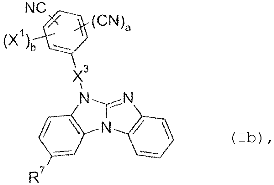 a vaut 0 ou 1 et b vaut 0 ou 1, la somme de a et b valant au moins 1 ;X1 est un groupe représenté par la formule suivante :

 X3 est une liaison simple etR7 est H ou un groupe représenté par la formule suivante :
 R70 et R71 sont chacun indépendamment de l'autre un groupe alkyle en C1-C18, un groupe aryle en C6-C18 ou un groupe aryle en C6-C18 qui est substitué par alkyle en C1-C18 etR72 est un groupe alkyle en C1-C18, un groupe aryle en C6-C18 ou un groupe aryle en C6-C18 qui est substitué par alkyle en C1-C18.
 - Dispositif électronique, comprenant un composé selon la revendication 1.
- Dispositif électronique selon la revendication 2, qui est un dispositif électroluminescent.
- Couche de transport de charges, couche de blocage de charges/excitons ou couche d'émission comprenant un composé selon la revendication 1.
- Couche d'émission selon la revendication 4, comprenant un composé selon la revendication 1 en tant que matériau hôte.
- Appareil choisi dans le groupe constitué par les écrans de visualisation fixes ; les écrans de visualisation mobiles ; les unités d'éclairage ; les claviers ; les vêtements ; les meubles ; le papier peint, comprenant le dispositif électronique organique selon la revendication 2 ou 3 ou la couche de transport de charges, la couche de blocage de charges/excitons ou la couche d'émission selon la revendication 4 ou 5.
- Utilisation des composés selon la revendication 1 dans des photorécepteurs électrophotographiques, des convertisseurs photoélectriques, des cellules solaires organiques, des éléments de commutation, des transistors à effet de champ émettant de la lumière organiques, des capteurs d'image, des lasers à colorant ou des dispositifs électroluminescents.
- Couche d'émission selon la revendication 4, comprenant au moins un composé de formule I en tant qu'émetteur de TADF ou en tant que matériau hôte à TADF en association avec au moins un émetteur fluorescent.
Priority Applications (3)
| Application Number | Priority Date | Filing Date | Title |
|---|---|---|---|
| EP15161950.9A EP3075737B1 (fr) | 2015-03-31 | 2015-03-31 | Benzimidazolo [1,2-a] benzimidazole portant des groupes heteroarylnitril aryl- ou pour diodes électroluminescentes organiques |
| PCT/IB2016/051831 WO2016157113A1 (fr) | 2015-03-31 | 2016-03-31 | Benzimidazolo[1,2-a]benzimidazole portant des groupes aryl- ou hétéroarylnitrile pour diodes électroluminescentes organiques |
| US15/563,072 US10689385B2 (en) | 2015-03-31 | 2016-03-31 | Benzimidazolo[1,2-A]benzimidazole carrying aryl- or arylnitril groups for organic light emitting diodes |
Applications Claiming Priority (1)
| Application Number | Priority Date | Filing Date | Title |
|---|---|---|---|
| EP15161950.9A EP3075737B1 (fr) | 2015-03-31 | 2015-03-31 | Benzimidazolo [1,2-a] benzimidazole portant des groupes heteroarylnitril aryl- ou pour diodes électroluminescentes organiques |
Publications (2)
| Publication Number | Publication Date |
|---|---|
| EP3075737A1 EP3075737A1 (fr) | 2016-10-05 |
| EP3075737B1 true EP3075737B1 (fr) | 2019-12-04 |
Family
ID=52811015
Family Applications (1)
| Application Number | Title | Priority Date | Filing Date |
|---|---|---|---|
| EP15161950.9A Active EP3075737B1 (fr) | 2015-03-31 | 2015-03-31 | Benzimidazolo [1,2-a] benzimidazole portant des groupes heteroarylnitril aryl- ou pour diodes électroluminescentes organiques |
Country Status (3)
| Country | Link |
|---|---|
| US (1) | US10689385B2 (fr) |
| EP (1) | EP3075737B1 (fr) |
| WO (1) | WO2016157113A1 (fr) |
Families Citing this family (12)
| Publication number | Priority date | Publication date | Assignee | Title |
|---|---|---|---|---|
| EP2872512B1 (fr) * | 2012-07-10 | 2017-05-10 | UDC Ireland Limited | Dérivés de benzimidazo[1,2-a]benzimidazole pour applications électroniques |
| EP3034507A1 (fr) * | 2014-12-15 | 2016-06-22 | Idemitsu Kosan Co., Ltd | Dibenzothiophènes et dibenzofurannes 1-functionalisés pour diodes électroluminescentes organiques (OLED) |
| US10608188B2 (en) | 2017-09-11 | 2020-03-31 | Universal Display Corporation | Organic electroluminescent materials and devices |
| KR102172580B1 (ko) * | 2018-02-13 | 2020-11-02 | 주식회사 엘지화학 | 헤테로고리 화합물 및 이를 포함하는 유기 발광 소자 |
| EP3587423A1 (fr) | 2018-06-27 | 2020-01-01 | Idemitsu Kosan Co., Ltd. | Composés organiques et dispositif électroluminescent organique les comprenant |
| EP3696167B1 (fr) | 2018-07-27 | 2024-11-20 | Idemitsu Kosan Co.,Ltd. | Composé, matériau pour élément électroluminescent organique, élément électroluminescent organique, et dispositif électronique |
| EP3651225A1 (fr) * | 2018-11-09 | 2020-05-13 | Idemitsu Kosan Co., Ltd. | Nouveaux composés organiques et dispositif électroluminescent organique les comprenant |
| US11706980B2 (en) | 2018-11-28 | 2023-07-18 | Universal Display Corporation | Host materials for electroluminescent devices |
| CN109651406B (zh) * | 2019-01-23 | 2021-01-08 | 苏州久显新材料有限公司 | 热激活延迟荧光化合物、发光材料及有机电致发光器件 |
| KR102721075B1 (ko) * | 2019-02-15 | 2024-10-24 | 삼성전자주식회사 | 축합환 화합물 및 이를 포함한 유기 발광 소자 |
| US11512093B2 (en) | 2019-03-04 | 2022-11-29 | Universal Display Corporation | Compound used for organic light emitting device (OLED), consumer product and formulation |
| KR102739951B1 (ko) | 2019-04-03 | 2024-12-06 | 삼성전자주식회사 | 축합환 화합물 및 이를 포함한 유기 발광 소자 |
Family Cites Families (159)
| Publication number | Priority date | Publication date | Assignee | Title |
|---|---|---|---|---|
| CN101312235B (zh) | 1999-05-13 | 2010-06-09 | 普林斯顿大学理事会 | 基于电致磷光的极高效有机发光器件 |
| JP3924648B2 (ja) | 1999-11-02 | 2007-06-06 | ソニー株式会社 | 有機電界発光素子 |
| JP4357781B2 (ja) | 1999-12-01 | 2009-11-04 | ザ、トラスティーズ オブ プリンストン ユニバーシティ | 有機led用燐光性ドーパントとしての式l2mxの錯体 |
| US6821645B2 (en) | 1999-12-27 | 2004-11-23 | Fuji Photo Film Co., Ltd. | Light-emitting material comprising orthometalated iridium complex, light-emitting device, high efficiency red light-emitting device, and novel iridium complex |
| US6565994B2 (en) | 2000-02-10 | 2003-05-20 | Fuji Photo Film Co., Ltd. | Light emitting device material comprising iridium complex and light emitting device using same material |
| US20020121638A1 (en) | 2000-06-30 | 2002-09-05 | Vladimir Grushin | Electroluminescent iridium compounds with fluorinated phenylpyridines, phenylpyrimidines, and phenylquinolines and devices made with such compounds |
| US7306856B2 (en) | 2000-07-17 | 2007-12-11 | Fujifilm Corporation | Light-emitting element and iridium complex |
| JP5241053B2 (ja) | 2000-08-11 | 2013-07-17 | ザ、トラスティーズ オブ プリンストン ユニバーシティ | 有機金属化合物及び放射移行有機電気燐光体 |
| JP4344494B2 (ja) | 2000-08-24 | 2009-10-14 | 富士フイルム株式会社 | 発光素子及び新規重合体子 |
| JP4067286B2 (ja) | 2000-09-21 | 2008-03-26 | 富士フイルム株式会社 | 発光素子及びイリジウム錯体 |
| JP4154138B2 (ja) | 2000-09-26 | 2008-09-24 | キヤノン株式会社 | 発光素子、表示装置及び金属配位化合物 |
| JP4154139B2 (ja) | 2000-09-26 | 2008-09-24 | キヤノン株式会社 | 発光素子 |
| JP4086499B2 (ja) | 2000-11-29 | 2008-05-14 | キヤノン株式会社 | 金属配位化合物、発光素子及び表示装置 |
| JP4154145B2 (ja) | 2000-12-01 | 2008-09-24 | キヤノン株式会社 | 金属配位化合物、発光素子及び表示装置 |
| DE10104426A1 (de) | 2001-02-01 | 2002-08-08 | Covion Organic Semiconductors | Verfahren zur Herstellung von hochreinen, tris-ortho-metallierten Organo-Iridium-Verbindungen |
| JP4307000B2 (ja) | 2001-03-08 | 2009-08-05 | キヤノン株式会社 | 金属配位化合物、電界発光素子及び表示装置 |
| US6687266B1 (en) | 2002-11-08 | 2004-02-03 | Universal Display Corporation | Organic light emitting materials and devices |
| DE10338550A1 (de) | 2003-08-19 | 2005-03-31 | Basf Ag | Übergangsmetallkomplexe mit Carbenliganden als Emitter für organische Licht-emittierende Dioden (OLEDs) |
| WO2005113704A2 (fr) | 2004-05-18 | 2005-12-01 | The University Of Southern California | Composes luminescents a ligands carbene |
| US20060008670A1 (en) | 2004-07-06 | 2006-01-12 | Chun Lin | Organic light emitting materials and devices |
| JP5009154B2 (ja) | 2004-07-07 | 2012-08-22 | ユニバーサル ディスプレイ コーポレイション | 安定で効率的なエレクトロルミネセンス材料 |
| DE102004057072A1 (de) | 2004-11-25 | 2006-06-01 | Basf Ag | Verwendung von Übergangsmetall-Carbenkomplexen in organischen Licht-emittierenden Dioden (OLEDs) |
| CA2589711A1 (fr) | 2004-12-23 | 2006-06-29 | Ciba Specialty Chemicals Holding Inc. | Complexes metalliques electroluminescents a ligands carbene nucleophiles |
| WO2006098460A1 (fr) | 2005-03-17 | 2006-09-21 | Semiconductor Energy Laboratory Co., Ltd. | Complexe organometallique, et element electroluminescent, dispositif electroluminescent et dispositif electronique utilisant le complexe organometallique |
| DE102005014284A1 (de) | 2005-03-24 | 2006-09-28 | Basf Ag | Verwendung von Verbindungen, welche aromatische oder heteroaromatische über Carbonyl-Gruppen enthaltende Gruppen verbundene Ringe enthalten, als Matrixmaterialien in organischen Leuchtdioden |
| WO2006114966A1 (fr) | 2005-04-18 | 2006-11-02 | Konica Minolta Holdings, Inc. | Dispositif électroluminescent organique, affichage et dispositif d'illumination |
| TWI418606B (zh) | 2005-04-25 | 2013-12-11 | Udc Ireland Ltd | 有機電致發光裝置 |
| US8586204B2 (en) | 2007-12-28 | 2013-11-19 | Universal Display Corporation | Phosphorescent emitters and host materials with improved stability |
| US9051344B2 (en) | 2005-05-06 | 2015-06-09 | Universal Display Corporation | Stability OLED materials and devices |
| WO2006128800A1 (fr) | 2005-05-30 | 2006-12-07 | Ciba Specialty Chemicals Holding Inc. | Dispositif electroluminescent |
| JP4887731B2 (ja) | 2005-10-26 | 2012-02-29 | コニカミノルタホールディングス株式会社 | 有機エレクトロルミネッセンス素子、表示装置及び照明装置 |
| EP1786050B1 (fr) | 2005-11-10 | 2010-06-23 | Novaled AG | Matériau semiconducteur organique dopé |
| US7935434B2 (en) | 2006-01-05 | 2011-05-03 | Konica Minolta Holdings, Inc. | Organic electroluminescent device, display, and illuminating device |
| KR102103062B1 (ko) | 2006-02-10 | 2020-04-22 | 유니버셜 디스플레이 코포레이션 | 시클로금속화 이미다조[1,2-f]페난트리딘 및 디이미다조[1,2-a:1',2'-c]퀴나졸린 리간드, 및 이의 등전자성 및 벤즈고리화된 유사체의 금속 착체 |
| WO2007108362A1 (fr) | 2006-03-17 | 2007-09-27 | Konica Minolta Holdings, Inc. | Dispositif électroluminescent organique, dispositif d'éclairage et d'affichage |
| EP1837927A1 (fr) | 2006-03-22 | 2007-09-26 | Novaled AG | Utilisation de radicaux hétérocycliques pour doper des semiconducteurs organiques |
| EP1837926B1 (fr) | 2006-03-21 | 2008-05-07 | Novaled AG | Radicaux ou diradicaux hétérocycliques, leur dimères, oligomères, polymères, composés spiro et polycycliques. Leur usage dans des semi-conducteurs organiques et dispositifs électroniques. |
| JP5683784B2 (ja) | 2006-03-23 | 2015-03-11 | コニカミノルタ株式会社 | 有機エレクトロルミネッセンス素子、表示装置及び照明装置 |
| US20070224446A1 (en) | 2006-03-24 | 2007-09-27 | Idemitsu Kosan Co., Ltd. | Material for organic electroluminescence device and organic electroluminescence device using the same |
| WO2007114244A1 (fr) | 2006-03-30 | 2007-10-11 | Konica Minolta Holdings, Inc. | Dispositif electroluminescent organique, dispositif d'eclairage et dispositif d'affichage |
| CN101460514A (zh) | 2006-04-04 | 2009-06-17 | 巴斯夫欧洲公司 | 含有一个非碳烯配体和一个或两个碳烯配体的过渡金属配合物及它们在oled中的用途 |
| ATE550342T1 (de) | 2006-04-05 | 2012-04-15 | Basf Se | Heteroleptische übergangsmetall-carben-komplexe und deren verwendung in organischen leuchtdioden (oleds) |
| JP5055818B2 (ja) | 2006-04-19 | 2012-10-24 | コニカミノルタホールディングス株式会社 | 有機エレクトロルミネッセンス素子材料、有機エレクトロルミネッセンス素子、表示装置及び照明装置 |
| EP2639231B1 (fr) | 2006-04-26 | 2019-02-06 | Idemitsu Kosan Co., Ltd. | Dérivé d'amine aromatique et élément électroluminescent organique l'utilisant |
| EP2034538B1 (fr) | 2006-06-02 | 2013-10-09 | Idemitsu Kosan Co., Ltd. | Matériau pour élément organique électroluminescent et élément organique électroluminescent utilisant le matériau |
| WO2008000727A1 (fr) | 2006-06-26 | 2008-01-03 | Basf Se | Utilisation dans des diodes électroluminescentes organiques de complexes carbène -métaux de transition qui ne contiennent pas de cyclométallation par l'intermédiaire de non carbènes |
| JP2008021687A (ja) | 2006-07-10 | 2008-01-31 | Mitsubishi Chemicals Corp | 有機電界発光素子用材料、有機電界発光素子用組成物及び有機電界発光素子 |
| WO2008022065A2 (fr) | 2006-08-11 | 2008-02-21 | Light Prescriptions Innovators, Llc | Amélioration de luminance de led et mélange de couleurs par combinaison de faisceau multiplexée de manière rotative |
| KR20090040895A (ko) | 2006-08-23 | 2009-04-27 | 이데미쓰 고산 가부시키가이샤 | 방향족 아민 유도체 및 이들을 이용한 유기 전기발광 소자 |
| JP2008066569A (ja) | 2006-09-08 | 2008-03-21 | Konica Minolta Holdings Inc | 有機エレクトロルミネッセンス素子、照明装置及び表示装置 |
| JP5444715B2 (ja) | 2006-09-08 | 2014-03-19 | コニカミノルタ株式会社 | 有機エレクトロルミネッセンス素子、照明装置及び表示装置 |
| WO2008029652A1 (fr) | 2006-09-08 | 2008-03-13 | Konica Minolta Holdings, Inc. | Dispositif électroluminescent organique, dispositif d'éclairage et écran d'affichage |
| JP5556014B2 (ja) | 2006-09-20 | 2014-07-23 | コニカミノルタ株式会社 | 有機エレクトロルミネッセンス素子 |
| JP5589251B2 (ja) | 2006-09-21 | 2014-09-17 | コニカミノルタ株式会社 | 有機エレクトロルミネッセンス素子材料 |
| KR101069302B1 (ko) | 2006-09-21 | 2011-10-05 | 바스프 에스이 | 수명이 연장된 oled 디스플레이 |
| JP5011908B2 (ja) | 2006-09-26 | 2012-08-29 | コニカミノルタホールディングス株式会社 | 有機エレクトロルミネッセンス素子、表示装置および照明装置 |
| JP5063992B2 (ja) | 2006-11-20 | 2012-10-31 | ケミプロ化成株式会社 | 新規なジ(ピリジルフェニル)誘導体、それよりなる電子輸送材料およびそれを含む有機エレクトロルミネッセンス素子 |
| JP5493357B2 (ja) | 2006-12-13 | 2014-05-14 | コニカミノルタ株式会社 | 有機エレクトロルミネッセンス素子、表示装置及び照明装置 |
| WO2008090912A1 (fr) | 2007-01-23 | 2008-07-31 | Konica Minolta Holdings, Inc. | Procédé de fabrication de dispositif électroluminescent organique, dispositif électroluminescent organique fabriqué par le procédé, dispositif d'affichage et dispositif illuminateur |
| JP2008207520A (ja) | 2007-02-28 | 2008-09-11 | Konica Minolta Holdings Inc | 有機薄膜、有機薄膜の製造方法、電子デバイス、有機エレクトロルミネッセンス素子、表示装置及び照明装置 |
| DE102007012794B3 (de) | 2007-03-16 | 2008-06-19 | Novaled Ag | Pyrido[3,2-h]chinazoline und/oder deren 5,6-Dihydroderivate, deren Herstellungsverfahren und diese enthaltendes dotiertes organisches Halbleitermaterial |
| EP3076451B1 (fr) | 2007-04-30 | 2019-03-06 | Novaled GmbH | Connexions de matiere d'oxydes de carbone, de matiere de pseudo oxyde de carbone et radiales tout comme leur utilisation |
| JP5564942B2 (ja) | 2007-05-16 | 2014-08-06 | コニカミノルタ株式会社 | 有機エレクトロルミネッセンス素子、表示装置及び照明装置 |
| WO2008146838A1 (fr) | 2007-05-30 | 2008-12-04 | Konica Minolta Holdings, Inc. | Dispositif électroluminescent organique, dispositif d'affichage et dispositif d'éclairage |
| WO2008156879A1 (fr) | 2007-06-20 | 2008-12-24 | Universal Display Corporation | Matériaux à base d'imidazophénantridine phosphorescente bleue |
| WO2008156105A1 (fr) | 2007-06-21 | 2008-12-24 | Konica Minolta Holdings, Inc. | Matériau d'élément électroluminescent organique, élément électroluminescent organique, dispositif d'affichage et dispositif d'éclairage |
| JP5804703B2 (ja) | 2007-07-05 | 2015-11-04 | ビーエーエスエフ ソシエタス・ヨーロピアBasf Se | ジシリルカルバゾール、ジシリルジベンゾフラン、ジシリルジベンゾチオフェン、ジシリルジベンゾホスホール、ジシリルジベンゾチオフェンs−オキシドおよびジシリルジベンゾチオフェンs,s−ジオキシドから選択される少なくとも1つのジシリル化合物を含む有機発光ダイオード |
| KR101577465B1 (ko) | 2007-07-05 | 2015-12-14 | 바스프 에스이 | 카르벤 전이 금속 착체 이미터, 및 디실릴카르바졸, 디실릴디벤조푸란, 디실릴디벤조티오펜, 디실릴디벤조포스폴, 디실릴디벤조티오펜 s-옥사이드 및 디실릴디벤조티오펜 s,s-디옥사이드로부터 선택된 1종 이상의 화합물을 포함하는 유기 발광 다이오드 |
| WO2009008099A1 (fr) | 2007-07-10 | 2009-01-15 | Idemitsu Kosan Co., Ltd. | Matériau pour élément à électroluminescence organique, et élément à électroluminescence organique préparé à l'aide du matériau |
| JP5194596B2 (ja) | 2007-07-11 | 2013-05-08 | コニカミノルタホールディングス株式会社 | 有機エレクトロルミネッセンス素子、表示装置及び照明装置 |
| JP2009040728A (ja) | 2007-08-09 | 2009-02-26 | Canon Inc | 有機金属錯体及びこれを用いた有機発光素子 |
| JP5186843B2 (ja) | 2007-08-30 | 2013-04-24 | コニカミノルタホールディングス株式会社 | 有機エレクトロルミネッセンス素子、照明装置及び表示装置 |
| JP5624270B2 (ja) | 2007-09-18 | 2014-11-12 | ユー・ディー・シー アイルランド リミテッド | 有機電界発光素子 |
| EP2203461B1 (fr) | 2007-10-17 | 2011-08-10 | Basf Se | Complexes de métaux de transition avec des ligands carbène pontés, et leur utilisation dans des diodes électroluminescentes organiques (oled) |
| US8258297B2 (en) | 2007-10-17 | 2012-09-04 | Basf Se | Transition metal complexes with bridged carbene ligands and use thereof in OLEDs |
| JP2009114370A (ja) | 2007-11-08 | 2009-05-28 | Konica Minolta Holdings Inc | 有機エレクトロルミネッセンス素子材料、有機エレクトロルミネッセンス素子及び表示装置、照明装置 |
| WO2009060780A1 (fr) | 2007-11-08 | 2009-05-14 | Konica Minolta Holdings, Inc. | Elément électroluminescent organique, dispositif d'affichage, et système d'éclairage |
| JP2009114369A (ja) | 2007-11-08 | 2009-05-28 | Konica Minolta Holdings Inc | 有機エレクトロルミネッセンス材料、有機エレクトロルミネッセンス素子、表示装置及び照明装置 |
| WO2009060779A1 (fr) | 2007-11-08 | 2009-05-14 | Konica Minolta Holdings, Inc. | Matériau de dispositif électroluminescent organique, dispositif électroluminescent organique, dispositif d'affichage et dispositif d'éclairage |
| JP5458890B2 (ja) | 2007-11-08 | 2014-04-02 | コニカミノルタ株式会社 | 有機エレクトロルミネッセンス素子、表示装置及び照明装置 |
| WO2009060757A1 (fr) | 2007-11-08 | 2009-05-14 | Konica Minolta Holdings, Inc. | Dispositif électroluminescent organique, dispositif d'affichage et dispositif d'éclairage |
| WO2009063757A1 (fr) | 2007-11-14 | 2009-05-22 | Konica Minolta Holdings, Inc. | Matériau de dispositif électroluminescent organique, dispositif électroluminescent organique, procédé de fabrication d'un dispositif électroluminescent organique, dispositif d'affichage et dispositif d'éclairage |
| JP2009135183A (ja) | 2007-11-29 | 2009-06-18 | Konica Minolta Holdings Inc | 有機エレクトロルミネッセンス素子、表示装置及び照明装置 |
| WO2009073245A1 (fr) | 2007-12-06 | 2009-06-11 | Universal Display Corporation | Complexes organométalliques électroluminescents |
| US20090153034A1 (en) | 2007-12-13 | 2009-06-18 | Universal Display Corporation | Carbazole-containing materials in phosphorescent light emittinig diodes |
| WO2009084413A1 (fr) | 2007-12-28 | 2009-07-09 | Konica Minolta Holdings, Inc. | Dispositif électroluminescent organique et procédé de fabrication de dispositif électroluminescent organique |
| US8221905B2 (en) | 2007-12-28 | 2012-07-17 | Universal Display Corporation | Carbazole-containing materials in phosphorescent light emitting diodes |
| JP5549053B2 (ja) | 2008-01-18 | 2014-07-16 | コニカミノルタ株式会社 | 有機エレクトロルミネッセンス素子用材料、有機エレクトロルミネッセンス素子、有機エレクトロルミネッセンス素子の製造方法、表示装置及び照明装置 |
| JP2009182298A (ja) | 2008-02-01 | 2009-08-13 | Konica Minolta Holdings Inc | 有機エレクトロルミネッセンス素子、照明装置及び表示装置 |
| JP5381719B2 (ja) | 2008-02-20 | 2014-01-08 | コニカミノルタ株式会社 | 白色発光有機エレクトロルミネッセンス素子 |
| JP2009267255A (ja) | 2008-04-28 | 2009-11-12 | Idemitsu Kosan Co Ltd | 有機エレクトロルミネッセンス素子用材料及びそれを用いた有機エレクトロルミネッセンス素子 |
| US8057712B2 (en) | 2008-04-29 | 2011-11-15 | Novaled Ag | Radialene compounds and their use |
| EP2460866B1 (fr) | 2008-05-13 | 2019-12-11 | Konica Minolta Holdings, Inc. | Élément électroluminescent organique, dispositif d'affichage et dispositif d'éclairage |
| EP2860171B1 (fr) | 2008-06-30 | 2017-02-01 | Universal Display Corporation | Matériaux de transport de trous contenant un triphénylène |
| CN102131891B (zh) | 2008-06-30 | 2014-01-29 | 通用显示公司 | 具有含硫基团的空穴传输材料 |
| WO2010001830A1 (fr) | 2008-07-01 | 2010-01-07 | コニカミノルタホールディングス株式会社 | Elément électroluminescent organique émettant de la lumière blanche, dispositif d’éclairage et écran |
| WO2010004877A1 (fr) | 2008-07-10 | 2010-01-14 | コニカミノルタホールディングス株式会社 | Élément électroluminescent organique, dispositif d'affichage et dispositif d'éclairage |
| JP2010021336A (ja) | 2008-07-10 | 2010-01-28 | Konica Minolta Holdings Inc | 有機エレクトロルミネッセンス素子、照明装置及び表示装置 |
| JP5338184B2 (ja) | 2008-08-06 | 2013-11-13 | コニカミノルタ株式会社 | 有機エレクトロルミネッセンス素子、表示装置、照明装置 |
| TW201012909A (en) | 2008-08-28 | 2010-04-01 | Asahi Glass Co Ltd | Abrasive composition and method for manufacturing semiconductor integrated circuit device |
| WO2010027583A1 (fr) | 2008-09-03 | 2010-03-11 | Universal Display Corporation | Matières phosphorescentes |
| EP2340579B1 (fr) | 2008-10-07 | 2018-09-12 | Osram Oled Gmbh | Siloles substitués par des systèmes cycliques condensés et leur utilisation en électronique organique |
| JPWO2010044342A1 (ja) | 2008-10-15 | 2012-03-15 | コニカミノルタホールディングス株式会社 | 有機エレクトロルミネッセンス素子、有機エレクトロルミネッセンス素子の製造方法、白色有機エレクトロルミネッセンス素子、表示装置及び照明装置 |
| EP2180029B1 (fr) | 2008-10-23 | 2011-07-27 | Novaled AG | Composés de Radialène et leur utilisation |
| JP5493333B2 (ja) | 2008-11-05 | 2014-05-14 | コニカミノルタ株式会社 | 有機エレクトロルミネッセンス素子、白色有機エレクトロルミネッセンス素子、表示装置及び照明装置 |
| KR101919207B1 (ko) | 2008-11-11 | 2018-11-15 | 유니버셜 디스플레이 코포레이션 | 인광성 에미터 |
| JP5707665B2 (ja) | 2008-12-03 | 2015-04-30 | コニカミノルタ株式会社 | 有機エレクトロルミネッセンス素子、該素子を備えた照明装置及び表示装置 |
| WO2010067746A1 (fr) | 2008-12-08 | 2010-06-17 | コニカミノルタホールディングス株式会社 | Élément électroluminescent organique, dispositif d’affichage et dispositif d’éclairage |
| US8815415B2 (en) | 2008-12-12 | 2014-08-26 | Universal Display Corporation | Blue emitter with high efficiency based on imidazo[1,2-f] phenanthridine iridium complexes |
| US9458182B2 (en) | 2009-01-07 | 2016-10-04 | Basf Se | Silyl- and heteroatom-substituted compounds selected from carbazoles, dibenzofurans, dibenzothiophenes and dibenzophospholes, and use thereof in organic electronics |
| JP5810529B2 (ja) | 2009-01-09 | 2015-11-11 | コニカミノルタ株式会社 | 有機エレクトロルミネッセンス素子、表示装置及び照明装置 |
| JP5472121B2 (ja) | 2009-01-28 | 2014-04-16 | コニカミノルタ株式会社 | 有機エレクトロルミネッセンス素子、表示装置および照明装置、ならびに有機エレクトロルミネッセンス素子の製造方法 |
| DE102009007038A1 (de) | 2009-02-02 | 2010-08-05 | Merck Patent Gmbh | Metallkomplexe |
| WO2010090077A1 (fr) | 2009-02-06 | 2010-08-12 | コニカミノルタホールディングス株式会社 | Élément électroluminescent organique, et dispositif d'éclairage et dispositif d'affichage comprenant chacun l'élément |
| JP5765223B2 (ja) | 2009-02-18 | 2015-08-19 | コニカミノルタ株式会社 | 有機エレクトロルミネッセンス素子の製造方法、並びに有機エレクトロルミネッセンス素子を備えた照明装置及び表示装置 |
| EP2401254B1 (fr) | 2009-02-26 | 2013-06-19 | Novaled AG | Composés quinoniques convenant comme impureté de dopage en électronique organique |
| US8709615B2 (en) | 2011-07-28 | 2014-04-29 | Universal Display Corporation | Heteroleptic iridium complexes as dopants |
| TWI751419B (zh) | 2009-04-06 | 2022-01-01 | 美商環球展覽公司 | 包含新穎配位體結構之金屬錯合物 |
| EP2246862A1 (fr) | 2009-04-27 | 2010-11-03 | Novaled AG | Dispositif électronique organique comportant un matériau semi-conducteur organique |
| TWI687408B (zh) | 2009-04-28 | 2020-03-11 | 美商環球展覽公司 | 具有甲基-d3取代之銥錯合物 |
| US8603642B2 (en) | 2009-05-13 | 2013-12-10 | Global Oled Technology Llc | Internal connector for organic electronic devices |
| EP2493906B1 (fr) | 2009-10-28 | 2015-10-21 | Basf Se | Composees coordinatives heteroleptiques du type carben et leur usage dans electronique organique |
| EP2513125B1 (fr) | 2009-12-14 | 2014-10-29 | Basf Se | Complexes des metaux avec un ligand carbene diazabenzimidazole et leur usage en dispositifs d'éclairage à diodes électroluminescentes organiques |
| US8288187B2 (en) | 2010-01-20 | 2012-10-16 | Universal Display Corporation | Electroluminescent devices for lighting applications |
| US9156870B2 (en) | 2010-02-25 | 2015-10-13 | Universal Display Corporation | Phosphorescent emitters |
| TWI415846B (zh) | 2010-03-01 | 2013-11-21 | Semiconductor Energy Lab | 雜環化合物、發光元件、發光裝置、電子裝置、及照明裝置 |
| US9175211B2 (en) | 2010-03-03 | 2015-11-03 | Universal Display Corporation | Phosphorescent materials |
| US8334545B2 (en) | 2010-03-24 | 2012-12-18 | Universal Display Corporation | OLED display architecture |
| US8227801B2 (en) | 2010-04-26 | 2012-07-24 | Universal Display Corporation | Bicarbzole containing compounds for OLEDs |
| WO2011157779A1 (fr) | 2010-06-18 | 2011-12-22 | Basf Se | Dispositifs électroniques organiques comprenant une couche d'un composé de pyridine et un métal alcalino-terreux de 8—hydroxyquinolinolato ou un complexe alcalino-terreux |
| JP5990515B2 (ja) | 2010-06-18 | 2016-09-14 | ビーエーエスエフ ソシエタス・ヨーロピアBasf Se | ジベンゾフラン化合物と8−ヒドロキシキノリノラトアルカリ土類金属錯体または8−ヒドロキシキノリノラトアルカリ金属錯体との層を含む、有機電子デバイス |
| DE102010024542A1 (de) | 2010-06-22 | 2011-12-22 | Merck Patent Gmbh | Materialien für elektronische Vorrichtungen |
| RU2452872C2 (ru) | 2010-07-15 | 2012-06-10 | Андрей Леонидович Кузнецов | Пьезоэлектрический насос |
| JP5741581B2 (ja) | 2010-07-29 | 2015-07-01 | コニカミノルタ株式会社 | 透明導電膜、および有機エレクトロルミネッセンス素子 |
| ES2386564B1 (es) | 2010-08-06 | 2013-04-26 | Telefónica, S.A. | Método para gestionar información de presencia. |
| US8932734B2 (en) | 2010-10-08 | 2015-01-13 | Universal Display Corporation | Organic electroluminescent materials and devices |
| KR102071726B1 (ko) | 2010-10-22 | 2020-01-30 | 가부시키가이샤 한도오따이 에네루기 켄큐쇼 | 유기금속 착체, 발광 소자, 발광 장치, 전자 장치 및 조명 장치 |
| JP5900351B2 (ja) | 2011-02-02 | 2016-04-06 | コニカミノルタ株式会社 | 有機エレクトロルミネッセンス素子の製造方法 |
| US9368735B2 (en) | 2011-02-15 | 2016-06-14 | Konica Minolta, Inc. | Organic electroluminescence element and illumination device |
| WO2012115034A1 (fr) | 2011-02-22 | 2012-08-30 | コニカミノルタホールディングス株式会社 | Élément électroluminescent organique, dispositif d'éclairage et dispositif d'affichage |
| US8883322B2 (en) | 2011-03-08 | 2014-11-11 | Universal Display Corporation | Pyridyl carbene phosphorescent emitters |
| KR101951852B1 (ko) | 2011-03-25 | 2019-02-26 | 유디씨 아일랜드 리미티드 | 전자장치 응용을 위한 4h-이미다조[1,2-a]이미다졸 |
| WO2012147397A1 (fr) | 2011-04-26 | 2012-11-01 | コニカミノルタホールディングス株式会社 | Élément électroluminescent organique et appareil d'éclairage |
| US9212197B2 (en) | 2011-05-19 | 2015-12-15 | Universal Display Corporation | Phosphorescent heteroleptic phenylbenzimidazole dopants |
| US8748012B2 (en) | 2011-05-25 | 2014-06-10 | Universal Display Corporation | Host materials for OLED |
| US10079349B2 (en) | 2011-05-27 | 2018-09-18 | Universal Display Corporation | Organic electroluminescent materials and devices |
| KR20120135363A (ko) | 2011-06-01 | 2012-12-13 | 엘지디스플레이 주식회사 | 청색 인광 화합물 및 이를 이용한 유기전계 발광소자 |
| WO2012170571A1 (fr) | 2011-06-08 | 2012-12-13 | Universal Display Corporation | Complexes hétéroleptiques de carbènes d'iridium et dispositif électroluminescent utilisant ceux-ci |
| EP2721043B1 (fr) | 2011-06-14 | 2018-08-29 | UDC Ireland Limited | Complexes métalliques des ligand carbène azanbenzimidazole et l'utilisation de ceux-ci dans des diodes électroluminescentes organiques |
| US8409729B2 (en) | 2011-07-28 | 2013-04-02 | Universal Display Corporation | Host materials for phosphorescent OLEDs |
| WO2013022419A1 (fr) | 2011-08-05 | 2013-02-14 | Universal Display Corporation | Dispositifs électroluminescents organiques phosphorescents, combinés avec un matériau de transport de trous ayant une stabilité de fonctionnement élevée |
| KR102021099B1 (ko) | 2011-11-10 | 2019-09-16 | 유디씨 아일랜드 리미티드 | 전자장치 응용을 위한 4h-이미다조[1,2-a]이미다졸 |
| CN103959503B (zh) * | 2011-12-05 | 2016-08-24 | 出光兴产株式会社 | 有机电致发光元件用材料以及有机电致发光元件 |
| JP2014135466A (ja) | 2012-04-09 | 2014-07-24 | Kyushu Univ | 有機発光素子ならびにそれに用いる発光材料および化合物 |
| WO2013154084A1 (fr) | 2012-04-10 | 2013-10-17 | 株式会社Ihi | Compresseur |
| EP2872512B1 (fr) | 2012-07-10 | 2017-05-10 | UDC Ireland Limited | Dérivés de benzimidazo[1,2-a]benzimidazole pour applications électroniques |
| KR102127406B1 (ko) | 2012-09-20 | 2020-06-29 | 유디씨 아일랜드 리미티드 | 전자 응용을 위한 아자디벤조푸란 |
| EP3034506A1 (fr) | 2014-12-15 | 2016-06-22 | Idemitsu Kosan Co., Ltd | Dérivés de carbazole 4-fonctionnalisés pour applications électroniques |
| EP3034507A1 (fr) | 2014-12-15 | 2016-06-22 | Idemitsu Kosan Co., Ltd | Dibenzothiophènes et dibenzofurannes 1-functionalisés pour diodes électroluminescentes organiques (OLED) |
-
2015
- 2015-03-31 EP EP15161950.9A patent/EP3075737B1/fr active Active
-
2016
- 2016-03-31 WO PCT/IB2016/051831 patent/WO2016157113A1/fr not_active Ceased
- 2016-03-31 US US15/563,072 patent/US10689385B2/en active Active
Non-Patent Citations (1)
| Title |
|---|
| None * |
Also Published As
| Publication number | Publication date |
|---|---|
| EP3075737A1 (fr) | 2016-10-05 |
| US20180086763A1 (en) | 2018-03-29 |
| US10689385B2 (en) | 2020-06-23 |
| WO2016157113A1 (fr) | 2016-10-06 |
Similar Documents
| Publication | Publication Date | Title |
|---|---|---|
| US11744152B2 (en) | Benzimidazo[1,2-a]benzimidazole derivatives for electronic applications | |
| EP3075737B1 (fr) | Benzimidazolo [1,2-a] benzimidazole portant des groupes heteroarylnitril aryl- ou pour diodes électroluminescentes organiques | |
| EP3119770B1 (fr) | Dibenzofuranes et dibenzothiophènes | |
| EP2776443B1 (fr) | 4h-imidazo[1,2-a]imidazoles pour applications électroniques | |
| EP3072943B1 (fr) | Benzonitriles de dibenzofurane/carbazole-substitué | |
| EP3174885B1 (fr) | Benzimidazolo[1,2-a]benzimidazoles 2,9-fonctionnalisés en tant qu'hôtes pour des diodes électroluminescentes organiques | |
| EP3034507A1 (fr) | Dibenzothiophènes et dibenzofurannes 1-functionalisés pour diodes électroluminescentes organiques (OLED) | |
| US11174258B2 (en) | Benzimidazolo[1,2-a]benzimidazole derivatives for organic light emitting diodes | |
| EP3356368B1 (fr) | Groupes benzimidazolo [1,2-a] benzimidazoles portant des benzimidazolo [1,2-a] benzimidazolyles, groupes carbazolyles, groupes benzofuranes ou benzothiophènes pour diodes électroluminescentes organiques | |
| US20180277768A1 (en) | Benzimidazolo[1,2-a]benzimidazole carrying benzimidazolo[1,2-a]benzimidazolyl groups, carbazolyl groups, dibenzofurane groups or benzothiophene groups for organic light emitting diodes | |
| EP3356369B1 (fr) | Benzimidazol[1,2-a]benzimidazole à groupes triazine pour diodes électroluminescentes organiques | |
| EP3070144B1 (fr) | Composés cycliques à sept chaînons | |
| EP3034506A1 (fr) | Dérivés de carbazole 4-fonctionnalisés pour applications électroniques | |
| US10968229B2 (en) | Seven-membered ring compounds | |
| EP3061759B1 (fr) | Dibenzofuranes à substituant nitrile | |
| WO2016079667A1 (fr) | Dérivés d'indole pour des applications électroniques | |
| WO2016067261A1 (fr) | 5-((benz)imidazol-2-yl) benzimidazo[1,2-a]benzimidazoles utilisés pour des applications électroniques |
Legal Events
| Date | Code | Title | Description |
|---|---|---|---|
| PUAI | Public reference made under article 153(3) epc to a published international application that has entered the european phase |
Free format text: ORIGINAL CODE: 0009012 |
|
| AK | Designated contracting states |
Kind code of ref document: A1 Designated state(s): AL AT BE BG CH CY CZ DE DK EE ES FI FR GB GR HR HU IE IS IT LI LT LU LV MC MK MT NL NO PL PT RO RS SE SI SK SM TR |
|
| AX | Request for extension of the european patent |
Extension state: BA ME |
|
| STAA | Information on the status of an ep patent application or granted ep patent |
Free format text: STATUS: REQUEST FOR EXAMINATION WAS MADE |
|
| 17P | Request for examination filed |
Effective date: 20170404 |
|
| RBV | Designated contracting states (corrected) |
Designated state(s): AL AT BE BG CH CY CZ DE DK EE ES FI FR GB GR HR HU IE IS IT LI LT LU LV MC MK MT NL NO PL PT RO RS SE SI SK SM TR |
|
| STAA | Information on the status of an ep patent application or granted ep patent |
Free format text: STATUS: EXAMINATION IS IN PROGRESS |
|
| 17Q | First examination report despatched |
Effective date: 20170725 |
|
| GRAP | Despatch of communication of intention to grant a patent |
Free format text: ORIGINAL CODE: EPIDOSNIGR1 |
|
| STAA | Information on the status of an ep patent application or granted ep patent |
Free format text: STATUS: GRANT OF PATENT IS INTENDED |
|
| INTG | Intention to grant announced |
Effective date: 20190116 |
|
| GRAS | Grant fee paid |
Free format text: ORIGINAL CODE: EPIDOSNIGR3 |
|
| GRAJ | Information related to disapproval of communication of intention to grant by the applicant or resumption of examination proceedings by the epo deleted |
Free format text: ORIGINAL CODE: EPIDOSDIGR1 |
|
| GRAL | Information related to payment of fee for publishing/printing deleted |
Free format text: ORIGINAL CODE: EPIDOSDIGR3 |
|
| STAA | Information on the status of an ep patent application or granted ep patent |
Free format text: STATUS: EXAMINATION IS IN PROGRESS |
|
| GRAP | Despatch of communication of intention to grant a patent |
Free format text: ORIGINAL CODE: EPIDOSNIGR1 |
|
| STAA | Information on the status of an ep patent application or granted ep patent |
Free format text: STATUS: GRANT OF PATENT IS INTENDED |
|
| INTC | Intention to grant announced (deleted) | ||
| INTG | Intention to grant announced |
Effective date: 20190903 |
|
| GRAA | (expected) grant |
Free format text: ORIGINAL CODE: 0009210 |
|
| STAA | Information on the status of an ep patent application or granted ep patent |
Free format text: STATUS: THE PATENT HAS BEEN GRANTED |
|
| AK | Designated contracting states |
Kind code of ref document: B1 Designated state(s): AL AT BE BG CH CY CZ DE DK EE ES FI FR GB GR HR HU IE IS IT LI LT LU LV MC MK MT NL NO PL PT RO RS SE SI SK SM TR |
|
| REG | Reference to a national code |
Ref country code: GB Ref legal event code: FG4D |
|
| REG | Reference to a national code |
Ref country code: CH Ref legal event code: EP |
|
| REG | Reference to a national code |
Ref country code: AT Ref legal event code: REF Ref document number: 1209265 Country of ref document: AT Kind code of ref document: T Effective date: 20191215 |
|
| REG | Reference to a national code |
Ref country code: DE Ref legal event code: R096 Ref document number: 602015042808 Country of ref document: DE |
|
| REG | Reference to a national code |
Ref country code: IE Ref legal event code: FG4D |
|
| REG | Reference to a national code |
Ref country code: NL Ref legal event code: MP Effective date: 20191204 |
|
| REG | Reference to a national code |
Ref country code: LT Ref legal event code: MG4D |
|
| PG25 | Lapsed in a contracting state [announced via postgrant information from national office to epo] |
Ref country code: SE Free format text: LAPSE BECAUSE OF FAILURE TO SUBMIT A TRANSLATION OF THE DESCRIPTION OR TO PAY THE FEE WITHIN THE PRESCRIBED TIME-LIMIT Effective date: 20191204 Ref country code: LV Free format text: LAPSE BECAUSE OF FAILURE TO SUBMIT A TRANSLATION OF THE DESCRIPTION OR TO PAY THE FEE WITHIN THE PRESCRIBED TIME-LIMIT Effective date: 20191204 Ref country code: NO Free format text: LAPSE BECAUSE OF FAILURE TO SUBMIT A TRANSLATION OF THE DESCRIPTION OR TO PAY THE FEE WITHIN THE PRESCRIBED TIME-LIMIT Effective date: 20200304 Ref country code: GR Free format text: LAPSE BECAUSE OF FAILURE TO SUBMIT A TRANSLATION OF THE DESCRIPTION OR TO PAY THE FEE WITHIN THE PRESCRIBED TIME-LIMIT Effective date: 20200305 Ref country code: LT Free format text: LAPSE BECAUSE OF FAILURE TO SUBMIT A TRANSLATION OF THE DESCRIPTION OR TO PAY THE FEE WITHIN THE PRESCRIBED TIME-LIMIT Effective date: 20191204 Ref country code: FI Free format text: LAPSE BECAUSE OF FAILURE TO SUBMIT A TRANSLATION OF THE DESCRIPTION OR TO PAY THE FEE WITHIN THE PRESCRIBED TIME-LIMIT Effective date: 20191204 Ref country code: BG Free format text: LAPSE BECAUSE OF FAILURE TO SUBMIT A TRANSLATION OF THE DESCRIPTION OR TO PAY THE FEE WITHIN THE PRESCRIBED TIME-LIMIT Effective date: 20200304 |
|
| PG25 | Lapsed in a contracting state [announced via postgrant information from national office to epo] |
Ref country code: RS Free format text: LAPSE BECAUSE OF FAILURE TO SUBMIT A TRANSLATION OF THE DESCRIPTION OR TO PAY THE FEE WITHIN THE PRESCRIBED TIME-LIMIT Effective date: 20191204 Ref country code: HR Free format text: LAPSE BECAUSE OF FAILURE TO SUBMIT A TRANSLATION OF THE DESCRIPTION OR TO PAY THE FEE WITHIN THE PRESCRIBED TIME-LIMIT Effective date: 20191204 |
|
| PG25 | Lapsed in a contracting state [announced via postgrant information from national office to epo] |
Ref country code: AL Free format text: LAPSE BECAUSE OF FAILURE TO SUBMIT A TRANSLATION OF THE DESCRIPTION OR TO PAY THE FEE WITHIN THE PRESCRIBED TIME-LIMIT Effective date: 20191204 |
|
| PG25 | Lapsed in a contracting state [announced via postgrant information from national office to epo] |
Ref country code: PT Free format text: LAPSE BECAUSE OF FAILURE TO SUBMIT A TRANSLATION OF THE DESCRIPTION OR TO PAY THE FEE WITHIN THE PRESCRIBED TIME-LIMIT Effective date: 20200429 Ref country code: EE Free format text: LAPSE BECAUSE OF FAILURE TO SUBMIT A TRANSLATION OF THE DESCRIPTION OR TO PAY THE FEE WITHIN THE PRESCRIBED TIME-LIMIT Effective date: 20191204 Ref country code: ES Free format text: LAPSE BECAUSE OF FAILURE TO SUBMIT A TRANSLATION OF THE DESCRIPTION OR TO PAY THE FEE WITHIN THE PRESCRIBED TIME-LIMIT Effective date: 20191204 Ref country code: CZ Free format text: LAPSE BECAUSE OF FAILURE TO SUBMIT A TRANSLATION OF THE DESCRIPTION OR TO PAY THE FEE WITHIN THE PRESCRIBED TIME-LIMIT Effective date: 20191204 Ref country code: RO Free format text: LAPSE BECAUSE OF FAILURE TO SUBMIT A TRANSLATION OF THE DESCRIPTION OR TO PAY THE FEE WITHIN THE PRESCRIBED TIME-LIMIT Effective date: 20191204 Ref country code: NL Free format text: LAPSE BECAUSE OF FAILURE TO SUBMIT A TRANSLATION OF THE DESCRIPTION OR TO PAY THE FEE WITHIN THE PRESCRIBED TIME-LIMIT Effective date: 20191204 |
|
| PG25 | Lapsed in a contracting state [announced via postgrant information from national office to epo] |
Ref country code: IS Free format text: LAPSE BECAUSE OF FAILURE TO SUBMIT A TRANSLATION OF THE DESCRIPTION OR TO PAY THE FEE WITHIN THE PRESCRIBED TIME-LIMIT Effective date: 20200404 Ref country code: SK Free format text: LAPSE BECAUSE OF FAILURE TO SUBMIT A TRANSLATION OF THE DESCRIPTION OR TO PAY THE FEE WITHIN THE PRESCRIBED TIME-LIMIT Effective date: 20191204 Ref country code: SM Free format text: LAPSE BECAUSE OF FAILURE TO SUBMIT A TRANSLATION OF THE DESCRIPTION OR TO PAY THE FEE WITHIN THE PRESCRIBED TIME-LIMIT Effective date: 20191204 |
|
| REG | Reference to a national code |
Ref country code: DE Ref legal event code: R097 Ref document number: 602015042808 Country of ref document: DE |
|
| REG | Reference to a national code |
Ref country code: AT Ref legal event code: MK05 Ref document number: 1209265 Country of ref document: AT Kind code of ref document: T Effective date: 20191204 |
|
| PLBE | No opposition filed within time limit |
Free format text: ORIGINAL CODE: 0009261 |
|
| STAA | Information on the status of an ep patent application or granted ep patent |
Free format text: STATUS: NO OPPOSITION FILED WITHIN TIME LIMIT |
|
| PG25 | Lapsed in a contracting state [announced via postgrant information from national office to epo] |
Ref country code: DK Free format text: LAPSE BECAUSE OF FAILURE TO SUBMIT A TRANSLATION OF THE DESCRIPTION OR TO PAY THE FEE WITHIN THE PRESCRIBED TIME-LIMIT Effective date: 20191204 Ref country code: MC Free format text: LAPSE BECAUSE OF FAILURE TO SUBMIT A TRANSLATION OF THE DESCRIPTION OR TO PAY THE FEE WITHIN THE PRESCRIBED TIME-LIMIT Effective date: 20191204 |
|
| REG | Reference to a national code |
Ref country code: CH Ref legal event code: PL |
|
| 26N | No opposition filed |
Effective date: 20200907 |
|
| PG25 | Lapsed in a contracting state [announced via postgrant information from national office to epo] |
Ref country code: PL Free format text: LAPSE BECAUSE OF FAILURE TO SUBMIT A TRANSLATION OF THE DESCRIPTION OR TO PAY THE FEE WITHIN THE PRESCRIBED TIME-LIMIT Effective date: 20191204 Ref country code: SI Free format text: LAPSE BECAUSE OF FAILURE TO SUBMIT A TRANSLATION OF THE DESCRIPTION OR TO PAY THE FEE WITHIN THE PRESCRIBED TIME-LIMIT Effective date: 20191204 Ref country code: AT Free format text: LAPSE BECAUSE OF FAILURE TO SUBMIT A TRANSLATION OF THE DESCRIPTION OR TO PAY THE FEE WITHIN THE PRESCRIBED TIME-LIMIT Effective date: 20191204 |
|
| REG | Reference to a national code |
Ref country code: BE Ref legal event code: MM Effective date: 20200331 |
|
| PG25 | Lapsed in a contracting state [announced via postgrant information from national office to epo] |
Ref country code: LU Free format text: LAPSE BECAUSE OF NON-PAYMENT OF DUE FEES Effective date: 20200331 |
|
| PG25 | Lapsed in a contracting state [announced via postgrant information from national office to epo] |
Ref country code: LI Free format text: LAPSE BECAUSE OF NON-PAYMENT OF DUE FEES Effective date: 20200331 Ref country code: IT Free format text: LAPSE BECAUSE OF FAILURE TO SUBMIT A TRANSLATION OF THE DESCRIPTION OR TO PAY THE FEE WITHIN THE PRESCRIBED TIME-LIMIT Effective date: 20191204 Ref country code: CH Free format text: LAPSE BECAUSE OF NON-PAYMENT OF DUE FEES Effective date: 20200331 Ref country code: IE Free format text: LAPSE BECAUSE OF NON-PAYMENT OF DUE FEES Effective date: 20200331 Ref country code: FR Free format text: LAPSE BECAUSE OF NON-PAYMENT OF DUE FEES Effective date: 20200331 |
|
| PG25 | Lapsed in a contracting state [announced via postgrant information from national office to epo] |
Ref country code: BE Free format text: LAPSE BECAUSE OF NON-PAYMENT OF DUE FEES Effective date: 20200331 |
|
| GBPC | Gb: european patent ceased through non-payment of renewal fee |
Effective date: 20200331 |
|
| PG25 | Lapsed in a contracting state [announced via postgrant information from national office to epo] |
Ref country code: GB Free format text: LAPSE BECAUSE OF NON-PAYMENT OF DUE FEES Effective date: 20200331 |
|
| PG25 | Lapsed in a contracting state [announced via postgrant information from national office to epo] |
Ref country code: TR Free format text: LAPSE BECAUSE OF FAILURE TO SUBMIT A TRANSLATION OF THE DESCRIPTION OR TO PAY THE FEE WITHIN THE PRESCRIBED TIME-LIMIT Effective date: 20191204 Ref country code: MT Free format text: LAPSE BECAUSE OF FAILURE TO SUBMIT A TRANSLATION OF THE DESCRIPTION OR TO PAY THE FEE WITHIN THE PRESCRIBED TIME-LIMIT Effective date: 20191204 Ref country code: CY Free format text: LAPSE BECAUSE OF FAILURE TO SUBMIT A TRANSLATION OF THE DESCRIPTION OR TO PAY THE FEE WITHIN THE PRESCRIBED TIME-LIMIT Effective date: 20191204 |
|
| PG25 | Lapsed in a contracting state [announced via postgrant information from national office to epo] |
Ref country code: MK Free format text: LAPSE BECAUSE OF FAILURE TO SUBMIT A TRANSLATION OF THE DESCRIPTION OR TO PAY THE FEE WITHIN THE PRESCRIBED TIME-LIMIT Effective date: 20191204 |
|
| P01 | Opt-out of the competence of the unified patent court (upc) registered |
Effective date: 20230519 |
|
| PGFP | Annual fee paid to national office [announced via postgrant information from national office to epo] |
Ref country code: DE Payment date: 20260305 Year of fee payment: 12 |