EP3076143A1 - Integrierte elektronische vorrichtung mit temperatursensor und messverfahren - Google Patents
Integrierte elektronische vorrichtung mit temperatursensor und messverfahren Download PDFInfo
- Publication number
- EP3076143A1 EP3076143A1 EP15200458.6A EP15200458A EP3076143A1 EP 3076143 A1 EP3076143 A1 EP 3076143A1 EP 15200458 A EP15200458 A EP 15200458A EP 3076143 A1 EP3076143 A1 EP 3076143A1
- Authority
- EP
- European Patent Office
- Prior art keywords
- sensing
- diode
- stage
- reference potential
- coupled
- Prior art date
- Legal status (The legal status is an assumption and is not a legal conclusion. Google has not performed a legal analysis and makes no representation as to the accuracy of the status listed.)
- Granted
Links
Images

Classifications
-
- G—PHYSICS
- G01—MEASURING; TESTING
- G01K—MEASURING TEMPERATURE; MEASURING QUANTITY OF HEAT; THERMALLY-SENSITIVE ELEMENTS NOT OTHERWISE PROVIDED FOR
- G01K7/00—Measuring temperature based on the use of electric or magnetic elements directly sensitive to heat ; Power supply therefor, e.g. using thermoelectric elements
- G01K7/01—Measuring temperature based on the use of electric or magnetic elements directly sensitive to heat ; Power supply therefor, e.g. using thermoelectric elements using semiconducting elements having PN junctions
-
- G—PHYSICS
- G01—MEASURING; TESTING
- G01K—MEASURING TEMPERATURE; MEASURING QUANTITY OF HEAT; THERMALLY-SENSITIVE ELEMENTS NOT OTHERWISE PROVIDED FOR
- G01K7/00—Measuring temperature based on the use of electric or magnetic elements directly sensitive to heat ; Power supply therefor, e.g. using thermoelectric elements
- G01K7/34—Measuring temperature based on the use of electric or magnetic elements directly sensitive to heat ; Power supply therefor, e.g. using thermoelectric elements using capacitative elements
- G01K7/343—Measuring temperature based on the use of electric or magnetic elements directly sensitive to heat ; Power supply therefor, e.g. using thermoelectric elements using capacitative elements the dielectric constant of which is temperature dependant
-
- G—PHYSICS
- G01—MEASURING; TESTING
- G01K—MEASURING TEMPERATURE; MEASURING QUANTITY OF HEAT; THERMALLY-SENSITIVE ELEMENTS NOT OTHERWISE PROVIDED FOR
- G01K7/00—Measuring temperature based on the use of electric or magnetic elements directly sensitive to heat ; Power supply therefor, e.g. using thermoelectric elements
- G01K7/34—Measuring temperature based on the use of electric or magnetic elements directly sensitive to heat ; Power supply therefor, e.g. using thermoelectric elements using capacitative elements
Definitions
- the present invention relates to an integrated electronic device comprising a temperature sensor and to the relevant sensing method.
- temperature sensors have a plurality of applications. For instance, they may be stand-alone components, which supply at output the temperature value of an environment. In addition, they may be a component of a more complex system, which includes other elements, the performance whereof varies with temperature. These variations are frequently undesirable so that it is useful to detect the existing temperature and compensate for the performance variations and make them independent of temperature. Also when the performance variation with temperature is the desired effect of the complex system, frequently it is in any case useful to have direct information on the local absolute temperature value.
- Temperature sensors are built in very different ways, in particular according to the application and to whether they are of a stand-alone type or they are integrated in a more complex system. In the former case, in fact, frequently no problems of dimensions exist, and simpler but more cumbersome solutions may be used, whereas in the latter case the possibility of an integrated implementation with the other components of the system, in addition to the dimensions and consumption, may be important.
- the known solutions have consumption levels that are the higher, the lower the level of maximum accepted noise.
- this solution does not always solve the problem since the base-emitter voltage read is generally compared with a reference value, generated through a different stage, such as a band-gap circuit, which in turn may vary with temperature. This behaviour introduces an error in the output signal, so that the temperature value read may not have the desired precision.
- the sensing circuit comprises a resistive bridge for compensating for the temperature dependence in the reference element or circuit.
- this solution is not free from disadvantages in so far as it introduces an undesirable consumption level.
- More innovative solutions comprise, for example, the use of MEMS (Micro-Electrical-Mechanical System) technologies that enable creation of elements that may undergo mechanical deformation as the temperature varies (see, for example, " Micromachined Silicon Capacitive Temperature Sensor for Radiosonde Applications” by Hong-Yu Ma, Qing-An Huang, Ming Qin, Tingting Lu, E-ISBN: 978-1-4244-5335-1/09, 2009 IEEE ).
- Other known solutions are based upon the use of new materials (see, for example, " High-performance bulk silicon interdigital capacitive temperature sensor based on graphene oxide” by Chun-Hua Cai and Ming Qin, ELECTRONICS LETTERS, 28th March 2013 Vol. 49 No. 7, ISSN : 0013-5194 ).
- the aim of the present invention is to provide a temperature sensor that overcomes the drawbacks of the prior art.
- an integrated electronic device and the corresponding sensing method are provided, as defined in claims 1 and 6.
- the present device exploits the fact that a reverse biased PN junction has an equivalent capacitance variable in a known way with temperature. This capacitance may be compared with a reference capacitance provided to have a negligible dependence upon temperature.
- a known sensing circuit for example a switched capacitor operational amplifier, may then detect the capacitance variation with temperature and output a voltage that varies directly with the capacitance variation.
- the present sensor exploits the dependence upon temperature of the capacitance of a reverse biased PN-junction diode.
- V bi T k ⁇ T q ⁇ ln N A ⁇ N D n i T
- K Boltzmann's constant
- T the temperature in degrees Kelvin
- q the charge of the electron
- N A the concentration of acceptor atoms
- N D the concentration of donor atoms
- n i (t) the concentration of the intrinsic carriers in the PN diode.
- the accumulated charge Q j depends upon the temperature through the contact potential V bi , as well as upon the reverse voltage V d .
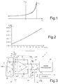
- Figure 1 also shows with a dashed line the plot of the junction capacitance determined using more accurate calculations.
- the junction capacitance C j in temperature ranges wherein integrated circuits normally operate, the junction capacitance C j has an approximately linear plot as a function of temperature. Consequently, to a first approximation, the reading of the junction capacitance C j of a reverse biased PN diode has a relation of direct proportionality with the local temperature, and reading of the junction capacitance and/or of its variation supplies direct information on the temperature or on the temperature variation.
- FIG. 3 shows a temperature sensor 1 that exploits the principle explained above.
- the temperature sensor 1 comprises a sensor input 2 supplied with a sensor excitation signal, i.e., the timed biasing voltage DRH.
- a sensing diode 3, of a PN-junction type has its cathode coupled to the sensor input 2 and its anode coupled to an inverting input 7 of an operational amplifier 4.
- a reference capacitor 5, having a reference capacitance C R is coupled between the sensor input 2 and a non-inverting input 8 of the operational amplifier 4.
- the reference capacitance C R is chosen so as to have the same value as the junction capacitance C j at room temperature.
- the inputs 7, 8 of the operational amplifier 4 are both coupled to a first reference potential line 10, set at a first common mode potential V CMin , through a respective input switch 11.
- the input switches 11 are controlled by a same reset signal R.
- the operational amplifier 4 is of a fully differential type, has a pair of outputs 15, 16 and has a capacitive feedback formed by a first and a second feedback capacitors 17, 18, which have the same feedback capacitance C i .
- the first feedback capacitor 17 is coupled between the first output 15 and the inverting input 7
- the second feedback capacitor 18 is coupled between the second output 16 and the non-inverting input 8 of the operational amplifier 4.
- the outputs 15, 16 of the operational amplifier 4 are further coupled to a second reference potential line 20, set at a second common mode potential V CMout , through a respective output switch 21.
- the output switches 21 are controlled by the reset signal R.
- a timed biasing voltage DRH is supplied on the input 2 and switches between a low value (for example, 0.625 V) and a high value V DRH (for example, 1.25V).
- the low value is in any case positive for keeping the sensing diode 3 (which has its anode coupled to the virtual ground on the inverting input 7 of the operational amplifier 4) reverse biased in all the sensing phases, and the high value is chosen for generating a voltage step ⁇ V of a preset value, as explained in detail hereinafter.
- the sensing diode 3 and the reference capacitor 5 form a sensing element 25 and the operational amplifier 4, with the capacitive feedback, forms a switched capacitor differential amplifier stage of a known type and widely used, for example, in reading of MEMS structures.
- the operational amplifier 4 and the relevant feedback network 17, 18, 11, 21 may be incorporated in an ASIC (Application Specific Integrated Circuit) 28.
- ASIC Application Specific Integrated Circuit
- the sensing diode 3 and the reference capacitor 5 may be formed in a semiconductor material chip, as described in greater detail with reference to Figure 8 .
- the outputs 15 and 16 of the operational amplifier 4 are coupled to a processing stage 30, generally external to the temperature sensor 1 but possibly also integrated in the ASIC.
- the processing stage 30 may comprise circuits for amplification of the output voltage V o and for analog-to-digital conversion.
- a timing stage 31 generates biasing/timing signals for the temperature sensor 1 and for the processing stage 30, such as the reset signal R, the timed biasing voltage DRH, and a reading acquisition signal S for the processing stage 30.
- the reset signal R and the reading acquisition signal S have the same period, but different duty cycle.
- the sensing period T 2 is considered as being divided into two half periods T 11 and T 12 , corresponding to two successive periods of the acquisition period T 1 .
- the reset signal R switches to the high state, causing the input switches 11 and of the output switches 21 to switch off. Consequently, the inputs 7, 8 of the operational amplifier 4 are coupled to the first common mode potential V cMin (for example, 0.625 V, i.e., to the low value of the timed biasing voltage DRH), and the outputs 15, 16 of the operational amplifier 4 are coupled to the second common mode potential V cMout (for example, 1 V), thus resetting the operational amplifier 4.
- V cMin for example, 0.625 V, i.e., to the low value of the timed biasing voltage DRH
- V cMout for example, 1 V
- the timed biasing voltage DRH (for example, 0.625 V) is low, as likewise the reading acquisition signal S.
- the output voltage V o is thus not acquired by the signal processing stage 30.
- the reset signal R switches to the low state, causing opening of the input and output switches 11, 21 and causing the input nodes 7, 8 and output nodes 15, 16 of the operational amplifier 4 to be independent.
- the timed biasing voltage DRH is low, as the reading acquisition signal S.
- the step t 1 -t 2 may be adopted in case of use of the correlated double sampling (CDS) technique.
- CDS correlated double sampling
- offset sampling is carried out, which may then be subtracted during the sensing phase. In this way, it is possible to reduce the offset.
- the timed biasing voltage DRH has a rising edge and reaches a value that reverse biases the sensing diode 3, for example, at 1.25 V. In this condition, neglecting possible losses, a reverse current flows in the sensing diode 3. Further, a reference current flows in the reference capacitor 5.
- This step terminates at instant t 3 , where a new period T 1 of the reading acquisition signal S and of the reset signal R and the second half period T 12 of the sensing signal DRH start.
- the reset signal R switches to high, and the reading acquisition signal S switches to low.
- the operational amplifier 4 is thus reset again, in a way generally similar to what described for the reset phase of the first half period T 11 , with the only difference that, now, the timed biasing voltage DRH is high. This value does not, however, affect the reset phase since, as before, the operational amplifier 4 is reset, and the output voltage V o is not acquired by the signal processing stage 30.
- the timed biasing voltage DRH has a falling edge, thus causing a charge displacement opposite to that of the sensing phase in the first half period. Consequently, the output voltage V o has a value V o t ⁇ ⁇ C C i ⁇ V with a opposite sign to Eq. (5), since in this half period T 12 the step ⁇ V of the timed biasing voltage DRH is a down step and is equal to -V DRH .
- the value of the output voltage V o is acquired from the signal processing stage 30 thanks to the high value of the reading acquisition signal S.
- the signal processing stage 30 thus modifies the sign of the output voltage V o in one of the two half periods T 11 and T 12 , in a way synchronised with the sensing period T 2 .
- This step terminates at instant t 3 , where a new period T 1 of the reading acquisition signal S and of the reset signal R starts, as well as a new period T 2 of the sensing signal DRH.
- the sensing diode 3 intrinsically presents a current leakage that, in some situations, may reduce reading precision in an undesirable way.
- the aforesaid current leakage of the sensing diode 3 determines a variation of the charge Q 1 .
- the sensing diode 3 undergoes a displacement of charge equal to Q 1 - Q L , where Q L is the charge due to the leakage current.
- a more precise approximation of the output voltage V o is thus the following: V o t ⁇ ⁇ C C i ⁇ V + I L ⁇ C i ⁇ T 1 2 where I L is the leakage current of the sensing diode 3.
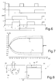
- Figure 5 shows an embodiment wherein the leakage current I L of the sensing diode 3 is compensated.
- the temperature sensor of Figure 5 has the same basic structure as the temperature sensor of Figure 3 , where a compensation diode 40 and a symmetry capacitor 41, having a capacitance equal to the capacitance C R of the reference capacitor 5, have been added.
- the elements in common with those of Figure 3 are thus designated by the same reference numbers.
- the compensation diode 40 has its anode coupled to the non-inverting input 8 of the operational amplifier 4 and its cathode coupled to a third reference potential line 43, set at a non-constant biasing potential V STB , and the symmetry capacitor 41 is coupled between the inverting input 7 of the operational amplifier 4 and the third reference potential line 43.
- the biasing potential V STB switches between two positive values, for example between 0 V and 2.5 V, to be surely higher than the potential on the inputs 7 and 8 of the operational amplifier 4 and keep the compensation diode 40 reverse biased.
- Two current generators 45 are also illustrated in Figure 5 and represent the leakage currents I L of the sensing diode 3 and of the compensation diode 40.
- the sensing diode 3, the reference capacitor 5, the compensation diode 40, and the symmetry capacitor 41 form a capacitive bridge 44.
- the biasing potential V STB has the same sign as the timed biasing voltage DRH during the sensing phase; namely, it is positive with respect to the virtual ground on the inputs 7 and 8 of the operational amplifier 4 for keeping the compensation diode 40 reverse biased in all the sensing phases and to have a voltage step ⁇ V equal to the step of the sensing signal DHR in order to keep the compensation diode 40 in the same operating conditions as the sensing diode 3.
- the feedback capacitors 17 and 18 are traversed by the following currents:
- V o of the temperature sensor of Figure 5 may be expressed as follows: V o t ⁇ ⁇ C C i ⁇ V + I L 1 ⁇ C i ⁇ T 1 2 - I L 2 ⁇ C i ⁇ T 1 2
- the compensation diode 40 By manufacturing the compensation diode 40 in the same way and with the same parameters as the sensing diode 3, due also to the same reverse biasing of the diodes 3 and 40, they generate leakage currents I L1 and I L2 that are the same so that in Eq. (8) the two contributions of the leakage currents I L1 and I L2 cancel out, and the output voltage V o may be expressed again by Eq. (6).
- the output voltage V o of the operational amplifier 4 without compensation has a reading error proportional both to the leakage current and to the integration time. Instead, the output voltage V o with compensation, after a transient, is insensitive to the above parameters.
- Figure 8 shows a possible implementation of the compensation diode 3 and of the symmetry capacitor 5.
- the temperature sensor 1 is formed in a chip 60 of semiconductor material, such as silicon, having a substrate 50 of a P type, accommodates a well 51 of an N type, which forms the cathode K of the compensation diode 3.
- the well 51 in turn accommodates a tap 52, of a P type, forming the anode A of the compensation diode 3.
- An insulating layer 55 extends over the substrate 50 and accommodates two metal regions 56, 57, arranged on top of each other and formed, for example, in two different metallization levels of the chip 60.
- the metal regions 56, 57 form, together with the portion of the insulating layer 55 arranged in between, the reference capacitor 5.
- the compensation diode 40 and the symmetry capacitor 41 may be formed in a similar way.
- the described temperature sensor comprises only a few simple components of a capacitive type (sensing diode 3, reference capacitor 5, possibly a capacitive bridge 44) that may easily be integrated and require only a small area, which cooperate with a sensing network (operational amplifier 4 and corresponding feedback network) that may be manufactured using standard CMOS technology.
- the sensor has a zero d.c. biasing voltage, and thus a low current consumption.
- the temperature sensor 1 may be compensated with respect to the current leakages by a few simple components (compensation diode 40, symmetry capacitor 41), thus supplying a particularly precise output.
- the switched capacitor differential amplifier 26 may be replaced by another type of sensing circuit, and/or be formed in a different way from what illustrated, for example be formed as a non-fully differential amplifier.
Landscapes
- Physics & Mathematics (AREA)
- General Physics & Mathematics (AREA)
- Engineering & Computer Science (AREA)
- Power Engineering (AREA)
- Measuring Temperature Or Quantity Of Heat (AREA)
- Semiconductor Integrated Circuits (AREA)
- Amplifiers (AREA)
Applications Claiming Priority (1)
| Application Number | Priority Date | Filing Date | Title |
|---|---|---|---|
| ITTO20150189 | 2015-03-30 |
Publications (2)
| Publication Number | Publication Date |
|---|---|
| EP3076143A1 true EP3076143A1 (de) | 2016-10-05 |
| EP3076143B1 EP3076143B1 (de) | 2018-06-13 |
Family
ID=53189985
Family Applications (1)
| Application Number | Title | Priority Date | Filing Date |
|---|---|---|---|
| EP15200458.6A Active EP3076143B1 (de) | 2015-03-30 | 2015-12-16 | Integrierte elektronische vorrichtung mit temperatursensor und messverfahren |
Country Status (3)
| Country | Link |
|---|---|
| US (3) | US10317293B2 (de) |
| EP (1) | EP3076143B1 (de) |
| CN (2) | CN106017710B (de) |
Families Citing this family (14)
| Publication number | Priority date | Publication date | Assignee | Title |
|---|---|---|---|---|
| US9182295B1 (en) * | 2011-09-09 | 2015-11-10 | Sitime Corporation | Circuitry and techniques for resistor-based temperature sensing |
| CN106017710B (zh) * | 2015-03-30 | 2020-01-07 | 意法半导体股份有限公司 | 包含温度传感器的集成电子器件和感测方法 |
| CN106441614A (zh) * | 2016-09-14 | 2017-02-22 | 成都百奥诺维生物科技有限公司 | 一种水解法提取鱼皮胶原蛋白用高精度温度监测系统 |
| CN106441615A (zh) * | 2016-09-14 | 2017-02-22 | 成都百奥诺维生物科技有限公司 | 基于偏置电路的水解法提取鱼皮胶原蛋白用温度监测系统 |
| DE102017100264A1 (de) * | 2017-01-09 | 2018-07-12 | Endress + Hauser Wetzer Gmbh + Co. Kg | Vorrichtung und Verfahren zur in situ Kalibrierung eines Thermometers |
| CN107144778A (zh) * | 2017-05-16 | 2017-09-08 | 珠海格力节能环保制冷技术研究中心有限公司 | 一种芯片温度检测装置及方法 |
| US10578497B2 (en) | 2017-09-17 | 2020-03-03 | Qualcomm Incorporated | Diode-based temperature sensor |
| US11428702B2 (en) * | 2018-08-14 | 2022-08-30 | Invensense, Inc. | Applying a positive feedback voltage to an electromechanical sensor utilizing a voltage-to-voltage converter to facilitate a reduction of charge flow in such sensor representing spring |
| CN111550835B (zh) * | 2019-02-12 | 2024-06-28 | 陈景超 | 一种带有测温电路的加热装置及其控制方法 |
| JP7146668B2 (ja) * | 2019-02-21 | 2022-10-04 | ラピスセミコンダクタ株式会社 | 容量センサ回路及び半導体集積回路 |
| CN113156159B (zh) * | 2021-02-10 | 2022-08-19 | 复旦大学 | 一种应用于飞行器的无空速管的空速计 |
| US11908530B2 (en) * | 2021-10-08 | 2024-02-20 | Micron Technology, Inc. | Multi-sampled, charge-sharing thermometer in memory device |
| CN115437447B (zh) * | 2022-10-26 | 2023-08-01 | 电子科技大学 | 一种带低温漏电补偿的mos管温度传感器 |
| CN116337497B (zh) * | 2023-03-10 | 2025-07-25 | 苏州浪潮智能科技有限公司 | 一种未封装cpu的发热模拟冶具及散热测试方法 |
Citations (2)
| Publication number | Priority date | Publication date | Assignee | Title |
|---|---|---|---|---|
| EP1887333A1 (de) * | 2006-08-04 | 2008-02-13 | STMicroelectronics Design and Application S.R.O. | Mikroelektronische Schaltung ausgestattet mit einer thermischen Schutzschaltung und thermische Schutzmethode für eine mikroelektronische Schaltung |
| US20120257650A1 (en) * | 2011-04-08 | 2012-10-11 | Chowdhury Golam R | On-chip temperature sensor |
Family Cites Families (10)
| Publication number | Priority date | Publication date | Assignee | Title |
|---|---|---|---|---|
| US5757008A (en) * | 1995-11-08 | 1998-05-26 | Nikon Corporation | Infrared-ray image sensor |
| JP4620889B2 (ja) * | 2001-03-22 | 2011-01-26 | 三菱電機株式会社 | 電力用半導体装置 |
| JP3790704B2 (ja) * | 2001-12-18 | 2006-06-28 | 三菱電機株式会社 | 高周波信号用トランジスタの位相調整回路、及び、半導体集積回路 |
| US7083328B2 (en) * | 2004-08-05 | 2006-08-01 | Texas Instruments Incorporated | Remote diode temperature sense method with parasitic resistance cancellation |
| JP4550726B2 (ja) * | 2005-12-01 | 2010-09-22 | 三菱電機株式会社 | 電圧制御発振器 |
| DE602007002805D1 (de) * | 2006-04-20 | 2009-11-26 | Nxp Bv | Verfahren und vorrichtung zur bestimmung der temperatur eines halbleitersubstrats |
| US8063757B2 (en) * | 2007-07-18 | 2011-11-22 | Tesla Motors, Inc. | Charge state indicator for an electric vehicle |
| US8092080B2 (en) | 2008-08-15 | 2012-01-10 | Siemens Energy, Inc. | Wireless telemetry circuit structure for measuring temperature in high temperature environments |
| US9728580B2 (en) * | 2013-05-13 | 2017-08-08 | Infineon Technologies Ag | Power transistor with integrated temperature sensor element, power transistor circuit, method for operating a power transistor, and method for operating a power transistor circuit |
| CN106017710B (zh) * | 2015-03-30 | 2020-01-07 | 意法半导体股份有限公司 | 包含温度传感器的集成电子器件和感测方法 |
-
2015
- 2015-11-18 CN CN201510796627.7A patent/CN106017710B/zh active Active
- 2015-11-18 CN CN201520922001.1U patent/CN205175565U/zh not_active Withdrawn - After Issue
- 2015-12-03 US US14/958,786 patent/US10317293B2/en active Active
- 2015-12-16 EP EP15200458.6A patent/EP3076143B1/de active Active
-
2019
- 2019-04-25 US US16/394,804 patent/US10739212B2/en active Active
-
2020
- 2020-07-06 US US16/921,819 patent/US11035739B2/en active Active
Patent Citations (2)
| Publication number | Priority date | Publication date | Assignee | Title |
|---|---|---|---|---|
| EP1887333A1 (de) * | 2006-08-04 | 2008-02-13 | STMicroelectronics Design and Application S.R.O. | Mikroelektronische Schaltung ausgestattet mit einer thermischen Schutzschaltung und thermische Schutzmethode für eine mikroelektronische Schaltung |
| US20120257650A1 (en) * | 2011-04-08 | 2012-10-11 | Chowdhury Golam R | On-chip temperature sensor |
Non-Patent Citations (3)
| Title |
|---|
| CHUN-HUA CAI; MING QIN: "High-performance bulk silicon interdigital capacitive temperature sensor based on graphene oxide", ELECTRONICS LETTERS, vol. 49, no. 7, 28 March 2013 (2013-03-28) |
| HONG-YU MA; QING-AN HUANG; MING QIN; TINGTING LU: "Micromachined Silicon Capacitive Temperature Sensor for Radiosonde Applications", 2009, IEEE |
| TUTHILL M: "A SWITCHED-CURRENT, SWITCHED-CAPACITOR TEMPERATURE SENSOR IN 0.6-MUM CMOS", IEEE JOURNAL OF SOLID-STATE CIRCUITS, IEEE SERVICE CENTER, PISCATAWAY, NJ, USA, vol. 33, no. 7, 1 July 1998 (1998-07-01), pages 1117 - 1122, XP000849171, ISSN: 0018-9200, DOI: 10.1109/4.701277 * |
Also Published As
| Publication number | Publication date |
|---|---|
| US20160290875A1 (en) | 2016-10-06 |
| CN205175565U (zh) | 2016-04-20 |
| EP3076143B1 (de) | 2018-06-13 |
| US10317293B2 (en) | 2019-06-11 |
| CN106017710B (zh) | 2020-01-07 |
| US11035739B2 (en) | 2021-06-15 |
| US10739212B2 (en) | 2020-08-11 |
| CN106017710A (zh) | 2016-10-12 |
| US20200333197A1 (en) | 2020-10-22 |
| US20190250047A1 (en) | 2019-08-15 |
Similar Documents
| Publication | Publication Date | Title |
|---|---|---|
| US11035739B2 (en) | Integrated electronic device comprising a temperature sensor and sensing method | |
| US9785176B2 (en) | Small-circuit-scale reference voltage generating circuit | |
| US10254176B2 (en) | Strain-insensitive temperature sensor | |
| US6014042A (en) | Phase detector using switched capacitors | |
| US20070252573A1 (en) | Reference voltage generator circuit | |
| EP2295944A2 (de) | Temperatursensor | |
| CN107490394A (zh) | 开关电阻器传感器电桥、对应的系统和方法 | |
| US7145380B2 (en) | Low power consumed and small circuit area occupied temperature sensor | |
| US20110018616A1 (en) | Charge pump circuit | |
| US11237065B2 (en) | High dynamic range temperature sensor | |
| US20100066582A1 (en) | Current mode double-integration conversion apparatus | |
| US10914618B2 (en) | Readout circuit for sensor and readout method thereof | |
| US6639414B2 (en) | Circuit for measuring changes in capacitor gap using a switched capacitor technique | |
| CN111307314B (zh) | 一种用于检测半导体芯片温度的电路及方法 | |
| CN107817060B (zh) | 温度数字转换器 | |
| Bruschi et al. | A low-power capacitance to pulse width converter for MEMS interfacing | |
| CN115378434A (zh) | 一种用于温度传感器的电压-脉宽转换电路及温度传感器 | |
| JP2009058290A (ja) | チャージアンプ、チャージアンプ装置、及び、バイアス電流補償方法 | |
| Schoeneberg et al. | A novel readout technique for capacitive gas sensors | |
| KR20160108207A (ko) | 비교 회로 및 센서 장치 | |
| JP4498507B2 (ja) | 差動増幅回路および高温用増幅回路 | |
| Mizushima et al. | A high-accuracy capacitance-to-voltage converter for capacitive sensors | |
| EP4365563B1 (de) | Temperatursensor und schaltung | |
| Falconi et al. | Low voltage, low power, compact, high accuracy, high precision PTAT temperature sensor for deep sub-micron CMOS systems | |
| Lu et al. | A wide-range capacitance-to-frequency readout circuit using pulse-width detection and delay-line-based feedback control loop |
Legal Events
| Date | Code | Title | Description |
|---|---|---|---|
| PUAI | Public reference made under article 153(3) epc to a published international application that has entered the european phase |
Free format text: ORIGINAL CODE: 0009012 |
|
| AK | Designated contracting states |
Kind code of ref document: A1 Designated state(s): AL AT BE BG CH CY CZ DE DK EE ES FI FR GB GR HR HU IE IS IT LI LT LU LV MC MK MT NL NO PL PT RO RS SE SI SK SM TR |
|
| AX | Request for extension of the european patent |
Extension state: BA ME |
|
| 17P | Request for examination filed |
Effective date: 20170404 |
|
| RBV | Designated contracting states (corrected) |
Designated state(s): AL AT BE BG CH CY CZ DE DK EE ES FI FR GB GR HR HU IE IS IT LI LT LU LV MC MK MT NL NO PL PT RO RS SE SI SK SM TR |
|
| GRAP | Despatch of communication of intention to grant a patent |
Free format text: ORIGINAL CODE: EPIDOSNIGR1 |
|
| INTG | Intention to grant announced |
Effective date: 20180103 |
|
| GRAS | Grant fee paid |
Free format text: ORIGINAL CODE: EPIDOSNIGR3 |
|
| GRAA | (expected) grant |
Free format text: ORIGINAL CODE: 0009210 |
|
| AK | Designated contracting states |
Kind code of ref document: B1 Designated state(s): AL AT BE BG CH CY CZ DE DK EE ES FI FR GB GR HR HU IE IS IT LI LT LU LV MC MK MT NL NO PL PT RO RS SE SI SK SM TR |
|
| REG | Reference to a national code |
Ref country code: GB Ref legal event code: FG4D |
|
| REG | Reference to a national code |
Ref country code: CH Ref legal event code: EP Ref country code: AT Ref legal event code: REF Ref document number: 1008977 Country of ref document: AT Kind code of ref document: T Effective date: 20180615 |
|
| REG | Reference to a national code |
Ref country code: IE Ref legal event code: FG4D |
|
| REG | Reference to a national code |
Ref country code: DE Ref legal event code: R096 Ref document number: 602015012189 Country of ref document: DE |
|
| REG | Reference to a national code |
Ref country code: NL Ref legal event code: MP Effective date: 20180613 |
|
| REG | Reference to a national code |
Ref country code: LT Ref legal event code: MG4D |
|
| PG25 | Lapsed in a contracting state [announced via postgrant information from national office to epo] |
Ref country code: LT Free format text: LAPSE BECAUSE OF FAILURE TO SUBMIT A TRANSLATION OF THE DESCRIPTION OR TO PAY THE FEE WITHIN THE PRESCRIBED TIME-LIMIT Effective date: 20180613 Ref country code: CY Free format text: LAPSE BECAUSE OF FAILURE TO SUBMIT A TRANSLATION OF THE DESCRIPTION OR TO PAY THE FEE WITHIN THE PRESCRIBED TIME-LIMIT Effective date: 20180613 Ref country code: ES Free format text: LAPSE BECAUSE OF FAILURE TO SUBMIT A TRANSLATION OF THE DESCRIPTION OR TO PAY THE FEE WITHIN THE PRESCRIBED TIME-LIMIT Effective date: 20180613 Ref country code: BG Free format text: LAPSE BECAUSE OF FAILURE TO SUBMIT A TRANSLATION OF THE DESCRIPTION OR TO PAY THE FEE WITHIN THE PRESCRIBED TIME-LIMIT Effective date: 20180913 Ref country code: FI Free format text: LAPSE BECAUSE OF FAILURE TO SUBMIT A TRANSLATION OF THE DESCRIPTION OR TO PAY THE FEE WITHIN THE PRESCRIBED TIME-LIMIT Effective date: 20180613 Ref country code: NO Free format text: LAPSE BECAUSE OF FAILURE TO SUBMIT A TRANSLATION OF THE DESCRIPTION OR TO PAY THE FEE WITHIN THE PRESCRIBED TIME-LIMIT Effective date: 20180913 Ref country code: SE Free format text: LAPSE BECAUSE OF FAILURE TO SUBMIT A TRANSLATION OF THE DESCRIPTION OR TO PAY THE FEE WITHIN THE PRESCRIBED TIME-LIMIT Effective date: 20180613 |
|
| PG25 | Lapsed in a contracting state [announced via postgrant information from national office to epo] |
Ref country code: LV Free format text: LAPSE BECAUSE OF FAILURE TO SUBMIT A TRANSLATION OF THE DESCRIPTION OR TO PAY THE FEE WITHIN THE PRESCRIBED TIME-LIMIT Effective date: 20180613 Ref country code: RS Free format text: LAPSE BECAUSE OF FAILURE TO SUBMIT A TRANSLATION OF THE DESCRIPTION OR TO PAY THE FEE WITHIN THE PRESCRIBED TIME-LIMIT Effective date: 20180613 Ref country code: GR Free format text: LAPSE BECAUSE OF FAILURE TO SUBMIT A TRANSLATION OF THE DESCRIPTION OR TO PAY THE FEE WITHIN THE PRESCRIBED TIME-LIMIT Effective date: 20180914 Ref country code: HR Free format text: LAPSE BECAUSE OF FAILURE TO SUBMIT A TRANSLATION OF THE DESCRIPTION OR TO PAY THE FEE WITHIN THE PRESCRIBED TIME-LIMIT Effective date: 20180613 |
|
| REG | Reference to a national code |
Ref country code: AT Ref legal event code: MK05 Ref document number: 1008977 Country of ref document: AT Kind code of ref document: T Effective date: 20180613 |
|
| PG25 | Lapsed in a contracting state [announced via postgrant information from national office to epo] |
Ref country code: NL Free format text: LAPSE BECAUSE OF FAILURE TO SUBMIT A TRANSLATION OF THE DESCRIPTION OR TO PAY THE FEE WITHIN THE PRESCRIBED TIME-LIMIT Effective date: 20180613 |
|
| PG25 | Lapsed in a contracting state [announced via postgrant information from national office to epo] |
Ref country code: PL Free format text: LAPSE BECAUSE OF FAILURE TO SUBMIT A TRANSLATION OF THE DESCRIPTION OR TO PAY THE FEE WITHIN THE PRESCRIBED TIME-LIMIT Effective date: 20180613 Ref country code: SK Free format text: LAPSE BECAUSE OF FAILURE TO SUBMIT A TRANSLATION OF THE DESCRIPTION OR TO PAY THE FEE WITHIN THE PRESCRIBED TIME-LIMIT Effective date: 20180613 Ref country code: RO Free format text: LAPSE BECAUSE OF FAILURE TO SUBMIT A TRANSLATION OF THE DESCRIPTION OR TO PAY THE FEE WITHIN THE PRESCRIBED TIME-LIMIT Effective date: 20180613 Ref country code: CZ Free format text: LAPSE BECAUSE OF FAILURE TO SUBMIT A TRANSLATION OF THE DESCRIPTION OR TO PAY THE FEE WITHIN THE PRESCRIBED TIME-LIMIT Effective date: 20180613 Ref country code: EE Free format text: LAPSE BECAUSE OF FAILURE TO SUBMIT A TRANSLATION OF THE DESCRIPTION OR TO PAY THE FEE WITHIN THE PRESCRIBED TIME-LIMIT Effective date: 20180613 Ref country code: AT Free format text: LAPSE BECAUSE OF FAILURE TO SUBMIT A TRANSLATION OF THE DESCRIPTION OR TO PAY THE FEE WITHIN THE PRESCRIBED TIME-LIMIT Effective date: 20180613 Ref country code: IS Free format text: LAPSE BECAUSE OF FAILURE TO SUBMIT A TRANSLATION OF THE DESCRIPTION OR TO PAY THE FEE WITHIN THE PRESCRIBED TIME-LIMIT Effective date: 20181013 |
|
| PG25 | Lapsed in a contracting state [announced via postgrant information from national office to epo] |
Ref country code: SM Free format text: LAPSE BECAUSE OF FAILURE TO SUBMIT A TRANSLATION OF THE DESCRIPTION OR TO PAY THE FEE WITHIN THE PRESCRIBED TIME-LIMIT Effective date: 20180613 Ref country code: IT Free format text: LAPSE BECAUSE OF FAILURE TO SUBMIT A TRANSLATION OF THE DESCRIPTION OR TO PAY THE FEE WITHIN THE PRESCRIBED TIME-LIMIT Effective date: 20180613 |
|
| REG | Reference to a national code |
Ref country code: DE Ref legal event code: R097 Ref document number: 602015012189 Country of ref document: DE |
|
| PLBE | No opposition filed within time limit |
Free format text: ORIGINAL CODE: 0009261 |
|
| STAA | Information on the status of an ep patent application or granted ep patent |
Free format text: STATUS: NO OPPOSITION FILED WITHIN TIME LIMIT |
|
| 26N | No opposition filed |
Effective date: 20190314 |
|
| PG25 | Lapsed in a contracting state [announced via postgrant information from national office to epo] |
Ref country code: SI Free format text: LAPSE BECAUSE OF FAILURE TO SUBMIT A TRANSLATION OF THE DESCRIPTION OR TO PAY THE FEE WITHIN THE PRESCRIBED TIME-LIMIT Effective date: 20180613 Ref country code: DK Free format text: LAPSE BECAUSE OF FAILURE TO SUBMIT A TRANSLATION OF THE DESCRIPTION OR TO PAY THE FEE WITHIN THE PRESCRIBED TIME-LIMIT Effective date: 20180613 |
|
| REG | Reference to a national code |
Ref country code: CH Ref legal event code: PL |
|
| PG25 | Lapsed in a contracting state [announced via postgrant information from national office to epo] |
Ref country code: LU Free format text: LAPSE BECAUSE OF NON-PAYMENT OF DUE FEES Effective date: 20181216 Ref country code: MC Free format text: LAPSE BECAUSE OF FAILURE TO SUBMIT A TRANSLATION OF THE DESCRIPTION OR TO PAY THE FEE WITHIN THE PRESCRIBED TIME-LIMIT Effective date: 20180613 |
|
| REG | Reference to a national code |
Ref country code: IE Ref legal event code: MM4A |
|
| REG | Reference to a national code |
Ref country code: BE Ref legal event code: MM Effective date: 20181231 |
|
| PG25 | Lapsed in a contracting state [announced via postgrant information from national office to epo] |
Ref country code: IE Free format text: LAPSE BECAUSE OF NON-PAYMENT OF DUE FEES Effective date: 20181216 Ref country code: FR Free format text: LAPSE BECAUSE OF NON-PAYMENT OF DUE FEES Effective date: 20181231 |
|
| PG25 | Lapsed in a contracting state [announced via postgrant information from national office to epo] |
Ref country code: AL Free format text: LAPSE BECAUSE OF FAILURE TO SUBMIT A TRANSLATION OF THE DESCRIPTION OR TO PAY THE FEE WITHIN THE PRESCRIBED TIME-LIMIT Effective date: 20180613 Ref country code: BE Free format text: LAPSE BECAUSE OF NON-PAYMENT OF DUE FEES Effective date: 20181231 |
|
| PG25 | Lapsed in a contracting state [announced via postgrant information from national office to epo] |
Ref country code: CH Free format text: LAPSE BECAUSE OF NON-PAYMENT OF DUE FEES Effective date: 20181231 Ref country code: LI Free format text: LAPSE BECAUSE OF NON-PAYMENT OF DUE FEES Effective date: 20181231 |
|
| PG25 | Lapsed in a contracting state [announced via postgrant information from national office to epo] |
Ref country code: MT Free format text: LAPSE BECAUSE OF NON-PAYMENT OF DUE FEES Effective date: 20181216 |
|
| PG25 | Lapsed in a contracting state [announced via postgrant information from national office to epo] |
Ref country code: TR Free format text: LAPSE BECAUSE OF FAILURE TO SUBMIT A TRANSLATION OF THE DESCRIPTION OR TO PAY THE FEE WITHIN THE PRESCRIBED TIME-LIMIT Effective date: 20180613 |
|
| PG25 | Lapsed in a contracting state [announced via postgrant information from national office to epo] |
Ref country code: PT Free format text: LAPSE BECAUSE OF FAILURE TO SUBMIT A TRANSLATION OF THE DESCRIPTION OR TO PAY THE FEE WITHIN THE PRESCRIBED TIME-LIMIT Effective date: 20180613 |
|
| PG25 | Lapsed in a contracting state [announced via postgrant information from national office to epo] |
Ref country code: HU Free format text: LAPSE BECAUSE OF FAILURE TO SUBMIT A TRANSLATION OF THE DESCRIPTION OR TO PAY THE FEE WITHIN THE PRESCRIBED TIME-LIMIT; INVALID AB INITIO Effective date: 20151216 Ref country code: MK Free format text: LAPSE BECAUSE OF NON-PAYMENT OF DUE FEES Effective date: 20180613 |
|
| GBPC | Gb: european patent ceased through non-payment of renewal fee |
Effective date: 20191216 |
|
| PG25 | Lapsed in a contracting state [announced via postgrant information from national office to epo] |
Ref country code: GB Free format text: LAPSE BECAUSE OF NON-PAYMENT OF DUE FEES Effective date: 20191216 |
|
| PGFP | Annual fee paid to national office [announced via postgrant information from national office to epo] |
Ref country code: DE Payment date: 20251126 Year of fee payment: 11 |