EP3076429B1 - Ensemble de boîtier de semi-conducteur avec une capacité de type mlcc ou chip-cap incorporé - Google Patents
Ensemble de boîtier de semi-conducteur avec une capacité de type mlcc ou chip-cap incorporé Download PDFInfo
- Publication number
- EP3076429B1 EP3076429B1 EP16160070.5A EP16160070A EP3076429B1 EP 3076429 B1 EP3076429 B1 EP 3076429B1 EP 16160070 A EP16160070 A EP 16160070A EP 3076429 B1 EP3076429 B1 EP 3076429B1
- Authority
- EP
- European Patent Office
- Prior art keywords
- semiconductor package
- rdl structure
- semiconductor
- semiconductor die
- package assembly
- Prior art date
- Legal status (The legal status is an assumption and is not a legal conclusion. Google has not performed a legal analysis and makes no representation as to the accuracy of the status listed.)
- Active
Links
Images



Classifications
-
- H—ELECTRICITY
- H10—SEMICONDUCTOR DEVICES; ELECTRIC SOLID-STATE DEVICES NOT OTHERWISE PROVIDED FOR
- H10W—GENERIC PACKAGES, INTERCONNECTIONS, CONNECTORS OR OTHER CONSTRUCTIONAL DETAILS OF DEVICES COVERED BY CLASS H10
- H10W72/00—Interconnections or connectors in packages
-
- H—ELECTRICITY
- H10—SEMICONDUCTOR DEVICES; ELECTRIC SOLID-STATE DEVICES NOT OTHERWISE PROVIDED FOR
- H10W—GENERIC PACKAGES, INTERCONNECTIONS, CONNECTORS OR OTHER CONSTRUCTIONAL DETAILS OF DEVICES COVERED BY CLASS H10
- H10W70/00—Package substrates; Interposers; Redistribution layers [RDL]
- H10W70/01—Manufacture or treatment
- H10W70/05—Manufacture or treatment of insulating or insulated package substrates, or of interposers, or of redistribution layers
- H10W70/08—Manufacture or treatment of insulating or insulated package substrates, or of interposers, or of redistribution layers by depositing layers on the chip or wafer, e.g. "chip-first" RDLs
- H10W70/09—Manufacture or treatment of insulating or insulated package substrates, or of interposers, or of redistribution layers by depositing layers on the chip or wafer, e.g. "chip-first" RDLs extending onto an encapsulation that laterally surrounds the chip or wafer, e.g. fan-out wafer level package [FOWLP] RDLs
-
- H—ELECTRICITY
- H10—SEMICONDUCTOR DEVICES; ELECTRIC SOLID-STATE DEVICES NOT OTHERWISE PROVIDED FOR
- H10W—GENERIC PACKAGES, INTERCONNECTIONS, CONNECTORS OR OTHER CONSTRUCTIONAL DETAILS OF DEVICES COVERED BY CLASS H10
- H10W70/00—Package substrates; Interposers; Redistribution layers [RDL]
- H10W70/60—Insulating or insulated package substrates; Interposers; Redistribution layers
-
- H—ELECTRICITY
- H10—SEMICONDUCTOR DEVICES; ELECTRIC SOLID-STATE DEVICES NOT OTHERWISE PROVIDED FOR
- H10W—GENERIC PACKAGES, INTERCONNECTIONS, CONNECTORS OR OTHER CONSTRUCTIONAL DETAILS OF DEVICES COVERED BY CLASS H10
- H10W70/00—Package substrates; Interposers; Redistribution layers [RDL]
- H10W70/60—Insulating or insulated package substrates; Interposers; Redistribution layers
- H10W70/611—Insulating or insulated package substrates; Interposers; Redistribution layers for connecting multiple chips together
- H10W70/614—Insulating or insulated package substrates; Interposers; Redistribution layers for connecting multiple chips together the multiple chips being integrally enclosed
-
- H—ELECTRICITY
- H10—SEMICONDUCTOR DEVICES; ELECTRIC SOLID-STATE DEVICES NOT OTHERWISE PROVIDED FOR
- H10W—GENERIC PACKAGES, INTERCONNECTIONS, CONNECTORS OR OTHER CONSTRUCTIONAL DETAILS OF DEVICES COVERED BY CLASS H10
- H10W70/00—Package substrates; Interposers; Redistribution layers [RDL]
- H10W70/60—Insulating or insulated package substrates; Interposers; Redistribution layers
- H10W70/62—Insulating or insulated package substrates; Interposers; Redistribution layers characterised by their interconnections
- H10W70/63—Vias, e.g. via plugs
- H10W70/635—Through-vias
-
- H—ELECTRICITY
- H10—SEMICONDUCTOR DEVICES; ELECTRIC SOLID-STATE DEVICES NOT OTHERWISE PROVIDED FOR
- H10W—GENERIC PACKAGES, INTERCONNECTIONS, CONNECTORS OR OTHER CONSTRUCTIONAL DETAILS OF DEVICES COVERED BY CLASS H10
- H10W70/00—Package substrates; Interposers; Redistribution layers [RDL]
- H10W70/60—Insulating or insulated package substrates; Interposers; Redistribution layers
- H10W70/67—Insulating or insulated package substrates; Interposers; Redistribution layers characterised by their insulating layers or insulating parts
- H10W70/68—Shapes or dispositions thereof
- H10W70/685—Shapes or dispositions thereof comprising multiple insulating layers
-
- H—ELECTRICITY
- H10—SEMICONDUCTOR DEVICES; ELECTRIC SOLID-STATE DEVICES NOT OTHERWISE PROVIDED FOR
- H10W—GENERIC PACKAGES, INTERCONNECTIONS, CONNECTORS OR OTHER CONSTRUCTIONAL DETAILS OF DEVICES COVERED BY CLASS H10
- H10W74/00—Encapsulations, e.g. protective coatings
- H10W74/10—Encapsulations, e.g. protective coatings characterised by their shape or disposition
- H10W74/131—Encapsulations, e.g. protective coatings characterised by their shape or disposition the semiconductor body being only partially enclosed
-
- H—ELECTRICITY
- H10—SEMICONDUCTOR DEVICES; ELECTRIC SOLID-STATE DEVICES NOT OTHERWISE PROVIDED FOR
- H10W—GENERIC PACKAGES, INTERCONNECTIONS, CONNECTORS OR OTHER CONSTRUCTIONAL DETAILS OF DEVICES COVERED BY CLASS H10
- H10W90/00—Package configurations
-
- H—ELECTRICITY
- H10—SEMICONDUCTOR DEVICES; ELECTRIC SOLID-STATE DEVICES NOT OTHERWISE PROVIDED FOR
- H10W—GENERIC PACKAGES, INTERCONNECTIONS, CONNECTORS OR OTHER CONSTRUCTIONAL DETAILS OF DEVICES COVERED BY CLASS H10
- H10W90/00—Package configurations
- H10W90/401—Package configurations characterised by multiple insulating or insulated package substrates, interposers or RDLs
-
- H—ELECTRICITY
- H10—SEMICONDUCTOR DEVICES; ELECTRIC SOLID-STATE DEVICES NOT OTHERWISE PROVIDED FOR
- H10W—GENERIC PACKAGES, INTERCONNECTIONS, CONNECTORS OR OTHER CONSTRUCTIONAL DETAILS OF DEVICES COVERED BY CLASS H10
- H10W90/00—Package configurations
- H10W90/701—Package configurations characterised by the relative positions of pads or connectors relative to package parts
-
- H—ELECTRICITY
- H05—ELECTRIC TECHNIQUES NOT OTHERWISE PROVIDED FOR
- H05K—PRINTED CIRCUITS; CASINGS OR CONSTRUCTIONAL DETAILS OF ELECTRIC APPARATUS; MANUFACTURE OF ASSEMBLAGES OF ELECTRICAL COMPONENTS
- H05K1/00—Printed circuits
- H05K1/18—Printed circuits structurally associated with non-printed electric components
- H05K1/182—Printed circuits structurally associated with non-printed electric components associated with components mounted in printed circuit boards [PCB], e.g. insert-mounted components [IMC]
- H05K1/185—Printed circuits structurally associated with non-printed electric components associated with components mounted in printed circuit boards [PCB], e.g. insert-mounted components [IMC] associated with components encapsulated in the insulating substrate of the PCBs; associated with components incorporated in internal layers of multilayer circuit boards
-
- H—ELECTRICITY
- H10—SEMICONDUCTOR DEVICES; ELECTRIC SOLID-STATE DEVICES NOT OTHERWISE PROVIDED FOR
- H10W—GENERIC PACKAGES, INTERCONNECTIONS, CONNECTORS OR OTHER CONSTRUCTIONAL DETAILS OF DEVICES COVERED BY CLASS H10
- H10W72/00—Interconnections or connectors in packages
- H10W72/01—Manufacture or treatment
-
- H—ELECTRICITY
- H10—SEMICONDUCTOR DEVICES; ELECTRIC SOLID-STATE DEVICES NOT OTHERWISE PROVIDED FOR
- H10W—GENERIC PACKAGES, INTERCONNECTIONS, CONNECTORS OR OTHER CONSTRUCTIONAL DETAILS OF DEVICES COVERED BY CLASS H10
- H10W72/00—Interconnections or connectors in packages
- H10W72/20—Bump connectors, e.g. solder bumps or copper pillars; Dummy bumps; Thermal bumps
- H10W72/241—Dispositions, e.g. layouts
-
- H—ELECTRICITY
- H10—SEMICONDUCTOR DEVICES; ELECTRIC SOLID-STATE DEVICES NOT OTHERWISE PROVIDED FOR
- H10W—GENERIC PACKAGES, INTERCONNECTIONS, CONNECTORS OR OTHER CONSTRUCTIONAL DETAILS OF DEVICES COVERED BY CLASS H10
- H10W72/00—Interconnections or connectors in packages
- H10W72/50—Bond wires
- H10W72/59—Bond pads specially adapted therefor
-
- H—ELECTRICITY
- H10—SEMICONDUCTOR DEVICES; ELECTRIC SOLID-STATE DEVICES NOT OTHERWISE PROVIDED FOR
- H10W—GENERIC PACKAGES, INTERCONNECTIONS, CONNECTORS OR OTHER CONSTRUCTIONAL DETAILS OF DEVICES COVERED BY CLASS H10
- H10W72/00—Interconnections or connectors in packages
- H10W72/851—Dispositions of multiple connectors or interconnections
- H10W72/874—On different surfaces
-
- H—ELECTRICITY
- H10—SEMICONDUCTOR DEVICES; ELECTRIC SOLID-STATE DEVICES NOT OTHERWISE PROVIDED FOR
- H10W—GENERIC PACKAGES, INTERCONNECTIONS, CONNECTORS OR OTHER CONSTRUCTIONAL DETAILS OF DEVICES COVERED BY CLASS H10
- H10W72/00—Interconnections or connectors in packages
- H10W72/851—Dispositions of multiple connectors or interconnections
- H10W72/874—On different surfaces
- H10W72/884—Die-attach connectors and bond wires
-
- H—ELECTRICITY
- H10—SEMICONDUCTOR DEVICES; ELECTRIC SOLID-STATE DEVICES NOT OTHERWISE PROVIDED FOR
- H10W—GENERIC PACKAGES, INTERCONNECTIONS, CONNECTORS OR OTHER CONSTRUCTIONAL DETAILS OF DEVICES COVERED BY CLASS H10
- H10W72/00—Interconnections or connectors in packages
- H10W72/90—Bond pads, in general
- H10W72/941—Dispositions of bond pads
- H10W72/9413—Dispositions of bond pads on encapsulations
-
- H—ELECTRICITY
- H10—SEMICONDUCTOR DEVICES; ELECTRIC SOLID-STATE DEVICES NOT OTHERWISE PROVIDED FOR
- H10W—GENERIC PACKAGES, INTERCONNECTIONS, CONNECTORS OR OTHER CONSTRUCTIONAL DETAILS OF DEVICES COVERED BY CLASS H10
- H10W90/00—Package configurations
- H10W90/10—Configurations of laterally-adjacent chips
-
- H—ELECTRICITY
- H10—SEMICONDUCTOR DEVICES; ELECTRIC SOLID-STATE DEVICES NOT OTHERWISE PROVIDED FOR
- H10W—GENERIC PACKAGES, INTERCONNECTIONS, CONNECTORS OR OTHER CONSTRUCTIONAL DETAILS OF DEVICES COVERED BY CLASS H10
- H10W90/00—Package configurations
- H10W90/20—Configurations of stacked chips
-
- H—ELECTRICITY
- H10—SEMICONDUCTOR DEVICES; ELECTRIC SOLID-STATE DEVICES NOT OTHERWISE PROVIDED FOR
- H10W—GENERIC PACKAGES, INTERCONNECTIONS, CONNECTORS OR OTHER CONSTRUCTIONAL DETAILS OF DEVICES COVERED BY CLASS H10
- H10W90/00—Package configurations
- H10W90/20—Configurations of stacked chips
- H10W90/28—Configurations of stacked chips the stacked chips having different sizes, e.g. chip stacks having a pyramidal shape
-
- H—ELECTRICITY
- H10—SEMICONDUCTOR DEVICES; ELECTRIC SOLID-STATE DEVICES NOT OTHERWISE PROVIDED FOR
- H10W—GENERIC PACKAGES, INTERCONNECTIONS, CONNECTORS OR OTHER CONSTRUCTIONAL DETAILS OF DEVICES COVERED BY CLASS H10
- H10W90/00—Package configurations
- H10W90/20—Configurations of stacked chips
- H10W90/297—Configurations of stacked chips characterised by the through-semiconductor vias [TSVs] in the stacked chips
-
- H—ELECTRICITY
- H10—SEMICONDUCTOR DEVICES; ELECTRIC SOLID-STATE DEVICES NOT OTHERWISE PROVIDED FOR
- H10W—GENERIC PACKAGES, INTERCONNECTIONS, CONNECTORS OR OTHER CONSTRUCTIONAL DETAILS OF DEVICES COVERED BY CLASS H10
- H10W90/00—Package configurations
- H10W90/701—Package configurations characterised by the relative positions of pads or connectors relative to package parts
- H10W90/721—Package configurations characterised by the relative positions of pads or connectors relative to package parts of bump connectors
- H10W90/722—Package configurations characterised by the relative positions of pads or connectors relative to package parts of bump connectors between stacked chips
-
- H—ELECTRICITY
- H10—SEMICONDUCTOR DEVICES; ELECTRIC SOLID-STATE DEVICES NOT OTHERWISE PROVIDED FOR
- H10W—GENERIC PACKAGES, INTERCONNECTIONS, CONNECTORS OR OTHER CONSTRUCTIONAL DETAILS OF DEVICES COVERED BY CLASS H10
- H10W90/00—Package configurations
- H10W90/701—Package configurations characterised by the relative positions of pads or connectors relative to package parts
- H10W90/721—Package configurations characterised by the relative positions of pads or connectors relative to package parts of bump connectors
- H10W90/724—Package configurations characterised by the relative positions of pads or connectors relative to package parts of bump connectors between a chip and a stacked insulating package substrate, interposer or RDL
-
- H—ELECTRICITY
- H10—SEMICONDUCTOR DEVICES; ELECTRIC SOLID-STATE DEVICES NOT OTHERWISE PROVIDED FOR
- H10W—GENERIC PACKAGES, INTERCONNECTIONS, CONNECTORS OR OTHER CONSTRUCTIONAL DETAILS OF DEVICES COVERED BY CLASS H10
- H10W90/00—Package configurations
- H10W90/701—Package configurations characterised by the relative positions of pads or connectors relative to package parts
- H10W90/731—Package configurations characterised by the relative positions of pads or connectors relative to package parts of die-attach connectors
- H10W90/732—Package configurations characterised by the relative positions of pads or connectors relative to package parts of die-attach connectors between stacked chips
-
- H—ELECTRICITY
- H10—SEMICONDUCTOR DEVICES; ELECTRIC SOLID-STATE DEVICES NOT OTHERWISE PROVIDED FOR
- H10W—GENERIC PACKAGES, INTERCONNECTIONS, CONNECTORS OR OTHER CONSTRUCTIONAL DETAILS OF DEVICES COVERED BY CLASS H10
- H10W90/00—Package configurations
- H10W90/701—Package configurations characterised by the relative positions of pads or connectors relative to package parts
- H10W90/731—Package configurations characterised by the relative positions of pads or connectors relative to package parts of die-attach connectors
- H10W90/734—Package configurations characterised by the relative positions of pads or connectors relative to package parts of die-attach connectors between a chip and a stacked insulating package substrate, interposer or RDL
-
- H—ELECTRICITY
- H10—SEMICONDUCTOR DEVICES; ELECTRIC SOLID-STATE DEVICES NOT OTHERWISE PROVIDED FOR
- H10W—GENERIC PACKAGES, INTERCONNECTIONS, CONNECTORS OR OTHER CONSTRUCTIONAL DETAILS OF DEVICES COVERED BY CLASS H10
- H10W90/00—Package configurations
- H10W90/701—Package configurations characterised by the relative positions of pads or connectors relative to package parts
- H10W90/751—Package configurations characterised by the relative positions of pads or connectors relative to package parts of bond wires
- H10W90/754—Package configurations characterised by the relative positions of pads or connectors relative to package parts of bond wires between a chip and a stacked insulating package substrate, interposer or RDL
Definitions
- the present invention relates to a semiconductor package assembly according to the preamble of claim 1 and claim 2.
- a respective assembly is known from US 2010/237495A1 . Further prior art is described in US2008/119031A1 , US2014/015131A1 , US2003/227095A1 , and US2009/237900A1 .
- the present invention relates to a semiconductor package assembly, and in particular to a semiconductor package assembly with a passive device.
- IPDs integrated passive devices
- the present invention provides a semiconductor package assembly according to claims 1 and 2. Examples of the invention are defined in the dependent claims.
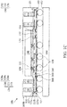
- FIG. 1A is a cross-sectional view of a semiconductor package assembly 10a in accordance with some embodiments of the disclosure.
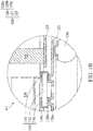
- FIG. 1B is an enlarged view of an area A1 in FIG. 1A , showing a multi-layer ceramic capacitor (MLCC) 150 embedded in an RDL structure.
- the semiconductor package assembly 10a is a wafer-level semiconductor package assembly, for example, a flip-chip semiconductor package assembly.
- the semiconductor package assembly 10a includes at least one wafer-level semiconductor package 100a mounted on a base 600.
- the wafer-level semiconductor package 100a includes a system-on-chip (SOC) package.
- the base 600 includes a printed circuit board (PCB) and may be formed of polypropylene (PP).
- the base 600 may include a package substrate.
- the base 600 may be a single layer or a multilayer structure.
- a plurality of conductive pads (not shown) and conductive traces (not shown) electrically coupled thereto are disposed on a surface 602 of the base 600 and/or in the base 600.
- the conductive traces may include signal trace segments and power/ground trace segments, which are used for the input/output (I/O) connections of the semiconductor package 100a.
- the semiconductor package 100a is mounted directly on the conductive traces.
- the conductive pads disposed on the surface 602 are connected to different terminals of the conductive traces. In this case, these conductive pads are used for the semiconductor package 100a mounted directly thereon.
- the semiconductor package 100a is mounted on the surface 602 of the base 600 by a bonding process.
- the semiconductor package 100a includes a plurality of conductive structures 130 that is mounted on and electrically coupled to the base 600 by the bonding process.
- the semiconductor package 100a includes a semiconductor die 100 (such as a SOC die) and an RDL structure 126.
- the SOC die may include a logic die including a central processing unit (CPU), a graphics processing unit (GPU), a dynamic random access memory (DRAM) controller or any combination thereof.
- the conductive structures 130 may comprise a conductive bump structure such as a copper bump or a solder bump structure, a conductive pillar structure, a conductive wire structure, or a conductive paste structure.
- the semiconductor die 100 is fabricated by flip-chip technology.
- Pads 109 of the semiconductor die 100 are electrically connected to the circuitry (not shown) of the semiconductor die 100.
- the pads 109 belong to the uppermost metal layer of the interconnection structure (not shown) of the semiconductor die 100.
- the pads 109 of the semiconductor die 100 are in contact with the corresponding conductive structures 111, for example, conductive bumps, posts or solder pastes. It should be noted that the number of semiconductor dies 100 integrated in the semiconductor package assembly 10a is not limited to that disclosed in the embodiment.
- the RDL structure 126 which is also referred to as a fan-out structure, has a first surface 101 and a second surface 103 opposite thereto.
- the semiconductor die 100a is disposed on the first surface 101 of the RDL structure 126.
- the semiconductor die 100 of the semiconductor package 100a is connected to the RDL structure 126 through conductive structures 111.
- the RDL structure 126 includes one or more conductive traces disposed in an inter-metal dielectric (IMD) layer 120.
- IMD inter-metal dielectric
- a plurality of first conductive traces 123 is disposed at a first layer-level of the IMD layer 120 and at least one of the plurality of first conductive traces 123 is electrically coupled to the semiconductor die 100.
- a plurality of second conductive traces 121 is disposed at a second layer-level different from the first layer-level of the IMD layer 120.
- the IMD layer 120 may include first, second, third sub-dielectric layers 120a, 120b, and 120c successively stacked from the second surface 103 of the RDL structure 126 toward the first surface 101 of the RDL structure 126, such that the first conductive traces 123 are positioned on the third sub-dielectric layer 120c and the second conductive traces 121 are positioned on the second sub-dielectric layer 120b and covered by the first sub-dielectric layer 120a. Also, the first conductive traces 123 are separated from the second conductive trace 121 by the second sub-dielectric layer 120b.
- the IMD layer 120 may be formed of organic materials, which include a polymer base material, non-organic materials, which include silicon nitride (SiNx), silicon oxide (SiOx), graphene, or the like.
- the first, second, third sub-dielectric layers 120a, 120b, and 120c are made of a polymer base material, in which the first sub-dielectric layer 120a has a thickness of about 12 ⁇ m and the second sub-dielectric layer 120b has a thickness of about 24 ⁇ m.
- the IMD layer 120 is a high-k dielectric layer (k is the dielectric constant of the dielectric layer). In some other embodiments, the IMD layer 120 may be formed of a photo sensitive material, which includes a dry film photoresist, or a taping film.
- Pad portions of the second conductive traces 121 are exposed to openings of the first sub-dielectric layers 120a and connected to the conductive structures 130 that are disposed on the second surface 103 of the RDL structure 126. Also, it should be noted that the number of conductive traces and the number of sub-dielectric layers of the RDL structure 126 shown in FIG. 1A is only an example and is not a limitation to the present invention.
- the semiconductor package 100a further includes at least one electronic component that is an integrated passive device (IPD) embedded in the RDL structure 126.
- the IPD is electrically coupled to the semiconductor die 100 through the RDL structure 126.
- the IPD is a multi-layer ceramic capacitor (MLCC) or a chip-cap capacitor.
- the IPD may include a capacitor, an inductor, a resistor, or a combination thereof.
- the IPD includes at least one electrode electrically coupled to one of the plurality of second conductive traces 121.
- the IPD is a multi-layer ceramic capacitor (MLCC) 150, as shown in FIGS. 1A and 1B .
- the MLCC 150 is electrically coupled to the semiconductor die 100.
- the MLCC 150 includes a body 152 and first and second electrode layers 154 and 156 respectively disposed on two ends of the body 152. Moreover, sidewalls, portions of an upper surface, and a lower surface of the body 152 are covered by the first and second electrode layers 154 and 156.
- the first and second electrode layers 154 and 156 are respectively electrically coupled to at least two of the second conductive traces 121.
- the semiconductor package 100a further includes a molding compound 104 disposed on the first surface 101 of the RDL structure 126 and covering and surrounding the semiconductor die 100.
- the molding compound 104 may be formed of an epoxy, a resin, a moldable polymer, or the like. The molding compound 104 may be applied while substantially liquid, and then may be cured through a chemical reaction, such as in an epoxy or resin.
- the molding compound 104 may be an ultraviolet (UV) or thermally cured polymer applied as a gel or malleable solid capable of being disposed around the semiconductor die 100, and then may be cured through a UV or thermal curing process. The molding compound 104 may be cured with a mold (not shown).
- the molding compound 104 includes vias 106 passing through therein.
- the vias 106 are electrically coupled to the second conductive traces 121 of the RDL structure 126.
- the semiconductor die 100 may be surrounded by the vias 106.
- the vias 106 may comprise through package vias (TPVs) formed of copper.
- the conductive structures 130 are separated from the molding compound 104 through the RDL structure 126. In other words, the conductive structures 130 are free from contact with the molding compound 104.
- the conductive structures 130 may comprise a conductive bump structure (such as a copper or solder bump structure), a conductive pillar structure, a conductive wire structure, or a conductive paste structure.
- the semiconductor package assembly 10a is designed to fabricate the MLCC 150 embedded in the RDL structure 126.
- the MLCC 150 provides a comparable process capability in the semiconductor package assembly.
- the semiconductor package assembly 10a may help to improve the surface-mount technology (SMT) yield even when the semiconductor die (e.g., the semiconductor die 100) is replaced.
- the signal integrity/power integrity (SI/PI) performance of the embedded MLCC 150 can be improved due to the shortened routing path between the semiconductor die (e.g., the semiconductor die 100) and the MLCC 150.
- the embedded MLCC 150 can provide design flexibility for the system integration of the semiconductor package assembly 10a.
- FIG. 1C is a cross-sectional view of an exemplary semiconductor package assembly 10b in accordance with some embodiments of the disclosure. Descriptions of elements of the embodiments hereinafter that are the same as or similar to those previously described with reference to FIG. 1A are omitted for brevity.
- the semiconductor package assembly 10b is similar to the semiconductor package assembly 10a shown in FIG. 1A , except a semiconductor package 100b of the semiconductor package assembly 10b further includes a semiconductor die 160, such as an SOC die, embedded in the RDL structure 126.
- the semiconductor die 160 is electrically coupled to the semiconductor die 100 through the RDL structure 126.
- the semiconductor die 160 includes at least one pad electrically coupled to one of the plurality of second conductive traces 121.
- the semiconductor die 160 includes pads 164 that are electrically coupled to the second conductive traces 121.
- the semiconductor package assembly 10b is designed to fabricate the MLCC 150 and a semiconductor die 160 embedded in the RDL structure 126.
- the MLCC 150 and the semiconductor die 160 provide a comparable process capability in the semiconductor package assembly.
- the semiconductor package assembly 10b may help to improve the SMT yield even when the semiconductor die (e.g., the semiconductor die 100) is replaced.
- the SI/PI performance of the embedded MLCC 150 and semiconductor die 160 can be improved due to the shortened routing path between the semiconductor die (e.g., the semiconductor die 100) and the MLCC 150 and semiconductor die 160.
- the embedded MLCC 150 and semiconductor die 160 can provide design flexibility for the system integration of the semiconductor package assembly 10b.
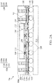
- FIG. 2A is a cross-sectional view of an exemplary semiconductor package assembly 10c in accordance with some embodiments of the disclosure.
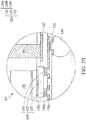
- FIG. 2B is an enlarged view of an area A2 in FIG. 2A , showing a chip-cap capacitor 150' embedded in an RDL structure. Descriptions of elements of the embodiments hereinafter that are the same as or similar to those previously described with reference to FIGS. 1A and 1B are omitted for brevity.
- the semiconductor package assembly 10c is similar to the semiconductor package assembly 10a shown in FIG. 1A , except the semiconductor package 100c of the semiconductor package assembly 10c includes a chip-cap capacitor 150', that replaces the MLCC 150 shown in FIGS. 1A and 1B to be embedded in the RDL structure 126.
- the chip-cap capacitor 150' is electrically coupled to the semiconductor die 100.
- the chip-cap capacitor 150' includes a body 152' and first and second electrode layers 154' and 156' respectively disposed on two ends of the body 152'.
- the first and second electrode layers 154' and 156' expose sidewalls, portions of a lower surface of the body 152'.
- the first and second electrode layers 154' and 156' are respectively electrically coupled to at least two of the second conductive traces 121.
- the semiconductor package assembly 10c is designed to fabricate the chip-cap capacitor 150' embedded in the RDL structure 126.
- the chip-cap capacitor 150' provides a comparable process capability in the semiconductor package assembly.
- the semiconductor package assembly 10c may help to improve the SMT yield even when the semiconductor die (e.g., the semiconductor die 100) is replaced.
- the SI/PI performance of the embedded chip-cap capacitor 150' can be improved due to the shortened routing path between the semiconductor die (e.g., the semiconductor die 100) and the chip-cap capacitor 150'.
- the embedded chip-cap capacitor 150' can provide design flexibility for the system integration of the semiconductor package assembly 10c.
- FIG. 2C is a cross-sectional view of an exemplary semiconductor package assembly 10d in accordance with some embodiments of the disclosure. Descriptions of elements of the embodiments hereinafter that are the same as or similar to those previously described with reference to FIG. 1C are omitted for brevity.
- the semiconductor package assembly 10d is similar to the semiconductor package assembly 10c shown in FIG. 2A , except a semiconductor package 100d of the semiconductor package assembly 10d further includes a semiconductor die 160, such as an SOC die, embedded in the RDL structure 126.
- the semiconductor die 160 is electrically coupled to the semiconductor die 100 through the RDL structure 126.
- the semiconductor die 160 includes pads 164 that are electrically coupled to the second conductive traces 121.
- the semiconductor package assembly 10d is designed to fabricate the chip-cap capacitor 150' and a semiconductor die 160 embedded in the RDL structure 126.
- the chip-cap capacitor 150' and the semiconductor die 160 provides a comparable process capability in the semiconductor package assembly.
- the semiconductor package assembly 10d may help to improve the SMT yield even when the semiconductor die (e.g., the semiconductor die 100) is replaced.
- the SI/PI performance of the embedded chip-cap capacitor 150' and semiconductor die 160 can be improved due to the shortened routing path between the semiconductor die (e.g., the semiconductor die 100) and the chip-cap capacitor 150' and semiconductor die 160.
- the embedded chip-cap capacitor 150' and semiconductor die 160 can provide design flexibility for the system integration of the semiconductor package assembly 10d.
- FIG. 3 is a cross-sectional view of a semiconductor package assembly including a package on package (PoP) structure in accordance with some embodiments of the disclosure. Descriptions of elements of the embodiments hereinafter that are the same as or similar to those previously described with reference to FIGS. 1A-1C or 2A-2C are omitted for brevity.
- the semiconductor package 100e is similar to the semiconductor package 100c shown in FIG. 2A , except the semiconductor package 100e further includes a RDL structure 226 disposed on the semiconductor die 100 and the molding compound 104, such that the RDL structure 226 is separated from the RDL structure 126 by the semiconductor die 100 and the molding compound 104. Moreover, the vias 106 passing through the molding compound 104 form an electrical connection between the RDL structures 126 and 226.
- the RDL structure 226 has a first surface 201 and a second surface 203 opposite thereto.
- the first surface 201 of the RDL structure 226 is disposed on the semiconductor die 100 and the molding compound 104. Namely, compared to the second surface 203, the first surface 201 is close to the semiconductor die 100 and is in contact with the molding compound 104.
- the RDL structure 226 may one or more conductive traces disposed in an IMD layer 220.
- a plurality of conductive traces 221 and a plurality of vias 223 are disposed in the IMD layer 220 and at least one of the plurality of conductive traces 221 is electrically coupled to the via 106.
- the IMD layer 220 is similar to the IMD layer 120 and may include first, second, third sub-dielectric layers 220a, 220b, and 220c successively stacked from the second surface 203 of the RDL structure 226 toward the first surface 201 of the RDL structure 2262. Also, the IMD layer 220 may be formed of a material the same as or similar to that of the IMD layer 120.
- the RDL structure 226 is coupled to the RDL structure 126 by vias 106 passing through the molding compound 104 between the RDL structure 126 and the RDL structure 226.
- the chip-cap capacitor 150' embedded in the RDL structure 126 may be replaced by the MLCC 150, as shown in FIG. 1A .
- a semiconductor die 160 and the chip-cap capacitor 150' or the MLCC 150 may be embedded in the RDL structure 126 together, as shown in FIG. 1C or 2C .
- the semiconductor package assembly 10e includes a semiconductor package 200a stacked on the semiconductor package 100e (e.g., an SOC package) by a bonding process.
- the semiconductor package 200a may include a memory package, for example, a dynamic random access memory (DRAM) package.
- the semiconductor package 200a includes a plurality of conductive structures 328 mounted on the semiconductor package 100e.
- the Semiconductor package 200a is coupled to the RDL structure 126 by the RDL structure 226 and the vias 106 of the semiconductor package 100e.
- the semiconductor package 200a comprises a RDL structure 326, at least one semiconductor die (e.g., two DRAM dies 300 and 302) and a molding compound 304.
- the RDL structure 326 has opposite surfaces 301 and 303.
- the surface 301 is provided for semiconductor dies mounted thereon, and the surface 303 is provided for conductive structures 328 (such as bumps) attached thereon.
- the RDL structure 326 may one or more conductive traces disposed in an IMD layer 320.
- a plurality of first conductive traces 321 and a plurality of second conductive traces 323 are disposed at different layer-levels of the IMD layer 320.
- the structure and material of the IMD layer 320 are similar to that of the IMD layer 120.
- the IMD layer 320 may include first, second, third sub-dielectric layers 320a, 320b, and 320c successively stacked from the surface 303 of the RDL structure 326 toward the surface 301 of the RDL structure 326.
- Pad portions of the first conductive traces 321 are exposed to openings of the first sub-dielectric layer 320a. It should be noted that the number of conductive traces and the number sub-dielectric layers of the IMD layer 320 shown in FIG. 3 is only an example and is not a limitation of the present invention
- the semiconductor dies 302 and 300 are successively stacked on the surface 301 of the RDL structure 326, in which the semiconductor die 302 is mounted on the RDL structure 326 with a paste (not shown). Also, the semiconductor die 300 is stacked on the semiconductor die 302 with a paste (not shown). The semiconductor die 302 has pads 308 thereon, and the semiconductor die 300 has pads 310 thereon.
- the pads 308 and 310 may be coupled to pads 325 of the RDL structure 326 by bonding wires, such as bonding wires 314 and 316, respectively. It should be noted that the number of stacked semiconductor dies in the semiconductor package 200a is not limited to the disclosed embodiment. Alternatively, the two semiconductor dies 300 and 302 may be arranged side by side.
- the molding compound 304 is disposed on the surface 301 of the RDL structure 326. Moreover, the molding compound 304 covers and surrounds the two semiconductor dies 300 and 302.
- the molding compound 304 may be formed of a material the same as or similar to that of the molding compound 104.
- conductive structures 328 are disposed on the surface 303 of the RDL structure 326 and electrically coupled between the first conductive trace 321 of the RDL structure 326 and the vias 223 of the RDL structure 226.
- the semiconductor package 200a is electrically coupled to the RDL structure 126 of the semiconductor package 100e.
- conductive structures 328 may include a copper or solder bump structure, a conductive pillar structure, a conductive wire structure, or a conductive paste structure.
- FIG. 4 is a cross-sectional view of a semiconductor package assembly 10f including a semiconductor package 100f with two semiconductor dies 400a and 400b arranged side-by-side in accordance with some other embodiments of the disclosure. Descriptions of elements of the embodiments hereinafter that are the same as or similar to those previously described with reference to FIGS. 1A-1B or 2A-2B are omitted for brevity.
- the semiconductor package 100f may be an SOC package of the semiconductor package assembly 100f and include two semiconductor dies 400a and 400b arranged side-by-side.
- at least one of the semiconductor dies 400a and 400b is a SOC die.
- the semiconductor dies 400a and 400b are SOC die.
- the semiconductor die 400a is a SOC die
- the semiconductor dies 400b is a memory die, such as a DRAM die.
- the chip-cap capacitor 150' is embedded in the RDL structure 126 and coupled to the SOC die (e.g., the semiconductor die 400a). Therefore, the semiconductor package 100f of the semiconductor package assembly 10f includes a pure SOC package or a hybrid SOC package. However, the number and the arrangement of semiconductor dies are not limited to the disclosed embodiment.
- the chip-cap capacitor 150' embedded in the RDL structure 126 may be replaced by the MLCC 150, as shown in FIG. 1A .
- a semiconductor die 160 and the chip-cap capacitor 150' or the MLCC 150 may be embedded in the RDL structure 126 together, as shown in FIG. 1C or 2C .
- Embodiments shown in FIGS. 3 and 4 provide a semiconductor package assembly.
- the semiconductor package assembly is designed to fabricate an IPD being an MLCC or chip-cap capacitor embedded in an RDL structure.
- the semiconductor package assembly may help to improve the SMT yield even when the semiconductor die (the SOC die) is replaced. Additionally, the SI/PI performance of the embedded IPD can be improved due to the shortened routing path between the semiconductor die (the SOC die) and the IPD.
- the embedded IPD can provide the design flexibility for the system integration of the semiconductor package assembly.
Landscapes
- Semiconductor Integrated Circuits (AREA)
- Production Of Multi-Layered Print Wiring Board (AREA)
- Engineering & Computer Science (AREA)
- Manufacturing & Machinery (AREA)
Claims (11)
- Ensemble de boîtiers de semi-conducteur (10a, 10b), comprenant :un premier boîtier de semi-conducteur (100a, 100b), comprenant :une première structure de couche de redistribution, RDL, (126) présentant une première surface (101) et une deuxième surface (103) opposée à celle-ci ;une première puce de semi-conducteur (100) disposée sur la première surface (101) de la première structure de couche RDL (126) ;un premier composé de moulage (104) disposé sur la première surface (101) de la première structure de couche RDL (126) et entourant la première puce de semi-conducteur (100) ; etun composant électronique intégré dans la première structure de couche RDL (126) et couplé électriquement à la première puce de semi-conducteur (100) par l'intermédiaire de la première structure de couche RDL (126) ;dans lequel la première structure de couche RDL (126) comprend :une première couche diélectrique intermétallique, IMD, (120) ;une pluralité de premières traces conductrices (123), à un premier niveau de couche de la première couche diélectrique IMD (120), et dans lequel une trace de la pluralité de premières traces conductrices (123) est couplée électriquement à la première puce de semi-conducteur (100) ; etune pluralité de secondes traces conductrices (121), à un second niveau de couche différent du premier niveau de couche de la première couche diélectrique IMD (120) ; etcaractérisé en ce que le composant électronique est un condensateur céramique multicouche (150), comprenant :un corps (152) ; etdes première et seconde couches d'électrode (154, 156) respectivement disposées sur des extrémités respectives du corps (152), de sorte que des parois latérales, des parties d'une surface supérieure et une surface inférieure du corps (152) sont recouvertes par les première et seconde couches d'électrode (154, 156), dans lequel les première et seconde couches d'électrode (154, 156) sont couplées électriquement à au moins une trace respective de la pluralité de secondes traces conductrices (121).
- Ensemble de boîtiers de semi-conducteur (10c, 10d, 10e, 10f), comprenant :un premier boîtier de semi-conducteur (100c, 100d, 100e, 100f), comprenant :une première structure de couche de redistribution, RDL, (126), présentant une première surface (101) et une deuxième surface (103) opposée à celle-ci ;une première puce de semi-conducteur (100) disposée sur la première surface (101) de la première structure de couche RDL (126) ;un premier composé de moulage (104) disposé sur la première surface (101) de la première structure de couche RDL (126) et entourant la première puce de semi-conducteur (100) ; etun composant électronique intégré dans la première structure de couche RDL (126) et couplé électriquement à la première puce de semi-conducteur (100) par l'intermédiaire de la première structure de couche RDL (126) ;dans lequel la première structure de couche RDL (126) comprend :une première couche diélectrique intermétallique, IMD, (120) ;une pluralité de premières traces conductrices (123), à un premier niveau de couche de la première couche diélectrique IMD (120), et dans lequel une trace de la pluralité de premières traces conductrices (123) est couplée électriquement à la première puce de semi-conducteur (100) ; etune pluralité de secondes traces conductrices (121), à un second niveau de couche différent du premier niveau de couche de la première couche diélectrique IMD (120) ; etcaractérisé en ce que le composant électronique est un condensateur pavé (150'), comprenant :un corps (152') ; etdes première et seconde couches d'électrode (154', 156') disposées sur des extrémités respectives du corps (152') et exposant des parois latérales, et des parties d'une surface inférieure du corps (152'), dans lequel les première et seconde couches d'électrode (154', 156') sont couplées électriquement à au moins une trace respective de la pluralité de secondes traces conductrices (121).
- Ensemble de boîtiers de semi-conducteur (10b, 10d) selon la revendication 1 ou 2, dans lequel le premier boîtier de semi-conducteur (100b, 100d) comprend en outre une deuxième puce de semi-conducteur (160) intégrée dans la première structure de couche RDL (126).
- Ensemble de boîtiers de semi-conducteur (10a, 10b, 10c, 10d, 10e, 10f) selon l'une quelconque des revendications précédentes, dans lequel le premier boîtier de semi-conducteur (100a, 100b, 100c, 100d, 100e, 100f) comprend en outre une pluralité de premières structures conductrices (130) disposées sur la deuxième surface (103) de la première structure de couche RDL (126) et couplées électriquement à la première structure de couche RDL (126).
- Ensemble de boîtiers de semi-conducteur (10a, 10b, 10c, 10d, 10e, 10f) selon la revendication 4, comprenant en outre une carte de circuit imprimé (600) couplée électriquement à la pluralité de premières structures conductrices (130).
- Ensemble de boîtiers de semi-conducteur (10e) selon l'une quelconque des revendications précédentes, dans lequel le premier boîtier de semi-conducteur (100e) comprend :une deuxième structure de couche RDL (226) disposée sur la première puce de semi-conducteur (100) et le premier composé de moulage (104), de sorte que la deuxième structure de couche RDL (226) est séparée de la première structure de couche RDL (126) par la première puce de semi-conducteur (100) et le premier composé de moulage (104) ; etune pluralité de premiers trous d'interconnexion (106) traversant le premier composé de moulage (104) en vue de former une connexion électrique entre les première et deuxième structures de couche RDL (126, 226).
- Ensemble de boîtiers de semi-conducteur (10e) selon la revendication 6, comprenant en outre :
un second boîtier de semi-conducteur (200a) empilé sur le premier boîtier de semi-conducteur (100a), comprenant :une troisième structure de couche RDL (326) couplée électriquement à la deuxième structure de couche RDL (226) et présentant une troisième surface (301) et une quatrième surface (303) opposée à celle-ci ;une troisième puce de semi-conducteur (300) disposée sur la troisième surface (301) de la troisième structure de couche RDL (326) ; etun second composé de moulage (304) disposé sur la troisième surface (301) de la troisième structure de couche RDL (326) et entourant la troisième puce de semi-conducteur (300). - Ensemble de boîtiers de semi-conducteur (10e) selon la revendication 7, dans lequel le second boîtier de semi-conducteur (200a) comprend en outre une pluralité de secondes structures conductrices (328) disposées sur la quatrième surface (303) de la troisième structure de couche RDL (326) et couplées électriquement à la deuxième structure de couche RDL (226).
- Ensemble de boîtiers de semi-conducteur (10e) selon la revendication 7 ou 8, dans lequel le premier boîtier de semi-conducteur (100e) est un boîtier de « système sur puce » (SoC), et le second boîtier de semi-conducteur (200a) est un boîtier de mémoire vive dynamique (DRAM).
- Ensemble de boîtiers de semi-conducteur (10f) selon l'une quelconque des revendications 1 à 5, dans lequel le premier boîtier de semi-conducteur (100f) comprend en outre une quatrième puce de semi-conducteur (400b) disposée sur la première surface (101) de la première structure de couche RDL (126), de sorte que les première et quatrième puces de semi-conducteur (400a, 400b) sont agencées en côte à côte.
- Ensemble de boîtiers de semi-conducteur (10f) selon la revendication 10, dans lequel la première puce de semi-conducteur (400a) est une puce de système SoC, et la quatrième puce de semi-conducteur (400b) est une puce de mémoire DRAM.
Applications Claiming Priority (3)
| Application Number | Priority Date | Filing Date | Title |
|---|---|---|---|
| US201562139932P | 2015-03-30 | 2015-03-30 | |
| US201562157046P | 2015-05-05 | 2015-05-05 | |
| US15/047,980 US10217724B2 (en) | 2015-03-30 | 2016-02-19 | Semiconductor package assembly with embedded IPD |
Publications (3)
| Publication Number | Publication Date |
|---|---|
| EP3076429A2 EP3076429A2 (fr) | 2016-10-05 |
| EP3076429A3 EP3076429A3 (fr) | 2016-12-07 |
| EP3076429B1 true EP3076429B1 (fr) | 2020-05-06 |
Family
ID=55527457
Family Applications (1)
| Application Number | Title | Priority Date | Filing Date |
|---|---|---|---|
| EP16160070.5A Active EP3076429B1 (fr) | 2015-03-30 | 2016-03-14 | Ensemble de boîtier de semi-conducteur avec une capacité de type mlcc ou chip-cap incorporé |
Country Status (4)
| Country | Link |
|---|---|
| US (1) | US10217724B2 (fr) |
| EP (1) | EP3076429B1 (fr) |
| CN (1) | CN106024754B (fr) |
| TW (1) | TWI642152B (fr) |
Families Citing this family (24)
| Publication number | Priority date | Publication date | Assignee | Title |
|---|---|---|---|---|
| US10283443B2 (en) * | 2009-11-10 | 2019-05-07 | Taiwan Semiconductor Manufacturing Co., Ltd. | Chip package having integrated capacitor |
| US20170040266A1 (en) | 2015-05-05 | 2017-02-09 | Mediatek Inc. | Fan-out package structure including antenna |
| US9768145B2 (en) | 2015-08-31 | 2017-09-19 | Taiwan Semiconductor Manufacturing Company, Ltd. | Methods of forming multi-die package structures including redistribution layers |
| TWI649856B (zh) * | 2016-05-13 | 2019-02-01 | Xintec Inc. | 晶片封裝體與其製造方法 |
| CN106558574A (zh) * | 2016-11-18 | 2017-04-05 | 华为技术有限公司 | 芯片封装结构和方法 |
| KR101982049B1 (ko) | 2016-11-23 | 2019-05-24 | 삼성전기주식회사 | 팬-아웃 반도체 패키지 |
| TWI618218B (zh) * | 2017-01-26 | 2018-03-11 | Advanced Semiconductor Engineering, Inc. | 半導體封裝結構 |
| TWI655739B (zh) * | 2018-04-19 | 2019-04-01 | 南亞電路板股份有限公司 | 封裝結構及其形成方法 |
| US10593628B2 (en) * | 2018-04-24 | 2020-03-17 | Advanced Micro Devices, Inc. | Molded die last chip combination |
| DE102018212273A1 (de) * | 2018-07-24 | 2020-01-30 | Robert Bosch Gmbh | Elektronikeinheit |
| TWI659515B (zh) | 2018-07-26 | 2019-05-11 | 欣興電子股份有限公司 | 封裝結構及其製造方法 |
| US10672712B2 (en) | 2018-07-30 | 2020-06-02 | Advanced Micro Devices, Inc. | Multi-RDL structure packages and methods of fabricating the same |
| CN110854107B (zh) * | 2018-08-20 | 2025-07-25 | 盛合晶微半导体(江阴)有限公司 | 扇出型天线封装结构及封装方法 |
| FR3096808B1 (fr) * | 2019-05-29 | 2021-10-22 | Saint Gobain Pont A Mousson | Dispositif d’identification, élément tubulaire et procédé correspondants |
| US11367628B2 (en) * | 2019-07-16 | 2022-06-21 | Advanced Micro Devices, Inc. | Molded chip package with anchor structures |
| TWI734545B (zh) * | 2020-07-03 | 2021-07-21 | 財團法人工業技術研究院 | 半導體封裝結構 |
| KR102774741B1 (ko) * | 2020-07-31 | 2025-03-04 | 에스케이하이닉스 주식회사 | 적층 반도체 칩을 포함하는 반도체 패키지 |
| US12476194B2 (en) * | 2021-01-06 | 2025-11-18 | Mediatek Singapore Pte. Ltd. | Semiconductor structure |
| US12170252B2 (en) * | 2021-09-29 | 2024-12-17 | International Business Machines Corporation | Electronic substrate stacking |
| US12506134B2 (en) * | 2022-10-27 | 2025-12-23 | Micron Technology, Inc. | Fan-out packaging for a multichip package |
| US20240178154A1 (en) * | 2022-11-29 | 2024-05-30 | Texas Instruments Incorporated | Electronic device package emi shielding with grounded mold interconnect |
| US20240282715A1 (en) * | 2023-02-17 | 2024-08-22 | Advanced Semiconductor Engineering, Inc. | Semiconductor device package and method of manufacturing the same |
| US20240413029A1 (en) * | 2023-06-12 | 2024-12-12 | Microsoft Technology Licensing, Llc | Embedding an electronic component in a core of an integrated circuit substrate |
| US20250118648A1 (en) * | 2023-10-05 | 2025-04-10 | Qorvo Us, Inc. | Multilevel system-in-package module with embedded die and redistribution bottom features |
Family Cites Families (25)
| Publication number | Priority date | Publication date | Assignee | Title |
|---|---|---|---|---|
| TWI234253B (en) | 2002-05-31 | 2005-06-11 | Fujitsu Ltd | Semiconductor device and manufacturing method thereof |
| JP4552524B2 (ja) | 2004-06-10 | 2010-09-29 | パナソニック株式会社 | 複合型電子部品 |
| JP4912716B2 (ja) | 2006-03-29 | 2012-04-11 | 新光電気工業株式会社 | 配線基板の製造方法、及び半導体装置の製造方法 |
| US7242081B1 (en) | 2006-04-24 | 2007-07-10 | Advanced Semiconductor Engineering Inc. | Stacked package structure |
| KR100796523B1 (ko) | 2006-08-17 | 2008-01-21 | 삼성전기주식회사 | 전자부품 내장형 다층 인쇄배선기판 및 그 제조방법 |
| US8133762B2 (en) | 2009-03-17 | 2012-03-13 | Stats Chippac, Ltd. | Semiconductor device and method of providing z-interconnect conductive pillars with inner polymer core |
| US7476563B2 (en) | 2006-11-17 | 2009-01-13 | Freescale Semiconductor, Inc. | Method of packaging a device using a dielectric layer |
| US7651889B2 (en) | 2007-09-13 | 2010-01-26 | Freescale Semiconductor, Inc. | Electromagnetic shield formation for integrated circuit die package |
| US8130507B2 (en) * | 2008-03-24 | 2012-03-06 | Ngk Spark Plug Co., Ltd. | Component built-in wiring board |
| US7858441B2 (en) | 2008-12-08 | 2010-12-28 | Stats Chippac, Ltd. | Semiconductor package with semiconductor core structure and method of forming same |
| US8941222B2 (en) | 2010-11-11 | 2015-01-27 | Advanced Semiconductor Engineering Inc. | Wafer level semiconductor package and manufacturing methods thereof |
| TWI452665B (zh) | 2010-11-26 | 2014-09-11 | 矽品精密工業股份有限公司 | 具防靜電破壞及防電磁波干擾之封裝件及其製法 |
| KR101434003B1 (ko) | 2011-07-07 | 2014-08-27 | 삼성전기주식회사 | 반도체 패키지 및 그 제조 방법 |
| US8786060B2 (en) | 2012-05-04 | 2014-07-22 | Advanced Semiconductor Engineering, Inc. | Semiconductor package integrated with conformal shield and antenna |
| US8878360B2 (en) | 2012-07-13 | 2014-11-04 | Intel Mobile Communications GmbH | Stacked fan-out semiconductor chip |
| US9153542B2 (en) | 2012-08-01 | 2015-10-06 | Advanced Semiconductor Engineering, Inc. | Semiconductor package having an antenna and manufacturing method thereof |
| KR20150025129A (ko) | 2013-08-28 | 2015-03-10 | 삼성전기주식회사 | 전자 소자 모듈 및 그 제조 방법 |
| KR102157551B1 (ko) | 2013-11-08 | 2020-09-18 | 삼성전자주식회사 | 반도체 패키지 및 그 제조 방법 |
| US20150262902A1 (en) * | 2014-03-12 | 2015-09-17 | Invensas Corporation | Integrated circuits protected by substrates with cavities, and methods of manufacture |
| US9570418B2 (en) * | 2014-06-06 | 2017-02-14 | Taiwan Semiconductor Manufacturing Company, Ltd. | Structure and method for package warpage control using dummy interconnects |
| WO2016092692A1 (fr) | 2014-12-12 | 2016-06-16 | 株式会社メイコー | Module de circuit moulé et procédé de fabrication dudit module |
| US9633974B2 (en) * | 2015-03-04 | 2017-04-25 | Apple Inc. | System in package fan out stacking architecture and process flow |
| US9978729B2 (en) * | 2015-03-06 | 2018-05-22 | Mediatek Inc. | Semiconductor package assembly |
| US20170040266A1 (en) | 2015-05-05 | 2017-02-09 | Mediatek Inc. | Fan-out package structure including antenna |
| US20160329299A1 (en) | 2015-05-05 | 2016-11-10 | Mediatek Inc. | Fan-out package structure including antenna |
-
2016
- 2016-02-19 US US15/047,980 patent/US10217724B2/en active Active
- 2016-03-14 EP EP16160070.5A patent/EP3076429B1/fr active Active
- 2016-03-28 CN CN201610182901.6A patent/CN106024754B/zh active Active
- 2016-03-29 TW TW105109810A patent/TWI642152B/zh not_active IP Right Cessation
Non-Patent Citations (1)
| Title |
|---|
| None * |
Also Published As
| Publication number | Publication date |
|---|---|
| US20160293581A1 (en) | 2016-10-06 |
| TW201707164A (zh) | 2017-02-16 |
| EP3076429A2 (fr) | 2016-10-05 |
| US10217724B2 (en) | 2019-02-26 |
| CN106024754B (zh) | 2019-05-03 |
| TWI642152B (zh) | 2018-11-21 |
| EP3076429A3 (fr) | 2016-12-07 |
| CN106024754A (zh) | 2016-10-12 |
Similar Documents
| Publication | Publication Date | Title |
|---|---|---|
| EP3076429B1 (fr) | Ensemble de boîtier de semi-conducteur avec une capacité de type mlcc ou chip-cap incorporé | |
| US11728292B2 (en) | Semiconductor package assembly having a conductive electromagnetic shield layer | |
| US10177125B2 (en) | Semiconductor package assembly | |
| US20190252351A1 (en) | Semiconductor package structure having an antenna pattern electrically coupled to a first redistribution layer (rdl) | |
| US9978729B2 (en) | Semiconductor package assembly | |
| US10692789B2 (en) | Stacked fan-out package structure | |
| TWI582858B (zh) | 半導體封裝組件及其製造方法 | |
| EP3273475B1 (fr) | Structure de boîtier de sortance | |
| US9997498B2 (en) | Semiconductor package assembly | |
| US10147674B2 (en) | Semiconductor package assembly |
Legal Events
| Date | Code | Title | Description |
|---|---|---|---|
| PUAI | Public reference made under article 153(3) epc to a published international application that has entered the european phase |
Free format text: ORIGINAL CODE: 0009012 |
|
| AK | Designated contracting states |
Kind code of ref document: A2 Designated state(s): AL AT BE BG CH CY CZ DE DK EE ES FI FR GB GR HR HU IE IS IT LI LT LU LV MC MK MT NL NO PL PT RO RS SE SI SK SM TR |
|
| AX | Request for extension of the european patent |
Extension state: BA ME |
|
| PUAL | Search report despatched |
Free format text: ORIGINAL CODE: 0009013 |
|
| AK | Designated contracting states |
Kind code of ref document: A3 Designated state(s): AL AT BE BG CH CY CZ DE DK EE ES FI FR GB GR HR HU IE IS IT LI LT LU LV MC MK MT NL NO PL PT RO RS SE SI SK SM TR |
|
| AX | Request for extension of the european patent |
Extension state: BA ME |
|
| RIC1 | Information provided on ipc code assigned before grant |
Ipc: H01L 25/16 20060101ALI20161103BHEP Ipc: H01L 25/10 20060101ALI20161103BHEP Ipc: H01L 23/538 20060101AFI20161103BHEP |
|
| STAA | Information on the status of an ep patent application or granted ep patent |
Free format text: STATUS: REQUEST FOR EXAMINATION WAS MADE |
|
| 17P | Request for examination filed |
Effective date: 20170517 |
|
| RBV | Designated contracting states (corrected) |
Designated state(s): AL AT BE BG CH CY CZ DE DK EE ES FI FR GB GR HR HU IE IS IT LI LT LU LV MC MK MT NL NO PL PT RO RS SE SI SK SM TR |
|
| STAA | Information on the status of an ep patent application or granted ep patent |
Free format text: STATUS: EXAMINATION IS IN PROGRESS |
|
| 17Q | First examination report despatched |
Effective date: 20190513 |
|
| GRAP | Despatch of communication of intention to grant a patent |
Free format text: ORIGINAL CODE: EPIDOSNIGR1 |
|
| STAA | Information on the status of an ep patent application or granted ep patent |
Free format text: STATUS: GRANT OF PATENT IS INTENDED |
|
| RIC1 | Information provided on ipc code assigned before grant |
Ipc: H01L 25/16 20060101ALI20191121BHEP Ipc: H01L 23/538 20060101AFI20191121BHEP Ipc: H01L 23/498 20060101ALN20191121BHEP Ipc: H01L 25/10 20060101ALI20191121BHEP |
|
| RIC1 | Information provided on ipc code assigned before grant |
Ipc: H01L 25/10 20060101ALI20191203BHEP Ipc: H01L 25/16 20060101ALI20191203BHEP Ipc: H01L 23/538 20060101AFI20191203BHEP Ipc: H01L 23/498 20060101ALN20191203BHEP |
|
| INTG | Intention to grant announced |
Effective date: 20191220 |
|
| GRAS | Grant fee paid |
Free format text: ORIGINAL CODE: EPIDOSNIGR3 |
|
| GRAA | (expected) grant |
Free format text: ORIGINAL CODE: 0009210 |
|
| STAA | Information on the status of an ep patent application or granted ep patent |
Free format text: STATUS: THE PATENT HAS BEEN GRANTED |
|
| AK | Designated contracting states |
Kind code of ref document: B1 Designated state(s): AL AT BE BG CH CY CZ DE DK EE ES FI FR GB GR HR HU IE IS IT LI LT LU LV MC MK MT NL NO PL PT RO RS SE SI SK SM TR |
|
| REG | Reference to a national code |
Ref country code: GB Ref legal event code: FG4D |
|
| REG | Reference to a national code |
Ref country code: CH Ref legal event code: EP Ref country code: AT Ref legal event code: REF Ref document number: 1268182 Country of ref document: AT Kind code of ref document: T Effective date: 20200515 |
|
| REG | Reference to a national code |
Ref country code: DE Ref legal event code: R096 Ref document number: 602016035486 Country of ref document: DE |
|
| REG | Reference to a national code |
Ref country code: IE Ref legal event code: FG4D |
|
| REG | Reference to a national code |
Ref country code: LT Ref legal event code: MG4D |
|
| REG | Reference to a national code |
Ref country code: NL Ref legal event code: MP Effective date: 20200506 |
|
| PG25 | Lapsed in a contracting state [announced via postgrant information from national office to epo] |
Ref country code: NO Free format text: LAPSE BECAUSE OF FAILURE TO SUBMIT A TRANSLATION OF THE DESCRIPTION OR TO PAY THE FEE WITHIN THE PRESCRIBED TIME-LIMIT Effective date: 20200806 Ref country code: FI Free format text: LAPSE BECAUSE OF FAILURE TO SUBMIT A TRANSLATION OF THE DESCRIPTION OR TO PAY THE FEE WITHIN THE PRESCRIBED TIME-LIMIT Effective date: 20200506 Ref country code: GR Free format text: LAPSE BECAUSE OF FAILURE TO SUBMIT A TRANSLATION OF THE DESCRIPTION OR TO PAY THE FEE WITHIN THE PRESCRIBED TIME-LIMIT Effective date: 20200807 Ref country code: PT Free format text: LAPSE BECAUSE OF FAILURE TO SUBMIT A TRANSLATION OF THE DESCRIPTION OR TO PAY THE FEE WITHIN THE PRESCRIBED TIME-LIMIT Effective date: 20200907 Ref country code: LT Free format text: LAPSE BECAUSE OF FAILURE TO SUBMIT A TRANSLATION OF THE DESCRIPTION OR TO PAY THE FEE WITHIN THE PRESCRIBED TIME-LIMIT Effective date: 20200506 Ref country code: IS Free format text: LAPSE BECAUSE OF FAILURE TO SUBMIT A TRANSLATION OF THE DESCRIPTION OR TO PAY THE FEE WITHIN THE PRESCRIBED TIME-LIMIT Effective date: 20200906 Ref country code: SE Free format text: LAPSE BECAUSE OF FAILURE TO SUBMIT A TRANSLATION OF THE DESCRIPTION OR TO PAY THE FEE WITHIN THE PRESCRIBED TIME-LIMIT Effective date: 20200506 |
|
| PG25 | Lapsed in a contracting state [announced via postgrant information from national office to epo] |
Ref country code: RS Free format text: LAPSE BECAUSE OF FAILURE TO SUBMIT A TRANSLATION OF THE DESCRIPTION OR TO PAY THE FEE WITHIN THE PRESCRIBED TIME-LIMIT Effective date: 20200506 Ref country code: HR Free format text: LAPSE BECAUSE OF FAILURE TO SUBMIT A TRANSLATION OF THE DESCRIPTION OR TO PAY THE FEE WITHIN THE PRESCRIBED TIME-LIMIT Effective date: 20200506 Ref country code: BG Free format text: LAPSE BECAUSE OF FAILURE TO SUBMIT A TRANSLATION OF THE DESCRIPTION OR TO PAY THE FEE WITHIN THE PRESCRIBED TIME-LIMIT Effective date: 20200806 Ref country code: LV Free format text: LAPSE BECAUSE OF FAILURE TO SUBMIT A TRANSLATION OF THE DESCRIPTION OR TO PAY THE FEE WITHIN THE PRESCRIBED TIME-LIMIT Effective date: 20200506 |
|
| REG | Reference to a national code |
Ref country code: AT Ref legal event code: MK05 Ref document number: 1268182 Country of ref document: AT Kind code of ref document: T Effective date: 20200506 |
|
| PG25 | Lapsed in a contracting state [announced via postgrant information from national office to epo] |
Ref country code: AL Free format text: LAPSE BECAUSE OF FAILURE TO SUBMIT A TRANSLATION OF THE DESCRIPTION OR TO PAY THE FEE WITHIN THE PRESCRIBED TIME-LIMIT Effective date: 20200506 Ref country code: NL Free format text: LAPSE BECAUSE OF FAILURE TO SUBMIT A TRANSLATION OF THE DESCRIPTION OR TO PAY THE FEE WITHIN THE PRESCRIBED TIME-LIMIT Effective date: 20200506 |
|
| PG25 | Lapsed in a contracting state [announced via postgrant information from national office to epo] |
Ref country code: ES Free format text: LAPSE BECAUSE OF FAILURE TO SUBMIT A TRANSLATION OF THE DESCRIPTION OR TO PAY THE FEE WITHIN THE PRESCRIBED TIME-LIMIT Effective date: 20200506 Ref country code: AT Free format text: LAPSE BECAUSE OF FAILURE TO SUBMIT A TRANSLATION OF THE DESCRIPTION OR TO PAY THE FEE WITHIN THE PRESCRIBED TIME-LIMIT Effective date: 20200506 Ref country code: CZ Free format text: LAPSE BECAUSE OF FAILURE TO SUBMIT A TRANSLATION OF THE DESCRIPTION OR TO PAY THE FEE WITHIN THE PRESCRIBED TIME-LIMIT Effective date: 20200506 Ref country code: RO Free format text: LAPSE BECAUSE OF FAILURE TO SUBMIT A TRANSLATION OF THE DESCRIPTION OR TO PAY THE FEE WITHIN THE PRESCRIBED TIME-LIMIT Effective date: 20200506 Ref country code: IT Free format text: LAPSE BECAUSE OF FAILURE TO SUBMIT A TRANSLATION OF THE DESCRIPTION OR TO PAY THE FEE WITHIN THE PRESCRIBED TIME-LIMIT Effective date: 20200506 Ref country code: SM Free format text: LAPSE BECAUSE OF FAILURE TO SUBMIT A TRANSLATION OF THE DESCRIPTION OR TO PAY THE FEE WITHIN THE PRESCRIBED TIME-LIMIT Effective date: 20200506 Ref country code: EE Free format text: LAPSE BECAUSE OF FAILURE TO SUBMIT A TRANSLATION OF THE DESCRIPTION OR TO PAY THE FEE WITHIN THE PRESCRIBED TIME-LIMIT Effective date: 20200506 Ref country code: DK Free format text: LAPSE BECAUSE OF FAILURE TO SUBMIT A TRANSLATION OF THE DESCRIPTION OR TO PAY THE FEE WITHIN THE PRESCRIBED TIME-LIMIT Effective date: 20200506 |
|
| REG | Reference to a national code |
Ref country code: DE Ref legal event code: R097 Ref document number: 602016035486 Country of ref document: DE |
|
| PG25 | Lapsed in a contracting state [announced via postgrant information from national office to epo] |
Ref country code: PL Free format text: LAPSE BECAUSE OF FAILURE TO SUBMIT A TRANSLATION OF THE DESCRIPTION OR TO PAY THE FEE WITHIN THE PRESCRIBED TIME-LIMIT Effective date: 20200506 Ref country code: SK Free format text: LAPSE BECAUSE OF FAILURE TO SUBMIT A TRANSLATION OF THE DESCRIPTION OR TO PAY THE FEE WITHIN THE PRESCRIBED TIME-LIMIT Effective date: 20200506 |
|
| PLBE | No opposition filed within time limit |
Free format text: ORIGINAL CODE: 0009261 |
|
| STAA | Information on the status of an ep patent application or granted ep patent |
Free format text: STATUS: NO OPPOSITION FILED WITHIN TIME LIMIT |
|
| 26N | No opposition filed |
Effective date: 20210209 |
|
| PG25 | Lapsed in a contracting state [announced via postgrant information from national office to epo] |
Ref country code: SI Free format text: LAPSE BECAUSE OF FAILURE TO SUBMIT A TRANSLATION OF THE DESCRIPTION OR TO PAY THE FEE WITHIN THE PRESCRIBED TIME-LIMIT Effective date: 20200506 |
|
| PG25 | Lapsed in a contracting state [announced via postgrant information from national office to epo] |
Ref country code: MC Free format text: LAPSE BECAUSE OF FAILURE TO SUBMIT A TRANSLATION OF THE DESCRIPTION OR TO PAY THE FEE WITHIN THE PRESCRIBED TIME-LIMIT Effective date: 20200506 |
|
| REG | Reference to a national code |
Ref country code: CH Ref legal event code: PL |
|
| REG | Reference to a national code |
Ref country code: BE Ref legal event code: MM Effective date: 20210331 |
|
| PG25 | Lapsed in a contracting state [announced via postgrant information from national office to epo] |
Ref country code: LI Free format text: LAPSE BECAUSE OF NON-PAYMENT OF DUE FEES Effective date: 20210331 Ref country code: LU Free format text: LAPSE BECAUSE OF NON-PAYMENT OF DUE FEES Effective date: 20210314 Ref country code: CH Free format text: LAPSE BECAUSE OF NON-PAYMENT OF DUE FEES Effective date: 20210331 Ref country code: IE Free format text: LAPSE BECAUSE OF NON-PAYMENT OF DUE FEES Effective date: 20210314 |
|
| PG25 | Lapsed in a contracting state [announced via postgrant information from national office to epo] |
Ref country code: BE Free format text: LAPSE BECAUSE OF NON-PAYMENT OF DUE FEES Effective date: 20210331 |
|
| PG25 | Lapsed in a contracting state [announced via postgrant information from national office to epo] |
Ref country code: HU Free format text: LAPSE BECAUSE OF FAILURE TO SUBMIT A TRANSLATION OF THE DESCRIPTION OR TO PAY THE FEE WITHIN THE PRESCRIBED TIME-LIMIT; INVALID AB INITIO Effective date: 20160314 |
|
| PG25 | Lapsed in a contracting state [announced via postgrant information from national office to epo] |
Ref country code: CY Free format text: LAPSE BECAUSE OF FAILURE TO SUBMIT A TRANSLATION OF THE DESCRIPTION OR TO PAY THE FEE WITHIN THE PRESCRIBED TIME-LIMIT Effective date: 20200506 |
|
| P01 | Opt-out of the competence of the unified patent court (upc) registered |
Effective date: 20230607 |
|
| PG25 | Lapsed in a contracting state [announced via postgrant information from national office to epo] |
Ref country code: MK Free format text: LAPSE BECAUSE OF FAILURE TO SUBMIT A TRANSLATION OF THE DESCRIPTION OR TO PAY THE FEE WITHIN THE PRESCRIBED TIME-LIMIT Effective date: 20200506 |
|
| PG25 | Lapsed in a contracting state [announced via postgrant information from national office to epo] |
Ref country code: TR Free format text: LAPSE BECAUSE OF FAILURE TO SUBMIT A TRANSLATION OF THE DESCRIPTION OR TO PAY THE FEE WITHIN THE PRESCRIBED TIME-LIMIT Effective date: 20200506 |
|
| PG25 | Lapsed in a contracting state [announced via postgrant information from national office to epo] |
Ref country code: MT Free format text: LAPSE BECAUSE OF FAILURE TO SUBMIT A TRANSLATION OF THE DESCRIPTION OR TO PAY THE FEE WITHIN THE PRESCRIBED TIME-LIMIT Effective date: 20200506 |
|
| REG | Reference to a national code |
Ref country code: DE Ref legal event code: R079 Ref document number: 602016035486 Country of ref document: DE Free format text: PREVIOUS MAIN CLASS: H01L0023538000 Ipc: H10W0070600000 |
|
| PGFP | Annual fee paid to national office [announced via postgrant information from national office to epo] |
Ref country code: FR Payment date: 20251231 Year of fee payment: 11 |
|
| PGFP | Annual fee paid to national office [announced via postgrant information from national office to epo] |
Ref country code: GB Payment date: 20260106 Year of fee payment: 11 |
|
| PGFP | Annual fee paid to national office [announced via postgrant information from national office to epo] |
Ref country code: DE Payment date: 20260102 Year of fee payment: 11 |