EP3076437A1 - Transistor à couche mince et son procédé de fabrication, substrat d'affichage et dispositif d'affichage - Google Patents
Transistor à couche mince et son procédé de fabrication, substrat d'affichage et dispositif d'affichage Download PDFInfo
- Publication number
- EP3076437A1 EP3076437A1 EP15832664.5A EP15832664A EP3076437A1 EP 3076437 A1 EP3076437 A1 EP 3076437A1 EP 15832664 A EP15832664 A EP 15832664A EP 3076437 A1 EP3076437 A1 EP 3076437A1
- Authority
- EP
- European Patent Office
- Prior art keywords
- channel region
- film transistor
- thin
- gate insulation
- insulation layer
- Prior art date
- Legal status (The legal status is an assumption and is not a legal conclusion. Google has not performed a legal analysis and makes no representation as to the accuracy of the status listed.)
- Granted
Links
Images



Classifications
-
- H—ELECTRICITY
- H10—SEMICONDUCTOR DEVICES; ELECTRIC SOLID-STATE DEVICES NOT OTHERWISE PROVIDED FOR
- H10D—INORGANIC ELECTRIC SEMICONDUCTOR DEVICES
- H10D30/00—Field-effect transistors [FET]
- H10D30/60—Insulated-gate field-effect transistors [IGFET]
- H10D30/67—Thin-film transistors [TFT]
- H10D30/6757—Thin-film transistors [TFT] characterised by the structure of the channel, e.g. transverse or longitudinal shape or doping profile
-
- H—ELECTRICITY
- H10—SEMICONDUCTOR DEVICES; ELECTRIC SOLID-STATE DEVICES NOT OTHERWISE PROVIDED FOR
- H10D—INORGANIC ELECTRIC SEMICONDUCTOR DEVICES
- H10D30/00—Field-effect transistors [FET]
- H10D30/01—Manufacture or treatment
- H10D30/021—Manufacture or treatment of FETs having insulated gates [IGFET]
- H10D30/031—Manufacture or treatment of FETs having insulated gates [IGFET] of thin-film transistors [TFT]
-
- H—ELECTRICITY
- H10—SEMICONDUCTOR DEVICES; ELECTRIC SOLID-STATE DEVICES NOT OTHERWISE PROVIDED FOR
- H10D—INORGANIC ELECTRIC SEMICONDUCTOR DEVICES
- H10D30/00—Field-effect transistors [FET]
- H10D30/60—Insulated-gate field-effect transistors [IGFET]
- H10D30/67—Thin-film transistors [TFT]
-
- H—ELECTRICITY
- H10—SEMICONDUCTOR DEVICES; ELECTRIC SOLID-STATE DEVICES NOT OTHERWISE PROVIDED FOR
- H10D—INORGANIC ELECTRIC SEMICONDUCTOR DEVICES
- H10D30/00—Field-effect transistors [FET]
- H10D30/60—Insulated-gate field-effect transistors [IGFET]
- H10D30/67—Thin-film transistors [TFT]
- H10D30/6729—Thin-film transistors [TFT] characterised by the electrodes
- H10D30/673—Thin-film transistors [TFT] characterised by the electrodes characterised by the shapes, relative sizes or dispositions of the gate electrodes
-
- H—ELECTRICITY
- H10—SEMICONDUCTOR DEVICES; ELECTRIC SOLID-STATE DEVICES NOT OTHERWISE PROVIDED FOR
- H10D—INORGANIC ELECTRIC SEMICONDUCTOR DEVICES
- H10D62/00—Semiconductor bodies, or regions thereof, of devices having potential barriers
- H10D62/10—Shapes, relative sizes or dispositions of the regions of the semiconductor bodies; Shapes of the semiconductor bodies
- H10D62/17—Semiconductor regions connected to electrodes not carrying current to be rectified, amplified or switched, e.g. channel regions
-
- H—ELECTRICITY
- H10—SEMICONDUCTOR DEVICES; ELECTRIC SOLID-STATE DEVICES NOT OTHERWISE PROVIDED FOR
- H10D—INORGANIC ELECTRIC SEMICONDUCTOR DEVICES
- H10D62/00—Semiconductor bodies, or regions thereof, of devices having potential barriers
- H10D62/10—Shapes, relative sizes or dispositions of the regions of the semiconductor bodies; Shapes of the semiconductor bodies
- H10D62/17—Semiconductor regions connected to electrodes not carrying current to be rectified, amplified or switched, e.g. channel regions
- H10D62/213—Channel regions of field-effect devices
- H10D62/221—Channel regions of field-effect devices of FETs
- H10D62/235—Channel regions of field-effect devices of FETs of IGFETs
- H10D62/292—Non-planar channels of IGFETs
-
- H—ELECTRICITY
- H10—SEMICONDUCTOR DEVICES; ELECTRIC SOLID-STATE DEVICES NOT OTHERWISE PROVIDED FOR
- H10D—INORGANIC ELECTRIC SEMICONDUCTOR DEVICES
- H10D64/00—Electrodes of devices having potential barriers
- H10D64/01—Manufacture or treatment
- H10D64/013—Manufacture or treatment of electrodes having a conductor capacitively coupled to a semiconductor by an insulator
- H10D64/01302—Manufacture or treatment of electrodes having a conductor capacitively coupled to a semiconductor by an insulator the insulator being formed after the semiconductor body, the semiconductor being silicon
- H10D64/01332—Making the insulator
-
- H—ELECTRICITY
- H10—SEMICONDUCTOR DEVICES; ELECTRIC SOLID-STATE DEVICES NOT OTHERWISE PROVIDED FOR
- H10D—INORGANIC ELECTRIC SEMICONDUCTOR DEVICES
- H10D86/00—Integrated devices formed in or on insulating or conducting substrates, e.g. formed in silicon-on-insulator [SOI] substrates or on stainless steel or glass substrates
- H10D86/01—Manufacture or treatment
- H10D86/021—Manufacture or treatment of multiple TFTs
- H10D86/0231—Manufacture or treatment of multiple TFTs using masks, e.g. half-tone masks
-
- H—ELECTRICITY
- H10—SEMICONDUCTOR DEVICES; ELECTRIC SOLID-STATE DEVICES NOT OTHERWISE PROVIDED FOR
- H10P—GENERIC PROCESSES OR APPARATUS FOR THE MANUFACTURE OR TREATMENT OF DEVICES COVERED BY CLASS H10
- H10P50/00—Etching of wafers, substrates or parts of devices
- H10P50/73—Etching of wafers, substrates or parts of devices using masks for insulating materials
-
- H—ELECTRICITY
- H10—SEMICONDUCTOR DEVICES; ELECTRIC SOLID-STATE DEVICES NOT OTHERWISE PROVIDED FOR
- H10D—INORGANIC ELECTRIC SEMICONDUCTOR DEVICES
- H10D30/00—Field-effect transistors [FET]
- H10D30/60—Insulated-gate field-effect transistors [IGFET]
- H10D30/67—Thin-film transistors [TFT]
- H10D30/6729—Thin-film transistors [TFT] characterised by the electrodes
- H10D30/673—Thin-film transistors [TFT] characterised by the electrodes characterised by the shapes, relative sizes or dispositions of the gate electrodes
- H10D30/6736—Thin-film transistors [TFT] characterised by the electrodes characterised by the shapes, relative sizes or dispositions of the gate electrodes characterised by the shape of gate insulators
Definitions
- the light may be blocked by signal wires for source driver chip and gate driver chip of the LCD, the TFT itself, a region where a storage capacitor for storage voltage is located, or the like.
- these regions being not entirely transparent, light passing through these regions cannot be controlled by a voltage such that these regions cannot display a proper gray level.
- all these regions should be shielded by a black matrix to prevent them from interfering with other light transmitting regions.
- a ratio between an effective light transmitting region and the entire area of the panel is called as the aperture ratio. Therefore, the quality of the display image can be significantly improved through reducing the size of the TFT, increasing on-current of the TFT, or the like.
- the channel structure thereof is a planar structure, that is, a surface of the active layer facing toward the gate is flat or substantially flat at least in the channel region.
- a length L and a width W of the channel region of such thin-film transistor are defined by the source region and the drain region, and are generally limited by manufacturing processes, such as a minimum size of photoetching process.
- manufacturing processes such as a minimum size of photoetching process.
- reducing the minimum size of photoetching process to reduce the length L and in turn increase the width-length ratio W/L of the channel region is difficult.
- a thin-film transistor According to one aspect of the invention, there is provided a thin-film transistor.
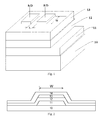
- the first concave-and-convex structure may comprise ridges and troughs arranged alternately in the width direction of the channel region and extending in a length direction of the channel region.
- a width-length ratio of the thin-film transistor can be efficiently increased, an on-current of the thin-film transistor is increased, and power consumption is reduced.
- the thin-film transistor according to the embodiment of the invention and the conventional thin-film transistor have the same width-length ratio, since an effective width of the channel of the thin-film transistor according to the embodiment of the invention is increased, a length of the channel may be reduced, such that an area of the thin-film transistor may be reduced, and in turn, an aperture ratio of a display device can be increased.
- the concave-and-convex structure 121 may be formed on the gate insulation layer 120 first, then the active layer 130 is formed on the gate insulation layer, for example, through a deposition process.
- the concave-and-convex structure 131 can be formed in the surface of the active layer 130 facing the gate insulation layer 120 to match with the shape of the concave-and-convex structure 121, without any extra process.
- the corresponding concave-and-convex structure 131' can be easily formed on the surface of the active layer 130' facing the gate insulation layer 120' through deposition or thermal growth of the gate insulation layer 120' and the active layer 130' in a shape matching manner.
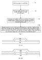
- the method of manufacturing a thin-film transistor comprises the following steps of:
- a gate 110 and a gate insulation layer 120 at least covering the gate 110 are formed successively on a substrate 100 such as a glass substrate; then a photoresist layer 150 covering the gate insulation layer 120 is formed, as shown in Fig. 6B .
- a halftone mask (not shown) is provided.
- a semitransparent portion of the halftone mask corresponds to the channel region of the thin-film transistor to be formed
- a completely transparent portion of the halftone mask corresponds to another region other than the channel region, such as an output end region of the thin-film transistor or a peripheral region of a display device, and in the meantime, with the aid of the halftone mask, a photoetching process and an etching process are performed on the photoresist layer 150 to form a plurality of grooves 151 in a portion of the photoresist layer 150 located in a region corresponding to the channel region CR, and to form a via hole 152 in a portion of the photoresist layer 150 located in the another region to expose the gate insulation layer 120, as shown in Fig.
- a surface of the gate insulation layer 120 facing away from the gate 100 (the surface on which the active layer is to be formed) is formed with a concave-and-convex structure 121 comprising troughs 123 and ridges 124 adjacent thereto.
- the troughs 123 and the ridges 124 are arranged alternately in the width direction of the channel region and extending in the length direction of the channel region.
- the via hole 152 does not need to penetrate through the gate insulation layer, but may only extend in a part of the gate insulation layer, as long as a suitable concave-and-convex structure can be formed in the region corresponding to the channel region.
- a patternized active layer 130 is formed on the gate insulation layer 120 having the concave-and-convex structure 121 through, for example, a deposition process or other suitable semiconductor processes, and in the meantime, in the channel region of the thin-film transistor, the concave-and-convex structure 131 matching with the concave-and-convex structure 121 in shape is formed on the surface of the active layer 130 facing the gate insulation layer 120, the concave-and-convex structure 131 comprises ridges 133 corresponding to the troughs 123 and troughs 134 corresponding to the ridges 124, as shown in Fig. 6F .
- a concave-and-convex structure i.e. a non-planar channel structure, is formed on the surface of the active layer facing the gate insulation layer in the channel region.
- a concave-and-convex structure may also be formed on the surface of the active layer facing the gate insulation layer.
- the method of manufacturing a thin-film transistor may comprise the following steps of:
- a method of manufacturing a top-gate thin-film transistor may comprises the following steps of:
- embodiments of the invention also provide a display substrate comprising a substrate and a thin-film transistor formed on the substrate, the thin-film transistor is the thin-film transistor as described above or the thin-film transistor manufactured through the method as described above.
Landscapes
- Thin Film Transistor (AREA)
Applications Claiming Priority (2)
| Application Number | Priority Date | Filing Date | Title |
|---|---|---|---|
| CN201510063966.4A CN104576761B (zh) | 2015-02-06 | 2015-02-06 | 薄膜晶体管及其制造方法、显示基板和显示装置 |
| PCT/CN2015/085281 WO2016123931A1 (fr) | 2015-02-06 | 2015-07-28 | Transistor à couche mince et son procédé de fabrication, substrat d'affichage et dispositif d'affichage |
Publications (3)
| Publication Number | Publication Date |
|---|---|
| EP3076437A1 true EP3076437A1 (fr) | 2016-10-05 |
| EP3076437A4 EP3076437A4 (fr) | 2017-08-16 |
| EP3076437B1 EP3076437B1 (fr) | 2020-09-02 |
Family
ID=53092399
Family Applications (1)
| Application Number | Title | Priority Date | Filing Date |
|---|---|---|---|
| EP15832664.5A Not-in-force EP3076437B1 (fr) | 2015-02-06 | 2015-07-28 | Transistor à couche mince et son procédé de fabrication |
Country Status (4)
| Country | Link |
|---|---|
| US (1) | US10043916B2 (fr) |
| EP (1) | EP3076437B1 (fr) |
| CN (1) | CN104576761B (fr) |
| WO (1) | WO2016123931A1 (fr) |
Cited By (1)
| Publication number | Priority date | Publication date | Assignee | Title |
|---|---|---|---|---|
| US11417849B2 (en) * | 2019-05-31 | 2022-08-16 | The Regents Of The University Of Colorado, A Body Corporate | Fabrication of corrugated gate dielectric structures using atomic layer etching |
Families Citing this family (18)
| Publication number | Priority date | Publication date | Assignee | Title |
|---|---|---|---|---|
| CN104576761B (zh) * | 2015-02-06 | 2018-05-08 | 合肥京东方光电科技有限公司 | 薄膜晶体管及其制造方法、显示基板和显示装置 |
| CN105097895B (zh) * | 2015-06-25 | 2018-09-21 | 京东方科技集团股份有限公司 | 薄膜晶体管、阵列基板及显示装置 |
| KR102491851B1 (ko) * | 2015-07-02 | 2023-01-26 | 삼성전자주식회사 | 마이크로 구조체를 포함하는 플렉서블 바이모달 센서 |
| KR102537286B1 (ko) * | 2016-07-04 | 2023-05-30 | 삼성디스플레이 주식회사 | 표시 기판 및 이의 제조 방법 |
| CN106784015B (zh) * | 2017-01-03 | 2019-12-03 | 京东方科技集团股份有限公司 | 一种薄膜晶体管及其制作方法、显示基板及显示装置 |
| CN106898614B (zh) * | 2017-02-27 | 2019-09-03 | 京东方科技集团股份有限公司 | 一种柔性阵列基板、显示面板及制作方法 |
| JP2019047026A (ja) * | 2017-09-05 | 2019-03-22 | 株式会社ジャパンディスプレイ | 表示装置 |
| TWI646691B (zh) * | 2017-11-22 | 2019-01-01 | 友達光電股份有限公司 | 主動元件基板及其製造方法 |
| KR102553881B1 (ko) * | 2018-06-01 | 2023-07-07 | 삼성전자주식회사 | 박막 트랜지스터 및 그 제조 방법과 이를 포함하는 박막 트랜지스터 표시판 및 전자 장치 |
| CN110010698B (zh) * | 2019-04-09 | 2022-07-29 | 合肥鑫晟光电科技有限公司 | 薄膜晶体管及其制备方法、显示基板、显示装置 |
| CN110729359A (zh) | 2019-10-25 | 2020-01-24 | 深圳市华星光电半导体显示技术有限公司 | 一种薄膜晶体管、显示面板及薄膜晶体管的制作方法 |
| CN110931514B (zh) * | 2019-11-29 | 2022-04-08 | 云谷(固安)科技有限公司 | 阵列基板和显示面板 |
| CN110993620A (zh) * | 2019-12-05 | 2020-04-10 | 深圳市华星光电半导体显示技术有限公司 | 阵列基板及其制备方法、显示面板 |
| CN114450798B (zh) * | 2020-08-31 | 2025-09-19 | 京东方科技集团股份有限公司 | 显示基板及显示装置 |
| CN114005881B (zh) * | 2021-10-27 | 2023-04-18 | 云谷(固安)科技有限公司 | 薄膜晶体管及其制备方法、像素电路 |
| CN115312540B (zh) * | 2022-07-28 | 2026-04-03 | 武汉华星光电技术有限公司 | 阵列基板及显示面板 |
| CN118676211B (zh) * | 2023-08-31 | 2025-12-02 | 昆山国显光电有限公司 | 薄膜晶体管、薄膜晶体管制备方法及显示面板 |
| CN118983324A (zh) * | 2024-08-05 | 2024-11-19 | 武汉华星光电技术有限公司 | 阵列基板及显示面板 |
Family Cites Families (22)
| Publication number | Priority date | Publication date | Assignee | Title |
|---|---|---|---|---|
| JPS62128177A (ja) * | 1985-11-29 | 1987-06-10 | Toshiba Corp | 薄膜トランジスタ |
| JPH07321129A (ja) * | 1994-05-19 | 1995-12-08 | Japan Energy Corp | 電界効果トランジスタ |
| JPH11177102A (ja) * | 1997-12-08 | 1999-07-02 | Semiconductor Energy Lab Co Ltd | 半導体装置およびその作製方法 |
| US6355532B1 (en) * | 1999-10-06 | 2002-03-12 | Lsi Logic Corporation | Subtractive oxidation method of fabricating a short-length and vertically-oriented channel, dual-gate, CMOS FET |
| KR100764273B1 (ko) * | 2001-05-31 | 2007-10-05 | 비오이 하이디스 테크놀로지 주식회사 | 박막트랜지스터 제조방법 |
| JP4593094B2 (ja) * | 2003-08-21 | 2010-12-08 | 日本電気株式会社 | 液晶表示装置及びその製造方法 |
| KR100703467B1 (ko) * | 2005-01-07 | 2007-04-03 | 삼성에스디아이 주식회사 | 박막트랜지스터 |
| US8110863B2 (en) * | 2005-06-01 | 2012-02-07 | Sandisk 3D Llc | TFT charge storage memory cell having high-mobility corrugated channel |
| TWI300625B (en) * | 2006-05-16 | 2008-09-01 | Ind Tech Res Inst | Structure of semiconductor device and fabrication method |
| KR20090041061A (ko) * | 2007-10-23 | 2009-04-28 | 엘지디스플레이 주식회사 | 박막 트랜지스터 및 그 제조방법 |
| US8436353B2 (en) * | 2008-09-16 | 2013-05-07 | Sharp Kabushiki Kaisha | Thin film transistor with recess |
| JP5477547B2 (ja) * | 2009-06-22 | 2014-04-23 | ソニー株式会社 | 薄膜トランジスタの製造方法 |
| CN202282354U (zh) | 2011-04-21 | 2012-06-20 | 京东方科技集团股份有限公司 | 一种薄膜晶体管及显示装置 |
| JP2013016611A (ja) * | 2011-07-04 | 2013-01-24 | Sony Corp | 半導体装置及びその製造方法、並びに、画像表示装置の製造方法 |
| CN102437196B (zh) * | 2011-12-15 | 2013-04-03 | 昆山工研院新型平板显示技术中心有限公司 | 低温多晶硅薄膜晶体管的制造方法 |
| JP5991668B2 (ja) * | 2012-08-23 | 2016-09-14 | 株式会社ジャパンディスプレイ | 表示装置及びその製造方法 |
| CN102945807B (zh) | 2012-11-15 | 2015-11-25 | 京东方科技集团股份有限公司 | 一种薄膜晶体管的制备方法及薄膜晶体管 |
| CN103165471A (zh) * | 2013-02-19 | 2013-06-19 | 京东方科技集团股份有限公司 | 薄膜晶体管及其制作方法和显示装置 |
| CN103199112B (zh) | 2013-03-20 | 2017-02-15 | 北京京东方光电科技有限公司 | 一种阵列基板及其制备方法和显示面板 |
| CN103762218A (zh) * | 2014-01-16 | 2014-04-30 | 北京京东方光电科技有限公司 | 阵列基板及其制造方法和显示装置 |
| CN103824780B (zh) * | 2014-02-28 | 2016-03-30 | 上海和辉光电有限公司 | 一种低温多晶硅tft器件及其制造方法 |
| CN104576761B (zh) | 2015-02-06 | 2018-05-08 | 合肥京东方光电科技有限公司 | 薄膜晶体管及其制造方法、显示基板和显示装置 |
-
2015
- 2015-02-06 CN CN201510063966.4A patent/CN104576761B/zh not_active Expired - Fee Related
- 2015-07-28 WO PCT/CN2015/085281 patent/WO2016123931A1/fr not_active Ceased
- 2015-07-28 US US14/913,160 patent/US10043916B2/en not_active Expired - Fee Related
- 2015-07-28 EP EP15832664.5A patent/EP3076437B1/fr not_active Not-in-force
Cited By (1)
| Publication number | Priority date | Publication date | Assignee | Title |
|---|---|---|---|---|
| US11417849B2 (en) * | 2019-05-31 | 2022-08-16 | The Regents Of The University Of Colorado, A Body Corporate | Fabrication of corrugated gate dielectric structures using atomic layer etching |
Also Published As
| Publication number | Publication date |
|---|---|
| EP3076437B1 (fr) | 2020-09-02 |
| CN104576761B (zh) | 2018-05-08 |
| CN104576761A (zh) | 2015-04-29 |
| US20160351724A1 (en) | 2016-12-01 |
| US10043916B2 (en) | 2018-08-07 |
| WO2016123931A1 (fr) | 2016-08-11 |
| EP3076437A4 (fr) | 2017-08-16 |
Similar Documents
| Publication | Publication Date | Title |
|---|---|---|
| EP3076437B1 (fr) | Transistor à couche mince et son procédé de fabrication | |
| US8643799B2 (en) | TFT-LCD array substrate and manufacturing method thereof | |
| US9711542B2 (en) | Method for fabricating display panel | |
| US7839462B2 (en) | Pixel structure of liquid crystal display panel and method of making the same | |
| KR101663565B1 (ko) | 액정표시장치 | |
| US9166059B2 (en) | Thin film transistor, array substrate and manufacturing method thereof, and display panel | |
| EP2741135A1 (fr) | Substrat de réseau tft-lcd | |
| US9865623B2 (en) | Array substrate and manufacturing method thereof, and display device | |
| CN106950771B (zh) | 一种阵列基板、显示面板及显示装置 | |
| US20170227803A1 (en) | Array Substrate, Manufacturing Method Thereof, and Display Device | |
| US9274388B2 (en) | Array substrate having common electrode driving interface pattern with slits, and manufacturing method thereof, and liquid crystal display | |
| CN108010920A (zh) | 一种显示面板、显示面板的制作方法及显示装置 | |
| JP2018063348A (ja) | 液晶表示パネルおよび液晶表示装置 | |
| EP3485513B1 (fr) | Substrat de réseau, appareil d'affichage et procédé de fabrication de substrat de réseau | |
| JP6892065B2 (ja) | 表示パネル | |
| US20170139247A1 (en) | Thin Film Transistor Array Substrate, Manufacturing for the Same, and Liquid Crystal Display Panel Having the Same | |
| US20170207252A1 (en) | Array substrate, method for fabricating the same, and display apparatus containing the same | |
| JP2010147351A (ja) | 液晶表示装置及びその製造方法 | |
| US8502946B2 (en) | Array substrate of fringe field switching mode liquid crystal display panel and method of manufacturing the same | |
| US20210118914A1 (en) | Tft array substrate and manufacturing method thereof | |
| CN110007505A (zh) | 显示设备 | |
| US7781268B2 (en) | Array substrate and display panel | |
| US10153305B2 (en) | Array substrate, manufacturing method thereof, and display device | |
| US20060119778A1 (en) | Active matrix display device and method for manufacturing the same | |
| US9423644B2 (en) | Display |
Legal Events
| Date | Code | Title | Description |
|---|---|---|---|
| PUAI | Public reference made under article 153(3) epc to a published international application that has entered the european phase |
Free format text: ORIGINAL CODE: 0009012 |
|
| 17P | Request for examination filed |
Effective date: 20160219 |
|
| AK | Designated contracting states |
Kind code of ref document: A1 Designated state(s): AL AT BE BG CH CY CZ DE DK EE ES FI FR GB GR HR HU IE IS IT LI LT LU LV MC MK MT NL NO PL PT RO RS SE SI SK SM TR |
|
| AX | Request for extension of the european patent |
Extension state: BA ME |
|
| STAA | Information on the status of an ep patent application or granted ep patent |
Free format text: STATUS: REQUEST FOR EXAMINATION WAS MADE |
|
| R17P | Request for examination filed (corrected) |
Effective date: 20160219 |
|
| A4 | Supplementary search report drawn up and despatched |
Effective date: 20170714 |
|
| RIC1 | Information provided on ipc code assigned before grant |
Ipc: H01L 21/311 20060101ALI20170710BHEP Ipc: H01L 21/28 20060101ALI20170710BHEP Ipc: H01L 29/10 20060101ALI20170710BHEP Ipc: H01L 29/786 20060101AFI20170710BHEP Ipc: H01L 29/423 20060101ALI20170710BHEP Ipc: H01L 29/66 20060101ALI20170710BHEP |
|
| DAV | Request for validation of the european patent (deleted) | ||
| DAX | Request for extension of the european patent (deleted) | ||
| STAA | Information on the status of an ep patent application or granted ep patent |
Free format text: STATUS: EXAMINATION IS IN PROGRESS |
|
| 17Q | First examination report despatched |
Effective date: 20190715 |
|
| GRAP | Despatch of communication of intention to grant a patent |
Free format text: ORIGINAL CODE: EPIDOSNIGR1 |
|
| STAA | Information on the status of an ep patent application or granted ep patent |
Free format text: STATUS: GRANT OF PATENT IS INTENDED |
|
| INTG | Intention to grant announced |
Effective date: 20200326 |
|
| GRAS | Grant fee paid |
Free format text: ORIGINAL CODE: EPIDOSNIGR3 |
|
| GRAA | (expected) grant |
Free format text: ORIGINAL CODE: 0009210 |
|
| STAA | Information on the status of an ep patent application or granted ep patent |
Free format text: STATUS: THE PATENT HAS BEEN GRANTED |
|
| AK | Designated contracting states |
Kind code of ref document: B1 Designated state(s): AL AT BE BG CH CY CZ DE DK EE ES FI FR GB GR HR HU IE IS IT LI LT LU LV MC MK MT NL NO PL PT RO RS SE SI SK SM TR |
|
| REG | Reference to a national code |
Ref country code: GB Ref legal event code: FG4D |
|
| REG | Reference to a national code |
Ref country code: AT Ref legal event code: REF Ref document number: 1309822 Country of ref document: AT Kind code of ref document: T Effective date: 20200915 Ref country code: CH Ref legal event code: EP |
|
| REG | Reference to a national code |
Ref country code: DE Ref legal event code: R096 Ref document number: 602015058558 Country of ref document: DE |
|
| REG | Reference to a national code |
Ref country code: IE Ref legal event code: FG4D |
|
| REG | Reference to a national code |
Ref country code: LT Ref legal event code: MG4D |
|
| PG25 | Lapsed in a contracting state [announced via postgrant information from national office to epo] |
Ref country code: FI Free format text: LAPSE BECAUSE OF FAILURE TO SUBMIT A TRANSLATION OF THE DESCRIPTION OR TO PAY THE FEE WITHIN THE PRESCRIBED TIME-LIMIT Effective date: 20200902 Ref country code: HR Free format text: LAPSE BECAUSE OF FAILURE TO SUBMIT A TRANSLATION OF THE DESCRIPTION OR TO PAY THE FEE WITHIN THE PRESCRIBED TIME-LIMIT Effective date: 20200902 Ref country code: SE Free format text: LAPSE BECAUSE OF FAILURE TO SUBMIT A TRANSLATION OF THE DESCRIPTION OR TO PAY THE FEE WITHIN THE PRESCRIBED TIME-LIMIT Effective date: 20200902 Ref country code: NO Free format text: LAPSE BECAUSE OF FAILURE TO SUBMIT A TRANSLATION OF THE DESCRIPTION OR TO PAY THE FEE WITHIN THE PRESCRIBED TIME-LIMIT Effective date: 20201202 Ref country code: GR Free format text: LAPSE BECAUSE OF FAILURE TO SUBMIT A TRANSLATION OF THE DESCRIPTION OR TO PAY THE FEE WITHIN THE PRESCRIBED TIME-LIMIT Effective date: 20201203 Ref country code: LT Free format text: LAPSE BECAUSE OF FAILURE TO SUBMIT A TRANSLATION OF THE DESCRIPTION OR TO PAY THE FEE WITHIN THE PRESCRIBED TIME-LIMIT Effective date: 20200902 Ref country code: BG Free format text: LAPSE BECAUSE OF FAILURE TO SUBMIT A TRANSLATION OF THE DESCRIPTION OR TO PAY THE FEE WITHIN THE PRESCRIBED TIME-LIMIT Effective date: 20201202 |
|
| REG | Reference to a national code |
Ref country code: NL Ref legal event code: MP Effective date: 20200902 |
|
| REG | Reference to a national code |
Ref country code: AT Ref legal event code: MK05 Ref document number: 1309822 Country of ref document: AT Kind code of ref document: T Effective date: 20200902 |
|
| PG25 | Lapsed in a contracting state [announced via postgrant information from national office to epo] |
Ref country code: PL Free format text: LAPSE BECAUSE OF FAILURE TO SUBMIT A TRANSLATION OF THE DESCRIPTION OR TO PAY THE FEE WITHIN THE PRESCRIBED TIME-LIMIT Effective date: 20200902 Ref country code: RS Free format text: LAPSE BECAUSE OF FAILURE TO SUBMIT A TRANSLATION OF THE DESCRIPTION OR TO PAY THE FEE WITHIN THE PRESCRIBED TIME-LIMIT Effective date: 20200902 Ref country code: LV Free format text: LAPSE BECAUSE OF FAILURE TO SUBMIT A TRANSLATION OF THE DESCRIPTION OR TO PAY THE FEE WITHIN THE PRESCRIBED TIME-LIMIT Effective date: 20200902 |
|
| PG25 | Lapsed in a contracting state [announced via postgrant information from national office to epo] |
Ref country code: NL Free format text: LAPSE BECAUSE OF FAILURE TO SUBMIT A TRANSLATION OF THE DESCRIPTION OR TO PAY THE FEE WITHIN THE PRESCRIBED TIME-LIMIT Effective date: 20200902 Ref country code: EE Free format text: LAPSE BECAUSE OF FAILURE TO SUBMIT A TRANSLATION OF THE DESCRIPTION OR TO PAY THE FEE WITHIN THE PRESCRIBED TIME-LIMIT Effective date: 20200902 Ref country code: SM Free format text: LAPSE BECAUSE OF FAILURE TO SUBMIT A TRANSLATION OF THE DESCRIPTION OR TO PAY THE FEE WITHIN THE PRESCRIBED TIME-LIMIT Effective date: 20200902 Ref country code: PT Free format text: LAPSE BECAUSE OF FAILURE TO SUBMIT A TRANSLATION OF THE DESCRIPTION OR TO PAY THE FEE WITHIN THE PRESCRIBED TIME-LIMIT Effective date: 20210104 Ref country code: RO Free format text: LAPSE BECAUSE OF FAILURE TO SUBMIT A TRANSLATION OF THE DESCRIPTION OR TO PAY THE FEE WITHIN THE PRESCRIBED TIME-LIMIT Effective date: 20200902 Ref country code: CZ Free format text: LAPSE BECAUSE OF FAILURE TO SUBMIT A TRANSLATION OF THE DESCRIPTION OR TO PAY THE FEE WITHIN THE PRESCRIBED TIME-LIMIT Effective date: 20200902 |
|
| PG25 | Lapsed in a contracting state [announced via postgrant information from national office to epo] |
Ref country code: IS Free format text: LAPSE BECAUSE OF FAILURE TO SUBMIT A TRANSLATION OF THE DESCRIPTION OR TO PAY THE FEE WITHIN THE PRESCRIBED TIME-LIMIT Effective date: 20210102 Ref country code: ES Free format text: LAPSE BECAUSE OF FAILURE TO SUBMIT A TRANSLATION OF THE DESCRIPTION OR TO PAY THE FEE WITHIN THE PRESCRIBED TIME-LIMIT Effective date: 20200902 Ref country code: AT Free format text: LAPSE BECAUSE OF FAILURE TO SUBMIT A TRANSLATION OF THE DESCRIPTION OR TO PAY THE FEE WITHIN THE PRESCRIBED TIME-LIMIT Effective date: 20200902 Ref country code: AL Free format text: LAPSE BECAUSE OF FAILURE TO SUBMIT A TRANSLATION OF THE DESCRIPTION OR TO PAY THE FEE WITHIN THE PRESCRIBED TIME-LIMIT Effective date: 20200902 |
|
| REG | Reference to a national code |
Ref country code: DE Ref legal event code: R097 Ref document number: 602015058558 Country of ref document: DE |
|
| PG25 | Lapsed in a contracting state [announced via postgrant information from national office to epo] |
Ref country code: SK Free format text: LAPSE BECAUSE OF FAILURE TO SUBMIT A TRANSLATION OF THE DESCRIPTION OR TO PAY THE FEE WITHIN THE PRESCRIBED TIME-LIMIT Effective date: 20200902 |
|
| PLBE | No opposition filed within time limit |
Free format text: ORIGINAL CODE: 0009261 |
|
| STAA | Information on the status of an ep patent application or granted ep patent |
Free format text: STATUS: NO OPPOSITION FILED WITHIN TIME LIMIT |
|
| 26N | No opposition filed |
Effective date: 20210603 |
|
| PG25 | Lapsed in a contracting state [announced via postgrant information from national office to epo] |
Ref country code: SI Free format text: LAPSE BECAUSE OF FAILURE TO SUBMIT A TRANSLATION OF THE DESCRIPTION OR TO PAY THE FEE WITHIN THE PRESCRIBED TIME-LIMIT Effective date: 20200902 Ref country code: DK Free format text: LAPSE BECAUSE OF FAILURE TO SUBMIT A TRANSLATION OF THE DESCRIPTION OR TO PAY THE FEE WITHIN THE PRESCRIBED TIME-LIMIT Effective date: 20200902 |
|
| PG25 | Lapsed in a contracting state [announced via postgrant information from national office to epo] |
Ref country code: IT Free format text: LAPSE BECAUSE OF FAILURE TO SUBMIT A TRANSLATION OF THE DESCRIPTION OR TO PAY THE FEE WITHIN THE PRESCRIBED TIME-LIMIT Effective date: 20200902 |
|
| REG | Reference to a national code |
Ref country code: DE Ref legal event code: R119 Ref document number: 602015058558 Country of ref document: DE |
|
| REG | Reference to a national code |
Ref country code: CH Ref legal event code: PL |
|
| GBPC | Gb: european patent ceased through non-payment of renewal fee |
Effective date: 20210728 |
|
| PG25 | Lapsed in a contracting state [announced via postgrant information from national office to epo] |
Ref country code: MC Free format text: LAPSE BECAUSE OF FAILURE TO SUBMIT A TRANSLATION OF THE DESCRIPTION OR TO PAY THE FEE WITHIN THE PRESCRIBED TIME-LIMIT Effective date: 20200902 |
|
| REG | Reference to a national code |
Ref country code: BE Ref legal event code: MM Effective date: 20210731 |
|
| PG25 | Lapsed in a contracting state [announced via postgrant information from national office to epo] |
Ref country code: LI Free format text: LAPSE BECAUSE OF NON-PAYMENT OF DUE FEES Effective date: 20210731 Ref country code: GB Free format text: LAPSE BECAUSE OF NON-PAYMENT OF DUE FEES Effective date: 20210728 Ref country code: DE Free format text: LAPSE BECAUSE OF NON-PAYMENT OF DUE FEES Effective date: 20220201 Ref country code: CH Free format text: LAPSE BECAUSE OF NON-PAYMENT OF DUE FEES Effective date: 20210731 |
|
| PG25 | Lapsed in a contracting state [announced via postgrant information from national office to epo] |
Ref country code: FR Free format text: LAPSE BECAUSE OF NON-PAYMENT OF DUE FEES Effective date: 20210731 Ref country code: LU Free format text: LAPSE BECAUSE OF NON-PAYMENT OF DUE FEES Effective date: 20210728 |
|
| PG25 | Lapsed in a contracting state [announced via postgrant information from national office to epo] |
Ref country code: IE Free format text: LAPSE BECAUSE OF NON-PAYMENT OF DUE FEES Effective date: 20210728 Ref country code: BE Free format text: LAPSE BECAUSE OF NON-PAYMENT OF DUE FEES Effective date: 20210731 |
|
| PG25 | Lapsed in a contracting state [announced via postgrant information from national office to epo] |
Ref country code: HU Free format text: LAPSE BECAUSE OF FAILURE TO SUBMIT A TRANSLATION OF THE DESCRIPTION OR TO PAY THE FEE WITHIN THE PRESCRIBED TIME-LIMIT; INVALID AB INITIO Effective date: 20150728 |
|
| PG25 | Lapsed in a contracting state [announced via postgrant information from national office to epo] |
Ref country code: CY Free format text: LAPSE BECAUSE OF FAILURE TO SUBMIT A TRANSLATION OF THE DESCRIPTION OR TO PAY THE FEE WITHIN THE PRESCRIBED TIME-LIMIT Effective date: 20200902 |
|
| PG25 | Lapsed in a contracting state [announced via postgrant information from national office to epo] |
Ref country code: MK Free format text: LAPSE BECAUSE OF FAILURE TO SUBMIT A TRANSLATION OF THE DESCRIPTION OR TO PAY THE FEE WITHIN THE PRESCRIBED TIME-LIMIT Effective date: 20200902 |
|
| PG25 | Lapsed in a contracting state [announced via postgrant information from national office to epo] |
Ref country code: TR Free format text: LAPSE BECAUSE OF FAILURE TO SUBMIT A TRANSLATION OF THE DESCRIPTION OR TO PAY THE FEE WITHIN THE PRESCRIBED TIME-LIMIT Effective date: 20200902 |
|
| PG25 | Lapsed in a contracting state [announced via postgrant information from national office to epo] |
Ref country code: MT Free format text: LAPSE BECAUSE OF FAILURE TO SUBMIT A TRANSLATION OF THE DESCRIPTION OR TO PAY THE FEE WITHIN THE PRESCRIBED TIME-LIMIT Effective date: 20200902 |