EP3079249A2 - Schema auf basis von konstanter planmässiger impulsbreitensteuerung in spannungswandler - Google Patents
Schema auf basis von konstanter planmässiger impulsbreitensteuerung in spannungswandler Download PDFInfo
- Publication number
- EP3079249A2 EP3079249A2 EP16153775.8A EP16153775A EP3079249A2 EP 3079249 A2 EP3079249 A2 EP 3079249A2 EP 16153775 A EP16153775 A EP 16153775A EP 3079249 A2 EP3079249 A2 EP 3079249A2
- Authority
- EP
- European Patent Office
- Prior art keywords
- signal
- voltage
- output
- pulse width
- current
- Prior art date
- Legal status (The legal status is an assumption and is not a legal conclusion. Google has not performed a legal analysis and makes no representation as to the accuracy of the status listed.)
- Ceased
Links
- 238000003079 width control Methods 0.000 title claims abstract description 20
- 239000003990 capacitor Substances 0.000 claims abstract description 38
- 238000000034 method Methods 0.000 claims description 3
- 238000005070 sampling Methods 0.000 claims description 3
- 238000010586 diagram Methods 0.000 description 12
- 230000036039 immunity Effects 0.000 description 4
- 230000001052 transient effect Effects 0.000 description 3
- 230000003247 decreasing effect Effects 0.000 description 2
- 238000001514 detection method Methods 0.000 description 1
Images




Classifications
-
- H—ELECTRICITY
- H02—GENERATION; CONVERSION OR DISTRIBUTION OF ELECTRIC POWER
- H02M—APPARATUS FOR CONVERSION BETWEEN AC AND AC, BETWEEN AC AND DC, OR BETWEEN DC AND DC, AND FOR USE WITH MAINS OR SIMILAR POWER SUPPLY SYSTEMS; CONVERSION OF DC OR AC INPUT POWER INTO SURGE OUTPUT POWER; CONTROL OR REGULATION THEREOF
- H02M3/00—Conversion of DC power input into DC power output
- H02M3/02—Conversion of DC power input into DC power output without intermediate conversion into AC
- H02M3/04—Conversion of DC power input into DC power output without intermediate conversion into AC by static converters
- H02M3/10—Conversion of DC power input into DC power output without intermediate conversion into AC by static converters using discharge tubes with control electrode or semiconductor devices with control electrode
- H02M3/145—Conversion of DC power input into DC power output without intermediate conversion into AC by static converters using discharge tubes with control electrode or semiconductor devices with control electrode using devices of a triode or transistor type requiring continuous application of a control signal
- H02M3/155—Conversion of DC power input into DC power output without intermediate conversion into AC by static converters using discharge tubes with control electrode or semiconductor devices with control electrode using devices of a triode or transistor type requiring continuous application of a control signal using semiconductor devices only
- H02M3/156—Conversion of DC power input into DC power output without intermediate conversion into AC by static converters using discharge tubes with control electrode or semiconductor devices with control electrode using devices of a triode or transistor type requiring continuous application of a control signal using semiconductor devices only with automatic control of output voltage or current, e.g. switching regulators
- H02M3/158—Conversion of DC power input into DC power output without intermediate conversion into AC by static converters using discharge tubes with control electrode or semiconductor devices with control electrode using devices of a triode or transistor type requiring continuous application of a control signal using semiconductor devices only with automatic control of output voltage or current, e.g. switching regulators including plural semiconductor devices as final control devices for a single load
-
- H—ELECTRICITY
- H02—GENERATION; CONVERSION OR DISTRIBUTION OF ELECTRIC POWER
- H02M—APPARATUS FOR CONVERSION BETWEEN AC AND AC, BETWEEN AC AND DC, OR BETWEEN DC AND DC, AND FOR USE WITH MAINS OR SIMILAR POWER SUPPLY SYSTEMS; CONVERSION OF DC OR AC INPUT POWER INTO SURGE OUTPUT POWER; CONTROL OR REGULATION THEREOF
- H02M3/00—Conversion of DC power input into DC power output
- H02M3/02—Conversion of DC power input into DC power output without intermediate conversion into AC
- H02M3/04—Conversion of DC power input into DC power output without intermediate conversion into AC by static converters
- H02M3/10—Conversion of DC power input into DC power output without intermediate conversion into AC by static converters using discharge tubes with control electrode or semiconductor devices with control electrode
- H02M3/145—Conversion of DC power input into DC power output without intermediate conversion into AC by static converters using discharge tubes with control electrode or semiconductor devices with control electrode using devices of a triode or transistor type requiring continuous application of a control signal
- H02M3/155—Conversion of DC power input into DC power output without intermediate conversion into AC by static converters using discharge tubes with control electrode or semiconductor devices with control electrode using devices of a triode or transistor type requiring continuous application of a control signal using semiconductor devices only
- H02M3/156—Conversion of DC power input into DC power output without intermediate conversion into AC by static converters using discharge tubes with control electrode or semiconductor devices with control electrode using devices of a triode or transistor type requiring continuous application of a control signal using semiconductor devices only with automatic control of output voltage or current, e.g. switching regulators
-
- H—ELECTRICITY
- H02—GENERATION; CONVERSION OR DISTRIBUTION OF ELECTRIC POWER
- H02M—APPARATUS FOR CONVERSION BETWEEN AC AND AC, BETWEEN AC AND DC, OR BETWEEN DC AND DC, AND FOR USE WITH MAINS OR SIMILAR POWER SUPPLY SYSTEMS; CONVERSION OF DC OR AC INPUT POWER INTO SURGE OUTPUT POWER; CONTROL OR REGULATION THEREOF
- H02M1/00—Details of apparatus for conversion
- H02M1/08—Circuits specially adapted for the generation of control voltages for semiconductor devices incorporated in static converters
-
- H—ELECTRICITY
- H02—GENERATION; CONVERSION OR DISTRIBUTION OF ELECTRIC POWER
- H02M—APPARATUS FOR CONVERSION BETWEEN AC AND AC, BETWEEN AC AND DC, OR BETWEEN DC AND DC, AND FOR USE WITH MAINS OR SIMILAR POWER SUPPLY SYSTEMS; CONVERSION OF DC OR AC INPUT POWER INTO SURGE OUTPUT POWER; CONTROL OR REGULATION THEREOF
- H02M1/00—Details of apparatus for conversion
- H02M1/0003—Details of control, feedback or regulation circuits
- H02M1/0009—Devices or circuits for detecting current in a converter
Definitions
- the present invention relates to a voltage converter scheme, and more particularly to a constant on-time pulse width control-based apparatus used in a voltage converter according to the pre-characterizing clauses of claims 1 and 10.
- a conventional constant on-time controller is usually limited by small ESR (equivalent series resistor) of its output capacitor.
- the conventional controller cannot effectively reflect/detect output voltage ripple due to that the ESR is too small.
- Some conventional schemes are proposed to improve the detection of output voltage ripple.
- a part of these conventional schemes cannot improve poor noise immunity and worse DC voltage regulation, and its signal gain for compensation is too low.
- another part of the conventional schemes may further limit the transient response.
- another part of the conventional schemes may adopt a voltage mode control loop and necessarily needs a complicated compensation circuit design due to that it lacks of the current signal for its voltage mode control loop.
- one of the objectives of the present invention is to provide a constant on-time pulse width control-based apparatus used in a voltage converter especially a DC-to-Dc buck converter, to solve the above-mentioned problems.
- a constant on-time pulse width control-based apparatus used in a voltage converter comprise a controller, a comparator, and a logic circuit.
- the comparator is configured for generating a logic control signal to the logic circuit according to two resultant signals of the controller.
- the logic circuit is coupled to the comparator and configured for generating a pulse control signal with an on-time pulse width to charge an output capacitor of an output stage circuit of the voltage converter according to the logic control signal.
- the controller is coupled to the comparator and the logic circuit, and configured for generating the two resultant signals to the comparator by detecting an inductor current signal from an inductor of the output stage circuit, generating a voltage ramp signal, amplifying and generating an output voltage ripple signal based on a reference voltage.
- a constant on-time pulse width control-based method used in a voltage converter comprises: using a comparator to generate a logic control signal according to two resultant signals of a controller; generating a pulse control signal with an on-time pulse width to charge an output capacitor of the voltage converter according to the logic control signal; and, using the controller to generate the two resultant signals to the comparator by detecting an inductor current signal from an inductor of the output stage circuit, generating a voltage ramp signal, amplifying and generating an output voltage ripple signal based on a reference voltage.
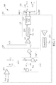
- FIG. 1 is a diagram of a voltage converter 100 according to a first embodiment of the present invention.
- the voltage converter 100 in this embodiment is a DC-to-Dc buck converter (but not limited) and comprises an apparatus 103 and an output stage circuit 120 wherein the apparatus 103 comprises a controller 105, a comparator 110, and a logic circuit 115.
- the controller 105 comprises an error amplifier 1051, a high gain compensator 1053, a current sense circuit 1055, and a voltage ramp generator 1057.
- the logic circuit 115 comprises a generator 1151 and control logic 1153.
- the output stage circuit 120 comprises two switching transistors HSFET & LSFET, an output inductor Lout, and an output capacitor Cout.
- the DC-to-DC buck converter 100 is arranged for receiving an input DC voltage Vin to generating and outputting an output DC voltage Vout.
- the apparatus 103 generates the pulse width control signal Ton to control ON/OFF statuses of the switching transistors HSFET & LSFET to dynamically charge the capacitor Cout during an on-time pulse width of signal Ton, and controls the capacitor Cout to be discharged during an off-time pulse width of Ton.
- the apparatus 103 includes a constant on-time pulse width control-based operation and can be regarded as a constant on-time pulse width control-based controller.
- the constant on-time pulse width control-based operation means that the apparatus 103 is arranged to adopt a fixed on-time pulse width during each cycle to control the ON/OFF statuses of the switching transistors HSFET & LSFET in a normal loading condition; the on-time pulse width may be extended or decreased if the loading condition is changed.
- Conventional constant on-time controller may be limited by small ESR (equivalent series resistor) of an output capacitor; the conventional controller cannot effectively reflect/detect output voltage ripple due to that the ESR is too small. This causes that the conventional constant on-time controller is without good noise immunity and DC regulation.
- the controller 105 combined with comparator 110 and logic circuit 115 is employed so as to solve the problem and also achieves the flexibility of current mode compensation and retains fast transient response.
- the controller 105 is arranged for generating the two resultant signals VC1 and VC2 to the comparator 110 by detecting an inductor current signal IL from the output inductor Lout, generating a voltage ramp signal Vramp to emulate the pure current ramp, amplifying and generating an output voltage ripple signal to generate the signal VC1 based on a reference voltage Vref and the output voltage signal Vout.
- the comparator 110 is configured for generating a logic control signal Sset to the logic circuit 115 according to two resultant signals VC1 and VC2.
- the logic circuit 115 generates the pulse control signal Ton with on-time pulse width to control the switching transistors HSFET & LSFET according to the logic control signal Sset.
- the error amplifier 1051 is used for amplifying the difference between output voltage signal Vout and reference voltage Vref to generate the output voltage ripple signal as the signal VC1.
- the high gain compensator 1053 is used for compensating the output voltage ripple signal with a high gain to provide loop stability and better DC voltage regulation for the output voltage signal Vout.
- the error amplifier 1052 combined with the high gain compensator 1053 can be regarded as an integrator for accumulating the difference between the output voltage signal Vout and reference voltage Vref to generate the output voltage ripple signal so as to amplify the voltage ripple on the output voltage signal Vout.
- the signal VC1 is transmitted to the positive input of the comparator 110.
- the high gain compensator 1053 comprises resistors R1 & R3 and capacitors C1 & C2.
- the resistor R1 is connected with the first capacitor C1 in series and the resistor R1 and the first capacitor C1 are connected between the negative input and the output of the error amplifier 1051.
- the second capacitor C2 is connected with the resistor R1 and the first capacitor C1 in parallel.
- the output voltage signal Vout passes via the resistor R3 and provided for the error amplifier 1051.
- the error amplifier 1051 with the high gain compensator 1053 can provide good noise immunity, better DC regulation, and improved loop stability.
- the current sense circuit 1055 is used for detecting the inductor current signal IL from the output inductor Lout, and the voltage ramp generator 1057 is used for generating a voltage ramp signal Vramp.
- the controller 105 can emulate the pure current ramp signal as the signal VC2 provided for the comparator 110 based on the voltage ramp signal Vramp and a DC level of the detected inductor current signal IL.
- the voltage ramp generator 1057 comprises a voltage source VS, a current source IS, a capacitor C3, and a switch SW.
- the voltage source VS is used for providing a direct-current voltage level.
- the current source IS provides a specific current.
- the capacitor C3 is connected between the voltage source VS and current source IS in series, and the switch SW is connected with the capacitor C3 in parallel.
- the output node of the voltage ramp generator 1057 is disposed between the current source IS and the capacitor C3.
- the switch SW is controlled according to the pulse control signal Ton.
- the controller 105 controls the switch SW to be closed during the on-time pulse width of signal Ton to provide the direct-current voltage level as the voltage ramp signal Vramp, and controls the switch SW to be open during an off-time pulse width of signal Ton to provide a slowly discharged voltage level as the voltage ramp signal Vramp.
- the voltage ramp signal Vramp is like a triangular wave signal with a specific slope.
- the current sense circuit 1055 comprises a current sense amplifier 1058 and a sample/hold unit 1059.
- the current sense amplifier 1058 is used for sensing and amplifying the output inductor current IL with a gain K, and the sample/hold unit 1059 is used for sampling the level of amplified inductor current IL and holding the level.
- the controller 105 generates the resultant signal VC2 by summing up the voltage ramp signal Vramp and the level VDC outputted from the sample/hold unit 1059 to emulate the pure current ramp signal.
- the comparator 110 outputs a logic high level as its output (i.e. the logic control signal Sset) when the signal VC1 is higher than the signal VC2, and outputs a logic low level as its output when the signal VC1 is lower than the signal VC2.
- the generator 1151 receives the DC input voltage Vin and the reference voltage Vref to generate the pulse control signal Ton with the on-time pulse width according to the logic control signal Sset.
- the control logic 1153 controls the ON/OFF statuses of the switching transistors HSFET & LSFET according to the signal Ton.
- FIG. 2 is a diagram illustrating an example of the signals Vramp, VC2, IL, Ton , and cycle of sample/hold unit 1059 as shown in FIG. 1 .
- the signal Vramp for example is a triangle wave signal and is raised to a high level (the DC voltage VS) for a while when the signal VC1 is higher than the signal VC2 (i.e. the on-time pulse width of signal Ton).
- the signal Vramp is decreased gradually with a slope which is determined by the capacitor C3 and/or current IS.
- the signal VC2 is generated by adding the signal Vramp to the signal VDC.
- IL indicates the waveform of the output inductor signal and actually may include some small variations (i.e.
- Ton is a pulse signal generated by the generator 1151 to control the control logic 1153 and its high logic level indicates the on-time pulse width.
- the sample/hold unit 1059 is used for sampling and holding the peak amplitude of the output inductor current IL as the level of VDC; the sample/hold unit 1059 works immediately after each on-time pulse of signal Ton is ended.
- the controller 105 employs the voltage ramp generator 1057 and current sense circuit 1055 to emulate the pure current ramp signal for the output inductor signal IL. It is flexible to increase the amplitude of the signal Vramp by adjusting the capacitor C3 and/or current IS, to improve noise immunity when the DC-to-DC buck converter 100 operates in the current mode and retains the same current gain.
- FIG. 3 is a diagram illustrating an example of the signals VC2, IL, Ton,and cycles of sample/hold unit 1059 as shown in FIG. 1 when the loading of DC-to-DC buck converter 100 varies.
- the loading of DC-to-DC buck converter 100 varies from a light loading condition to a heavy loading condition, and the voltage ramp generator 1057 and current sense circuit 1055 can successfully emulate the pure current ramp that correspondingly varies with the loading condition of DC-to-DC buck converter 100. That is ,it is suitable for using the voltage ramp generator 1057 and current sense circuit 1055 to effectively emulate the pure current ramp even though the loading of DC-to-DC buck converter 100 varies.
- the DC-to-DC buck converter 100 retains the fast transient response.
- the high gain compensator 1053 can be implemented by a different circuit structure that is not connected to the negative input of error amplifier 1051.
- FIG. 4 is a diagram of the DC-to-DC buck converter 100 according to a second embodiment of the present invention.
- the high gain compensator 1053 comprises the resistor R1 connected with the first capacitor C1 in series and the second capacitor C2.
- the resistor R1 combined with the first capacitor C1 are connected between the output of the error amplifier 1051 and the ground level.
- the second capacitor C2 is connected with the resistor R1 and the first capacitor C1 in parallel. Capacitor C1 is also connected between the output of the error amplifier 1051 and the ground level.
- the error amplifier 1051 combined with the high gain compensator 1053 in the second embodiment can be also regarded as an integrator for accumulating the difference between the reference voltage Vref and output voltage Vout.
- the controller 105 can be arranged to generate the signal VC1 based on the output of error amplifier 1051 and the signal VDC outputted from the sample/hold unit 1059, and to generate the voltage ramp signal Vramp as the signal VC2.
- FIG. 5 shows a diagram of the DC-to-DC buck converter 100 according to a third embodiment of the present invention.
- the controller 105 generates the signal VC1 provided for the comparator 110 by subtracting the direct-current level VDC of the detected inductor current signal IL from the amplified output voltage ripple signal of the error amplifier 1051.
- the high gain compensator 1053 shown in FIG. 5 can also be modified.
- FIG. 6 shows a diagram of the DC-to-DC buck converter 100 according to a fourth embodiment of the present invention.
Landscapes
- Engineering & Computer Science (AREA)
- Power Engineering (AREA)
- Dc-Dc Converters (AREA)
Applications Claiming Priority (2)
| Application Number | Priority Date | Filing Date | Title |
|---|---|---|---|
| US201562145212P | 2015-04-09 | 2015-04-09 | |
| US15/007,228 US9831774B2 (en) | 2015-04-09 | 2016-01-27 | Constant on-time pulse width control-based scheme used in voltage converter |
Publications (2)
| Publication Number | Publication Date |
|---|---|
| EP3079249A2 true EP3079249A2 (de) | 2016-10-12 |
| EP3079249A3 EP3079249A3 (de) | 2016-11-23 |
Family
ID=55275028
Family Applications (1)
| Application Number | Title | Priority Date | Filing Date |
|---|---|---|---|
| EP16153775.8A Ceased EP3079249A3 (de) | 2015-04-09 | 2016-02-02 | Schema auf basis von konstanter planmässiger impulsbreitensteuerung in spannungswandler |
Country Status (3)
| Country | Link |
|---|---|
| US (1) | US9831774B2 (de) |
| EP (1) | EP3079249A3 (de) |
| CN (1) | CN106059292A (de) |
Cited By (4)
| Publication number | Priority date | Publication date | Assignee | Title |
|---|---|---|---|---|
| EP3499699A1 (de) * | 2017-12-18 | 2019-06-19 | STMicroelectronics (Grenoble 2) SAS | Stromzuführung mit partitionierung, und ihr steuerverfahren |
| EP3503393A1 (de) * | 2017-12-22 | 2019-06-26 | Nxp B.V. | System und verfahren zur erzeugung von welligkeitsspannung für einen welligkeitsbasierten gleichstrom-gleichstrom-wandler |
| EP3503392A1 (de) * | 2017-12-21 | 2019-06-26 | NXP USA, Inc. | Welligkeitserzeugungsvorrichtung für einen konstanten zeitabhängigen spannungsregler |
| EP3361615B1 (de) * | 2017-02-09 | 2021-08-11 | Rohm Co., Ltd. | Schaltregler und steuerungsvorrichtung dafür |
Families Citing this family (19)
| Publication number | Priority date | Publication date | Assignee | Title |
|---|---|---|---|---|
| US9831774B2 (en) * | 2015-04-09 | 2017-11-28 | Mediatek Inc. | Constant on-time pulse width control-based scheme used in voltage converter |
| US9954440B2 (en) * | 2016-05-13 | 2018-04-24 | Mediatek Inc. | Controller for DC/DC power converters |
| US10886833B2 (en) | 2016-05-24 | 2021-01-05 | Fairchild Semiconductor Corporation | Inductor current emulation for output current monitoring |
| US9853548B1 (en) * | 2017-02-06 | 2017-12-26 | Alpha And Omega Semiconductor Incorporated | Accurate high-side current emulation with auto-conversion for smart power stage applications |
| US10594209B2 (en) * | 2018-01-25 | 2020-03-17 | Richtek Technology Corporation | Switching power converter circuit and control circuit thereof |
| CN110086324B (zh) * | 2018-01-25 | 2021-05-28 | 立锜科技股份有限公司 | 切换式电源转换电路及其中的控制电路 |
| CN110830011B (zh) * | 2018-08-07 | 2023-03-24 | 瑞昱半导体股份有限公司 | 具有脉宽调整模块的时钟电路 |
| US10784917B2 (en) * | 2018-11-27 | 2020-09-22 | Texas Instruments Incorporated | PSI5 base current sampling in synchronous mode |
| US11171563B2 (en) * | 2019-04-30 | 2021-11-09 | Apple Inc. | Phase regulation in a peak current mode power converter |
| CN112019045B (zh) * | 2019-05-29 | 2021-09-21 | 晶豪科技股份有限公司 | 固定开路时间控制器与使用其的降压变换器器件 |
| KR102809236B1 (ko) * | 2019-07-19 | 2025-05-22 | 매그나칩 반도체 유한회사 | 적분 회로 및 그의 제어방법, 이를 포함하는 장치 |
| US10944322B1 (en) * | 2019-10-24 | 2021-03-09 | Kinetic Technologies | Adaptive on-time DC-to-DC buck regulators with constant switching frequency |
| US11621637B2 (en) | 2020-09-15 | 2023-04-04 | Upi Semiconductor Corp. | Control circuit of power converter |
| CN114389451A (zh) * | 2020-10-21 | 2022-04-22 | 圣邦微电子(北京)股份有限公司 | 开关变换器及其控制电路和控制方法 |
| CN114499123B (zh) | 2020-11-12 | 2025-08-29 | 力智电子股份有限公司 | 电源转换器的控制电路 |
| CN114696606B (zh) * | 2020-12-31 | 2024-11-01 | 圣邦微电子(北京)股份有限公司 | 升降压变换器的斜坡电压生成电路 |
| US12003179B2 (en) * | 2021-10-08 | 2024-06-04 | Infineon Technologies Austria Ag | Power supply and emulated current mode to control generation of an output voltage |
| US12132401B2 (en) * | 2022-02-16 | 2024-10-29 | Halo Microelectronics Intermational | Buck converter and control method |
| CN114785125B (zh) * | 2022-04-12 | 2024-11-15 | 东南大学 | 一种应用于恒定导通时间控制的多相交错电路 |
Citations (4)
| Publication number | Priority date | Publication date | Assignee | Title |
|---|---|---|---|---|
| US20090243580A1 (en) * | 2008-03-27 | 2009-10-01 | Gang Chen | Method of forming a power supply controller and structure therefor |
| US20120038331A1 (en) * | 2010-08-10 | 2012-02-16 | Texas Instruments Incoporated | Systems and Methods of Smooth Light Load Operation in a DC/DC Converter |
| US20140132236A1 (en) * | 2012-11-15 | 2014-05-15 | Microchip Technology Incorporated | Slope Compensation Module |
| US20140266117A1 (en) * | 2013-03-14 | 2014-09-18 | Qualcomm Incorporated | Systems and methods for 100 percent duty cycle in switching regulators |
Family Cites Families (10)
| Publication number | Priority date | Publication date | Assignee | Title |
|---|---|---|---|---|
| US6366070B1 (en) | 2001-07-12 | 2002-04-02 | Analog Devices, Inc. | Switching voltage regulator with dual modulation control scheme |
| US7541795B1 (en) * | 2006-02-09 | 2009-06-02 | National Semiconductor Corporation | Apparatus and method for start-up and over-current protection for a regulator |
| KR20090050318A (ko) * | 2007-11-15 | 2009-05-20 | 삼성전자주식회사 | 펄스 스킵 모드로 자동 전환기능을 가진 전력 변환기 및제어 방법 |
| US7888923B2 (en) | 2009-03-27 | 2011-02-15 | Texas Instruments Incorporated | Dynamic phase manager for multi-phase switching regulators |
| US8395367B2 (en) | 2009-08-05 | 2013-03-12 | Upi Semiconductor Corporation | DC-DC converter with a constant on-time pulse width modulation controller |
| US8879283B2 (en) * | 2009-11-05 | 2014-11-04 | On-Bright Electronics (Shanghai) Co., Ltd. | System and method providing protection in the event of current sensing failure for power converter |
| TWI397244B (zh) | 2010-03-25 | 2013-05-21 | Anpec Electronics Corp | 具內部漣波補償之降壓型電源轉換器 |
| US9325233B2 (en) * | 2014-07-01 | 2016-04-26 | Texas Instruments Incorporated | DC to DC converter and PWM controller with adaptive compensation circuit |
| US9831774B2 (en) * | 2015-04-09 | 2017-11-28 | Mediatek Inc. | Constant on-time pulse width control-based scheme used in voltage converter |
| US9735680B2 (en) * | 2015-07-23 | 2017-08-15 | Mediatek Inc. | Constant on-time pulse width control-based scheme including capabilities of fast transient response and adaptively adjusting on-time pulse width |
-
2016
- 2016-01-27 US US15/007,228 patent/US9831774B2/en active Active
- 2016-02-02 EP EP16153775.8A patent/EP3079249A3/de not_active Ceased
- 2016-04-05 CN CN201610207715.3A patent/CN106059292A/zh active Pending
Patent Citations (4)
| Publication number | Priority date | Publication date | Assignee | Title |
|---|---|---|---|---|
| US20090243580A1 (en) * | 2008-03-27 | 2009-10-01 | Gang Chen | Method of forming a power supply controller and structure therefor |
| US20120038331A1 (en) * | 2010-08-10 | 2012-02-16 | Texas Instruments Incoporated | Systems and Methods of Smooth Light Load Operation in a DC/DC Converter |
| US20140132236A1 (en) * | 2012-11-15 | 2014-05-15 | Microchip Technology Incorporated | Slope Compensation Module |
| US20140266117A1 (en) * | 2013-03-14 | 2014-09-18 | Qualcomm Incorporated | Systems and methods for 100 percent duty cycle in switching regulators |
Cited By (5)
| Publication number | Priority date | Publication date | Assignee | Title |
|---|---|---|---|---|
| EP3361615B1 (de) * | 2017-02-09 | 2021-08-11 | Rohm Co., Ltd. | Schaltregler und steuerungsvorrichtung dafür |
| EP3499699A1 (de) * | 2017-12-18 | 2019-06-19 | STMicroelectronics (Grenoble 2) SAS | Stromzuführung mit partitionierung, und ihr steuerverfahren |
| EP3503392A1 (de) * | 2017-12-21 | 2019-06-26 | NXP USA, Inc. | Welligkeitserzeugungsvorrichtung für einen konstanten zeitabhängigen spannungsregler |
| US10411595B2 (en) | 2017-12-21 | 2019-09-10 | Nxp Usa, Inc. | Ripple generation device and method for a constant on-time voltage regulator |
| EP3503393A1 (de) * | 2017-12-22 | 2019-06-26 | Nxp B.V. | System und verfahren zur erzeugung von welligkeitsspannung für einen welligkeitsbasierten gleichstrom-gleichstrom-wandler |
Also Published As
| Publication number | Publication date |
|---|---|
| US20160301307A1 (en) | 2016-10-13 |
| CN106059292A (zh) | 2016-10-26 |
| US9831774B2 (en) | 2017-11-28 |
| EP3079249A3 (de) | 2016-11-23 |
Similar Documents
| Publication | Publication Date | Title |
|---|---|---|
| US9831774B2 (en) | Constant on-time pulse width control-based scheme used in voltage converter | |
| US9735680B2 (en) | Constant on-time pulse width control-based scheme including capabilities of fast transient response and adaptively adjusting on-time pulse width | |
| US9391511B2 (en) | Fast response control circuit and control method thereof | |
| US11303212B2 (en) | Peak-buck peak-boost current-mode control for switched step-up step-down regulators | |
| US8269472B2 (en) | Control circuit and method for a buck-boost power converter | |
| US9154031B2 (en) | Current mode DC-DC conversion device with fast transient response | |
| TWI410033B (zh) | 穩定轉換脈波調變模式之電流式降壓轉換器 | |
| TWI496402B (zh) | 電流式降壓轉換器及使用其之電子系統 | |
| US9716432B2 (en) | Switching converter with constant on-time controller thereof | |
| US8570020B2 (en) | Frequency control circuit and method for a non-constant frequency voltage regulator | |
| TWI395082B (zh) | 用於變頻式電壓調節器的頻率控制電路及方法 | |
| JP5507980B2 (ja) | スイッチング電源の制御回路、電子機器、及びスイッチング電源の制御方法 | |
| US20100231272A1 (en) | Buck-boost power converter with feed-forward technique for achieving fast line response | |
| JP5810298B2 (ja) | スイッチング電源装置 | |
| CN102377344A (zh) | 开关电源装置 | |
| CN102377337A (zh) | 开关电源装置 | |
| CN102281001A (zh) | 开关电源装置 | |
| KR101742760B1 (ko) | 직류-직류 변환기 | |
| CN104297553A (zh) | 输出电压检测电路、控制电路和开关型变换器 | |
| CN112865525A (zh) | 自适应频率调整系统 | |
| CN102377343B (zh) | 固定工作时间切换式直流电源供应器及其控制电路及方法 | |
| EP3002860B1 (de) | Peak-buck-peak-boost-current-mode-steuerung für geschaltete aufwärts-abwärts-regler | |
| CN112448578B (zh) | 开关电源电路 | |
| CN101882872A (zh) | 电流模式dc-dc转换器 | |
| TWI403079B (zh) | 抗雜訊切換式轉換電路及其控制器 |
Legal Events
| Date | Code | Title | Description |
|---|---|---|---|
| PUAI | Public reference made under article 153(3) epc to a published international application that has entered the european phase |
Free format text: ORIGINAL CODE: 0009012 |
|
| AK | Designated contracting states |
Kind code of ref document: A2 Designated state(s): AL AT BE BG CH CY CZ DE DK EE ES FI FR GB GR HR HU IE IS IT LI LT LU LV MC MK MT NL NO PL PT RO RS SE SI SK SM TR |
|
| AX | Request for extension of the european patent |
Extension state: BA ME |
|
| PUAL | Search report despatched |
Free format text: ORIGINAL CODE: 0009013 |
|
| AK | Designated contracting states |
Kind code of ref document: A3 Designated state(s): AL AT BE BG CH CY CZ DE DK EE ES FI FR GB GR HR HU IE IS IT LI LT LU LV MC MK MT NL NO PL PT RO RS SE SI SK SM TR |
|
| AX | Request for extension of the european patent |
Extension state: BA ME |
|
| RIC1 | Information provided on ipc code assigned before grant |
Ipc: H02M 1/08 20060101ALI20161019BHEP Ipc: H02M 3/156 20060101AFI20161019BHEP |
|
| 17P | Request for examination filed |
Effective date: 20170207 |
|
| RBV | Designated contracting states (corrected) |
Designated state(s): AL AT BE BG CH CY CZ DE DK EE ES FI FR GB GR HR HU IE IS IT LI LT LU LV MC MK MT NL NO PL PT RO RS SE SI SK SM TR |
|
| 17Q | First examination report despatched |
Effective date: 20170706 |
|
| STAA | Information on the status of an ep patent application or granted ep patent |
Free format text: STATUS: THE APPLICATION HAS BEEN REFUSED |
|
| 18R | Application refused |
Effective date: 20180903 |