EP3082249A1 - Dispositif de commande de moteur et procédé de commande de moteur - Google Patents
Dispositif de commande de moteur et procédé de commande de moteur Download PDFInfo
- Publication number
- EP3082249A1 EP3082249A1 EP14869826.9A EP14869826A EP3082249A1 EP 3082249 A1 EP3082249 A1 EP 3082249A1 EP 14869826 A EP14869826 A EP 14869826A EP 3082249 A1 EP3082249 A1 EP 3082249A1
- Authority
- EP
- European Patent Office
- Prior art keywords
- ripple current
- output terminal
- voltage side
- magnitude
- inverter circuit
- Prior art date
- Legal status (The legal status is an assumption and is not a legal conclusion. Google has not performed a legal analysis and makes no representation as to the accuracy of the status listed.)
- Granted
Links
Images




Classifications
-
- H—ELECTRICITY
- H02—GENERATION; CONVERSION OR DISTRIBUTION OF ELECTRIC POWER
- H02P—CONTROL OR REGULATION OF ELECTRIC MOTORS, ELECTRIC GENERATORS OR DYNAMO-ELECTRIC CONVERTERS; CONTROLLING TRANSFORMERS, REACTORS OR CHOKE COILS
- H02P6/00—Arrangements for controlling synchronous motors or other dynamo-electric motors using electronic commutation dependent on the rotor position; Electronic commutators therefor
- H02P6/10—Arrangements for controlling torque ripple, e.g. providing reduced torque ripple
-
- H—ELECTRICITY
- H02—GENERATION; CONVERSION OR DISTRIBUTION OF ELECTRIC POWER
- H02P—CONTROL OR REGULATION OF ELECTRIC MOTORS, ELECTRIC GENERATORS OR DYNAMO-ELECTRIC CONVERTERS; CONTROLLING TRANSFORMERS, REACTORS OR CHOKE COILS
- H02P27/00—Arrangements or methods for the control of AC motors characterised by the kind of supply voltage
- H02P27/04—Arrangements or methods for the control of AC motors characterised by the kind of supply voltage using variable-frequency supply voltage, e.g. inverter or converter supply voltage
- H02P27/06—Arrangements or methods for the control of AC motors characterised by the kind of supply voltage using variable-frequency supply voltage, e.g. inverter or converter supply voltage using DC to AC converters or inverters
- H02P27/08—Arrangements or methods for the control of AC motors characterised by the kind of supply voltage using variable-frequency supply voltage, e.g. inverter or converter supply voltage using DC to AC converters or inverters with pulse width modulation
-
- H—ELECTRICITY
- H02—GENERATION; CONVERSION OR DISTRIBUTION OF ELECTRIC POWER
- H02P—CONTROL OR REGULATION OF ELECTRIC MOTORS, ELECTRIC GENERATORS OR DYNAMO-ELECTRIC CONVERTERS; CONTROLLING TRANSFORMERS, REACTORS OR CHOKE COILS
- H02P29/00—Arrangements for regulating or controlling electric motors, appropriate for both AC and DC motors
- H02P29/60—Controlling or determining the temperature of the motor or of the drive
- H02P29/68—Controlling or determining the temperature of the motor or of the drive based on the temperature of a drive component or a semiconductor component
-
- H—ELECTRICITY
- H02—GENERATION; CONVERSION OR DISTRIBUTION OF ELECTRIC POWER
- H02P—CONTROL OR REGULATION OF ELECTRIC MOTORS, ELECTRIC GENERATORS OR DYNAMO-ELECTRIC CONVERTERS; CONTROLLING TRANSFORMERS, REACTORS OR CHOKE COILS
- H02P6/00—Arrangements for controlling synchronous motors or other dynamo-electric motors using electronic commutation dependent on the rotor position; Electronic commutators therefor
- H02P6/14—Electronic commutators
- H02P6/16—Circuit arrangements for detecting position
- H02P6/18—Circuit arrangements for detecting position without separate position detecting elements
-
- H—ELECTRICITY
- H02—GENERATION; CONVERSION OR DISTRIBUTION OF ELECTRIC POWER
- H02P—CONTROL OR REGULATION OF ELECTRIC MOTORS, ELECTRIC GENERATORS OR DYNAMO-ELECTRIC CONVERTERS; CONTROLLING TRANSFORMERS, REACTORS OR CHOKE COILS
- H02P6/00—Arrangements for controlling synchronous motors or other dynamo-electric motors using electronic commutation dependent on the rotor position; Electronic commutators therefor
- H02P6/14—Electronic commutators
- H02P6/16—Circuit arrangements for detecting position
- H02P6/18—Circuit arrangements for detecting position without separate position detecting elements
- H02P6/182—Circuit arrangements for detecting position without separate position detecting elements using back-emf in windings
Definitions
- the present disclosure relates to a motor control device and a motor control method which controls a brushless DC motor in a PWM manner via an inverter circuit according to a position-sensorless method.
- the period of ringing caused by switching becomes longer than the pulse width of a PWM signal in a control region in which the duty ratio of the PWM signal is decreased when a brushless DC motor is controlled in a pulse width modulation (PWM) manner, and driven according to a position-sensorless method.
- PWM pulse width modulation
- Patent Literature 1 discloses technology (referred to as "balanced-drive switching") by which switching devices positioned on upper and lower arms of energizing phases in an inverter circuit are exclusively ON-OFF controlled so as to suppress a change in neutral point potential and to reduce common mode noise. According to this technology, when switching is not performed, the terminal voltage of a winding contains only an induced voltage. Accordingly, the rotational angle of the rotor can be stably detected even in the control region in which the duty ratio of the PWM signal is decreased.
- Patent Literature 1 Japanese Patent No. 4513863
- a motor control device that controls a brushless DC motor in a PWM control manner using an inverter circuit according to a position-sensorless method, includes: a ripple current estimating device configured to estimate a magnitude of a ripple current based on current flowing through a drive power supply line of the inverter circuit; and a control device.
- the inverter circuit includes a first output terminal and a second output terminal respectively corresponding to two energizing phases of the inverter circuit.
- the control device When the magnitude of the ripple current is less than or equal to a threshold value, the control device performs balanced-drive switching that the first output terminal is repeatedly and alternately connected to a high voltage side and a low voltage side of a drive power supply, and the second output terminal, in an opposite way of the first output terminal, is repeatedly and alternately connected to the low voltage side and the high voltage side of the drive power supply.
- the control device When the magnitude of the ripple current exceeds the threshold value, the control device performs unbalanced-drive switching that the first output terminal is repeatedly and alternately connected to the high voltage side and the low voltage side, and the second output terminal is connected only to the low voltage side.
- a motor control device that controls a brushless DC motor in a PWM control manner using an inverter circuit according to a position-sensorless method, includes: a ripple current estimating device configured to estimate a magnitude of a ripple current based on current flowing through a drive power supply line of the inverter circuit; and a control device.
- the inverter circuit includes a first output terminal and a second output terminal respectively corresponding to two energizing phases of the inverter circuit.
- the control device When the magnitude of the ripple current is less than or equal to a threshold value, the control device performs balanced-drive switching only during a predetermined time period that the first output terminal is repeatedly and alternately connected to a high voltage side and a low voltage side of a drive power supply, and the second output terminal, in an opposite way of the first output terminal, is repeatedly and alternately connected to the low voltage side and the high voltage side of the drive power supply, the predetermined time period being around a zero-cross point including a timing at which an induced voltage generated in a stator winding of the brushless DC motor is changed to pass through the zero-cross point.
- the control device When the magnitude of the ripple current is less than or equal to the threshold value, the control device performs unbalanced-drive switching during a period other than the predetermined time period that the first output terminal is repeatedly and alternately connected to the high voltage side and the low voltage side, and the second output terminal is connected only to the low voltage side. When the magnitude of the ripple current exceeds the threshold value, the control device performs the unbalanced-drive switching during an entire time period.
- a motor control method for controlling a brushless DC motor in a PWM control manner using an inverter circuit according to a position-sensorless method includes: estimating a magnitude of a ripple current based on current flowing through a drive power supply line of the inverter circuit, wherein the inverter circuit includes a first output terminal and a second output terminal respectively corresponding to two energizing phases of the inverter circuit; when the magnitude of the ripple current is less than or equal to a threshold value, performing balanced-drive switching that the first output terminal is repeatedly and alternately connected to a high voltage side and a low voltage side of a drive power supply, and the second output terminal, in an opposite way of the first output terminal, is repeatedly and alternately connected to the low voltage side and the high voltage side of the drive power supply; and when the magnitude of the ripple current exceeds the threshold value, performing unbalanced-drive switching that the first output terminal is repeatedly and alternately connected to the high voltage side and the low voltage side, and the second output terminal
- a motor control method for controlling a brushless DC motor in a PWM control manner using an inverter circuit according to a position-sensorless method includes: estimating a magnitude of a ripple current based on current flowing through a drive power supply line of the inverter circuit, wherein the inverter circuit includes a first output terminal and a second output terminal respectively corresponding to two energizing phases of the inverter circuit; when the magnitude of the ripple current is less than or equal to a threshold value, performing balanced-drive switching only during a predetermined time period that the first output terminal is repeatedly and alternately connected to a high voltage side and a low voltage side of a drive power supply, and the second output terminal, in an opposite way of the first output terminal, is repeatedly and alternately connected to the low voltage side and the high voltage side of the drive power supply, the predetermined time period being around a zero-cross point including a timing at which an induced voltage generated in a stator winding of the brushless DC motor is changed to pass
- an inverter device 1 is configured to be connected to a parallel circuit of a DC power supply (drive power supply) 2 and a smoothing capacitor (electrolytic capacitor) 3 via power supply lines (drive power supply lines) 4a and 4b.
- the inverter device 1 is configured to include a microcomputer (control device) 5 and an inverter circuit 6.
- Stator windings 8U, 8V, and 8W of a brushless DC motor 7 (hereinafter, simply referred to as a motor) are respectively connected to a U phase output terminal, a V phase output terminal, and a W phase output terminal of the inverter circuit 6.
- the respective one ends of the stator windings 8U, 8V, and 8W are connected together (star connection).
- the motor 7 is an air-blowing fan motor mounted in a vehicle.
- the inverter circuit 6 is configured such that six N-channel MOSFETs (switching devices) 9a to 9f are connected to each other in a three-phase bridge configuration.
- a freewheel diode (parasitic diode) is connected between a drain and a source of each N-channel MOSFET 9.
- a resistance element (current detection device) 10 is inserted into the power supply line 4b, and both ends of the resistance element 10 are respectively connected to input terminals of the microcomputer 5.
- the microcomputer 5 includes a load current calculating circuit 11; a ripple current calculating circuit (ripple current estimating device) 12; a control determination circuit (control device) 13; and a switching control circuit (control device) 14.
- the load current calculating circuit 11 includes a built-in A/D converter.
- the load current calculating circuit 11 performs A/D conversion on a terminal voltage V of the resistance element 10, and outputs a result of the conversion to the ripple current calculating circuit 12.
- the ripple current calculating circuit 12 calculates a ripple current contained in a load current I, based on the load current I (current flowing through the resistance element 10) obtained from the terminal voltage V and a duty ratio Duty of PWM control performed by the switching control circuit 14, and outputs the calculated ripple current to the control determination circuit 13.
- the control determination circuit 13 compares the input ripple current with a predetermined threshold value, and outputs a switching signal to the switching control circuit 14 according to a result of the comparison.
- the inverter device 1 compares the terminal voltages of the stator windings 8U, 8V, and 8W of the motor 7 with an imaginary neutral point voltage via comparators (not illustrated), and detects a zero-cross point of an induced voltage.
- An output signal of each phase comparator is input to the switching control circuit 14.
- the switching control circuit 14 generates a phasing signal (position detection signal) indicating a zero-cross timing of each phase based on each of the output signals.
- the switching control circuit 14 switches an energizing pattern for the N-channel MOSFET 9 of the inverter circuit 6 to another pattern based on the phasing signal.
- the switching control circuit 14 generates a PWM signal for each phase by determining a duty ratio of PWM control according to a control command input from an external device, and comparing the duty ratio with the amplitude level of a carrier such as a triangle wave.
- the switching control circuit 14 outputs the PWM signals to gates of the N-channel MOSFETs 9a to 9f via a drive circuit (not illustrated).
- the switching control circuit 14 switches a switching pattern, which is used in PWM control, between balanced-drive switching and unbalanced-drive switching according to the switching signal input from the control determination circuit 13.
- This state is switched to a state in which only the N-channel MOSFETs 9b and 9d are turned on. At this time, current flows through a path from the winding 8U, to the winding 8V, to the N-channel MOSFET 9b, to the smoothing capacitor 3, to the N-channel MOSFET 9d, and then to the winding 8U. That is, the turn-on phases are alternately switched in a sequence of (U+, V-), (U-, V+), (U+, V-), (U-, V+), ...
- a V phase output terminal of the inverter circuit 6 is alternately connected to a negative terminal and a positive terminal of the DC power supply 2 in accordance with when a U phase output terminal of the inverter circuit 6 is alternately connected to the positive terminal and the negative terminal of the DC power supply 2.
- the calculated value of a ripple current indicates a peak value at a duty of 80%. Thereafter, the calculated value is decreased to zero until a duty of 100% is reached, and in contrast, the measured value is only decreased to 4 A (effective value).
- FIG. 4 when current flows through the resistance element (shunt resistor) 10, the voltage V occurs between both ends of the resistance element 10 (S1).
- the flowchart in Fig. 4 illustrates not only a process sequence but also events occurring in time series.
- the microcomputer 4 reads the terminal voltage (shunt voltage) V, performs A/D conversion on the read terminal voltage V (S2), and calculates the load current I by dividing the read terminal voltage V by a resistance value R of the resistance element 10 via the load current calculating circuit 11 (S3).
- the calculated load current I is output to the ripple current calculating circuit 12 (S4).
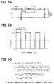
- a ripple current Ir (effective value) occurring in the smoothing capacitor 3 is calculated by the following expression (S5).
- Ir I ⁇ Duty ⁇ 1 ⁇ Duty
- Expression (1) is obtained from an expression for calculating the effective value of a ripple current Icin_rms occurring in an input side capacitor Cin in a model of a step-down DC/DC converter as illustrated in Figs. 5A to 5C .
- a ripple current flowing through an input side coil is negligible.
- the calculated ripple current Ir is output to the control determination circuit 13 (S6).
- the control determination circuit 13 compares the ripple current Ir with a predetermined threshold value, and selects a balanced-drive switching pattern when the ripple current Ir is less than or equal to the threshold value. In contrast, when the ripple current Ir is greater than the threshold value, the control determination circuit 13 selects an unbalanced-drive switching pattern (S7).
- a switching signal according to a selected (determined) switching pattern is output to the switching control circuit 14 (S8).
- the switching control circuit 14 executes either a balanced-drive switching pattern or an unbalanced-drive switching pattern (S9) according to the switching signal.
- a masking period which is used to mask a period during which a freewheeling current flows through a diode of the N-channel MOSFET 9, is started at the edge of a phase signal for each phase which appears every electrical angle of 60 degrees.
- the control switching timing is set to a point in time after the masking period has elapsed (refer to a fourth embodiment for a detailed description of this timing).
- the ripple current calculating circuit 12 of the microcomputer 5 estimates the magnitude of the ripple current Ir contained in current flowing through the power supply line 4b of the inverter circuit 6.
- the switching control circuit 14 performs balanced-drive switching by which one of the output terminals corresponding to two energizing phases, that is, an upper side energizing phase and a lower side energizing phase of the inverter circuit 6 is repeatedly alternately connected to the positive terminal (high voltage side) and the negative terminal (low voltage side) of the DC power supply 2, and the other of the output terminals is repeatedly alternately connected to the negative terminal and the positive terminal.
- the switching control circuit 14 When the magnitude of the ripple current Ir exceeds the threshold value, the switching control circuit 14 performs unbalanced-drive switching by which the one of the output terminals is alternately connected to the high voltage side and the low voltage side, and the other of the output terminals is connected only to the negative terminal.
- the switching control circuit 14 performs switching between the balanced-drive switching and the unbalanced-drive switching synchronously with every electrical angle of 60 degrees at which the energizing pattern for the inverter circuit 6 is switched, the switching pattern can be smoothly switched in accordance with the switching of the energizing pattern.
- the ripple current calculating circuit 12 detects current flowing through the power supply line 4b via the resistance element 10, and estimates the magnitude of the ripple current Ir based on the detected current according to Expression (1). Accordingly, the ripple current Ir can be properly estimated while the duty ratio Duty in PWM control is taken into consideration.
- a diode circuit temperature detection device and ripple current estimating device 22 22 in which multiple diodes are connected in series to each other, is disposed in the vicinity of a smoothing capacitor 3 so as to detect the temperature of the smoothing capacitor 3.
- the diode circuit 22 is connected in series to a current source 23, which is disposed on an anode side of the diode circuit 22, between the power supply and the ground.
- a microcomputer 24 replacing the microcomputer 5 includes a diode temperature calculating circuit (temperature estimating device and ripple current estimating device) 25.
- the diode temperature calculating circuit 25 reads the terminal voltage of the diode circuit 22, that is, a voltage Vf which is a sum of forward voltages of the multiple diodes, and performs A/D conversion on the voltage Vf.
- the diode temperature calculating circuit 25 obtains the internal temperature of the smoothing capacitor 3 based on a result of the conversion according to a conversion expression or the like indicating a correlation between the conversion result and the internal temperature.
- the diode temperature calculating circuit 25 outputs the obtained internal temperature to a ripple current calculating circuit (ripple current estimating device) 26 replacing the ripple current calculating circuit 12.
- the ripple current calculating circuit 26 calculates a ripple current based on the load current I and the voltage Vf, and outputs the calculated ripple current to the control determination circuit 13.
- Steps S1 to S4 illustrated in Fig. 4 are omitted from Fig. 9 ; however, these steps are executed similar to the first embodiment.
- the smoothing capacitor 3 generates heat due to a ripple current flowing thereinto (S11)
- the terminal voltage Vf of the diode circuit (Di) 22 is changed due to the generated heat (S12). That is, the terminal voltage Vf is decreased along with an increase in the temperature of the smoothing capacitor 3.
- the diode temperature calculating circuit 25 When the microcomputer 24 reads the terminal voltage Vf (S13), and estimates the internal temperature of the smoothing capacitor 3 via the diode temperature calculating circuit 25 (S14), the diode temperature calculating circuit 25 outputs the estimated temperature to the ripple current calculating circuit 26 (S15). As described above, the ripple current calculating circuit 26 calculates a ripple current based on the load current I and the voltage Vf (S16), and outputs the calculated ripple current to the control determination circuit 13 (S17). Subsequently, steps S7 to S9 are executed similar to the first embodiment.
- the diode temperature calculating circuit 25 estimates the internal temperature of the smoothing capacitor 3 based on the detected temperature
- the ripple current calculating circuit 26 estimates the magnitude of a ripple current based on the estimated temperature and the load current I. Accordingly, the magnitude of the ripple current can be properly estimated according to the internal temperature of the smoothing capacitor 3.
- a diode used as a temperature detection device is not limited to the diode circuit 22 in which multiple elements are connected in series to each other, and only one element may be used as a diode. However, when the diode circuit 22 including multiple elements is used, a change in the terminal voltage Vf is increased, and thus the accuracy of detecting the temperature is improved.
- a thermistor (temperature detection device and ripple current estimating device) 32 is disposed in the vicinity of a smoothing capacitor 3 so as to detect the temperature of the smoothing capacitor 3.
- the thermistor 32 is connected in series to a resistance element 33 between the power supply and the ground.
- a microcomputer 34 replacing the microcomputer 5 includes a thermistor temperature detecting circuit (temperature estimating device and ripple current estimating device) 35 replacing the diode temperature calculating circuit 25.
- the thermistor temperature calculating circuit 35 reads a terminal voltage Vt of the thermistor 32, and performs A/D conversion on the terminal voltage Vt.
- the thermistor temperature calculating circuit 35 obtains the internal temperature of the smoothing capacitor 3 based on a result of the conversion according to a conversion expression or the like indicating a correlation between the conversion result and the internal temperature.
- the thermistor temperature calculating circuit 35 outputs the obtained internal temperature to the ripple current calculating circuit 26.
- the terminal voltage Vt of the thermistor 32 is changed due to the generated heat (S21). That is, the terminal voltage Vt is decreased along with an increase in the temperature of the smoothing capacitor 3 (when the thermistor 32 has a negative temperature coefficient).
- step S16' is executed similar to the second embodiment (a calculation result of step S24 is used in step S16').
- the thermistor temperature calculating circuit 35 estimates the internal temperature of the smoothing capacitor 3 based on the detected temperature, and the ripple current calculating circuit 26 estimates the magnitude of a ripple current based on the estimated temperature and the load current I. Accordingly, similar to the second embodiment, the magnitude of the ripple current can be properly estimated according to the internal temperature of the smoothing capacitor 3.
- a period for performing balanced-drive switching is reduced.
- a comparator outputs a comparative signal Uc (refer to Fig. 12B ) based on the terminal voltage (refer to Fig. 12A ) of the U-phase stator winding 8U. Correction is performed to remove a freewheeling current period contained in the comparative signal Uc, and a phasing signal Un is generated (refer to Fig. 12C ).
- a timer for measuring the period of an electrical angle of 60 degrees, a timer for determining a commutation timing, a timer for setting a masking period for a freewheeling current period, and the like are operated at the rising edge and the falling edge of a phasing signal for each phase (refer to Fig. 12D ).
- energizing signals for the U phase are generated and output, and as illustrated in Fig. 12E , a balanced-drive switching period when the ripple current Ir is less than or equal to the threshold value is set. That is, in the first embodiment, balanced-drive switching is performed during the entire period in which a ripple current is less than or equal to the threshold value. In contrast, in the fourth embodiment, balanced-drive switching is performed only during a predetermined period around a zero-cross point.
- the down counting of the masking period counter illustrated by the alternate one long and one short dashed line in Fig. 12D is started at a start timing of the period of an electrical angle of 60 degrees.
- a counter value becomes zero
- the masking period is ended, and balanced-drive switching is started.
- a predetermined amount of time based on the counter value of the masking period counter has elapsed after a start timing of the period of an electrical angle of 60 degrees is reached, the balanced-drive switching is ended.
- An execution period of the balanced-drive switching illustrated in Fig. 12E is applied to switching between the V phase and the W phase.
- the bidirectional arrow in Fig. 12E indicates the maximum "predetermined period of time around a zero-cross point, which contains a timing at which an induced voltage is changed to pass through the zero-cross point". That is, the "maximum predetermined period of time” refers to a time period from when a freewheeling current becomes zero to when the energization of the relevant phase is started.
- one purpose of performing balanced-drive switching is to increase a period in which the zero-cross point can be detected, this purpose can be achieved by performing balanced-drive switching only during the predetermined period of time around the zero-cross point.
- the switching pattern is switched to perform unbalanced-drive switching even during the period for performing balanced-drive switching.
- the switching control circuit 12 performs balanced-drive switching, which is performed when the ripple current Ir is less than or equal to the threshold value, only during the predetermined period of time around the zero-cross point, which contains the timing at which an induced voltage occurring in the stator winding 8 of the motor 7 is changed to pass through the zero-cross point.
- the switching control circuit 12 performs unbalanced-drive switching at a period other than the predetermined period of time.
- the switching pattern is switched to perform unbalanced-drive switching during the entire period of time. Accordingly, when the ripple current Ir is low, the period for performing balanced-drive switching is considerably reduced, and thus the increasing period of the ripple current can be reduced while securing the period in which the zero-cross point can be detected.
- the N-channel MOSFET 9d may be turned on during the period in which current flows through the parasitic diode of the N-channel MOSFET 9d. Accordingly, the occurrence of a loss in the parasitic diode can be suppressed.
- a current transformer may be used as a current detection device. The current of the power supply line 4a may be detected.
- the switching pattern may be switched when it is detected that a ripple current exceeds the threshold value.
- a switching device is not limited to an N-channel MOSFET, and a P-channel MOSFET may be used on a positive side.
- a switching device is not limited to a MOSFET, and an IGBT, a bipolar transistor, or the like may be used.
- the present disclosure may be applied to motors other than a fan motor.
- 1 represents an inverter device
- 2 represents a DC power supply (drive power supply)
- 3 represents a smoothing capacitor
- 4 represents a power supply line (drive power supply line)
- 6 represents an inverter circuit
- 7 represents a brushless DC motor
- 10 represents a resistance element (current detection device)
- 12 represents a ripple current calculating circuit (ripple current estimating device)
- 13 represents a control determination circuit (control device)
- 14 represents a switching control circuit (control device).
- a flowchart or the processing of the flowchart in the present application includes sections (also referred to as steps), each of which is represented, for instance, as S1. Further, each section can be divided into several sub-sections while several sections can be combined into a single section. Furthermore, each of thus configured sections can be also referred to as a device, module, or means.
Landscapes
- Engineering & Computer Science (AREA)
- Power Engineering (AREA)
- Control Of Motors That Do Not Use Commutators (AREA)
Applications Claiming Priority (2)
| Application Number | Priority Date | Filing Date | Title |
|---|---|---|---|
| JP2013254968A JP6217369B2 (ja) | 2013-12-10 | 2013-12-10 | モータ制御装置及びモータ制御方法 |
| PCT/JP2014/005902 WO2015087503A1 (fr) | 2013-12-10 | 2014-11-26 | Dispositif de commande de moteur et procédé de commande de moteur |
Publications (3)
| Publication Number | Publication Date |
|---|---|
| EP3082249A1 true EP3082249A1 (fr) | 2016-10-19 |
| EP3082249A4 EP3082249A4 (fr) | 2017-12-13 |
| EP3082249B1 EP3082249B1 (fr) | 2020-06-03 |
Family
ID=53370834
Family Applications (1)
| Application Number | Title | Priority Date | Filing Date |
|---|---|---|---|
| EP14869826.9A Active EP3082249B1 (fr) | 2013-12-10 | 2014-11-26 | Dispositif de commande de moteur et procédé de commande de moteur |
Country Status (5)
| Country | Link |
|---|---|
| US (1) | US9866156B2 (fr) |
| EP (1) | EP3082249B1 (fr) |
| JP (1) | JP6217369B2 (fr) |
| CN (1) | CN105684296B (fr) |
| WO (1) | WO2015087503A1 (fr) |
Families Citing this family (11)
| Publication number | Priority date | Publication date | Assignee | Title |
|---|---|---|---|---|
| JP6493068B2 (ja) * | 2015-07-27 | 2019-04-03 | 株式会社デンソー | モータ制御装置 |
| JP6493067B2 (ja) * | 2015-07-27 | 2019-04-03 | 株式会社デンソー | モータ制御装置 |
| JP6693178B2 (ja) * | 2016-03-07 | 2020-05-13 | 株式会社デンソー | モータ制御装置 |
| JP6776951B2 (ja) * | 2017-03-06 | 2020-10-28 | 株式会社デンソー | 回転電機制御装置、および、これを用いた電動パワーステアリング装置 |
| JP6944646B2 (ja) * | 2017-11-16 | 2021-10-06 | 株式会社ジェイテクト | モータ制御装置 |
| US11799403B2 (en) * | 2017-11-21 | 2023-10-24 | Magna Electronics Inc. | BLDC motor with reduced EMC behavior |
| JP7118699B2 (ja) * | 2018-03-30 | 2022-08-16 | 株式会社マキタ | 電動作業機 |
| JP7272188B2 (ja) * | 2019-09-03 | 2023-05-12 | 株式会社デンソー | 回転電機の制御装置及びプログラム |
| KR102771522B1 (ko) * | 2019-12-16 | 2025-02-20 | 현대자동차주식회사 | 인버터 직류 커패시터의 과온 보호 시스템 및 방법 |
| US11844432B2 (en) | 2020-03-27 | 2023-12-19 | La-Z-Boy Incorporated | Furniture motion control system |
| US11193560B1 (en) | 2020-05-29 | 2021-12-07 | Deere & Company | Work vehicle multi-speed drive assembly with bifurcated clutches |
Family Cites Families (20)
| Publication number | Priority date | Publication date | Assignee | Title |
|---|---|---|---|---|
| JP2800161B2 (ja) | 1989-12-28 | 1998-09-21 | 株式会社 指月電機製作所 | アクティブフィルタ装置 |
| JPH10285989A (ja) | 1997-04-04 | 1998-10-23 | Mitsutoyo Corp | 電流検出装置及び電流制御装置 |
| JP3502566B2 (ja) * | 1999-05-18 | 2004-03-02 | 三菱電機株式会社 | 電力変換装置 |
| US6362586B1 (en) * | 2000-09-15 | 2002-03-26 | General Motors Corporation | Method and device for optimal torque control of a permanent magnet synchronous motor over an extended speed range |
| SG149688A1 (en) * | 2002-02-25 | 2009-02-27 | Daikin Ind Ltd | Motor control method and its apparatus |
| KR101041076B1 (ko) * | 2004-12-17 | 2011-06-13 | 삼성전자주식회사 | 브러시리스 직류모터의 기동제어방법 |
| JP2007174745A (ja) | 2005-12-19 | 2007-07-05 | Jtekt Corp | ブラシレスモータのセンサレス制御方法及びブラシレスモータのセンサレス制御装置 |
| US7593243B2 (en) * | 2006-10-09 | 2009-09-22 | Honeywell International Inc. | Intelligent method for DC bus voltage ripple compensation for power conversion units |
| JP4798075B2 (ja) * | 2007-06-26 | 2011-10-19 | トヨタ自動車株式会社 | モータ駆動システム |
| JP4513863B2 (ja) | 2008-01-09 | 2010-07-28 | 株式会社デンソー | 多相回転機の制御装置 |
| DE102008054487A1 (de) | 2008-01-09 | 2009-07-16 | DENSO CORPORARTION, Kariya-shi | Steuersystem für eine mehrphasige elektrische Drehmaschine |
| US7932691B2 (en) * | 2008-04-22 | 2011-04-26 | GM Global Technology Operations LLC | Permanent magnet motor start-up |
| JP5216449B2 (ja) | 2008-07-07 | 2013-06-19 | 日立オートモティブシステムズ株式会社 | モータ制御装置,電力変換装置及びハイブリッド車両 |
| JP4730420B2 (ja) * | 2008-10-09 | 2011-07-20 | トヨタ自動車株式会社 | モータ駆動装置およびモータ駆動装置の制御方法 |
| IT1392853B1 (it) * | 2008-12-18 | 2012-03-23 | St Microelectronics Srl | Controllo predittivo della corrente nel pilotare un carico in modalità pwm |
| JP4698769B2 (ja) | 2009-08-04 | 2011-06-08 | パナソニック株式会社 | 電力変換装置及び誘導加熱装置 |
| JP2011045209A (ja) * | 2009-08-24 | 2011-03-03 | Panasonic Corp | モータ駆動装置およびモータ駆動方法 |
| JP2011217504A (ja) | 2010-03-31 | 2011-10-27 | Fujitsu General Ltd | モータ駆動装置 |
| JP5652217B2 (ja) | 2011-01-18 | 2015-01-14 | ダイキン工業株式会社 | 電力変換装置 |
| JP5857825B2 (ja) * | 2012-03-20 | 2016-02-10 | 株式会社デンソー | モータ制御装置 |
-
2013
- 2013-12-10 JP JP2013254968A patent/JP6217369B2/ja active Active
-
2014
- 2014-11-26 WO PCT/JP2014/005902 patent/WO2015087503A1/fr not_active Ceased
- 2014-11-26 US US14/916,383 patent/US9866156B2/en active Active
- 2014-11-26 EP EP14869826.9A patent/EP3082249B1/fr active Active
- 2014-11-26 CN CN201480059231.8A patent/CN105684296B/zh active Active
Also Published As
| Publication number | Publication date |
|---|---|
| EP3082249B1 (fr) | 2020-06-03 |
| CN105684296B (zh) | 2018-01-02 |
| US9866156B2 (en) | 2018-01-09 |
| JP2015116007A (ja) | 2015-06-22 |
| JP6217369B2 (ja) | 2017-10-25 |
| EP3082249A4 (fr) | 2017-12-13 |
| CN105684296A (zh) | 2016-06-15 |
| WO2015087503A1 (fr) | 2015-06-18 |
| US20160197567A1 (en) | 2016-07-07 |
Similar Documents
| Publication | Publication Date | Title |
|---|---|---|
| EP3082249B1 (fr) | Dispositif de commande de moteur et procédé de commande de moteur | |
| US9093931B2 (en) | Driving apparatus and stop position detection method | |
| EP3493393B1 (fr) | Commutation de bloc afin de réduire les pertes d'onduleur pour entraînements bldc | |
| US8106622B2 (en) | Control system for multiphase rotary machines | |
| US9692332B2 (en) | Power conversion device | |
| JP6089978B2 (ja) | スイッチトリラクタンスモータのpam駆動装置 | |
| AU2015389306B2 (en) | Step-up device and converter device | |
| JP2018107880A (ja) | 電力変換器制御装置 | |
| JP2010011540A (ja) | モータ制御装置 | |
| JP2004007964A (ja) | 車両用三相回転電機用インバータ回路装置 | |
| CN110870198A (zh) | 驱动装置、控制方法以及程序 | |
| JP5047582B2 (ja) | インバータ装置 | |
| JP6308519B2 (ja) | モータ駆動装置及びモータ制御方法 | |
| US12155331B2 (en) | Motor controller, motor system and method for controlling motor | |
| US10910968B2 (en) | Motor drive device and motor drive system | |
| US20180331639A1 (en) | Motor drive device | |
| JP2012182874A (ja) | モータ制御装置 | |
| EP2523341A2 (fr) | Appareil de détection de position de rotor | |
| JP5330728B2 (ja) | ブラシレスモータの駆動装置 | |
| EP2704308A1 (fr) | Dispositif et procédé de commande de moteur sans balai | |
| US11664755B2 (en) | Arithmetic device and motor drive device | |
| JP6198083B2 (ja) | 電動工具 | |
| JP2007236090A (ja) | ブラシレスモータの制御方法および制御装置 | |
| JP2012191730A (ja) | モータの制御装置 |
Legal Events
| Date | Code | Title | Description |
|---|---|---|---|
| PUAI | Public reference made under article 153(3) epc to a published international application that has entered the european phase |
Free format text: ORIGINAL CODE: 0009012 |
|
| 17P | Request for examination filed |
Effective date: 20160316 |
|
| AK | Designated contracting states |
Kind code of ref document: A1 Designated state(s): AL AT BE BG CH CY CZ DE DK EE ES FI FR GB GR HR HU IE IS IT LI LT LU LV MC MK MT NL NO PL PT RO RS SE SI SK SM TR |
|
| AX | Request for extension of the european patent |
Extension state: BA ME |
|
| DAX | Request for extension of the european patent (deleted) | ||
| A4 | Supplementary search report drawn up and despatched |
Effective date: 20171114 |
|
| RIC1 | Information provided on ipc code assigned before grant |
Ipc: H02P 6/182 20160101ALI20171108BHEP Ipc: H02P 6/10 20060101AFI20171108BHEP Ipc: H02P 29/68 20160101ALI20171108BHEP |
|
| GRAP | Despatch of communication of intention to grant a patent |
Free format text: ORIGINAL CODE: EPIDOSNIGR1 |
|
| STAA | Information on the status of an ep patent application or granted ep patent |
Free format text: STATUS: GRANT OF PATENT IS INTENDED |
|
| INTG | Intention to grant announced |
Effective date: 20200108 |
|
| GRAS | Grant fee paid |
Free format text: ORIGINAL CODE: EPIDOSNIGR3 |
|
| GRAA | (expected) grant |
Free format text: ORIGINAL CODE: 0009210 |
|
| STAA | Information on the status of an ep patent application or granted ep patent |
Free format text: STATUS: THE PATENT HAS BEEN GRANTED |
|
| AK | Designated contracting states |
Kind code of ref document: B1 Designated state(s): AL AT BE BG CH CY CZ DE DK EE ES FI FR GB GR HR HU IE IS IT LI LT LU LV MC MK MT NL NO PL PT RO RS SE SI SK SM TR |
|
| REG | Reference to a national code |
Ref country code: GB Ref legal event code: FG4D |
|
| REG | Reference to a national code |
Ref country code: CH Ref legal event code: EP Ref country code: AT Ref legal event code: REF Ref document number: 1278072 Country of ref document: AT Kind code of ref document: T Effective date: 20200615 |
|
| REG | Reference to a national code |
Ref country code: DE Ref legal event code: R096 Ref document number: 602014066354 Country of ref document: DE |
|
| REG | Reference to a national code |
Ref country code: LT Ref legal event code: MG4D |
|
| PG25 | Lapsed in a contracting state [announced via postgrant information from national office to epo] |
Ref country code: NO Free format text: LAPSE BECAUSE OF FAILURE TO SUBMIT A TRANSLATION OF THE DESCRIPTION OR TO PAY THE FEE WITHIN THE PRESCRIBED TIME-LIMIT Effective date: 20200903 Ref country code: GR Free format text: LAPSE BECAUSE OF FAILURE TO SUBMIT A TRANSLATION OF THE DESCRIPTION OR TO PAY THE FEE WITHIN THE PRESCRIBED TIME-LIMIT Effective date: 20200904 Ref country code: FI Free format text: LAPSE BECAUSE OF FAILURE TO SUBMIT A TRANSLATION OF THE DESCRIPTION OR TO PAY THE FEE WITHIN THE PRESCRIBED TIME-LIMIT Effective date: 20200603 Ref country code: SE Free format text: LAPSE BECAUSE OF FAILURE TO SUBMIT A TRANSLATION OF THE DESCRIPTION OR TO PAY THE FEE WITHIN THE PRESCRIBED TIME-LIMIT Effective date: 20200603 Ref country code: LT Free format text: LAPSE BECAUSE OF FAILURE TO SUBMIT A TRANSLATION OF THE DESCRIPTION OR TO PAY THE FEE WITHIN THE PRESCRIBED TIME-LIMIT Effective date: 20200603 |
|
| REG | Reference to a national code |
Ref country code: NL Ref legal event code: MP Effective date: 20200603 |
|
| PG25 | Lapsed in a contracting state [announced via postgrant information from national office to epo] |
Ref country code: HR Free format text: LAPSE BECAUSE OF FAILURE TO SUBMIT A TRANSLATION OF THE DESCRIPTION OR TO PAY THE FEE WITHIN THE PRESCRIBED TIME-LIMIT Effective date: 20200603 Ref country code: RS Free format text: LAPSE BECAUSE OF FAILURE TO SUBMIT A TRANSLATION OF THE DESCRIPTION OR TO PAY THE FEE WITHIN THE PRESCRIBED TIME-LIMIT Effective date: 20200603 Ref country code: BG Free format text: LAPSE BECAUSE OF FAILURE TO SUBMIT A TRANSLATION OF THE DESCRIPTION OR TO PAY THE FEE WITHIN THE PRESCRIBED TIME-LIMIT Effective date: 20200903 Ref country code: LV Free format text: LAPSE BECAUSE OF FAILURE TO SUBMIT A TRANSLATION OF THE DESCRIPTION OR TO PAY THE FEE WITHIN THE PRESCRIBED TIME-LIMIT Effective date: 20200603 |
|
| REG | Reference to a national code |
Ref country code: AT Ref legal event code: MK05 Ref document number: 1278072 Country of ref document: AT Kind code of ref document: T Effective date: 20200603 |
|
| PG25 | Lapsed in a contracting state [announced via postgrant information from national office to epo] |
Ref country code: NL Free format text: LAPSE BECAUSE OF FAILURE TO SUBMIT A TRANSLATION OF THE DESCRIPTION OR TO PAY THE FEE WITHIN THE PRESCRIBED TIME-LIMIT Effective date: 20200603 Ref country code: AL Free format text: LAPSE BECAUSE OF FAILURE TO SUBMIT A TRANSLATION OF THE DESCRIPTION OR TO PAY THE FEE WITHIN THE PRESCRIBED TIME-LIMIT Effective date: 20200603 |
|
| PG25 | Lapsed in a contracting state [announced via postgrant information from national office to epo] |
Ref country code: ES Free format text: LAPSE BECAUSE OF FAILURE TO SUBMIT A TRANSLATION OF THE DESCRIPTION OR TO PAY THE FEE WITHIN THE PRESCRIBED TIME-LIMIT Effective date: 20200603 Ref country code: AT Free format text: LAPSE BECAUSE OF FAILURE TO SUBMIT A TRANSLATION OF THE DESCRIPTION OR TO PAY THE FEE WITHIN THE PRESCRIBED TIME-LIMIT Effective date: 20200603 Ref country code: EE Free format text: LAPSE BECAUSE OF FAILURE TO SUBMIT A TRANSLATION OF THE DESCRIPTION OR TO PAY THE FEE WITHIN THE PRESCRIBED TIME-LIMIT Effective date: 20200603 Ref country code: SM Free format text: LAPSE BECAUSE OF FAILURE TO SUBMIT A TRANSLATION OF THE DESCRIPTION OR TO PAY THE FEE WITHIN THE PRESCRIBED TIME-LIMIT Effective date: 20200603 Ref country code: RO Free format text: LAPSE BECAUSE OF FAILURE TO SUBMIT A TRANSLATION OF THE DESCRIPTION OR TO PAY THE FEE WITHIN THE PRESCRIBED TIME-LIMIT Effective date: 20200603 Ref country code: PT Free format text: LAPSE BECAUSE OF FAILURE TO SUBMIT A TRANSLATION OF THE DESCRIPTION OR TO PAY THE FEE WITHIN THE PRESCRIBED TIME-LIMIT Effective date: 20201006 Ref country code: CZ Free format text: LAPSE BECAUSE OF FAILURE TO SUBMIT A TRANSLATION OF THE DESCRIPTION OR TO PAY THE FEE WITHIN THE PRESCRIBED TIME-LIMIT Effective date: 20200603 |
|
| PG25 | Lapsed in a contracting state [announced via postgrant information from national office to epo] |
Ref country code: SK Free format text: LAPSE BECAUSE OF FAILURE TO SUBMIT A TRANSLATION OF THE DESCRIPTION OR TO PAY THE FEE WITHIN THE PRESCRIBED TIME-LIMIT Effective date: 20200603 Ref country code: PL Free format text: LAPSE BECAUSE OF FAILURE TO SUBMIT A TRANSLATION OF THE DESCRIPTION OR TO PAY THE FEE WITHIN THE PRESCRIBED TIME-LIMIT Effective date: 20200603 Ref country code: IS Free format text: LAPSE BECAUSE OF FAILURE TO SUBMIT A TRANSLATION OF THE DESCRIPTION OR TO PAY THE FEE WITHIN THE PRESCRIBED TIME-LIMIT Effective date: 20201003 |
|
| REG | Reference to a national code |
Ref country code: DE Ref legal event code: R097 Ref document number: 602014066354 Country of ref document: DE |
|
| PLBE | No opposition filed within time limit |
Free format text: ORIGINAL CODE: 0009261 |
|
| STAA | Information on the status of an ep patent application or granted ep patent |
Free format text: STATUS: NO OPPOSITION FILED WITHIN TIME LIMIT |
|
| PG25 | Lapsed in a contracting state [announced via postgrant information from national office to epo] |
Ref country code: DK Free format text: LAPSE BECAUSE OF FAILURE TO SUBMIT A TRANSLATION OF THE DESCRIPTION OR TO PAY THE FEE WITHIN THE PRESCRIBED TIME-LIMIT Effective date: 20200603 |
|
| 26N | No opposition filed |
Effective date: 20210304 |
|
| PG25 | Lapsed in a contracting state [announced via postgrant information from national office to epo] |
Ref country code: SI Free format text: LAPSE BECAUSE OF FAILURE TO SUBMIT A TRANSLATION OF THE DESCRIPTION OR TO PAY THE FEE WITHIN THE PRESCRIBED TIME-LIMIT Effective date: 20200603 |
|
| PG25 | Lapsed in a contracting state [announced via postgrant information from national office to epo] |
Ref country code: MC Free format text: LAPSE BECAUSE OF FAILURE TO SUBMIT A TRANSLATION OF THE DESCRIPTION OR TO PAY THE FEE WITHIN THE PRESCRIBED TIME-LIMIT Effective date: 20200603 |
|
| REG | Reference to a national code |
Ref country code: CH Ref legal event code: PL |
|
| GBPC | Gb: european patent ceased through non-payment of renewal fee |
Effective date: 20201126 |
|
| PG25 | Lapsed in a contracting state [announced via postgrant information from national office to epo] |
Ref country code: LU Free format text: LAPSE BECAUSE OF NON-PAYMENT OF DUE FEES Effective date: 20201126 |
|
| REG | Reference to a national code |
Ref country code: BE Ref legal event code: MM Effective date: 20201130 |
|
| PG25 | Lapsed in a contracting state [announced via postgrant information from national office to epo] |
Ref country code: LI Free format text: LAPSE BECAUSE OF NON-PAYMENT OF DUE FEES Effective date: 20201130 Ref country code: CH Free format text: LAPSE BECAUSE OF NON-PAYMENT OF DUE FEES Effective date: 20201130 |
|
| PG25 | Lapsed in a contracting state [announced via postgrant information from national office to epo] |
Ref country code: FR Free format text: LAPSE BECAUSE OF NON-PAYMENT OF DUE FEES Effective date: 20201130 Ref country code: IE Free format text: LAPSE BECAUSE OF NON-PAYMENT OF DUE FEES Effective date: 20201126 |
|
| PG25 | Lapsed in a contracting state [announced via postgrant information from national office to epo] |
Ref country code: GB Free format text: LAPSE BECAUSE OF NON-PAYMENT OF DUE FEES Effective date: 20201126 |
|
| PG25 | Lapsed in a contracting state [announced via postgrant information from national office to epo] |
Ref country code: IS Free format text: LAPSE BECAUSE OF FAILURE TO SUBMIT A TRANSLATION OF THE DESCRIPTION OR TO PAY THE FEE WITHIN THE PRESCRIBED TIME-LIMIT Effective date: 20201003 Ref country code: TR Free format text: LAPSE BECAUSE OF FAILURE TO SUBMIT A TRANSLATION OF THE DESCRIPTION OR TO PAY THE FEE WITHIN THE PRESCRIBED TIME-LIMIT Effective date: 20200603 Ref country code: MT Free format text: LAPSE BECAUSE OF FAILURE TO SUBMIT A TRANSLATION OF THE DESCRIPTION OR TO PAY THE FEE WITHIN THE PRESCRIBED TIME-LIMIT Effective date: 20200603 Ref country code: CY Free format text: LAPSE BECAUSE OF FAILURE TO SUBMIT A TRANSLATION OF THE DESCRIPTION OR TO PAY THE FEE WITHIN THE PRESCRIBED TIME-LIMIT Effective date: 20200603 |
|
| PG25 | Lapsed in a contracting state [announced via postgrant information from national office to epo] |
Ref country code: MK Free format text: LAPSE BECAUSE OF FAILURE TO SUBMIT A TRANSLATION OF THE DESCRIPTION OR TO PAY THE FEE WITHIN THE PRESCRIBED TIME-LIMIT Effective date: 20200603 |
|
| PG25 | Lapsed in a contracting state [announced via postgrant information from national office to epo] |
Ref country code: BE Free format text: LAPSE BECAUSE OF NON-PAYMENT OF DUE FEES Effective date: 20201130 |
|
| PGFP | Annual fee paid to national office [announced via postgrant information from national office to epo] |
Ref country code: DE Payment date: 20251119 Year of fee payment: 12 |
|
| PGFP | Annual fee paid to national office [announced via postgrant information from national office to epo] |
Ref country code: IT Payment date: 20251125 Year of fee payment: 12 |