EP3082257B1 - Filter mit rückschnappschutz - Google Patents
Filter mit rückschnappschutz Download PDFInfo
- Publication number
- EP3082257B1 EP3082257B1 EP15305580.1A EP15305580A EP3082257B1 EP 3082257 B1 EP3082257 B1 EP 3082257B1 EP 15305580 A EP15305580 A EP 15305580A EP 3082257 B1 EP3082257 B1 EP 3082257B1
- Authority
- EP
- European Patent Office
- Prior art keywords
- signal
- amplification device
- filtering means
- power amplifier
- value
- Prior art date
- Legal status (The legal status is an assumption and is not a legal conclusion. Google has not performed a legal analysis and makes no representation as to the accuracy of the status listed.)
- Not-in-force
Links
- 238000001914 filtration Methods 0.000 claims description 79
- 230000003321 amplification Effects 0.000 claims description 48
- 238000003199 nucleic acid amplification method Methods 0.000 claims description 48
- 239000004065 semiconductor Substances 0.000 claims description 27
- 230000005540 biological transmission Effects 0.000 claims description 14
- 230000005669 field effect Effects 0.000 claims description 9
- 239000003990 capacitor Substances 0.000 claims description 5
- 238000003780 insertion Methods 0.000 claims description 4
- 230000037431 insertion Effects 0.000 claims description 4
- 238000010586 diagram Methods 0.000 description 11
- 238000004891 communication Methods 0.000 description 8
- 238000013461 design Methods 0.000 description 8
- 238000012360 testing method Methods 0.000 description 6
- JBRZTFJDHDCESZ-UHFFFAOYSA-N AsGa Chemical compound [As]#[Ga] JBRZTFJDHDCESZ-UHFFFAOYSA-N 0.000 description 3
- 229910002601 GaN Inorganic materials 0.000 description 3
- 229910001218 Gallium arsenide Inorganic materials 0.000 description 3
- JMASRVWKEDWRBT-UHFFFAOYSA-N Gallium nitride Chemical compound [Ga]#N JMASRVWKEDWRBT-UHFFFAOYSA-N 0.000 description 3
- 230000003247 decreasing effect Effects 0.000 description 3
- 238000005516 engineering process Methods 0.000 description 3
- 229910044991 metal oxide Inorganic materials 0.000 description 3
- 150000004706 metal oxides Chemical class 0.000 description 3
- 238000000034 method Methods 0.000 description 3
- 230000003595 spectral effect Effects 0.000 description 3
- 238000001228 spectrum Methods 0.000 description 3
- 238000011144 upstream manufacturing Methods 0.000 description 3
- 230000015556 catabolic process Effects 0.000 description 2
- 238000006243 chemical reaction Methods 0.000 description 2
- 238000006731 degradation reaction Methods 0.000 description 2
- 230000000694 effects Effects 0.000 description 2
- 230000006870 function Effects 0.000 description 2
- 230000007774 longterm Effects 0.000 description 2
- 238000012546 transfer Methods 0.000 description 2
- 230000007704 transition Effects 0.000 description 2
- RYGMFSIKBFXOCR-UHFFFAOYSA-N Copper Chemical compound [Cu] RYGMFSIKBFXOCR-UHFFFAOYSA-N 0.000 description 1
- 230000006978 adaptation Effects 0.000 description 1
- 238000004458 analytical method Methods 0.000 description 1
- 230000002238 attenuated effect Effects 0.000 description 1
- 230000008901 benefit Effects 0.000 description 1
- 230000008859 change Effects 0.000 description 1
- 230000000295 complement effect Effects 0.000 description 1
- 229910052802 copper Inorganic materials 0.000 description 1
- 239000010949 copper Substances 0.000 description 1
- 230000007423 decrease Effects 0.000 description 1
- 230000001066 destructive effect Effects 0.000 description 1
- 238000007620 mathematical function Methods 0.000 description 1
- 238000010295 mobile communication Methods 0.000 description 1
- 230000008569 process Effects 0.000 description 1
- 238000012545 processing Methods 0.000 description 1
- 230000009467 reduction Effects 0.000 description 1
- 208000024891 symptom Diseases 0.000 description 1
Images


Classifications
-
- H—ELECTRICITY
- H03—ELECTRONIC CIRCUITRY
- H03F—AMPLIFIERS
- H03F3/00—Amplifiers with only discharge tubes or only semiconductor devices as amplifying elements
- H03F3/20—Power amplifiers, e.g. Class B amplifiers, Class C amplifiers
- H03F3/24—Power amplifiers, e.g. Class B amplifiers, Class C amplifiers of transmitter output stages
- H03F3/245—Power amplifiers, e.g. Class B amplifiers, Class C amplifiers of transmitter output stages with semiconductor devices only
-
- H—ELECTRICITY
- H03—ELECTRONIC CIRCUITRY
- H03F—AMPLIFIERS
- H03F1/00—Details of amplifiers with only discharge tubes, only semiconductor devices or only unspecified devices as amplifying elements
- H03F1/32—Modifications of amplifiers to reduce non-linear distortion
- H03F1/3241—Modifications of amplifiers to reduce non-linear distortion using predistortion circuits
-
- H—ELECTRICITY
- H03—ELECTRONIC CIRCUITRY
- H03F—AMPLIFIERS
- H03F1/00—Details of amplifiers with only discharge tubes, only semiconductor devices or only unspecified devices as amplifying elements
- H03F1/32—Modifications of amplifiers to reduce non-linear distortion
- H03F1/3241—Modifications of amplifiers to reduce non-linear distortion using predistortion circuits
- H03F1/3247—Modifications of amplifiers to reduce non-linear distortion using predistortion circuits using feedback acting on predistortion circuits
-
- H—ELECTRICITY
- H03—ELECTRONIC CIRCUITRY
- H03F—AMPLIFIERS
- H03F1/00—Details of amplifiers with only discharge tubes, only semiconductor devices or only unspecified devices as amplifying elements
- H03F1/32—Modifications of amplifiers to reduce non-linear distortion
- H03F1/3241—Modifications of amplifiers to reduce non-linear distortion using predistortion circuits
- H03F1/3258—Modifications of amplifiers to reduce non-linear distortion using predistortion circuits based on polynomial terms
-
- H—ELECTRICITY
- H03—ELECTRONIC CIRCUITRY
- H03F—AMPLIFIERS
- H03F1/00—Details of amplifiers with only discharge tubes, only semiconductor devices or only unspecified devices as amplifying elements
- H03F1/34—Negative-feedback-circuit arrangements with or without positive feedback
-
- H—ELECTRICITY
- H03—ELECTRONIC CIRCUITRY
- H03F—AMPLIFIERS
- H03F1/00—Details of amplifiers with only discharge tubes, only semiconductor devices or only unspecified devices as amplifying elements
- H03F1/52—Circuit arrangements for protecting such amplifiers
- H03F1/523—Circuit arrangements for protecting such amplifiers for amplifiers using field-effect devices
-
- H—ELECTRICITY
- H03—ELECTRONIC CIRCUITRY
- H03F—AMPLIFIERS
- H03F3/00—Amplifiers with only discharge tubes or only semiconductor devices as amplifying elements
- H03F3/189—High-frequency amplifiers, e.g. radio frequency amplifiers
- H03F3/19—High-frequency amplifiers, e.g. radio frequency amplifiers with semiconductor devices only
- H03F3/195—High-frequency amplifiers, e.g. radio frequency amplifiers with semiconductor devices only in integrated circuits
-
- H—ELECTRICITY
- H03—ELECTRONIC CIRCUITRY
- H03F—AMPLIFIERS
- H03F3/00—Amplifiers with only discharge tubes or only semiconductor devices as amplifying elements
- H03F3/20—Power amplifiers, e.g. Class B amplifiers, Class C amplifiers
- H03F3/24—Power amplifiers, e.g. Class B amplifiers, Class C amplifiers of transmitter output stages
-
- H—ELECTRICITY
- H04—ELECTRIC COMMUNICATION TECHNIQUE
- H04B—TRANSMISSION
- H04B1/00—Details of transmission systems, not covered by a single one of groups H04B3/00 - H04B13/00; Details of transmission systems not characterised by the medium used for transmission
- H04B1/02—Transmitters
- H04B1/04—Circuits
- H04B1/0475—Circuits with means for limiting noise, interference or distortion
-
- H—ELECTRICITY
- H03—ELECTRONIC CIRCUITRY
- H03F—AMPLIFIERS
- H03F2200/00—Indexing scheme relating to amplifiers
- H03F2200/171—A filter circuit coupled to the output of an amplifier
-
- H—ELECTRICITY
- H04—ELECTRIC COMMUNICATION TECHNIQUE
- H04B—TRANSMISSION
- H04B1/00—Details of transmission systems, not covered by a single one of groups H04B3/00 - H04B13/00; Details of transmission systems not characterised by the medium used for transmission
- H04B1/02—Transmitters
- H04B1/04—Circuits
- H04B2001/0408—Circuits with power amplifiers
- H04B2001/0425—Circuits with power amplifiers with linearisation using predistortion
-
- H—ELECTRICITY
- H04—ELECTRIC COMMUNICATION TECHNIQUE
- H04B—TRANSMISSION
- H04B1/00—Details of transmission systems, not covered by a single one of groups H04B3/00 - H04B13/00; Details of transmission systems not characterised by the medium used for transmission
- H04B1/02—Transmitters
- H04B1/04—Circuits
- H04B2001/0408—Circuits with power amplifiers
- H04B2001/0433—Circuits with power amplifiers with linearisation using feedback
Definitions
- the present invention generally relates to the field of communication networks, in particular to amplification devices for radio communication networks. More particularly, but not exclusively, the present invention relates to amplification devices adapted for being used in a remote radio head, for radiofrequency transmission.
- a generic common failure mode with transistor technology in particular with LDMOS (Laterally Diffused Metal Oxide Semiconductor) technology, has appeared inside the actual power amplifiers, especially at the highest power levels and across transistors suppliers. Over the last years several amplifiers have experienced similar failures across various manufacturers, geographic areas, and communication standards. The common point of failure has been the high power transistors in the power amplifiers.
- the failure analyses conducted by the transistor manufacturers indicate that the predominant root cause of failure is the presence of harmful signals in the radiofrequency input to the power amplifier. All standard generations, 2G, 3G, 4G are impacted. However the smart mobile phone introduction has accelerated the number of failures. These harmful signals are peak signals whose rise time is less than or equal to 10 ns.
- Some of these harmful signals are notably under the form of spikes, and cause the occurrence of a destructive phenomenon in the transistors, known as a snapback phenomenon. Symptoms of such a phenomenon are loss of gain and presence of a shunt path in the gate-source circuit of the transistor. Spikes are the physical phenomena of a mathematical function called Dirac delta.
- the source of the damaging input can be any part of the radio or of digital system prior to the input of the high power stage of the amplifier including the base band, the transmission radio, all algorithms and digital to analogue conversion. There are many variables that interact with each other in this issue including device characteristics, power amplifier design, radio system design, and the operating environment.
- Digital-to-analogue conversion by any of a variety of methods may be the source of harmful signals.
- the harmful signals have been generated by the signal-processing software in the base station.
- Digital PreDistortion (DPD) algorithms have also been implicated as a cause of these inputs.
- DPD Digital PreDistortion
- One known cause of these failures is the introduction of fast-rising pulses from the radio or other sources into the input of the high power stage of the amplifier.
- This harmful pulsed signal type can be produced by base station software, including DPD algorithms, 3GPP Release 99, High Speed Downlink Packet Algorithms and LTE (Long Term Evolution).
- Some experimental tests have shown that a specific source of harmful signals in the transmitter chain was a digitally-controlled attenuator in generator. This attenuator in generator has been shown to enter a low attenuation state at power on, and to produce high power bursts during certain state transitions.
- one known solution consists in reducing the drain voltage of transistor by 1 or 2 Volts.
- one drawback of this solution is that all amplification devices and radiofrequency transmitters impacted and situated in the same geographic area have to be returned to manufactory to set the new voltage or to change the supply power.
- reducing the drain voltage decreases the power capabilities of the devices.
- the amplification devices performances will be reduced.
- a main damage caused by this reduction in performances lies in a degradation of the amplification linearity.
- the modified devices will have to be tested again and some transistors will have to be replaced up the remote radio head measures meet the linearity specifications.
- this solution is provisional because in winter, at low temperature, transistors are more fragile and can break.
- US20140146918 discloses an amplification device of the prior art.
- an object of this invention is to provide a perennial solution for reducing the impact of harmful signals on the power amplifier of an amplification device, so as to avoid failure of said power amplifier, while not decreasing the power capabilities of the amplification device and not disturbing the amplification linearity.
- the present invention provides an amplification device according to the appended claims.
- the amplification device may include additional characteristics considered separately or combined, and notably:
- the present invention provides a radiofrequency transmitter comprising an amplification device as set forth above.
- the radiofrequency transmitter may include the additional characteristic wherein the filtering means of the amplification device are adapted to have an enlarged bandwidth compared to an effective bandwidth of the radiofrequency transmitter, said enlarged bandwidth encompassing said effective bandwidth.
- FIG. 1 shows a radiofrequency transmitter 2.
- the radiofrequency transmitter 2 is for example part of a remote radio head used as a communication relay in a communication network, for example a mobile communication network.
- the radiofrequency transmitter 2 comprises an amplification device 4 intended to provide the power required for the transmission of radio waves within this communication network.
- the radiofrequency transmitter 2 is adapted to receive a digital input signal 3A, from a first wired or wireless communication link 6A.
- the radiofrequency transmitter 2 is further adapted to provide an amplified analog output signal 3B, on a second wired or wireless communication link 6B.
- the received input signal 5A is for example a W-CDMA (Wideband Code Division Multiple Access), a LTE (Long-Term Evolution), a 2G, 3G, 4G, or a radio relay signal.
- W-CDMA Wideband Code Division Multiple Access
- LTE Long-Term Evolution
- the amplification device 4 is adapted to receive an input signal 5A and to provide an output signal 5B.
- the radiofrequency transmitter 2 includes, upstream of the amplification device 4, a digital processing stage which is not shown on Figure 1 for clarity reasons.
- the radiofrequency transmitter 2 further includes, downstream of the amplification device 4, a radiofrequency duplexer and an antenna which are not shown on Figure 1 for clarity reasons.
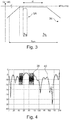
- the received input signal 5A has a frequency width Bsig, as shown in Figure 3 .
- the amplification device 4 comprises a predistortion loop 7.
- the predistortion loop 7 includes a predistortion module 8 adapted to provide a predistorded output signal 10 from the received input signal 5A, a power amplifier 14, and means 16 for filtering the predistorded output signal 10.
- the predistortion module 8 is a digital predistortion module which comprises a predistording functional block 20, a subtractor 22 and a digital predistorder 24.
- the predistortion module 8 is for example integrated within a FPGA (Field-Programmable Gate Array) or within an ASIC (Application-Specific Integrated Circuit).
- the predistording functional block 20 has a first input 26A and a second input 26B. It further has an output 28 connected to the input of the filtering means 16.
- the predistording functional block 20 is adapted to receive the input signal 5A on its first input 26A, and to provide the predistorded output signal 10 on its output 28.
- the predistorded output signal 10 is a digital signal.
- the non-inverting input of the subtractor 22 is connected to the output 28 of the predistording functional block 20.
- the output of the substractor 22 is adapted to provide a digital, time discrete error signal 29.
- the digital predistorder 24 has a first input 30A, a second input 30B, a first output 32A and a second output 32B.
- the first input 30A is connected to the output of the subtractor 22.
- the second input 30B is connected to the output of the power amplifier 14.
- the first output 32A is connected to the inverting input of the subtractor 22.
- the second output 32B is connected to the second input 26B of the predistording functional block 20.
- the digital predistorder 24 is adapted to receive, on its second input 30B, a feedback signal 34 from the output of the power amplifier 14.
- the feedback signal 34 is an analog and down-converted scaled version of the amplified output signal 5B.
- the feedback signal 34 is digitized by an analog-to-digital converter before being applied on the second input 30B, such a converter not being shown on Figure 2 for clarity reasons.
- the time discrete error signal 29 is calculated from the predistorded output signal 10 and the feedback signal 34.
- the predistortion module 8 is adapted to receive a feedback signal 34 from the output of the power amplifier 14, to determine a transmission characteristic of the power amplifier 14 from the received feedback signal 34, and to predistord the received input signal 5A according to the determined characteristic of the power amplifier 14.
- the predistortion module 8 is adapted to perform multiple iterations in order to determine the transmission characteristic of the power amplifier 14.
- the time discrete error signal 29 includes spectral portions related to the nonlinearities of the power amplifier 14. After some iterations within the predistortion loop 7, when the transmission characteristic of the power amplifier 14 have been determined, the value of the time discrete error signal 29 is almost zero and the predistording functional block 20 predistords the input signal 5A according to the determined characteristic of the power amplifier 14.
- the predistortion loop 7 forms a digital indirect learning predistortion loop. This allows to avoid distortion of the input signal 5A by the power amplifier 14, by determining the transmission characteristic of the power amplifier 14 during use of the amplification device 4, and by compensating upstream the effects of the nonlinearities of the power amplifier 14. Alternatively, the predistortion loop 7 forms a direct learning predistortion loop.
- the power amplifier 14 is adapted to provide the amplified output signal 5B.
- the power amplifier 14 comprises at least one semiconductor electronic component.
- the power amplifier 14 is an non-switched amplifier.
- the or each semiconductor electronic component is an analog radiofrequency component.
- the power amplifier 14 is a switched amplifier and the or each semiconductor electronic component is a switching electronic component.
- the or each semiconductor electronic component may be a transistor, for example a bipolar transistor or a field effect transistor.
- the or each semiconductor electronic component is an electronic field effect transistor, for example a LDMOS transistor.
- the or each electronic field effect transistor may be chosen from the non-limiting group consisting of: a VDMOS transistor, a CMOS transistor, a NMOS transistor, a PMOS transistor, a GaAs transistor and a GaN transistor.
- the power amplifier 14 further comprises at least one capacitor connected to a gate or a drain of the or one of the electronic field effect transistor(s). This feature allows to further enhance the protection of the field effect transistors by the filtering means 16, such a protection being detailed below.
- the filtering means 16 are connected between the predistortion module 8 and the power amplifier 14, and are adapted to provide a filtered signal 35 to the power amplifier 14.
- the filtering means 16 are analog filtering means and comprise an analog polynomial filter, for example a polynomial Chebyshev filter type.
- a digital-to-analog converter is arranged between the predistortion module 8 and the power amplifier 14. The digital-to-analog converter allows to convert the predistorded output signal 10 to an analog signal before it being processed by the filtering means 16.
- the filtering means 16 are digital filtering means.
- the filtering means 16 are for example integrated within the same FPGA or ASIC as that of the predistortion module 8, and a digital-to-analog converter is arranged between the filtering means 16 and the power amplifier 14.
- the filtering means 16 comprise a digital polynomial filter, for example a polynomial Chebyshev filter type.
- the filtering means 16 are configured to increase the rise time of any peak signal whose initial rise time is less than or equal to a predefined time value, and which is contained in the predistorded output signal 10, and to provide the resulting peak signal within the filtered signal 35 so as to protect the or each semiconductor electronic component.
- the or each resulting peak signal has a rise time greater than said predefined time value.
- the harmful peak signal is a spike
- the harmful peak signal has a rise time less than or equal to a predefined time value of 10 ns
- increasing the rise time of such a signal has the advantageous effect of cancelling the spike within the filtered signal 35.
- the filtering means 16 are advantageously configured to attenuate or cancel every peak signal having an initial rise time less than or equal to 10 ns, whatever its origin before the power amplifier 14 (modem, channel coding, base band, transmission part, predistortion module and so on). This allows to reduce the impact of such harmful peak signals on the power amplifier 14, while not decreasing the power capabilities of the amplification device 4 and not disturbing the amplification linearity, as will be detailed below.
- the filtering means 16 are adapted to have an enlarged bandwidth compared to an effective bandwidth ⁇ f of the radiofrequency transmitter 2.
- enlarged bandwidth it is meant in the following that the bandwidth of the filtering means 16 encompass the effective bandwidth ⁇ f of the radiofrequency transmitter 2.
- the filtering means 16 are adapted to have an upper cutoff frequency whose value is given by the sum between the value of the highest frequency of the frequency range ⁇ f of the received input signal 5A and the frequency width B sig of the input signal 5A times a numerical value.
- This numerical value is equal to 1 or 2. This allows to ensure that digital predistorder 24 gets a right image of distortion. More precisely, when the numerical value is equal to 1, as is the case in the embodiment of Figure 3 , such a design for the filtering means 16 allows not deforming the 3th order InterModulation (IMD3) component of the signal 10 predistorded by the predistortion module 8. When the numerical value is equal to 2, such a design for the filtering means 16 allows not deforming the IMD3 component and the 5th order InterModulation (IMD5) component of the predistorded signal 10.
- IMD3 3th order InterModulation
- IMD5 5th order InterModulation
- the filtering means 16 Since the filtering means 16 are included in the predistortion loop 7, the filtering means 16 must not attenuate the spectral portions related to the nonlinearities of the power amplifier 14 in the extreme cases where the received signal 5A is situated at the lowest or at the highest frequency of the effective bandwidth ⁇ f of the radiofrequency transmitter 2. In the exemplary embodiment of Figure 3 the received signal 5A is situated at the lowest frequency of the effective bandwidth ⁇ f of the radiofrequency transmitter 2.
- the filtering means 16 are adapted to have a predefined bandwidth B W19 , in particular a -19 dB bandwidth, which satisfies formula :
- B w 19 F 1 ⁇ ⁇ f + 2 ⁇ K 1 ⁇ B sig
- F 1 is a frequency value, in particular substantially equal to 200 MHz. The choice of this particular value for F1 allows to attenuate any peak signal contained in the predistorded output signal 10, whose rise time is less than or equal to 5 ns.
- K 1 is a numerical value between 1 and 3. When the numerical value K 1 is equal to 1, such a design for the filtering means 16 allows not deforming the IMD3 component of the signal 10 predistorded by the predistortion module 8. When the numerical value K 1 is equal to 3, such a design for the filtering means 16 allows not deforming the IMD3 component and the IMD5 component of the predistorded signal 10.
- the filtering means 16 are adapted to have a passband ripple whose value is more than or equal to -0.5 dB. This ensures that the amplitude variation versus frequency is in the range of digital equalization.
- the filtering means 16 are adapted to have insertion losses whose absolute value is more than or equal to -3 dB. This allows to ensure that the reserve gain for transmission is sufficient.
- the filtering means 16 are adapted to have a return loss whose absolute value is less than or equal to 10 dB. This allows to ensure that the filtering means 16 have a satisfactory adaptation to the impedance of the system.
- the filtering means 16 comprise an analog polynomial Chebyshev filter type. It is further assumed that the input signal 5A comprises several peak signals whose rise time is less than or equal to 10 ns, for example substantially equal to 5 ns. A point 36 represents each of these peak signals in the Bode diagram of Figure 3 .
- the predistording functional block 20 receives the input signal 5A on its first input 26A, and provides the predistorded output signal 10 on its output 28.
- the predistorded output signal 10 is a digital signal.
- the predistording functional block 20 predistords the input signal 5A according to the characteristic of the power amplifier 14, determined previously by the predistortion module 8 via the received feedback signal 34. Consequently, the predistorded output signal 10 comprises the spectral portions related to the nonlinearities of the power amplifier 14.
- the predistorded signal 10 is then transmitted to the filtering means 16. Thanks to their above-mentioned configuration, the filtering means 16 attenuate sufficiently each peak signal contained in the predistorded signal 10 to protect the or each semiconductor electronic component of the power amplifier 14. More precisely, the filtering means 16 increase the rise time of each peak signal contained in the predistorded signal 10, and provide within the filtered signal 35, for each initial peak signal, a resulting peak signal whose rise time is greater than 10 ns, so as to protect the or each semiconductor electronic component. This operation of the filtering means 16 is illustrated in Figures 4 to 6 .
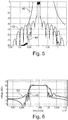
- Figure 4 is a simulated timing diagram.
- the curve 38 represents the predistorded output signal 10 over time
- the curve 40 represents the filtered signal 35 over time. It can be seen from Figure 4 that every peak signal contained in the predistorded output signal 10 has been efficiently attenuated by the filtering means 16, since the curve 40 comprises no more peak signals whose rise time is less than or equal to 10 ns. Thus, the or each semiconductor electronic component of the power amplifier 14 is efficiently protected by the filtering means 16.
- Figure 5 is a simulated frequency diagram.
- the curve 42 represents the frequency spectrum of the predistorded output signal 10, and the curve 44 represents the frequency spectrum of the filtered signal 35.
- the curve 46 represents the transfer function of the filtering means 16. From Figure 5 it can be seen how the filtering means 16 modify the frequency spectrum of the predistorded output signal 10.
- the cardinal sine portions appearing on the curve 42 are due to a particular peak signal contained in the predistorded output signal 10, which is represented in Figure 6 .
- This particular peak signal is a square signal with a strong level.
- Figure 6 is a simulated timing diagram, in which the curve 48 represents this undesired square signal over time, and the curve 50 represents the square signal over time, when filtered by the filtering means 16. From Figure 6 it can be seen that the filtering means 16 smoothen the edges of the undesired square signal so that the rise time of this signal increases up to acceptable values, i.e. to values greater than 10 ns. Thus, the or each semiconductor electronic component of the power amplifier 14 is efficiently protected by the filtering means 16.
- test bench was configured to generate many peak signals having a rise time less than or equal to 10 ns.
- the predistortion module 8, the filtering means 16 and the power amplifier 14 have been connected downstream to the test bench.
- the tests have shown that with the filtering means 16 compliant to the above-mentioned configuration, peak signals having a rise time less than or equal to 10 ns have been detected upstream of the filtering means 16, but that no such peak signal has been detected downstream of the filtering means 16.
- the characteristic and performances of the semiconductor electronic components such as gain, efficiency, linearity have been checked with success, i.e. no degradation in these parameters was detected. Tests have been repeated with different types of semiconductor electronic components and none of them broke. The same semiconductor electronic components have been tested again without the filtering means 16 and have been destroyed due to the harmful peak signals.
- the filtering means 16 comprise a stripline filter 52.
- the stripline filter 52 is a coupled line filter which has two metallic electrodes 54, for example two copper electrodes 54.
- the use of such a stripline filter for the filtering means 16 allows reducing the design time of the filtering means.
- the filtering means 16 comprise a dielectric filter 56.
- the filtering means 16 comprise a cavity filter 58.
- a cavity filter can be easily inserted within a cabinet at the output of the predistortion module 8.
- Each of these three embodiments for the filtering means 16, illustrated on Figures 7 to 9 allows providing a low volume for the filtering means. This facilitates the insertion of the filtering means within the amplification device 4, in particular when the amplification device 4 is used as a radiofrequency amplification device.
- the amplification device allows reducing the impact of harmful signals on the power amplifier so as to avoid failure of said power amplifier, while not decreasing the power capabilities of the amplification device and not disturbing the amplification linearity.
- the amplification device according to the invention has the further advantage that the filtering means can be integrated within the device either at the initial design phase of the device, or directly onsite afterwards, without requiring any additional add-on or hardware.
- any block diagrams herein represent conceptual views of illustrative circuitry embodying the principles of the invention.
- any flow charts, flow diagrams, state transition diagrams, pseudo code, and the like represent various processes which may be substantially represented in computer readable medium and so executed by a computer or processor, whether or not such computer or processor is explicitly shown.
Landscapes
- Engineering & Computer Science (AREA)
- Power Engineering (AREA)
- Physics & Mathematics (AREA)
- Nonlinear Science (AREA)
- Mathematical Analysis (AREA)
- Pure & Applied Mathematics (AREA)
- Mathematical Optimization (AREA)
- General Physics & Mathematics (AREA)
- Algebra (AREA)
- Computer Networks & Wireless Communication (AREA)
- Signal Processing (AREA)
- Microelectronics & Electronic Packaging (AREA)
- Amplifiers (AREA)
Claims (14)
- Verstärkungsvorrichtung (4), ausgelegt für die Verwendung in einem Radiofrequenzsender (2), wobei besagte Verstärkungsvorrichtung (4) umfasst eine Vorverzerrungsschleife (7), wobei besagte Vorverzerrungsschleife (7) einschließt:• ein Vorverzerrungsmodul (8), ausgelegt zum Bereitstellen eines vorverzerrten Ausgangssignals (10) aus einem empfangenen Eingangssignal (5A),• einen Leistungsverstärker (14), umfassend mindestens eine elektronische Halbleiterkomponente und• Mittel (16) zum Filtern des vorverzerrten Ausgangssignals (10), wobei besagte Mittel (16) zwischen dem Vorverzerrungsmodul (8) und dem Leistungsverstärker (14) angeschlossen sind und ausgelegt sind zum Bereitstellen eines gefilterten Signals (35) zum Leistungsverstärker (14),wobei die Filtermittel (16) konfiguriert sind zum Erhöhen der Anstiegszeit eines beliebigen Peak-Signals, dessen ursprüngliche Anstiegszeit geringer oder gleich ist einem vordefinierten Zeitwert, wobei besagtes Peak-Signal enthalten ist in dem vorverzerrten Ausgangssignal (10) und zum Bereitstellen des resultierenden Peak-Signals innerhalb des gefilterten Signals (35), um die oder jede beliebige elektronische Halbleiterkomponente zu schützen, wobei besagtes resultierendes Peak-Signal eine Anstiegszeit aufweist, die größer ist als besagter vordefinierter Zeitwert,
dadurch gekennzeichnet, dass die Filtermittel (16) ausgelegt sind, eine obere Cutoff-Frequenz aufzuweisen, deren Wert gegeben ist durch eine Summe eines Wertes der höchsten Frequenz einer effektiven Bandbreite (Δf) des Radiofrequenzsenders (2) und eines Wertes einer Frequenzbreite des Eingangssignals (5A) multipliziert mit einem numerischen Wert, wobei besagter numerischer Wert gleich 1 oder 2 ist. - Verstärkungsvorrichtung (4) nach Anspruch 1, wobei besagte mindestens eine elektronische Halbleiterkomponente eine analoge elektronische Radiofrequenzhalbleiterkomponente oder eine elektronische Radiofrequenzumschalt-Halbleiterkomponente ist.
- Verstärkungsvorrichtung (4) nach einem beliebigen der vorhergehenden Ansprüche, wobei die Filtermittel (16) ausgelegt sind, eine vordefinierte Bandbreite BW19 aufzuweisen, insbesondere eine -19 dB Bandbreite, welche die folgende Formel erfüllt:
BW19 = F1 - Δf + (2 - K1) x Bsig, wobei F1 ein Frequenzwert ist, insbesondere im Wesentlichen gleich 200 MHz, Δf die effektive Bandbreite des Radiofrequenzsenders (2) ist, K1 ein numerischer Wert zwischen 1 und 3 und Bsig die Frequenzbreite des Eingangssignals (5A). - Verstärkungsvorrichtung (4) nach einem beliebigen der vorhergehenden Ansprüche, wobei die Filtermittel (16) ausgelegt sind, eine Passbandwelligkeit aufzuweisen, deren Wert größer oder gleich -0,5 dB ist.
- Verstärkungsvorrichtung (4) nach einem beliebigen der vorhergehenden Ansprüche, wobei die Filtermittel (16) ausgelegt sind, Insertionsverluste aufzuweisen, deren Wert größer oder gleich -3 dB ist.
- Verstärkungsvorrichtung (4) nach einem beliebigen der vorhergehenden Ansprüche, wobei die Filtermittel (16) ausgelegt sind, einen Rückgabeverlust aufzuweisen, dessen Wert kleiner oder gleich 10 dB ist.
- Verstärkungsvorrichtung (4) nach einem beliebigen der vorhergehenden Ansprüche, wobei die mindestens eine elektronische Halbleiterkomponente ein bipolarer Transistor oder ein Transistor mit elektronischem Feldeffekt ist.
- Verstärkungsvorrichtung (4) nach Anspruch 7, wobei der Leistungsverstärker (14) weiterhin umfasst einen Kondensator, wobei besagter mindestens eine Kondensator mit einem Gate verbunden ist oder mit einem Drain des Transistors mit elektronischem Feldeffekt.
- Verstärkungsvorrichtung (4) nach einem beliebigen der vorhergehenden Ansprüche, wobei die Filtermittel (16) umfassen einen digitalen oder analogen Polynomfilter, zum Beispiel einen polynomiellen Filter vom Chebyshev-Typ.
- Verstärkungsvorrichtung (4) nach einem beliebigen der vorhergehenden Ansprüche, wobei die Filtermittel (16) umfassen einen Stripline-Filter (52) oder einen dielektrischen Filter (56) oder einen Hohlraumfilter (58).
- Verstärkungsvorrichtung (4) nach einem beliebigen der vorhergehenden Ansprüche, wobei das Vorzerrungsmodul (8) ausgelegt ist zum Empfangen eines Feedback-Signals (34) von einem Ausgang des Leistungsverstärkers (14) zum Bestimmen einer Sendecharakteristik des Leistungsverstärkers (14) von dem empfangenen Feedback-Signal (34) und zum Vorverzerren des Eingangssignals (5A) gemäß besagter bestimmter Sendecharakteristik des Leistungsverstärkers (14).
- Verstärkungsvorrichtung (4) nach einem beliebigen der vorhergehenden Ansprüche, wobei besagter vordefinierter Zeitwert gleich 10 ns ist.
- Radiofrequenzsender (2), umfassend eine Verstärkungsvorrichtung (4) nach einem beliebigen der vorhergehenden Ansprüche.
- Radiofrequenzsender nach Anspruch 13, wobei die Filtermittel (16) der Verstärkungsvorrichtung (4) ausgelegt sind, eine vergrößerte Bandbreite aufzuweisen im Vergleich zu einer effektiven Bandbreite des Radiofrequenzsenders, wobei besagte vergrößerte Bandbreite besagte effektive Bandbreite umfasst.
Priority Applications (1)
| Application Number | Priority Date | Filing Date | Title |
|---|---|---|---|
| EP15305580.1A EP3082257B1 (de) | 2015-04-17 | 2015-04-17 | Filter mit rückschnappschutz |
Applications Claiming Priority (1)
| Application Number | Priority Date | Filing Date | Title |
|---|---|---|---|
| EP15305580.1A EP3082257B1 (de) | 2015-04-17 | 2015-04-17 | Filter mit rückschnappschutz |
Publications (2)
| Publication Number | Publication Date |
|---|---|
| EP3082257A1 EP3082257A1 (de) | 2016-10-19 |
| EP3082257B1 true EP3082257B1 (de) | 2018-06-27 |
Family
ID=53039830
Family Applications (1)
| Application Number | Title | Priority Date | Filing Date |
|---|---|---|---|
| EP15305580.1A Not-in-force EP3082257B1 (de) | 2015-04-17 | 2015-04-17 | Filter mit rückschnappschutz |
Country Status (1)
| Country | Link |
|---|---|
| EP (1) | EP3082257B1 (de) |
Family Cites Families (2)
| Publication number | Priority date | Publication date | Assignee | Title |
|---|---|---|---|---|
| US20140146918A1 (en) * | 2012-11-27 | 2014-05-29 | Broadcom Corporation | Detection and Mitigation of an Abnormal Signal Condition Within a Power Amplifier (PA) |
| EP2959602A1 (de) * | 2013-06-13 | 2015-12-30 | Comtech EF Data Corp. | System und verfahren für verzerrungsleistungsadaptierte adaptive vorverzerrung |
-
2015
- 2015-04-17 EP EP15305580.1A patent/EP3082257B1/de not_active Not-in-force
Non-Patent Citations (1)
| Title |
|---|
| None * |
Also Published As
| Publication number | Publication date |
|---|---|
| EP3082257A1 (de) | 2016-10-19 |
Similar Documents
| Publication | Publication Date | Title |
|---|---|---|
| US9787459B2 (en) | Non-linear interference cancellation for wireless transceivers | |
| Yu et al. | Band-limited Volterra series-based digital predistortion for wideband RF power amplifiers | |
| KR102555331B1 (ko) | 전력 증폭기에 대한 전치왜곡 방법 및 그를 위한 회로 | |
| KR101845154B1 (ko) | 동적 전치 왜곡에 있어서의 적응형 파고율 감소 장치 및 방법 | |
| EP2438678B1 (de) | Vorrichtung und verfahren zur prädiktiven übersteuerungsdetektion | |
| JP4868433B2 (ja) | 歪み補償装置および歪み補償機能付き電力増幅装置 | |
| KR20120116104A (ko) | 개선된 선형적 특징을 가지는 전력 증폭기 | |
| Montoro et al. | A new digital predictive predistorter for behavioral power amplifier linearization | |
| Rudolph | GaN HEMTs for low-noise amplification—status and challenges | |
| US9214968B2 (en) | Apparatus and methods for providing a power amplifier with interference cancellation | |
| US7755425B2 (en) | Method and apparatus for reducing frequency memory effects in RF power amplifiers | |
| EP3082257B1 (de) | Filter mit rückschnappschutz | |
| Hammi et al. | Generalized twin-nonlinear two-box digital predistorter for GaN based LTE Doherty power amplifiers with strong memory effects | |
| EP3255791B1 (de) | Stromverstärkungsausrüstung | |
| Manyam et al. | An FIR memory polynomial predistorter for wideband RF power amplifiers | |
| KR101093644B1 (ko) | 음의 군지연 회로를 갖는 아날로그 피드백 선형 전력 증폭기 | |
| KR102863361B1 (ko) | 전력 증폭기의 전하 트래핑 효과들을 위해 전송 신호를 보상하는 시스템들 및 방법들 | |
| KR100819307B1 (ko) | 델타-시그마 변조된 신호를 사용하는 전력 증폭기의 입력정합 장치 및 방법 | |
| JP2014096794A (ja) | 瞬時電力制限機能を備えたrfチャネル増幅モジュール | |
| US8427234B1 (en) | Method and apparatus for predistorting a signal | |
| KR100964335B1 (ko) | 전력증폭기의 디지털 전치왜곡 보상방법 | |
| Peng et al. | Digital harmonic canceling algorithm for power amplifiers based on nonlinear adaptive filter | |
| Hamoud et al. | Evaluation of an optimal digital predistorter for multistandard systems | |
| Panigrahi et al. | A Novel Software-Defined Radio Transceiver System with a Dynamic and Adaptive Digital Pre-distortion Solution | |
| EP4618412A1 (de) | Mehrstufiger lastmodulierter symmetrischer verstärker |
Legal Events
| Date | Code | Title | Description |
|---|---|---|---|
| PUAI | Public reference made under article 153(3) epc to a published international application that has entered the european phase |
Free format text: ORIGINAL CODE: 0009012 |
|
| AK | Designated contracting states |
Kind code of ref document: A1 Designated state(s): AL AT BE BG CH CY CZ DE DK EE ES FI FR GB GR HR HU IE IS IT LI LT LU LV MC MK MT NL NO PL PT RO RS SE SI SK SM TR |
|
| AX | Request for extension of the european patent |
Extension state: BA ME |
|
| STAA | Information on the status of an ep patent application or granted ep patent |
Free format text: STATUS: REQUEST FOR EXAMINATION WAS MADE |
|
| 17P | Request for examination filed |
Effective date: 20161128 |
|
| RBV | Designated contracting states (corrected) |
Designated state(s): AL AT BE BG CH CY CZ DE DK EE ES FI FR GB GR HR HU IE IS IT LI LT LU LV MC MK MT NL NO PL PT RO RS SE SI SK SM TR |
|
| STAA | Information on the status of an ep patent application or granted ep patent |
Free format text: STATUS: EXAMINATION IS IN PROGRESS |
|
| 17Q | First examination report despatched |
Effective date: 20170118 |
|
| RAP1 | Party data changed (applicant data changed or rights of an application transferred) |
Owner name: ALCATEL LUCENT |
|
| GRAP | Despatch of communication of intention to grant a patent |
Free format text: ORIGINAL CODE: EPIDOSNIGR1 |
|
| STAA | Information on the status of an ep patent application or granted ep patent |
Free format text: STATUS: GRANT OF PATENT IS INTENDED |
|
| GRAS | Grant fee paid |
Free format text: ORIGINAL CODE: EPIDOSNIGR3 |
|
| INTG | Intention to grant announced |
Effective date: 20180423 |
|
| GRAA | (expected) grant |
Free format text: ORIGINAL CODE: 0009210 |
|
| STAA | Information on the status of an ep patent application or granted ep patent |
Free format text: STATUS: THE PATENT HAS BEEN GRANTED |
|
| AK | Designated contracting states |
Kind code of ref document: B1 Designated state(s): AL AT BE BG CH CY CZ DE DK EE ES FI FR GB GR HR HU IE IS IT LI LT LU LV MC MK MT NL NO PL PT RO RS SE SI SK SM TR |
|
| REG | Reference to a national code |
Ref country code: GB Ref legal event code: FG4D |
|
| REG | Reference to a national code |
Ref country code: AT Ref legal event code: REF Ref document number: 1013203 Country of ref document: AT Kind code of ref document: T Effective date: 20180715 |
|
| REG | Reference to a national code |
Ref country code: IE Ref legal event code: FG4D |
|
| REG | Reference to a national code |
Ref country code: DE Ref legal event code: R096 Ref document number: 602015012697 Country of ref document: DE |
|
| PG25 | Lapsed in a contracting state [announced via postgrant information from national office to epo] |
Ref country code: SE Free format text: LAPSE BECAUSE OF FAILURE TO SUBMIT A TRANSLATION OF THE DESCRIPTION OR TO PAY THE FEE WITHIN THE PRESCRIBED TIME-LIMIT Effective date: 20180627 Ref country code: NO Free format text: LAPSE BECAUSE OF FAILURE TO SUBMIT A TRANSLATION OF THE DESCRIPTION OR TO PAY THE FEE WITHIN THE PRESCRIBED TIME-LIMIT Effective date: 20180927 Ref country code: LT Free format text: LAPSE BECAUSE OF FAILURE TO SUBMIT A TRANSLATION OF THE DESCRIPTION OR TO PAY THE FEE WITHIN THE PRESCRIBED TIME-LIMIT Effective date: 20180627 Ref country code: FI Free format text: LAPSE BECAUSE OF FAILURE TO SUBMIT A TRANSLATION OF THE DESCRIPTION OR TO PAY THE FEE WITHIN THE PRESCRIBED TIME-LIMIT Effective date: 20180627 Ref country code: BG Free format text: LAPSE BECAUSE OF FAILURE TO SUBMIT A TRANSLATION OF THE DESCRIPTION OR TO PAY THE FEE WITHIN THE PRESCRIBED TIME-LIMIT Effective date: 20180927 |
|
| REG | Reference to a national code |
Ref country code: NL Ref legal event code: MP Effective date: 20180627 |
|
| REG | Reference to a national code |
Ref country code: LT Ref legal event code: MG4D |
|
| PG25 | Lapsed in a contracting state [announced via postgrant information from national office to epo] |
Ref country code: GR Free format text: LAPSE BECAUSE OF FAILURE TO SUBMIT A TRANSLATION OF THE DESCRIPTION OR TO PAY THE FEE WITHIN THE PRESCRIBED TIME-LIMIT Effective date: 20180928 Ref country code: RS Free format text: LAPSE BECAUSE OF FAILURE TO SUBMIT A TRANSLATION OF THE DESCRIPTION OR TO PAY THE FEE WITHIN THE PRESCRIBED TIME-LIMIT Effective date: 20180627 Ref country code: HR Free format text: LAPSE BECAUSE OF FAILURE TO SUBMIT A TRANSLATION OF THE DESCRIPTION OR TO PAY THE FEE WITHIN THE PRESCRIBED TIME-LIMIT Effective date: 20180627 Ref country code: LV Free format text: LAPSE BECAUSE OF FAILURE TO SUBMIT A TRANSLATION OF THE DESCRIPTION OR TO PAY THE FEE WITHIN THE PRESCRIBED TIME-LIMIT Effective date: 20180627 |
|
| REG | Reference to a national code |
Ref country code: AT Ref legal event code: MK05 Ref document number: 1013203 Country of ref document: AT Kind code of ref document: T Effective date: 20180627 |
|
| PG25 | Lapsed in a contracting state [announced via postgrant information from national office to epo] |
Ref country code: NL Free format text: LAPSE BECAUSE OF FAILURE TO SUBMIT A TRANSLATION OF THE DESCRIPTION OR TO PAY THE FEE WITHIN THE PRESCRIBED TIME-LIMIT Effective date: 20180627 |
|
| PG25 | Lapsed in a contracting state [announced via postgrant information from national office to epo] |
Ref country code: SK Free format text: LAPSE BECAUSE OF FAILURE TO SUBMIT A TRANSLATION OF THE DESCRIPTION OR TO PAY THE FEE WITHIN THE PRESCRIBED TIME-LIMIT Effective date: 20180627 Ref country code: CZ Free format text: LAPSE BECAUSE OF FAILURE TO SUBMIT A TRANSLATION OF THE DESCRIPTION OR TO PAY THE FEE WITHIN THE PRESCRIBED TIME-LIMIT Effective date: 20180627 Ref country code: RO Free format text: LAPSE BECAUSE OF FAILURE TO SUBMIT A TRANSLATION OF THE DESCRIPTION OR TO PAY THE FEE WITHIN THE PRESCRIBED TIME-LIMIT Effective date: 20180627 Ref country code: EE Free format text: LAPSE BECAUSE OF FAILURE TO SUBMIT A TRANSLATION OF THE DESCRIPTION OR TO PAY THE FEE WITHIN THE PRESCRIBED TIME-LIMIT Effective date: 20180627 Ref country code: IS Free format text: LAPSE BECAUSE OF FAILURE TO SUBMIT A TRANSLATION OF THE DESCRIPTION OR TO PAY THE FEE WITHIN THE PRESCRIBED TIME-LIMIT Effective date: 20181027 Ref country code: AT Free format text: LAPSE BECAUSE OF FAILURE TO SUBMIT A TRANSLATION OF THE DESCRIPTION OR TO PAY THE FEE WITHIN THE PRESCRIBED TIME-LIMIT Effective date: 20180627 Ref country code: PL Free format text: LAPSE BECAUSE OF FAILURE TO SUBMIT A TRANSLATION OF THE DESCRIPTION OR TO PAY THE FEE WITHIN THE PRESCRIBED TIME-LIMIT Effective date: 20180627 |
|
| PG25 | Lapsed in a contracting state [announced via postgrant information from national office to epo] |
Ref country code: IT Free format text: LAPSE BECAUSE OF FAILURE TO SUBMIT A TRANSLATION OF THE DESCRIPTION OR TO PAY THE FEE WITHIN THE PRESCRIBED TIME-LIMIT Effective date: 20180627 Ref country code: SM Free format text: LAPSE BECAUSE OF FAILURE TO SUBMIT A TRANSLATION OF THE DESCRIPTION OR TO PAY THE FEE WITHIN THE PRESCRIBED TIME-LIMIT Effective date: 20180627 Ref country code: ES Free format text: LAPSE BECAUSE OF FAILURE TO SUBMIT A TRANSLATION OF THE DESCRIPTION OR TO PAY THE FEE WITHIN THE PRESCRIBED TIME-LIMIT Effective date: 20180627 |
|
| REG | Reference to a national code |
Ref country code: DE Ref legal event code: R097 Ref document number: 602015012697 Country of ref document: DE |
|
| PLBE | No opposition filed within time limit |
Free format text: ORIGINAL CODE: 0009261 |
|
| STAA | Information on the status of an ep patent application or granted ep patent |
Free format text: STATUS: NO OPPOSITION FILED WITHIN TIME LIMIT |
|
| PG25 | Lapsed in a contracting state [announced via postgrant information from national office to epo] |
Ref country code: DK Free format text: LAPSE BECAUSE OF FAILURE TO SUBMIT A TRANSLATION OF THE DESCRIPTION OR TO PAY THE FEE WITHIN THE PRESCRIBED TIME-LIMIT Effective date: 20180627 |
|
| 26N | No opposition filed |
Effective date: 20190328 |
|
| PG25 | Lapsed in a contracting state [announced via postgrant information from national office to epo] |
Ref country code: SI Free format text: LAPSE BECAUSE OF FAILURE TO SUBMIT A TRANSLATION OF THE DESCRIPTION OR TO PAY THE FEE WITHIN THE PRESCRIBED TIME-LIMIT Effective date: 20180627 |
|
| REG | Reference to a national code |
Ref country code: DE Ref legal event code: R119 Ref document number: 602015012697 Country of ref document: DE |
|
| PG25 | Lapsed in a contracting state [announced via postgrant information from national office to epo] |
Ref country code: AL Free format text: LAPSE BECAUSE OF FAILURE TO SUBMIT A TRANSLATION OF THE DESCRIPTION OR TO PAY THE FEE WITHIN THE PRESCRIBED TIME-LIMIT Effective date: 20180627 |
|
| REG | Reference to a national code |
Ref country code: CH Ref legal event code: PL |
|
| REG | Reference to a national code |
Ref country code: BE Ref legal event code: MM Effective date: 20190430 |
|
| GBPC | Gb: european patent ceased through non-payment of renewal fee |
Effective date: 20190417 |
|
| PG25 | Lapsed in a contracting state [announced via postgrant information from national office to epo] |
Ref country code: LU Free format text: LAPSE BECAUSE OF NON-PAYMENT OF DUE FEES Effective date: 20190417 Ref country code: MC Free format text: LAPSE BECAUSE OF FAILURE TO SUBMIT A TRANSLATION OF THE DESCRIPTION OR TO PAY THE FEE WITHIN THE PRESCRIBED TIME-LIMIT Effective date: 20180627 |
|
| PG25 | Lapsed in a contracting state [announced via postgrant information from national office to epo] |
Ref country code: DE Free format text: LAPSE BECAUSE OF NON-PAYMENT OF DUE FEES Effective date: 20191101 Ref country code: LI Free format text: LAPSE BECAUSE OF NON-PAYMENT OF DUE FEES Effective date: 20190430 Ref country code: CH Free format text: LAPSE BECAUSE OF NON-PAYMENT OF DUE FEES Effective date: 20190430 Ref country code: GB Free format text: LAPSE BECAUSE OF NON-PAYMENT OF DUE FEES Effective date: 20190417 |
|
| PG25 | Lapsed in a contracting state [announced via postgrant information from national office to epo] |
Ref country code: BE Free format text: LAPSE BECAUSE OF NON-PAYMENT OF DUE FEES Effective date: 20190430 Ref country code: FR Free format text: LAPSE BECAUSE OF NON-PAYMENT OF DUE FEES Effective date: 20190430 |
|
| PG25 | Lapsed in a contracting state [announced via postgrant information from national office to epo] |
Ref country code: TR Free format text: LAPSE BECAUSE OF FAILURE TO SUBMIT A TRANSLATION OF THE DESCRIPTION OR TO PAY THE FEE WITHIN THE PRESCRIBED TIME-LIMIT Effective date: 20180627 |
|
| PG25 | Lapsed in a contracting state [announced via postgrant information from national office to epo] |
Ref country code: IE Free format text: LAPSE BECAUSE OF NON-PAYMENT OF DUE FEES Effective date: 20190417 |
|
| PG25 | Lapsed in a contracting state [announced via postgrant information from national office to epo] |
Ref country code: PT Free format text: LAPSE BECAUSE OF FAILURE TO SUBMIT A TRANSLATION OF THE DESCRIPTION OR TO PAY THE FEE WITHIN THE PRESCRIBED TIME-LIMIT Effective date: 20181029 |
|
| PG25 | Lapsed in a contracting state [announced via postgrant information from national office to epo] |
Ref country code: CY Free format text: LAPSE BECAUSE OF FAILURE TO SUBMIT A TRANSLATION OF THE DESCRIPTION OR TO PAY THE FEE WITHIN THE PRESCRIBED TIME-LIMIT Effective date: 20180627 |
|
| PG25 | Lapsed in a contracting state [announced via postgrant information from national office to epo] |
Ref country code: HU Free format text: LAPSE BECAUSE OF FAILURE TO SUBMIT A TRANSLATION OF THE DESCRIPTION OR TO PAY THE FEE WITHIN THE PRESCRIBED TIME-LIMIT; INVALID AB INITIO Effective date: 20150417 Ref country code: MT Free format text: LAPSE BECAUSE OF FAILURE TO SUBMIT A TRANSLATION OF THE DESCRIPTION OR TO PAY THE FEE WITHIN THE PRESCRIBED TIME-LIMIT Effective date: 20180627 |
|
| PG25 | Lapsed in a contracting state [announced via postgrant information from national office to epo] |
Ref country code: MK Free format text: LAPSE BECAUSE OF FAILURE TO SUBMIT A TRANSLATION OF THE DESCRIPTION OR TO PAY THE FEE WITHIN THE PRESCRIBED TIME-LIMIT Effective date: 20180627 |