EP3084525B1 - Appareil lithographique et méthode de fabrication d'un dispositif - Google Patents
Appareil lithographique et méthode de fabrication d'un dispositif Download PDFInfo
- Publication number
- EP3084525B1 EP3084525B1 EP14802416.9A EP14802416A EP3084525B1 EP 3084525 B1 EP3084525 B1 EP 3084525B1 EP 14802416 A EP14802416 A EP 14802416A EP 3084525 B1 EP3084525 B1 EP 3084525B1
- Authority
- EP
- European Patent Office
- Prior art keywords
- signal
- stage
- drive signal
- control device
- drive
- Prior art date
- Legal status (The legal status is an assumption and is not a legal conclusion. Google has not performed a legal analysis and makes no representation as to the accuracy of the status listed.)
- Active
Links
Images


Classifications
-
- G—PHYSICS
- G03—PHOTOGRAPHY; CINEMATOGRAPHY; ANALOGOUS TECHNIQUES USING WAVES OTHER THAN OPTICAL WAVES; ELECTROGRAPHY; HOLOGRAPHY
- G03F—PHOTOMECHANICAL PRODUCTION OF TEXTURED OR PATTERNED SURFACES, e.g. FOR PRINTING, FOR PROCESSING OF SEMICONDUCTOR DEVICES; MATERIALS THEREFOR; ORIGINALS THEREFOR; APPARATUS SPECIALLY ADAPTED THEREFOR
- G03F7/00—Photomechanical, e.g. photolithographic, production of textured or patterned surfaces, e.g. printing surfaces; Materials therefor, e.g. comprising photoresists; Apparatus specially adapted therefor
- G03F7/70—Microphotolithographic exposure; Apparatus therefor
- G03F7/70691—Handling of masks or workpieces
- G03F7/70716—Stages
- G03F7/70725—Stages control
-
- G—PHYSICS
- G03—PHOTOGRAPHY; CINEMATOGRAPHY; ANALOGOUS TECHNIQUES USING WAVES OTHER THAN OPTICAL WAVES; ELECTROGRAPHY; HOLOGRAPHY
- G03F—PHOTOMECHANICAL PRODUCTION OF TEXTURED OR PATTERNED SURFACES, e.g. FOR PRINTING, FOR PROCESSING OF SEMICONDUCTOR DEVICES; MATERIALS THEREFOR; ORIGINALS THEREFOR; APPARATUS SPECIALLY ADAPTED THEREFOR
- G03F7/00—Photomechanical, e.g. photolithographic, production of textured or patterned surfaces, e.g. printing surfaces; Materials therefor, e.g. comprising photoresists; Apparatus specially adapted therefor
- G03F7/70—Microphotolithographic exposure; Apparatus therefor
- G03F7/70483—Information management; Active and passive control; Testing; Wafer monitoring, e.g. pattern monitoring
- G03F7/70591—Testing optical components
- G03F7/706—Aberration measurement
-
- G—PHYSICS
- G03—PHOTOGRAPHY; CINEMATOGRAPHY; ANALOGOUS TECHNIQUES USING WAVES OTHER THAN OPTICAL WAVES; ELECTROGRAPHY; HOLOGRAPHY
- G03F—PHOTOMECHANICAL PRODUCTION OF TEXTURED OR PATTERNED SURFACES, e.g. FOR PRINTING, FOR PROCESSING OF SEMICONDUCTOR DEVICES; MATERIALS THEREFOR; ORIGINALS THEREFOR; APPARATUS SPECIALLY ADAPTED THEREFOR
- G03F7/00—Photomechanical, e.g. photolithographic, production of textured or patterned surfaces, e.g. printing surfaces; Materials therefor, e.g. comprising photoresists; Apparatus specially adapted therefor
- G03F7/70—Microphotolithographic exposure; Apparatus therefor
- G03F7/70691—Handling of masks or workpieces
- G03F7/70716—Stages
-
- G—PHYSICS
- G03—PHOTOGRAPHY; CINEMATOGRAPHY; ANALOGOUS TECHNIQUES USING WAVES OTHER THAN OPTICAL WAVES; ELECTROGRAPHY; HOLOGRAPHY
- G03F—PHOTOMECHANICAL PRODUCTION OF TEXTURED OR PATTERNED SURFACES, e.g. FOR PRINTING, FOR PROCESSING OF SEMICONDUCTOR DEVICES; MATERIALS THEREFOR; ORIGINALS THEREFOR; APPARATUS SPECIALLY ADAPTED THEREFOR
- G03F7/00—Photomechanical, e.g. photolithographic, production of textured or patterned surfaces, e.g. printing surfaces; Materials therefor, e.g. comprising photoresists; Apparatus specially adapted therefor
- G03F7/70—Microphotolithographic exposure; Apparatus therefor
- G03F7/70691—Handling of masks or workpieces
- G03F7/70775—Position control, e.g. interferometers or encoders for determining the stage position
-
- G—PHYSICS
- G03—PHOTOGRAPHY; CINEMATOGRAPHY; ANALOGOUS TECHNIQUES USING WAVES OTHER THAN OPTICAL WAVES; ELECTROGRAPHY; HOLOGRAPHY
- G03F—PHOTOMECHANICAL PRODUCTION OF TEXTURED OR PATTERNED SURFACES, e.g. FOR PRINTING, FOR PROCESSING OF SEMICONDUCTOR DEVICES; MATERIALS THEREFOR; ORIGINALS THEREFOR; APPARATUS SPECIALLY ADAPTED THEREFOR
- G03F9/00—Registration or positioning of originals, masks, frames, photographic sheets or textured or patterned surfaces, e.g. automatically
- G03F9/70—Registration or positioning of originals, masks, frames, photographic sheets or textured or patterned surfaces, e.g. automatically for microlithography
- G03F9/7092—Signal processing
Definitions
- the present invention relates to a control device for controlling a synchronous positioning of a multi-body system, a lithographic apparatus and a method for manufacturing a device.
- a lithographic apparatus is a machine that applies a desired pattern onto a substrate, usually onto a target portion of the substrate.
- a lithographic apparatus can be used, for example, in the manufacture of integrated circuits (ICs).
- a patterning device which is alternatively referred to as a mask or a reticle, may be used to generate a circuit pattern to be formed on an individual layer of the IC.
- This pattern can be transferred onto a target portion (e.g. including part of, one, or several dies) on a substrate (e.g. a silicon wafer). Transfer of the pattern is typically via imaging onto a layer of radiation-sensitive material (resist) provided on the substrate.
- resist radiation-sensitive material
- a single substrate will contain a network of adjacent target portions that are successively patterned.
- Conventional lithographic apparatus include so-called steppers, in which each target portion is irradiated by exposing an entire pattern onto the target portion at once, and so-called scanners, in which each target portion is irradiated by scanning the pattern through a radiation beam in a given direction (the "scanning"-direction) while synchronously scanning the substrate parallel or anti-parallel to this direction.
- a relative position between the target portion and the pattern should be in accordance with a desired position or set point, thus ensuring that the pattern is projected on the appropriate position on the substrate.
- the position of the substrate (comprising the target portion) and the patterning device is controlled by controlling the position of the supports (or stages) to which the substrate and patterning device are mounted.
- a pair of separate closed loop controllers is applied for both controlling a set point to be followed by the stage provided with the patterning device (or reticle) and a set point to be followed by the stage provided with a substrate.
- both stages are independently controlled to each follow a particular set point, which set point is configured in such manner that the desired synchronous operation is achieved.
- a more advanced control strategy as e.g.
- a position error of the substrate stage i.e. the stage provided with the substrate
- a control signal for controlling a position of the reticle stage i.e. the stage provided with the reticle
- such approach is referred to as a feedthrough method, whereby a position error of the substrate stage is fed through to the controller of the reticle stage.
- a control device for controlling a synchronous positioning of a multi-body system comprising:
- a control method for controlling a synchronous operation of a multi-body system comprising the steps of:
- FIG. 1 schematically depicts a lithographic apparatus according to one embodiment of the invention.
- the apparatus includes an illumination system (illuminator) IL configured to condition a radiation beam B (e.g. UV radiation or any other suitable radiation), a mask support structure (e.g. a mask table) MT constructed to support a patterning device (e.g. a mask) MA and connected to a first positioning device PM configured to accurately position the patterning device in accordance with certain parameters.
- the apparatus also includes a substrate table (e.g. a wafer table) WT or "substrate support" constructed to hold a substrate (e.g. a resist-coated wafer) W and connected to a second positioning device PW configured to accurately position the substrate in accordance with certain parameters.
- a radiation beam B e.g. UV radiation or any other suitable radiation
- a mask support structure e.g. a mask table
- MT constructed to support a patterning device (e.g. a mask) MA and connected to a
- the apparatus further includes a projection system (e.g. a refractive projection lens system) PS configured to project a pattern imparted to the radiation beam B by patterning device MA onto a target portion C (e.g. including one or more dies) of the substrate W.
- a projection system e.g. a refractive projection lens system
- PS configured to project a pattern imparted to the radiation beam B by patterning device MA onto a target portion C (e.g. including one or more dies) of the substrate W.
- the illumination system may include various types of optical components, such as refractive, reflective, magnetic, electromagnetic, electrostatic or other types of optical components, or any combination thereof, for directing, shaping, or controlling radiation.
- optical components such as refractive, reflective, magnetic, electromagnetic, electrostatic or other types of optical components, or any combination thereof, for directing, shaping, or controlling radiation.
- the mask support structure supports, i.e. bears the weight of, the patterning device. It holds the patterning device in a manner that depends on the orientation of the patterning device, the design of the lithographic apparatus, and other conditions, such as for example whether or not the patterning device is held in a vacuum environment.
- the mask support structure can use mechanical, vacuum, electrostatic or other clamping techniques to hold the patterning device.
- the mask support structure may be a frame or a table, for example, which may be fixed or movable as required.
- the mask support structure may ensure that the patterning device is at a desired position, for example with respect to the projection system. Any use of the terms "reticle” or “mask” herein may be considered synonymous with the more general term "patterning device.”
- patterning device used herein should be broadly interpreted as referring to any device that can be used to impart a radiation beam with a pattern in its cross-section so as to create a pattern in a target portion of the substrate. It should be noted that the pattern imparted to the radiation beam may not exactly correspond to the desired pattern in the target portion of the substrate, for example if the pattern includes phase-shifting features or so called assist features. Generally, the pattern imparted to the radiation beam will correspond to a particular functional layer in a device being created in the target portion, such as an integrated circuit.
- the patterning device may be transmissive or reflective.
- Examples of patterning devices include masks, programmable mirror arrays, and programmable LCD panels.
- Masks are well known in lithography, and include mask types such as binary, alternating phase-shift, and attenuated phase-shift, as well as various hybrid mask types.
- An example of a programmable mirror array employs a matrix arrangement of small mirrors, each of which can be individually tilted so as to reflect an incoming radiation beam in different directions. The tilted mirrors impart a pattern in a radiation beam which is reflected by the mirror matrix.
- projection system used herein should be broadly interpreted as encompassing any type of projection system, including refractive, reflective, catadioptric, magnetic, electromagnetic and electrostatic optical systems, or any combination thereof, as appropriate for the exposure radiation being used, or for other factors such as the use of an immersion liquid or the use of a vacuum. Any use of the term “projection lens” herein may be considered as synonymous with the more general term “projection system”.
- the apparatus is of a transmissive type (e.g. employing a transmissive mask).
- the apparatus may be of a reflective type (e.g. employing a programmable mirror array of a type as referred to above, or employing a reflective mask).
- the lithographic apparatus may be of a type having two (dual stage) or more substrate tables or “substrate supports” (and/or two or more mask tables or “mask supports”).
- substrate tables or “substrate supports” and/or two or more mask tables or “mask supports”
- additional tables or supports may be used in parallel, or preparatory steps may be carried out on one or more tables or supports while one or more other tables or supports are being used for exposure.
- the lithographic apparatus may also be of a type wherein at least a portion of the substrate may be covered by a liquid having a relatively high refractive index, e.g. water, so as to fill a space between the projection system and the substrate.
- a liquid having a relatively high refractive index e.g. water
- An immersion liquid may also be applied to other spaces in the lithographic apparatus, for example, between the mask and the projection system. Immersion techniques can be used to increase the numerical aperture of projection systems.
- immersion as used herein does not mean that a structure, such as a substrate, must be submerged in liquid, but rather only means that a liquid is located between the projection system and the substrate during exposure.
- the illuminator IL receives a radiation beam from a radiation source SO.
- the source and the lithographic apparatus may be separate entities, for example when the source is an excimer laser. In such cases, the source is not considered to form part of the lithographic apparatus and the radiation beam is passed from the source SO to the illuminator IL with the aid of a beam delivery system BD including, for example, suitable directing mirrors and/or a beam expander. In other cases the source may be an integral part of the lithographic apparatus, for example when the source is a mercury lamp.
- the source SO and the illuminator IL, together with the beam delivery system BD if required, may be referred to as a radiation system.
- the illuminator IL may include an adjuster AD configured to adjust the angular intensity distribution of the radiation beam. Generally, at least the outer and/or inner radial extent (commonly referred to as ⁇ -outer and ⁇ -inner, respectively) of the intensity distribution in a pupil plane of the illuminator can be adjusted.
- the illuminator IL may include various other components, such as an integrator IN and a condenser CO. The illuminator may be used to condition the radiation beam, to have a desired uniformity and intensity distribution in its cross-section.
- the radiation beam B is incident on the patterning device (e.g., mask MA), which is held on the mask support structure (e.g., mask table MT), and is patterned by the patterning device. Having traversed the mask MA, the radiation beam B passes through the projection system PS, which focuses the beam onto a target portion C of the substrate W.
- the substrate table WT can be moved accurately, e.g. so as to position different target portions C in the path of the radiation beam B.
- the first positioning device PM and another position sensor can be used to accurately position the mask MA with respect to the path of the radiation beam B, e.g. after mechanical retrieval from a mask library, or during a scan.
- movement of the mask table MT may be realized with the aid of a long-stroke module (coarse positioning) and a short-stroke module (fine positioning), which form part of the first positioning device PM.
- movement of the substrate table WT or "substrate support" may be realized using a long-stroke module and a short-stroke module, which form part of the second positioner PW.
- the lithographic apparatus further comprises a control device CU according to the present invention for controlling the synchronous displacement and positioning of at least the mask stage (provided with the mask table MT) and the substrate stage (provided with the substrate table WT).
- the control device CU may however be configured to control a displacement or positioning of other parts or movable bodies of the apparatus as well.
- Other movable bodies in a lithographic apparatus may e.g. include optical components or devices such as lenses or mirrors or reticle masking blades.
- 'stage' may also be used to refer to a positioner or positioning device configured to position sensors or optical components (such as mirrors or lenses or masking blades).
- a control device may be applied to control those stages as well.
- the mask table MT may be connected to a short-stroke actuator only, or may be fixed.
- Mask MA and substrate W may be aligned using mask alignment marks M1, M2 and substrate alignment marks PI, P2.
- the substrate alignment marks as illustrated occupy dedicated target portions, they may be located in spaces between target portions (these are known as scribe-lane alignment marks).
- the mask alignment marks may be located between the dies.
- the depicted apparatus could be used in at least one of the following modes:
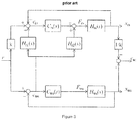
- Figure 2 schematically shows a control scheme as applied in a known lithographical apparatus for controlling a synchronous displacement of a reticle stage (or mask stage) and a wafer stage (or substrate stage).
- r represents a desired trajectory or set point to be followed by a wafer stage (subscript ws).
- the reticle stage (subscript rs) needs to follow the trajectory r multiplied by a factor k (typically 4 or 5) to take a magnification of the projection system of the apparatus into account.
- the control scheme further shows a first controller C rs (s) for determining a drive signal F rs based on an error signal e rs , the error signal e rs representing a difference between the desired position of the reticle stage and an actual measured position x rs of the reticle stage and a second controller C ws (s) for determining a drive signal F ws based on an error signal e ws , the error signal e ws representing a difference between the desired position of the wafer stage and an actual measured position x ws of the wafer stage.
- H rs (s) and H ws (s) schematically represent a conversion of a respective driving force F rs and F ws to an actual position x rs and x ws of the reticle stage and the wafer stage.
- H rs (s) and H ws (s) may thus be considered as the mechanical transfer functions of the reticle stage and the wafer stage.
- Figure 2 further shows the determination of a position error e wr between the reticle stage and the wafer stage, based on the actual positions x rs and x ws of the reticle stage and the wafer stage.
- both controllers C rs (s) and C ws (s) operate independent of each other, each determining a driving force (F rs / F ws ) to reduce the position error of the respective stage.
- FIG 3 another control scheme as applied in a known lithographical apparatus is schematically shown. The same symbols are used as in Figure 2 .
- the control scheme of Figure 3 further includes a so-called feedthrough path of the wafer stage position error to the reticle stage controller.
- the wafer stage error e ws is provided both as an input to controller C rs (s), via transfer function H r1 (s), and as an additional driving force for controlling the reticle stage (represented by the transfer function H rs (s)), via transfer function H r2 (s).
- H r2 (s) thus converts the wafer stage error e ws to an additional driving force.
- the control scheme of Figure 3 may advantageously be applied in case the response speed of the reticle stage is faster than that of the wafer stage. In such situation, feeding the wafer stage error to the reticle stage (i.e. the stage having the faster response), helps in reducing the error e wr which represents the position error between the reticle stage and the wafer stage, said error directly affecting the quality of the exposure process, i.e. the process whereby a pattern provided on a reticle that is mounted on the reticle stage is projected onto a target portion of a wafer that is mounted on the wafer stage.
- the inventors of the present invention have devised a further improvement to the method as described in US 6,373,072 , whereby the present invention may be applied irrespective of whether there is a difference in the response speed or responsiveness between the stages or not.
- the wafer stage may have a lower eigenfrequency than a reticle stage.
- a less aggressive control scheme needs to be adopted, resulting in a wafer stage being slower in responding to a disturbance or desired positioning.
- Figure 4 schematically shows a first embodiment of a control device CU according to the present invention.
- Figure 4 schematically shows a control scheme as can be applied to control a reticle stage and a wafer stage in a lithographic apparatus. It should be noted however that the control device CU as shown may also be applied to control a synchronous movement of other types of stages, in general, of other moving objects or bodies.
- a set point or trajectory r represents a desired position of the wafer stage, whereas k times r represents a desired position of the reticle stage.
- a predetermined relationship may exists between a desired position (or set point) of a first object or body and a desired position (or set point) of a second object or body.
- the control device CU is configured to receive, e.g.
- the control device CU comprises, similar to the arrangement shown in Figure 2 , a first controller C rs (s) for determining a primary drive signal (F r1 ) based on the error signal e rs and a second controller C ws (s) for determining a primary drive signal (F w1 ) based on the error signal e ws .
- the controllers C rs (s) and C ws (s) may e.g. comprise a PID controller or the like.
- a secondary drive signal is further provided for both stages.
- the control device CU is configured to determine a secondary drive signal F r2 for the reticle stage based on the error signal e ws of the wafer stage and a secondary drive signal F w2 for the wafer stage based on the error signal e rs of the reticle stage.
- the primary and secondary drive signals are combined to obtain combined drive signals F rc and F wc for respectively driving the reticle stage (represented by the mechanical transfer function H rs (s)) and the wafer stage (represented by the mechanical transfer function H ws (s)).
- the mechanical transfer functions represent a conversion from a drive signal or force to an actual position or displacement; i.e. they represent the actual behavior of the system H representing the wafer and reticle stage when a force (F rc or F wc ) are applied.
- the transfer functions as applied in the feedthrough paths i.e.
- the feedthrough of the wafer stage error e ws and the reticle stage error e rs represent a conversion which is an inverse conversion as provided by the mechanical transfer functions; i.e. they represent a conversion from a position or displacement to a force (i.e. the secondary drive signals and F r2 and F w2 ).
- these functions could be derived therefrom.
- H r2 (s) 1/H rs (s)
- the secondary drive signal F r2 would correspond to the required reticle stage input to compensate for the wafer stage error e ws .
- H w2 (s) 1/H ws (s)
- the secondary drive signal F w2 would correspond to the required wafer stage input to compensate for the reticle stage error e rs .
- the transfer function H r2 (s) preferably includes a low-pass filter (LPF), e.g. a low pass filter having a -4 or -2 gain.
- the transfer function H w2 (s) preferably also includes a low-pass filter (LPF) such as a low pass filter having a -4 or -2 gain.
- the controller input signal associated with the first stage is provided as input to the controller of the second stage and vice versa.
- Such an embodiment is schematically shown in Figure 5 .
- the error signal e ws is fed through via transfer function H r1 (s) to the input of the reticle stage controller C rs (s).
- the error signal e rs is fed through via transfer function H w1 (s) to the input of the wafer stage controller C ws (s). Because this feedthrough is applied for both stages, an additional feedback loop has been created.
- the wafer stage controller C ws (s) now encounters a transfer function that is partly defined by the reticle stage closed loop.
- the reticle stage controller C rs (s) now encounters a transfer function that is partly defined by the wafer stage closed loop.
- the reticle stage controller receives, as an input, a signal u r that is a function of H w1 . Similar observations can be made regarding the input signal u w for the wafer stage controller. Referring back to Figure 5 , both errors e ws and e rs are thus fed through to the respective controllers C rs (s) and C ws (s) using transfer functions H r1 (s) and H w1 (s) in a manner as shown in Figure 6 .
- transfer functions H r1 (s) and H w1 (s) are low-pass filters. From (1) it follows that if H r1 (s)H w1 (s) is close to 1 a stability risk occurs.
- H r1 (s) and H r2 (s) may comprise the same LPF.
- H w1 (s) and H w2 (s) may comprise the same LPF.
- the control device CU and the system H as shown in Figure 5 can be considered a respective MIMO (multiple input / multiple output) controller controlling a SISO (single input / single output) system.
- MIMO multiple input / multiple output
- SISO single input / single output
- FIG 7 schematically shows a system having two position input signals r w (e.g. a wafer stage set point) and r r (e.g.
- the stability of the MIMO system can be assessed by considering the determinant of (I + C . P), I being the unity matrix.
- I being the unity matrix.
- the following condition has to be met: det I + C ⁇ P ⁇ > 0 or C ws H ws + 1 C rs H rs + 1 ⁇ C ws H ws H w 1 + H w 2 H ws C rs H rs H r 1 + H r 2 H rs ⁇ > 0
- transfer functions H r2 and H w2 are applied, which, ideally, should be the inverse of H rs and H ws respectively.
- the transfer functions H r2 and H w2 can be described, in an embodiment, as a combination of a low-pass filter (LPF) and a model approximating the inverse mechanical transfer functions H rs and H ws .
- LPF low-pass filter
- H r1 and H w1 can be described, in an embodiment, as low-pass filters.
- Coefficients ⁇ and ⁇ represent the amplification or gain of the feedthrough
- LPFr and LPFw are the low-pass filters as applied in the feedthrough paths of the reticle stage and wafer stage
- H ⁇ rs and H ⁇ ws represent the approximate models of the mechanical transfer functions H rs (s) and H ws (s) as shown in Figure 5 .
- the transfer functions H ⁇ rs and H ⁇ ws can e.g. comprise a double differentiation and a multiplication with the reticle stage mass and wafer stage mass respectively.
- an LPF having a cut-off frequency in a range of 500-1500 Hz can be mentioned.
- an LPF having a cut-off frequency of 600 Hz could be applied in case a reticle stage having a first eigenfrequency of approx. 1800 Hz is controlled.
- the error signals as fed through via transfer functions H r1 (s) and H w1 (s) are no longer solely reticle stage errors or wafer stage errors.
- the error signal e rs (which is applied via the transfer function H w1 (s) to the wafer stage controller) also comprises a component based on e ws , which comprises the wafer stage error.
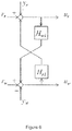
- an embodiment of the present invention provides in an alternative feedthrough of the position error of one stage to the other stage. Such an arrangement is schematically shown in Figure 8 .
- the signal u r is no longer a function of the transfer function H w1 (s), but is merely a function of the reticle stage error and the fed through wafer stage error.
- the stability risk when H r1 (s)H w1 (s) is close to 1 is reduced.
- FIG 10 a fourth embodiment of a control scheme according to an embodiment of the present invention is schematically shown.
- the arrangement of Figure 10 corresponds to the arrangement of Figure 8 , i.e. the actual reticle stage error e rs (i.e. the difference between r r and x rs ) is fed through (via transfer function H w1 (s)) to the wafer stage controller C ws (s) of the wafer stage whereas in Figure 5 , e rs also contained the transferred wafer stage error e ws .
- the actual wafer stage error e ws i.e. the difference between r w and x ws
- the reticle stage controller C rs (s) is fed through (via transfer function H r1 (s) to the reticle stage controller C rs (s).
- control methods according to the present invention provide in an improvement of the positional error observed between two or more stages or bodies or objects that need to operate in synchronism, when compared to the known method of Figure 3 .
- the stability of the known system can be assessed in a similar manner as described above, see equation 3, when considering the controllers C ws (s) and C rs (s) of Figure 3 and the stage system comprising the reticle stage transfer function H rs (s) and the wafer stage transfer function H ws (s) as a respective MIMO (multiple input / multiple output) controller and a SISO (single input / single output) system.
- the MIMO stability is essentially obtained when the SISO transfer functions C ws ( s ) H ws ( s ) and C rs ( s ) H rs ( s ) are stable.
- the closed-loop stability can be considered independent of the feedthrough controller kC rs ( s ) H r 1 ( s ) + kH r 2 ( s ) in equation (11).
- the control device enables a position error between two or more stages that need to operate in synchronism to be reduced.
- the application of the control methods in a lithographic apparatus have been found to significantly reduce the moving average (MA) error between a reticle stage and a wafer stage.
- the moving standard deviation (MSD) error has been found to remain unaffected or slightly improved.
- the description above primary describes a synchronous operation of a reticle stage and a wafer stage in a lithographic apparatus
- the invention may also be applied to improve a synchronised operation of more than two stages and may also be applied outside the field of lithography.
- the control device according to the present invention may also be used to control other stages in a lithographic apparatus, such as stages controlling the position of an optical element or device in the apparatus.
- a lithographic apparatus may also include optical components such as lenses or mirrors or masking blades that need to be positioned, e.g. in synchronism with a stage.
- lithographic apparatus in the manufacture of ICs
- the lithographic apparatus described herein may have other applications, such as the manufacture of integrated optical systems, guidance and detection patterns for magnetic domain memories, flat-panel displays, liquid-crystal displays (LCDs), thin-film magnetic heads, etc.
- LCDs liquid-crystal displays
- any use of the terms “wafer” or “die” herein may be considered as synonymous with the more general terms “substrate” or "target portion”, respectively.
- the substrate referred to herein may be processed, before or after exposure, in for example a track (a tool that typically applies a layer of resist to a substrate and develops the exposed resist), a metrology tool and/or an inspection tool. Where applicable, the disclosure herein may be applied to such and other substrate processing tools. Further, the substrate may be processed more than once, for example in order to create a multi-layer IC, so that the term substrate used herein may also refer to a substrate that already contains multiple processed layers.
- imprint lithography a topography in a patterning device defines the pattern created on a substrate.
- the topography of the patterning device may be pressed into a layer of resist supplied to the substrate whereupon the resist is cured by applying electromagnetic radiation, heat, pressure or a combination thereof.
- the patterning device is moved out of the resist leaving a pattern in it after the resist is cured.
- UV radiation e.g. having a wavelength of or about 365, 248, 193, 157 or 126 nm
- EUV radiation e.g. having a wavelength in the range of 5-20 nm
- particle beams such as ion beams or electron beams.
- lens may refer to any one or combination of various types of optical components, including refractive, reflective, magnetic, electromagnetic and electrostatic optical components.
- the invention may take the form of a computer program containing one or more sequences of machine-readable instructions describing a method as disclosed above, or a data storage medium (e.g. semiconductor memory, magnetic or optical disk) having such a computer program stored therein.
- a data storage medium e.g. semiconductor memory, magnetic or optical disk
Landscapes
- Physics & Mathematics (AREA)
- General Physics & Mathematics (AREA)
- Engineering & Computer Science (AREA)
- Signal Processing (AREA)
- Exposure And Positioning Against Photoresist Photosensitive Materials (AREA)
- Container, Conveyance, Adherence, Positioning, Of Wafer (AREA)
Claims (15)
- Un dispositif de contrôle pour contrôler un positionnement synchrone d'un système multi-corps, le dispositif de contrôle comprenant :une entrée pour recevoir un premier signal d'erreur représentant une différence entre une position souhaitée d'un premier corps du système multi-corps et une position mesurée du premier corps et un deuxième signal d'erreur représentant une différence entre une position souhaitée d'un deuxième corps du système multi-corps et une position mesurée du deuxième corps ;le dispositif de contrôle étant configuré afin de :- déterminer un premier signal d'entraînement primaire pour entraîner un dispositif de positionnement configuré afin d'entraîner le premier corps, sur la base du premier signal d'erreur ;- déterminer un deuxième signal d'entraînement primaire pour entraîner un dispositif de positionnement configuré afin d'entraîner le deuxième corps, sur la base du deuxième signal d'erreur ;- déterminer un premier signal d'entraînement secondaire pour entraîner le dispositif de positionnement configuré afin d'entraîner le premier corps, le premier signal d'entraînement secondaire étant basé sur le deuxième signal d'erreur ; et- déterminer un deuxième signal d'entraînement secondaire pour entraîner le dispositif de positionnement configuré afin d'entraîner le deuxième corps, le deuxième signal d'entraînement secondaire étant basé sur le premier signal d'erreur ;- combiner le premier signal d'entraînement primaire et le premier signal d'entraînement secondaire afin d'obtenir un premier signal d'entraînement combiné et combiner le deuxième signal d'entraînement primaire et le deuxième signal d'entraînement secondaire afin d'obtenir un deuxième signal d'entraînement combiné ;le dispositif de contrôle comprenant en sus une sortie pour sortir le premier signal d'entraînement combiné et le deuxième signal d'entraînement combiné vers les dispositifs de positionnement respectifs,caractérisé en ce que,le dispositif de contrôle est en sus configuré afin de convertir le deuxième signal d'erreur en ce premier signal d'entraînement secondaire à l'aide d'une première fonction de transfert etconvertir le premier signal d'erreur en ce deuxième signal d'entraînement secondaire à l'aide d'une deuxième fonction de transfert.
- Le dispositif de contrôle selon la revendication 1, dans lequel le système multi-corps comprend une pluralité de platines incluant une première platine, la première platine comprenant le premier corps et le dispositif de positionnement configuré afin d'entraîner le premier corps, et une deuxième platine, la deuxième platine comprenant le deuxième objet et le dispositif de positionnement configuré afin d'entraîner le deuxième objet.
- Le dispositif de contrôle selon la revendication 1 ou la revendication 2, dans lequel une relation prédéterminée existe entre la position souhaitée du premier corps et la position souhaitée du deuxième corps.
- Le dispositif de contrôle selon n'importe lesquelles des revendications précédentes, dans lequel le premier signal d'entraînement secondaire n'est pas basé sur le premier signal d'erreur et le deuxième signal d'entraînement secondaire n'est pas basé sur le deuxième signal d'erreur.
- Le dispositif de contrôle selon la revendication 4, dans lequel la première fonction de transfert inclut un modèle fournissant une conversion de position en force pour le premier corps ; et dans lequel la deuxième fonction de transfert inclut un modèle fournissant une conversion de position en force pour le deuxième corps.
- Le dispositif de contrôle selon la revendication 4 ou la revendication 5, dans lequel la première fonction de transfert inclut un premier filtre passe-bas et dans lequel la deuxième fonction de transfert inclut un deuxième filtre passe-bas.
- Le dispositif de contrôle selon la revendication 6, dans lequel le premier signal d'entraînement primaire est en sus déterminé sur la base d'un premier signal de traversée, le premier signal de traversée étant basé sur le deuxième signal d'erreur et dans lequel le deuxième signal d'entraînement primaire est en sus déterminé sur la base d'un deuxième signal de traversée, le deuxième signal de traversée étant basé sur le premier signal d'erreur.
- Le dispositif de contrôle selon la revendication 7, dans lequel le premier signal de traversée est obtenu par un filtrage passe-bas, à l'aide du premier filtre passe-bas, du deuxième signal d'erreur et dans lequel le deuxième signal de traversée est obtenu par un filtrage passe-bas, à l'aide d'un deuxième filtre passe-bas, du premier signal d'erreur.
- Le dispositif de contrôle selon la revendication 6 ou la revendication 8, dans lequel un gain du premier filtre passe-bas multiplié par un gain du deuxième filtre passe-bas est inférieur à 1.
- Le dispositif de contrôle selon la revendication 6 ou la revendication 9, dans lequel le gain du premier filtre passe-bas est inférieur ou égal à 0,8 et dans lequel le gain du deuxième filtre passe-bas est inférieur ou égal à 0,8.
- Le dispositif de contrôle selon n'importe lesquelles des revendications 6 à 9, comprenant un premier organe de contrôle configuré afin de déterminer le premier signal d'entraînement primaire, le premier organe de contrôle comprenant une entrée pour recevoir un premier signal d'entrée comprenant le premier signal d'erreur et le premier signal de traversée et un deuxième organe de contrôle configuré afin de déterminer le deuxième signal d'entraînement primaire, le deuxième organe de contrôle comprenant une entrée pour recevoir un deuxième signal d'entrée comprenant le deuxième signal d'erreur et le deuxième signal de traversée.
- Le dispositif de contrôle selon n'importe quelle revendication précédente, dans lequel le premier signal d'entraînement secondaire est en sus basé sur le premier signal d'erreur et dans lequel le deuxième signal d'entraînement secondaire est en sus basé sur le deuxième signal d'erreur.
- Un système de positionnement multi-platines pour effectuer un positionnement synchrone d'au moins une première platine et une deuxième platine, le système de positionnement multi-platines comprenant :- une première platine configurée afin de porter un premier objet ; la première platine comprenant un dispositif de positionnement configuré afin d'entraîner le premier objet ;- une deuxième platine configurée afin de porter un deuxième objet, la deuxième platine comprenant un dispositif de positionnement configuré afin d'entraîner le deuxième objet ; et- un dispositif de contrôle selon n'importe lesquelles des revendications précédentes pour contrôler un positionnement synchrone du premier objet et du deuxième objet.
- Un appareil lithographique comprenant :un système d'illumination configuré afin de conditionner un faisceau de rayonnement ;une première platine construite afin de supporter un dispositif servant à conformer selon un motif, le dispositif servant à conformer selon un motif étant capable de conférer au faisceau de rayonnement un motif dans sa coupe transversale afin de former un faisceau de rayonnement à motif ;une deuxième platine construite afin de porter un substrat ; etun système de projection configuré afin de projeter le faisceau de rayonnement à motif sur une portion cible du substrat,l'appareil comprenant en sus un dispositif de contrôle selon n'importe lesquelles des revendications 1 à 10 pour contrôler un positionnement synchrone de la première et la deuxième platine.
- Un procédé de fabrication de dispositif comprenant le transfert d'un motif d'un dispositif servant à conformer selon un motif sur un substrat, à l'aide d'un appareil lithographique selon la revendication 14.
Priority Applications (1)
| Application Number | Priority Date | Filing Date | Title |
|---|---|---|---|
| EP14802416.9A EP3084525B1 (fr) | 2013-12-20 | 2014-11-21 | Appareil lithographique et méthode de fabrication d'un dispositif |
Applications Claiming Priority (3)
| Application Number | Priority Date | Filing Date | Title |
|---|---|---|---|
| EP13198925 | 2013-12-20 | ||
| EP14802416.9A EP3084525B1 (fr) | 2013-12-20 | 2014-11-21 | Appareil lithographique et méthode de fabrication d'un dispositif |
| PCT/EP2014/075226 WO2015090841A1 (fr) | 2013-12-20 | 2014-11-21 | Appareil lithographique et procédé de fabrication de dispositif |
Publications (2)
| Publication Number | Publication Date |
|---|---|
| EP3084525A1 EP3084525A1 (fr) | 2016-10-26 |
| EP3084525B1 true EP3084525B1 (fr) | 2019-04-17 |
Family
ID=49880529
Family Applications (1)
| Application Number | Title | Priority Date | Filing Date |
|---|---|---|---|
| EP14802416.9A Active EP3084525B1 (fr) | 2013-12-20 | 2014-11-21 | Appareil lithographique et méthode de fabrication d'un dispositif |
Country Status (9)
| Country | Link |
|---|---|
| US (1) | US10175587B2 (fr) |
| EP (1) | EP3084525B1 (fr) |
| JP (1) | JP6273369B2 (fr) |
| KR (1) | KR101885749B1 (fr) |
| CN (1) | CN105829969B (fr) |
| IL (1) | IL245884B (fr) |
| NL (1) | NL2013842A (fr) |
| TW (1) | TWI537691B (fr) |
| WO (1) | WO2015090841A1 (fr) |
Families Citing this family (3)
| Publication number | Priority date | Publication date | Assignee | Title |
|---|---|---|---|---|
| JP6788839B2 (ja) * | 2016-01-28 | 2020-11-25 | 大日本印刷株式会社 | 荷電粒子ビーム描画装置、荷電粒子ビーム描画システムおよび描画データ生成方法 |
| EP4134744A1 (fr) | 2021-08-09 | 2023-02-15 | ASML Netherlands B.V. | Procédé de positionnement de capteur, système de positionnement, appareil lithographique, appareil de métrologie, et procédé de fabrication d'un dispositif |
| EP4567514A3 (fr) * | 2025-03-27 | 2026-01-07 | ASML Netherlands B.V. | Commande de position d'un appareil d'exposition |
Citations (1)
| Publication number | Priority date | Publication date | Assignee | Title |
|---|---|---|---|---|
| US20030164930A1 (en) * | 2002-02-26 | 2003-09-04 | Canon Kabushiki Kaisha | Stage alignment apparatus and its control method, exposure apparatus, and semiconductor device manufacturing method |
Family Cites Families (12)
| Publication number | Priority date | Publication date | Assignee | Title |
|---|---|---|---|---|
| US5699145A (en) | 1993-07-14 | 1997-12-16 | Nikon Corporation | Scanning type exposure apparatus |
| JPH08241126A (ja) * | 1995-03-02 | 1996-09-17 | Canon Inc | 同期位置制御方法および装置 |
| JP2000000786A (ja) | 1998-06-16 | 2000-01-07 | Komatsu Ltd | 同期制御装置 |
| TW394862B (en) * | 1998-06-23 | 2000-06-21 | Asm Lithography Bv | Lithographic projection apparatus |
| EP1265104A1 (fr) * | 2001-06-06 | 2002-12-11 | ASML Netherlands B.V. | Appareil lithographique, procédé por la production d'un dispositif et dispositif produit par ce procédé |
| JP2005051197A (ja) * | 2003-07-17 | 2005-02-24 | Nikon Corp | ステージ制御方法及び装置、ステージ制御プログラム、露光装置、並びにデバイス製造方法 |
| US7084958B2 (en) * | 2004-04-14 | 2006-08-01 | Asml Netherlands B.V. | Lithographic apparatus, control system and device manufacturing method |
| US20080109178A1 (en) | 2006-11-03 | 2008-05-08 | Nikon Corporation | Method and system for predicting and correcting signal fluctuations of an interferometric measuring apparatus |
| US8451431B2 (en) | 2009-01-27 | 2013-05-28 | Nikon Corporation | Control systems and methods applying iterative feedback tuning for feed-forward and synchronization control of microlithography stages and the like |
| JP5235707B2 (ja) | 2009-02-03 | 2013-07-10 | キヤノン株式会社 | 制御装置 |
| JP2011086892A (ja) * | 2009-10-19 | 2011-04-28 | Canon Inc | 位置制御装置、露光装置およびデバイス製造方法 |
| CN103135357B (zh) | 2011-11-25 | 2015-04-15 | 上海微电子装备有限公司 | 工件台和掩模台的同步控制方法及其系统 |
-
2014
- 2014-11-21 KR KR1020167018885A patent/KR101885749B1/ko active Active
- 2014-11-21 JP JP2016541564A patent/JP6273369B2/ja active Active
- 2014-11-21 CN CN201480069190.0A patent/CN105829969B/zh active Active
- 2014-11-21 EP EP14802416.9A patent/EP3084525B1/fr active Active
- 2014-11-21 WO PCT/EP2014/075226 patent/WO2015090841A1/fr not_active Ceased
- 2014-11-21 US US15/100,920 patent/US10175587B2/en active Active
- 2014-11-21 NL NL2013842A patent/NL2013842A/en unknown
- 2014-12-09 TW TW103142897A patent/TWI537691B/zh active
-
2016
- 2016-05-26 IL IL245884A patent/IL245884B/en active IP Right Grant
Patent Citations (1)
| Publication number | Priority date | Publication date | Assignee | Title |
|---|---|---|---|---|
| US20030164930A1 (en) * | 2002-02-26 | 2003-09-04 | Canon Kabushiki Kaisha | Stage alignment apparatus and its control method, exposure apparatus, and semiconductor device manufacturing method |
Also Published As
| Publication number | Publication date |
|---|---|
| US20160299442A1 (en) | 2016-10-13 |
| KR101885749B1 (ko) | 2018-08-06 |
| JP6273369B2 (ja) | 2018-01-31 |
| EP3084525A1 (fr) | 2016-10-26 |
| JP2017502346A (ja) | 2017-01-19 |
| CN105829969B (zh) | 2019-01-04 |
| TW201527903A (zh) | 2015-07-16 |
| US10175587B2 (en) | 2019-01-08 |
| IL245884B (en) | 2020-07-30 |
| CN105829969A (zh) | 2016-08-03 |
| KR20160098405A (ko) | 2016-08-18 |
| WO2015090841A1 (fr) | 2015-06-25 |
| TWI537691B (zh) | 2016-06-11 |
| NL2013842A (en) | 2015-06-26 |
| IL245884A0 (en) | 2016-07-31 |
Similar Documents
| Publication | Publication Date | Title |
|---|---|---|
| EP1882985B1 (fr) | Appareil lithographique et procédé de fabrication du dispositif | |
| US8300208B2 (en) | Lithographic apparatus and a method to compensate for the effect of disturbances on the projection system of a lithographic apparatus | |
| US8064151B2 (en) | Lithographic apparatus and thermal optical manipulator control method | |
| EP1978409A1 (fr) | Appareil lithographique et procédé de fabrication du dispositif | |
| US9715182B2 (en) | Lithographic apparatus, substrate support system, device manufacturing method and control program | |
| US9671702B2 (en) | Positioning system, a lithographic apparatus and a method for positional control | |
| US7525638B2 (en) | Lithographic apparatus and device manufacturing method | |
| CN101566854A (zh) | 位置控制系统、光刻设备及控制可移动物体的位置的方法 | |
| US9927721B2 (en) | Object positioning system, control system, lithographic apparatus, object positioning method and device manufacturing method | |
| US7256866B2 (en) | Lithographic apparatus and device manufacturing method | |
| EP3084525B1 (fr) | Appareil lithographique et méthode de fabrication d'un dispositif | |
| US7084958B2 (en) | Lithographic apparatus, control system and device manufacturing method | |
| CN102298269B (zh) | 测量系统、方法和光刻设备 | |
| US9977341B2 (en) | Lithographic apparatus and device manufacturing method | |
| WO2016202519A1 (fr) | Système de commande, système de positionnement, appareil lithographique et procédé de fabrication de dispositif | |
| US7352436B2 (en) | Lithographic apparatus, projection apparatus and device manufacturing method | |
| US11454938B2 (en) | Control system, method to increase a bandwidth of a control system, and lithographic apparatus | |
| EP1801657A1 (fr) | Procédé de fabrication d'un dispositif et programme d'ordinateur | |
| WO2019076525A1 (fr) | Moteur, étage à deux temps et appareil lithographique | |
| KR101428606B1 (ko) | 리소그래피 장치 및 디바이스 제조 방법 | |
| NL2020279A (en) | Lithographic Apparatus Imaging Error Correction |
Legal Events
| Date | Code | Title | Description |
|---|---|---|---|
| PUAI | Public reference made under article 153(3) epc to a published international application that has entered the european phase |
Free format text: ORIGINAL CODE: 0009012 |
|
| 17P | Request for examination filed |
Effective date: 20160526 |
|
| AK | Designated contracting states |
Kind code of ref document: A1 Designated state(s): AL AT BE BG CH CY CZ DE DK EE ES FI FR GB GR HR HU IE IS IT LI LT LU LV MC MK MT NL NO PL PT RO RS SE SI SK SM TR |
|
| AX | Request for extension of the european patent |
Extension state: BA ME |
|
| DAX | Request for extension of the european patent (deleted) | ||
| STAA | Information on the status of an ep patent application or granted ep patent |
Free format text: STATUS: EXAMINATION IS IN PROGRESS |
|
| 17Q | First examination report despatched |
Effective date: 20180116 |
|
| GRAP | Despatch of communication of intention to grant a patent |
Free format text: ORIGINAL CODE: EPIDOSNIGR1 |
|
| STAA | Information on the status of an ep patent application or granted ep patent |
Free format text: STATUS: GRANT OF PATENT IS INTENDED |
|
| INTG | Intention to grant announced |
Effective date: 20190102 |
|
| GRAS | Grant fee paid |
Free format text: ORIGINAL CODE: EPIDOSNIGR3 |
|
| GRAA | (expected) grant |
Free format text: ORIGINAL CODE: 0009210 |
|
| STAA | Information on the status of an ep patent application or granted ep patent |
Free format text: STATUS: THE PATENT HAS BEEN GRANTED |
|
| AK | Designated contracting states |
Kind code of ref document: B1 Designated state(s): AL AT BE BG CH CY CZ DE DK EE ES FI FR GB GR HR HU IE IS IT LI LT LU LV MC MK MT NL NO PL PT RO RS SE SI SK SM TR |
|
| REG | Reference to a national code |
Ref country code: GB Ref legal event code: FG4D |
|
| REG | Reference to a national code |
Ref country code: CH Ref legal event code: EP |
|
| REG | Reference to a national code |
Ref country code: DE Ref legal event code: R096 Ref document number: 602014044991 Country of ref document: DE |
|
| REG | Reference to a national code |
Ref country code: AT Ref legal event code: REF Ref document number: 1122227 Country of ref document: AT Kind code of ref document: T Effective date: 20190515 Ref country code: IE Ref legal event code: FG4D |
|
| REG | Reference to a national code |
Ref country code: NL Ref legal event code: MP Effective date: 20190417 |
|
| REG | Reference to a national code |
Ref country code: LT Ref legal event code: MG4D |
|
| PG25 | Lapsed in a contracting state [announced via postgrant information from national office to epo] |
Ref country code: NL Free format text: LAPSE BECAUSE OF FAILURE TO SUBMIT A TRANSLATION OF THE DESCRIPTION OR TO PAY THE FEE WITHIN THE PRESCRIBED TIME-LIMIT Effective date: 20190417 |
|
| PG25 | Lapsed in a contracting state [announced via postgrant information from national office to epo] |
Ref country code: NO Free format text: LAPSE BECAUSE OF FAILURE TO SUBMIT A TRANSLATION OF THE DESCRIPTION OR TO PAY THE FEE WITHIN THE PRESCRIBED TIME-LIMIT Effective date: 20190717 Ref country code: FI Free format text: LAPSE BECAUSE OF FAILURE TO SUBMIT A TRANSLATION OF THE DESCRIPTION OR TO PAY THE FEE WITHIN THE PRESCRIBED TIME-LIMIT Effective date: 20190417 Ref country code: SE Free format text: LAPSE BECAUSE OF FAILURE TO SUBMIT A TRANSLATION OF THE DESCRIPTION OR TO PAY THE FEE WITHIN THE PRESCRIBED TIME-LIMIT Effective date: 20190417 Ref country code: PT Free format text: LAPSE BECAUSE OF FAILURE TO SUBMIT A TRANSLATION OF THE DESCRIPTION OR TO PAY THE FEE WITHIN THE PRESCRIBED TIME-LIMIT Effective date: 20190817 Ref country code: ES Free format text: LAPSE BECAUSE OF FAILURE TO SUBMIT A TRANSLATION OF THE DESCRIPTION OR TO PAY THE FEE WITHIN THE PRESCRIBED TIME-LIMIT Effective date: 20190417 Ref country code: AL Free format text: LAPSE BECAUSE OF FAILURE TO SUBMIT A TRANSLATION OF THE DESCRIPTION OR TO PAY THE FEE WITHIN THE PRESCRIBED TIME-LIMIT Effective date: 20190417 Ref country code: LT Free format text: LAPSE BECAUSE OF FAILURE TO SUBMIT A TRANSLATION OF THE DESCRIPTION OR TO PAY THE FEE WITHIN THE PRESCRIBED TIME-LIMIT Effective date: 20190417 Ref country code: HR Free format text: LAPSE BECAUSE OF FAILURE TO SUBMIT A TRANSLATION OF THE DESCRIPTION OR TO PAY THE FEE WITHIN THE PRESCRIBED TIME-LIMIT Effective date: 20190417 |
|
| PG25 | Lapsed in a contracting state [announced via postgrant information from national office to epo] |
Ref country code: PL Free format text: LAPSE BECAUSE OF FAILURE TO SUBMIT A TRANSLATION OF THE DESCRIPTION OR TO PAY THE FEE WITHIN THE PRESCRIBED TIME-LIMIT Effective date: 20190417 Ref country code: GR Free format text: LAPSE BECAUSE OF FAILURE TO SUBMIT A TRANSLATION OF THE DESCRIPTION OR TO PAY THE FEE WITHIN THE PRESCRIBED TIME-LIMIT Effective date: 20190718 Ref country code: LV Free format text: LAPSE BECAUSE OF FAILURE TO SUBMIT A TRANSLATION OF THE DESCRIPTION OR TO PAY THE FEE WITHIN THE PRESCRIBED TIME-LIMIT Effective date: 20190417 Ref country code: BG Free format text: LAPSE BECAUSE OF FAILURE TO SUBMIT A TRANSLATION OF THE DESCRIPTION OR TO PAY THE FEE WITHIN THE PRESCRIBED TIME-LIMIT Effective date: 20190717 Ref country code: RS Free format text: LAPSE BECAUSE OF FAILURE TO SUBMIT A TRANSLATION OF THE DESCRIPTION OR TO PAY THE FEE WITHIN THE PRESCRIBED TIME-LIMIT Effective date: 20190417 |
|
| REG | Reference to a national code |
Ref country code: AT Ref legal event code: MK05 Ref document number: 1122227 Country of ref document: AT Kind code of ref document: T Effective date: 20190417 |
|
| PG25 | Lapsed in a contracting state [announced via postgrant information from national office to epo] |
Ref country code: IS Free format text: LAPSE BECAUSE OF FAILURE TO SUBMIT A TRANSLATION OF THE DESCRIPTION OR TO PAY THE FEE WITHIN THE PRESCRIBED TIME-LIMIT Effective date: 20190817 |
|
| REG | Reference to a national code |
Ref country code: DE Ref legal event code: R097 Ref document number: 602014044991 Country of ref document: DE |
|
| PG25 | Lapsed in a contracting state [announced via postgrant information from national office to epo] |
Ref country code: CZ Free format text: LAPSE BECAUSE OF FAILURE TO SUBMIT A TRANSLATION OF THE DESCRIPTION OR TO PAY THE FEE WITHIN THE PRESCRIBED TIME-LIMIT Effective date: 20190417 Ref country code: RO Free format text: LAPSE BECAUSE OF FAILURE TO SUBMIT A TRANSLATION OF THE DESCRIPTION OR TO PAY THE FEE WITHIN THE PRESCRIBED TIME-LIMIT Effective date: 20190417 Ref country code: AT Free format text: LAPSE BECAUSE OF FAILURE TO SUBMIT A TRANSLATION OF THE DESCRIPTION OR TO PAY THE FEE WITHIN THE PRESCRIBED TIME-LIMIT Effective date: 20190417 Ref country code: DK Free format text: LAPSE BECAUSE OF FAILURE TO SUBMIT A TRANSLATION OF THE DESCRIPTION OR TO PAY THE FEE WITHIN THE PRESCRIBED TIME-LIMIT Effective date: 20190417 Ref country code: EE Free format text: LAPSE BECAUSE OF FAILURE TO SUBMIT A TRANSLATION OF THE DESCRIPTION OR TO PAY THE FEE WITHIN THE PRESCRIBED TIME-LIMIT Effective date: 20190417 Ref country code: SK Free format text: LAPSE BECAUSE OF FAILURE TO SUBMIT A TRANSLATION OF THE DESCRIPTION OR TO PAY THE FEE WITHIN THE PRESCRIBED TIME-LIMIT Effective date: 20190417 |
|
| PLBE | No opposition filed within time limit |
Free format text: ORIGINAL CODE: 0009261 |
|
| STAA | Information on the status of an ep patent application or granted ep patent |
Free format text: STATUS: NO OPPOSITION FILED WITHIN TIME LIMIT |
|
| PG25 | Lapsed in a contracting state [announced via postgrant information from national office to epo] |
Ref country code: IT Free format text: LAPSE BECAUSE OF FAILURE TO SUBMIT A TRANSLATION OF THE DESCRIPTION OR TO PAY THE FEE WITHIN THE PRESCRIBED TIME-LIMIT Effective date: 20190417 Ref country code: SM Free format text: LAPSE BECAUSE OF FAILURE TO SUBMIT A TRANSLATION OF THE DESCRIPTION OR TO PAY THE FEE WITHIN THE PRESCRIBED TIME-LIMIT Effective date: 20190417 |
|
| 26N | No opposition filed |
Effective date: 20200120 |
|
| PG25 | Lapsed in a contracting state [announced via postgrant information from national office to epo] |
Ref country code: TR Free format text: LAPSE BECAUSE OF FAILURE TO SUBMIT A TRANSLATION OF THE DESCRIPTION OR TO PAY THE FEE WITHIN THE PRESCRIBED TIME-LIMIT Effective date: 20190417 |
|
| PG25 | Lapsed in a contracting state [announced via postgrant information from national office to epo] |
Ref country code: SI Free format text: LAPSE BECAUSE OF FAILURE TO SUBMIT A TRANSLATION OF THE DESCRIPTION OR TO PAY THE FEE WITHIN THE PRESCRIBED TIME-LIMIT Effective date: 20190417 |
|
| REG | Reference to a national code |
Ref country code: CH Ref legal event code: PL |
|
| PG25 | Lapsed in a contracting state [announced via postgrant information from national office to epo] |
Ref country code: MC Free format text: LAPSE BECAUSE OF FAILURE TO SUBMIT A TRANSLATION OF THE DESCRIPTION OR TO PAY THE FEE WITHIN THE PRESCRIBED TIME-LIMIT Effective date: 20190417 Ref country code: LU Free format text: LAPSE BECAUSE OF NON-PAYMENT OF DUE FEES Effective date: 20191121 Ref country code: CH Free format text: LAPSE BECAUSE OF NON-PAYMENT OF DUE FEES Effective date: 20191130 Ref country code: LI Free format text: LAPSE BECAUSE OF NON-PAYMENT OF DUE FEES Effective date: 20191130 |
|
| REG | Reference to a national code |
Ref country code: BE Ref legal event code: MM Effective date: 20191130 |
|
| GBPC | Gb: european patent ceased through non-payment of renewal fee |
Effective date: 20191121 |
|
| PG25 | Lapsed in a contracting state [announced via postgrant information from national office to epo] |
Ref country code: GB Free format text: LAPSE BECAUSE OF NON-PAYMENT OF DUE FEES Effective date: 20191121 Ref country code: IE Free format text: LAPSE BECAUSE OF NON-PAYMENT OF DUE FEES Effective date: 20191121 |
|
| PG25 | Lapsed in a contracting state [announced via postgrant information from national office to epo] |
Ref country code: BE Free format text: LAPSE BECAUSE OF NON-PAYMENT OF DUE FEES Effective date: 20191130 |
|
| PG25 | Lapsed in a contracting state [announced via postgrant information from national office to epo] |
Ref country code: CY Free format text: LAPSE BECAUSE OF FAILURE TO SUBMIT A TRANSLATION OF THE DESCRIPTION OR TO PAY THE FEE WITHIN THE PRESCRIBED TIME-LIMIT Effective date: 20190417 |
|
| PG25 | Lapsed in a contracting state [announced via postgrant information from national office to epo] |
Ref country code: MT Free format text: LAPSE BECAUSE OF FAILURE TO SUBMIT A TRANSLATION OF THE DESCRIPTION OR TO PAY THE FEE WITHIN THE PRESCRIBED TIME-LIMIT Effective date: 20190417 Ref country code: HU Free format text: LAPSE BECAUSE OF FAILURE TO SUBMIT A TRANSLATION OF THE DESCRIPTION OR TO PAY THE FEE WITHIN THE PRESCRIBED TIME-LIMIT; INVALID AB INITIO Effective date: 20141121 |
|
| PG25 | Lapsed in a contracting state [announced via postgrant information from national office to epo] |
Ref country code: MK Free format text: LAPSE BECAUSE OF FAILURE TO SUBMIT A TRANSLATION OF THE DESCRIPTION OR TO PAY THE FEE WITHIN THE PRESCRIBED TIME-LIMIT Effective date: 20190417 |
|
| P01 | Opt-out of the competence of the unified patent court (upc) registered |
Effective date: 20230403 |
|
| PGFP | Annual fee paid to national office [announced via postgrant information from national office to epo] |
Ref country code: DE Payment date: 20251126 Year of fee payment: 12 |
|
| PGFP | Annual fee paid to national office [announced via postgrant information from national office to epo] |
Ref country code: FR Payment date: 20251124 Year of fee payment: 12 |