EP3084843B1 - Quantendetektionselement mit geringem rauschen und verfahren zur herstellung solch eines lichtdetektionselements - Google Patents
Quantendetektionselement mit geringem rauschen und verfahren zur herstellung solch eines lichtdetektionselements Download PDFInfo
- Publication number
- EP3084843B1 EP3084843B1 EP14825129.1A EP14825129A EP3084843B1 EP 3084843 B1 EP3084843 B1 EP 3084843B1 EP 14825129 A EP14825129 A EP 14825129A EP 3084843 B1 EP3084843 B1 EP 3084843B1
- Authority
- EP
- European Patent Office
- Prior art keywords
- layer
- wavelength
- semi
- conducting material
- radiative
- Prior art date
- Legal status (The legal status is an assumption and is not a legal conclusion. Google has not performed a legal analysis and makes no representation as to the accuracy of the status listed.)
- Active
Links
Images





Classifications
-
- H—ELECTRICITY
- H10—SEMICONDUCTOR DEVICES; ELECTRIC SOLID-STATE DEVICES NOT OTHERWISE PROVIDED FOR
- H10F—INORGANIC SEMICONDUCTOR DEVICES SENSITIVE TO INFRARED RADIATION, LIGHT, ELECTROMAGNETIC RADIATION OF SHORTER WAVELENGTH OR CORPUSCULAR RADIATION
- H10F77/00—Constructional details of devices covered by this subclass
- H10F77/40—Optical elements or arrangements
- H10F77/413—Optical elements or arrangements directly associated or integrated with the devices, e.g. back reflectors
-
- H—ELECTRICITY
- H10—SEMICONDUCTOR DEVICES; ELECTRIC SOLID-STATE DEVICES NOT OTHERWISE PROVIDED FOR
- H10F—INORGANIC SEMICONDUCTOR DEVICES SENSITIVE TO INFRARED RADIATION, LIGHT, ELECTROMAGNETIC RADIATION OF SHORTER WAVELENGTH OR CORPUSCULAR RADIATION
- H10F30/00—Individual radiation-sensitive semiconductor devices in which radiation controls the flow of current through the devices, e.g. photodetectors
- H10F30/20—Individual radiation-sensitive semiconductor devices in which radiation controls the flow of current through the devices, e.g. photodetectors the devices having potential barriers, e.g. phototransistors
- H10F30/21—Individual radiation-sensitive semiconductor devices in which radiation controls the flow of current through the devices, e.g. photodetectors the devices having potential barriers, e.g. phototransistors the devices being sensitive to infrared, visible or ultraviolet radiation
- H10F30/22—Individual radiation-sensitive semiconductor devices in which radiation controls the flow of current through the devices, e.g. photodetectors the devices having potential barriers, e.g. phototransistors the devices being sensitive to infrared, visible or ultraviolet radiation the devices having only one potential barrier, e.g. photodiodes
- H10F30/222—Individual radiation-sensitive semiconductor devices in which radiation controls the flow of current through the devices, e.g. photodetectors the devices having potential barriers, e.g. phototransistors the devices being sensitive to infrared, visible or ultraviolet radiation the devices having only one potential barrier, e.g. photodiodes the potential barrier being a PN heterojunction
-
- H—ELECTRICITY
- H10—SEMICONDUCTOR DEVICES; ELECTRIC SOLID-STATE DEVICES NOT OTHERWISE PROVIDED FOR
- H10F—INORGANIC SEMICONDUCTOR DEVICES SENSITIVE TO INFRARED RADIATION, LIGHT, ELECTROMAGNETIC RADIATION OF SHORTER WAVELENGTH OR CORPUSCULAR RADIATION
- H10F30/00—Individual radiation-sensitive semiconductor devices in which radiation controls the flow of current through the devices, e.g. photodetectors
- H10F30/20—Individual radiation-sensitive semiconductor devices in which radiation controls the flow of current through the devices, e.g. photodetectors the devices having potential barriers, e.g. phototransistors
- H10F30/21—Individual radiation-sensitive semiconductor devices in which radiation controls the flow of current through the devices, e.g. photodetectors the devices having potential barriers, e.g. phototransistors the devices being sensitive to infrared, visible or ultraviolet radiation
- H10F30/22—Individual radiation-sensitive semiconductor devices in which radiation controls the flow of current through the devices, e.g. photodetectors the devices having potential barriers, e.g. phototransistors the devices being sensitive to infrared, visible or ultraviolet radiation the devices having only one potential barrier, e.g. photodiodes
- H10F30/223—Individual radiation-sensitive semiconductor devices in which radiation controls the flow of current through the devices, e.g. photodetectors the devices having potential barriers, e.g. phototransistors the devices being sensitive to infrared, visible or ultraviolet radiation the devices having only one potential barrier, e.g. photodiodes the potential barrier being a PIN barrier
-
- H—ELECTRICITY
- H10—SEMICONDUCTOR DEVICES; ELECTRIC SOLID-STATE DEVICES NOT OTHERWISE PROVIDED FOR
- H10F—INORGANIC SEMICONDUCTOR DEVICES SENSITIVE TO INFRARED RADIATION, LIGHT, ELECTROMAGNETIC RADIATION OF SHORTER WAVELENGTH OR CORPUSCULAR RADIATION
- H10F77/00—Constructional details of devices covered by this subclass
- H10F77/10—Semiconductor bodies
- H10F77/12—Active materials
- H10F77/124—Active materials comprising only Group III-V materials, e.g. GaAs
-
- H—ELECTRICITY
- H10—SEMICONDUCTOR DEVICES; ELECTRIC SOLID-STATE DEVICES NOT OTHERWISE PROVIDED FOR
- H10F—INORGANIC SEMICONDUCTOR DEVICES SENSITIVE TO INFRARED RADIATION, LIGHT, ELECTROMAGNETIC RADIATION OF SHORTER WAVELENGTH OR CORPUSCULAR RADIATION
- H10F77/00—Constructional details of devices covered by this subclass
- H10F77/10—Semiconductor bodies
- H10F77/12—Active materials
- H10F77/124—Active materials comprising only Group III-V materials, e.g. GaAs
- H10F77/1248—Active materials comprising only Group III-V materials, e.g. GaAs having three or more elements, e.g. GaAlAs, InGaAs or InGaAsP
-
- H—ELECTRICITY
- H10—SEMICONDUCTOR DEVICES; ELECTRIC SOLID-STATE DEVICES NOT OTHERWISE PROVIDED FOR
- H10F—INORGANIC SEMICONDUCTOR DEVICES SENSITIVE TO INFRARED RADIATION, LIGHT, ELECTROMAGNETIC RADIATION OF SHORTER WAVELENGTH OR CORPUSCULAR RADIATION
- H10F77/00—Constructional details of devices covered by this subclass
- H10F77/10—Semiconductor bodies
- H10F77/14—Shape of semiconductor bodies; Shapes, relative sizes or dispositions of semiconductor regions within semiconductor bodies
- H10F77/143—Shape of semiconductor bodies; Shapes, relative sizes or dispositions of semiconductor regions within semiconductor bodies comprising quantum structures
-
- Y—GENERAL TAGGING OF NEW TECHNOLOGICAL DEVELOPMENTS; GENERAL TAGGING OF CROSS-SECTIONAL TECHNOLOGIES SPANNING OVER SEVERAL SECTIONS OF THE IPC; TECHNICAL SUBJECTS COVERED BY FORMER USPC CROSS-REFERENCE ART COLLECTIONS [XRACs] AND DIGESTS
- Y02—TECHNOLOGIES OR APPLICATIONS FOR MITIGATION OR ADAPTATION AGAINST CLIMATE CHANGE
- Y02E—REDUCTION OF GREENHOUSE GAS [GHG] EMISSIONS, RELATED TO ENERGY GENERATION, TRANSMISSION OR DISTRIBUTION
- Y02E10/00—Energy generation through renewable energy sources
- Y02E10/50—Photovoltaic [PV] energy
- Y02E10/544—Solar cells from Group III-V materials
-
- Y—GENERAL TAGGING OF NEW TECHNOLOGICAL DEVELOPMENTS; GENERAL TAGGING OF CROSS-SECTIONAL TECHNOLOGIES SPANNING OVER SEVERAL SECTIONS OF THE IPC; TECHNICAL SUBJECTS COVERED BY FORMER USPC CROSS-REFERENCE ART COLLECTIONS [XRACs] AND DIGESTS
- Y02—TECHNOLOGIES OR APPLICATIONS FOR MITIGATION OR ADAPTATION AGAINST CLIMATE CHANGE
- Y02P—CLIMATE CHANGE MITIGATION TECHNOLOGIES IN THE PRODUCTION OR PROCESSING OF GOODS
- Y02P70/00—Climate change mitigation technologies in the production process for final industrial or consumer products
- Y02P70/50—Manufacturing or production processes characterised by the final manufactured product
Definitions
- the present invention relates to a very low noise quantum photodetection element and a method of manufacturing such a photodetection element.
- the invention applies in particular to the design of infrared photodetectors with very good sensitivity.
- An optical detector converts optical radiation into an electrical signal.
- This photon-electron conversion can be indirect: in the case of thermal detectors for example, the absorption of light results in a rise in temperature of an absorbing material which is then converted into an electrical signal.
- photonic (or quantum) detectors involve the direct creation of electric charges which can be either ejected (photoemissive effect) or released within the photosensitive material (case of semiconductor materials).
- Photoresistors or LDR: Light Dependent Resistor
- Photodiodes comprise a layer of semiconductor material; they behave like resistors which let pass a more or less large electric current according to the luminous illumination.
- Photodiodes are crossed junction diodes with electric polarization given by an electric current depending on the light illumination. They include, for example, a P-type doped semiconductor and an N-type doped semiconductor which form a junction at their interface (so-called PN junction). N-type doping is achieved by introducing electron donor impurities into the crystal which increase the density of negative charges (electrons).
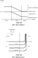
- FIG. 1A shows the energy diagram of electrons in a PN junction. In the vicinity of the junction, there is a depletion zone (absence of free carriers) also called space charge zone (ZCE). Photons with an energy greater than the energy of the semiconductor band gap (“gap”), that is to say of wavelength less than a so-called cut-off wavelength ( ⁇ c ), are absorbed and induce the passage of an electron from the valence band to the conduction band which results in the appearance of a pair of additional mobile charges: an electron in the conduction band and a hole in the valence band .
- gap energy of the semiconductor band gap
- ⁇ c cut-off wavelength
- the figure 1B shows the current / voltage characteristic of a photodiode illuminated by a luminous flux E which can take several values E 1 , E 2 , E 3 such that E 1 ⁇ E 2 ⁇ E 3 .
- the intensity I corresponds to the intensity of the electric current which crosses it as a function of the voltage V at its terminals.
- the particularity of a photodiode is that its current / voltage characteristic depends on the luminous flux that it receives. In the absence of illumination, the characteristic is that of a junction diode with in particular a zero current for a zero applied voltage. As the luminous flux increases, there is an increase in current towards negative intensities, especially for negative voltages.
- the dipole receives energy and functions as a receiver. If the product is negative, the dipole provides energy; it behaves like a generator.
- the generator quadrant corresponds to the photovoltaic field.
- the device When the dipole functions as a receiver, the device is characterized by its detectivity: with ⁇ ext the quantum efficiency of the device and j obs the dark current density, the dark current being defined as the electric current of the photodetector in the absence of light illumination.
- the main sources of dark current are on the one hand intrinsic sources, such as the diffusion current of minority carriers and the radiative and non-radiative generation-recombination current of the charges, and on the other hand sources linked to the manufacturing process, such as non-radiative recombination currents on semiconductor faults (so-called SRH current), which are particularly intense at neighborhood of surfaces or interfaces.
- the diffusion current of the minority carriers is proportional to the gradient of their density, itself imposed by the boundary conditions at the edge of the ZCE on the one hand and of the electrical contact on the other.
- the electrons or the holes are not distributed uniformly in the semiconductor, their movement takes place in a direction which tends to make their spatial distribution uniform.
- the distribution of minority carriers in the doped areas is not uniform, hence diffusion of these carriers.
- the resulting current is called the diffusion current.
- the figure 2 thus describes a quantum detector according to the prior art, comprising a heterojunction 1 of the PIN type composed of three layers 14, 10, 12 of semiconductor material, for example a heterojunction of the InP / InGaAs type.
- Layer 10, for example in InGaAs, located between layers 14 and 12, for example in InP, is a layer of semiconductor material absorbing in the spectral band of interest and forms zone I of the PIN junction.
- the thickness of the absorbent layer 10 is about 2 ⁇ m or more, to absorb all of the incident radiation.
- P-type zones 16 are obtained by diffusion or ion implantation in barrier layer 14. Each P-type zone thus defines a pixel of the detector. Passivation layers 6 on the rear face make it possible to limit the effects of crystallinity defects at the origin of the SRH (Shockley-Read-Hall) current in the space charge zone.
- Each electrical contact 3 is in contact with a read circuit 9 via an indium bead 7.
- the electrical contact 3 represents for each pixel the anode of the electrical circuit formed by the heterojunction.
- the cathode of the circuit is formed by a remote contact 5 in electrical contact with the barrier layer 12 and allowing contact with the read circuit.
- the barrier layer 12 forming the front face FF intended to receive the incident radiation is covered with an antireflection layer 8 in order to transmit to the heterojunction the maximum of the incident optical flow (represented by arrows on the figure 2 ).
- the decrease in the thickness of the space charge zone also results in a decrease in the absorption of the detector.
- An object of the present invention is to provide a detector having an optimized detectivity by reducing the dark current; this objective is achieved by means of an optical resonator, the particular arrangement of which allows a drastic reduction in the phenomena of generation-recombination.
- the wavelength ⁇ rad is the wavelength for which the radiative recombination rate is maximum. It satisfies the equation ⁇ 0 ⁇ rad ⁇ c . By ensuring that there is no resonance at the radiative wavelength, it is ensured that the absorption of the photodetection element is limited to ⁇ rad . The generation-recombination current can then be radically reduced, the emissivity varying like the absorption, according to Kirchoff's law.
- the structure for coupling the incident radiation with the optical cavity is adapted to produce a minimum absorption in the layer of semiconductor material absorbing at the radiative wavelength. According to one variant, this absorption minimum results from antiresonance in the cavity.
- the cut-off wavelength is generally chosen very close to the central wavelength of the detection spectral band in order to limit the rate of radiative recombination and thereby the current of. darkness.
- the cut-off wavelength is intentionally chosen with a given length deviation from the central wavelength of the detection spectral band, the optical cavity exhibiting non-resonance at the radiative wavelength, whose value is strictly between the central wavelength of the detection spectral band and the cut-off wavelength.
- the structure for coupling the incident radiation with the optical cavity is adapted to reduce the absorption in the layer of semiconductor material absorbing at the radiative wavelength ⁇ rad , said reduction being greater than exp ( ⁇ E / kT) where ⁇ E is the variation of the energies corresponding to the wavelengths ⁇ rad and ⁇ o .
- the reduction in absorption is understood here by comparison with an identical detection element in which there is no coupling structure.
- the resonance at the central wavelength of the detection spectral band is localized in the layer of absorbent semiconductor material, making it possible to limit the absorption at the surface and at the interfaces.
- the photodetection element comprises a metallic reflective layer arranged on one side of the optical cavity, opposite to the side supporting the front face.
- the metallic reflective layer also serves as an electrical contact for the photodetection element.
- the resonant optical cavity is a waveguide and the coupling structure comprises a coupling network on the front face and / or a coupling network on the rear face, that is to say on the side of the optical cavity opposite to the side supporting the front face.
- the coupling network (s) can be one or two dimensional, formed by alternating dielectric / dielectric materials (dielectric materials exhibiting refractive indices with different real parts).
- the dielectric material can be an insulator or a semiconductor.
- the coupling network (s) can be limited to the dimensions of one pixel or be extended over a set of pixels.
- the resonance at the central wavelength ⁇ 0 in the layer of absorbent semiconductor material is a guided mode resonance.
- the waveguide exhibits antiresonance at the radiative wavelength ⁇ rad in the layer of absorbent semiconductor material, resulting from destructive interference leading to almost zero absorption.
- the thickness of the waveguide determines the number of resonances in the guide.
- the thickness of the waveguide is between ⁇ 0 / 8n and ⁇ 0 / n, advantageously between ⁇ 0 / 4n and 3 ⁇ 0 / 4n, where n is the average value of the real parts of the refractive indices of the layers made of semiconductor material forming the waveguide.
- the coupling network (s) comprise a periodic structure, with a period between ⁇ 0 / n and ⁇ 0 / n 1 , where n 1 is the real part of the refractive index of the medium of incidence of radiation (eg air).
- n 1 is the real part of the refractive index of the medium of incidence of radiation (eg air).
- the coupling structure comprises “Metal Dielectric Metal” structures otherwise called MDM.
- the photodetection element comprises a stack of layers of semiconductor material forming a heterojunction of PN or PIN type, said stack comprising the layer (s) of semiconductor material forming the optical cavity.
- the heterojunction comprises barrier layers, allowing a strong reduction in the diffusion current.
- At least one of the barrier layers is structured over at least part of its thickness to form a coupling network with the optical cavity.
- the photodetection element according to the first aspect is suitable for detection in one of the bands I, II or III of the infrared.
- the invention relates to an infrared detector comprising an assembly of quantum photodetection elements according to the first aspect.
- the invention relates to methods of manufacturing a quantum detection element according to the first aspect.
- the formation of the epitaxial structure comprises an organometallic epitaxy.
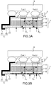
- the figures 3A and 3B show two examples of quantum detectors comprising quantum photodetection elements according to the present description.
- the detector comprises a set of photodetection elements (P 1 , P 2 , ...), arranged for example in a matrix fashion in a focal plane of an imaging optic (not shown).
- the inter-pixel distance is overestimated for reasons of legibility of the figures;
- the elements of photodetection are suitable for the detection of incident radiation in a spectral band centered around a central wavelength ⁇ 0 , for example in one of the bands I, II or III of the infrared, corresponding to the spectral bands of transparency atmospheric.
- the detector comprises a front face FF intended to receive the light radiation, indicated by arrows on the figures 3A and 3B , as well as a reading circuit 9, arranged on the side opposite to the front face.
- Each photodetection element comprises a first electrical contact 3 connected to the reading circuit for example by an indium ball 7 to form as many “pixels” of the detector.
- a second electrical contact 5, common to all the pixels, makes it possible to close the electrical circuit of each of the photo detection elements.
- each photodetection element comprises a stack of layers of semiconductor material forming a PN or PIN type junction 1, with in particular a layer 10 of absorbent semiconductor material with cut-off wavelength ⁇ c > ⁇ 0 .
- the stack of layers of semiconductor material forms a PIN-type heterojunction, the layer 10 of absorbent semiconductor material forming the so-called Intrinsic zone I intentionally undoped.
- the heterojunction examples of which will be described in more detail later, comprises in these examples other layers of semiconductor material including barrier layers 12 and 14, arranged on either side of layer 10.
- Layer 6 can have two complementary roles. On the one hand, it can serve as a passivation layer when the ZCE reaches the detector surface. This is the case for example when the P + doped zones are produced by diffusion or local ionic implantation of dopants (for example zinc) generating a ZCE at the interface of these zones and of the N-type material. case when the pixels are isolated by deep engraving of a mesa. On the other hand, it can serve as protection or encapsulation against attacks from the external environment. This is particularly useful during the hybridization process but is also useful in reducing the effects of long term aging of the detector.
- dopants for example zinc
- the pixels are advantageously electrically isolated from each other, either by etching all or part of the barrier layer 14 between the pixels, or, as will be described in more detail below, by diffusion of atomic hydrogen. in the barrier layer between the pixels, which has the effect of making these areas highly electrically resistive. Since the ZCE is not in contact with the surface of the device, the manufacturing process is thus facilitated and the associated periphery currents of the SRH type are reduced compared to known processes. according to the prior art. Layer 6 can however be retained for its decisive protective role on the aging of the detector.
- each photodetection element further comprises a metallic reflective layer 30 arranged on a face opposite the front face FF intended to receive the incident radiation, as well as a coupling structure 4, for example a coupling network formed of a layer in structured dielectric material.
- a coupling structure 4 for example a coupling network formed of a layer in structured dielectric material. All of the layers of unstructured dielectric material, located between the reflective layer 30 and the entry face, are advantageously chosen to have refractive indices whose real parts are close. They form a resonant optical cavity 2, for example a waveguide, of given thickness e .
- the coupling structure 4 of the incident radiation with the optical cavity formed in the case of Examples 3A and 3B by a coupling network, is adapted to form a resonance at the central wavelength ⁇ 0 corresponding to an almost total absorption (> 80%) localized in the layer of absorbent semiconductor material 10 and reduced absorption in the layer of semiconductor material absorbing at a wavelength ⁇ rad , called radiative wavelength in the present description, and for which the rate of radiative recombination is maximum.
- the rate of radiative recombination R in the layer of semiconductor material is given by the following relation: R ⁇ ⁇ E - E g e - E - E g / kT
- E hc / ⁇ is the energy of the photons emitted at wavelength ⁇ ( h Planck constant and c speed of light)
- k is the Boltzmann constant and T the temperature.
- an absorbing semiconductor material is chosen with a cut-off wavelength ⁇ c strictly greater than the central wavelength of the detection spectral band sought for the photodetection element.
- the length radiative wave which is strictly less than the cut-off wavelength while remaining very close, therefore lies in the strict sense between the resonant wavelength of the optical cavity and the cut-off wavelength ⁇ c absorbent semiconductor material.
- the layer of absorbent semiconductor material can be reduced; it may for example be between a few tens and a few hundred nanometers for an InGaAs layer, making it possible to gain a significant factor in the reduction in thickness compared with the structures of the prior art.
- This reduction in thickness results in a reduction in the thickness of the ZCE which leads to a reduction in the same ratio on the one hand of the radiative recombination currents and on the other hand of the non-radiative recombination currents of the SRH type. . This results in a significant reduction (approximately an order of magnitude) in dark currents.
- an anti-reflective layer is no longer necessary on the front face FF; on the contrary, this is dispensed with in order to maximize the reflection at the interface of the layer of dielectric material 12 with the incident medium (for example air), to generate resonances in the optical cavity.
- the real parts of the refractive indices differ by less than 20% to avoid parasitic reflections at the interfaces.
- the reflective layer 30 of metallic material also contributes to forming the electrical contact 3 which represents for each pixel the anode of the electrical circuit formed by the heterojunction.
- the electrical contact 3 allows contact with the indium ball. It further comprises, optionally, a layer 31 for hybridization with the indium bead.
- the cathode of the circuit is formed by a remote contact 5, the electrical contact 5 comprising for example a layer of conductive material 50 in electrical contact with the barrier layer 12 and a layer of conductive material 51 allowing contact with the read circuit 9 .
- the coupling structure may include a network on the rear face.
- the structuring can be carried out in the metal layer to form the coupling network or in a layer of semiconductor material, for example the barrier layer 14.
- the coupling structure may include a coupling network on the front face.
- the coupling structure can be obtained by depositing a network on the layer of semiconductor material 12, as illustrated in FIG. figure 3B , or directly by structuring the layer of semiconductor material 12.
- the coupling structure can also include a network on the front face and a network on the rear face.
- Other coupling networks are possible, for example metal-dielectric networks.
- the coupling network (s) can be limited to the dimensions of one pixel ( figure 3A ) or be extended over a set of pixels ( figure 3B ).
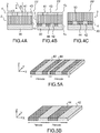
- the figures 4A to 4C thus illustrate different variants of coupling structures suitable for producing a photodetection element according to the present description.
- the layer or layers of dielectric material forming the optical cavity 2 are reduced to the single layer 10. Only the reflective layer 30 is shown, which is in all cases arranged on the rear face.
- the example of figure 4A shows a coupling structure with a single front-facing coupling network.
- the network 4 is transparent or semi-transparent to allow at least part of the radiation to pass, symbolized on the figure 4A by the wave vector k. It is for example a network formed of alternations of two dielectric materials 41 and 43, semiconductor, or insulator, or air, of different indices. Alternatively, it may be an alternation of a metallic material and a dielectric, semiconductor, insulating or air material.
- the figure 4C shows a coupling structure with a single rear panel coupling network.
- the network 4 consists for example of a network formed of alternations of two dielectric materials 42, 44, at least one of which is conductive; it may also be an alternation between a metallic or semiconductor material, and a dielectric material, of the semiconductor, or insulating, or air type.
- the figure 4B represents an example of a coupling structure comprising two networks 4 A and 4 B respectively on the front and rear face.
- the network on the front face is transparent or partially transparent.
- the network on the back comprises at least one conductive material.
- the plurality of networks (2 or more) makes it possible in particular to facilitate the generation of antiresonances.
- the figures 5A to 5E illustrate in the case of coupling networks, several possible forms of networks, with one or two dimensions.
- the coupling structures can comprise structures of the metal-dielectric-metal (MDM) type, as described for example in the patent application FR 2959352 . Note that in the latter case, periodic structuring is not necessary but rather motivated for technological reasons. Indeed, MDM-type structures act individually as nano-antennas.
- MDM metal-dielectric-metal
- the figure 6 illustrates according to a variant, the optical diagram of a detection element according to the present description implementing an optical cavity of waveguide type with a coupling network on the rear face.
- the optical diagram of the detection element thus illustrated comprises a region A corresponding to the medium in which the light radiation is incident (for example air), a region B corresponding to the waveguide, a region C corresponding to the grating coupling and a region D corresponding to the metal mirror.
- the detection element comprises one or more layers of unstructured semiconductor material 10, 12, of thicknesses h B1 , h B2 , forming the waveguide. All the layers, with similar refractive indices, are optically assimilated to a single layer B with a given average index.
- the detection element further comprises a periodic network (region C), with one or two dimensions, of thickness h C , consisting for example on the one hand of the same semiconductor material (s) ( s) 44 as the waveguide, and on the other hand of an electrically insulating dielectric material 42.
- the network is characterized by a period p and a fill factor w / p.
- the detection element comprises a reflective layer 30 (region D), advantageously a layer of metallic material serving both as an ohmic contact and as an optical mirror (for example, gold).
- the resonances used are resonances of guided modes. They take place in the waveguide, and are obtained thanks to the coupling between the incident wave and the modes of the guide. Coupling is provided by the periodic network.
- a thin semiconductor layer surrounded by materials of lower optical index behaves in fact like a waveguide: the wave can propagate according to guided modes, characterized by a phase variation equal to 0 (modulo 2 ⁇ ) after a round trip in the layer (ie between the A / B and B / C interfaces). There is resonance when the wave incident is coupled to one of these modes. The incident energy is then stored in this mode (the photons make several round trips) which increases the components of the electromagnetic field in the guide and consequently the probability of absorption (proportional to the square of the electric field) of the photons thus trapped. .
- coupling structures periodic or not, are introduced on one side and / or the other of the guide. In the example of figure 6 , the coupling is carried out by periodically structuring the rear face of the waveguide so that at least one order diffracted by the grating coincides with at least one mode of the guide.
- the period is chosen such that only three orders (0, +1 and -1) are diffracted by the grating in the waveguide.
- the figure 7 illustrates the exchanges between the incident wave and the two diffraction modes (mode associated with order 0, and mode associated with the symmetrical combination of orders +1 and -1) at normal incidence in the waveguide in the case where the three orders (0, +1 and -1) are diffracted by the grating in the waveguide.
- the resonance is associated with a coupling of mode 0 with the modes (+1, -1) of the waveguide.
- the superposition of the resonances in TE and TM is advantageously obtained by adjusting the phase associated with the reflection coefficient r C / B (m) for the two polarizations with the parameters of the network (period p, filling factor w / p, and thickness h C ).
- the optical resonator of the photodetection element it is sought in the optical resonator of the photodetection element according to the present description, to obtain a Fabry-Perot type resonance in the waveguide at the central wavelength of the detection spectral band and to confine laterally the electric field at resonance in the waveguide thanks to the +1 and -1 orders diffracted by the grating.
- Fabry-Perot resonance appears when the phase accumulated by the fundamental mode in the waveguide after a round trip between the two interfaces (A / B and B / C on the figure 7 ) is equal to 0 (modulo 2pi). It is characterized by the appearance of standing waves in the waveguide, with successions of bellies (field maxima) and nodes (field minimum) in the vertical direction.
- the objective is to have at least one resonance belly in the absorbent layer in order to have a significant absorption, which corresponds to a Fabry-Perot resonance of order 1. In effect, at order 0, there is only one resonance belly, located at the air / waveguide interface; at order 1, there is always this resonance belly, with an additional resonance belly at ⁇ / 2n from the interface. It is this second belly that we want to have at the level of the active layer.
- the electric field in the structure is then characterized by a first resonance belly at the air / waveguide interface, and a second resonance belly at ⁇ 0 / 2n under the first resonance belly.
- the two bellies are confined laterally in a half-period of the network, and are located above the conductive part of the network (metal or semiconductor).
- the electric field is invariant in the horizontal direction (x).
- the lateral confinement of the electric field above the conductive parts of the network further reduces the dark current.
- the applicants have shown that the structuring of the rear face of the heterojunction makes it possible to make the zones situated at the level of the etched parts electrically inactive. As a result, these areas do not generate dark current, ie for a fill factor of 50%, a reduction in the total dark current of 50%.
- the photons absorbed in this region do not generate a photocurrent.
- the figures 8 , 9A and 9B respectively represent the absorption spectrum and the maps of the electric field
- the parameters are optimized for operation of the photodetection element in the infrared I band, around 1.5 ⁇ m, all of the layers of semiconductor material forming a heterojunction of the InGaAs / InP type. More precisely, the numerical simulations are obtained with an electromagnetic simulation code, based for example on the B-Spline modal method (BMM), or the Fourier modal method (FMM).
- BMM B-Spline modal method
- FMM Fourier modal method
- the indices of InGaAs and gold are calculated respectively at the using theoretical formulas given in the articles (Sadao Adachi. Optical dispersion relations for GaP, GaAs, GaSb, InP, InAs, InSb, Al x Ga1- x As, and In1- x Ga x As y P1- y . Journal of Applied Physics, 66 (12): 6030-6040, 1989 ) and Aleksandar D. Rakic, Aleksandra B. Djuri ⁇ ic, Jovan M. Elazar, and Marian L. Majewski.
- the numerical simulations are carried out with the BMM code, based on the B-Spline modal method (see P.Bouchon et al., “Fast modal method for subwavelength gratings based on B-spline formulation”, Journal of the Optical Society of America A, 27 (4): 696-702, 2010 ).
- This same figure shows the absorption spectra 112, 116 calculated only in the layer 10 of semiconductor material.
- the absorption spectra in the optical cavity taken as a whole and the absorption spectra only in layer 10 have a similar behavior for wavelengths below 1.6 ⁇ m.
- the semiconductor layer 10 absorbs and therefore generates the photocurrent. The few differences are due to absorption losses in the metal parts.
- the guided mode resonances are associated with the appearance of standing waves, resulting from the combination of counter-propagating waves (horizontal and vertical) in the waveguide. These interferences are characterized by local extrema of the electric field.
- the figures 9A and 9B illustrate for TE and TM polarizations, the maps of the electric field
- the two resonance bellies (in white in the figures) are confined laterally in a half-period of the network, and are located above the conductive part of the network (metal or semiconductor) in the layer of absorbent semiconductor material .
- the figures 9C and 9D illustrate for TE and TM polarizations, the maps of the electric field
- 2 for the radiative wavelength ⁇ rad 1.62 ⁇ m. On the contrary, an absence of the electric field is observed in the layer of semiconductor material absorbing at the radiative wavelength, resulting from the non-resonance at this wavelength.
- the figure 10 represents a diagram illustrating a particular example of a heterojunction, for example a heterojunction of the InP / InGaAs type suitable for the detection in I-band of the infrared, structured so that one of the barrier layers of the heterojunction has the coupling network function in the simplified optical diagram shown for example on the figure 6 .
- the heterojunction comprises a P-type zone (all of the layers 44, 17, 15, 13), an intrinsic I zone (10) and an N-type zone (all of the layers 11 and 12) to form a PIN junction.
- the intrinsic zone is an absorbing layer made with a semiconductor whose forbidden bandwidth is smaller than the energy of the incident photons.
- the incident wavelength ⁇ 0 is lower than the radiative wavelength ⁇ rad (see equation (3) above) in order to have better absorption but also to be able to spectrally differentiate absorption and radiative emission.
- the intrinsic zone 10 is the active zone of the detection element.
- the intrinsic zone 10 can be formed of a layer of InGaAs having a bandgap energy of 0.74eV for detection at 0.8eV.
- the P-type and N-type zones are composed of heavily doped semiconductor layers, respectively P and N.
- These zones can in particular be formed of several layers, one of which is greater in thickness, forming the body layer, respectively 15 and 44 for the N-type zone and 12 for the P-type zone; the body layer of the ZQN preferably has, a forbidden band width greater than that of the intrinsic zone 10, for example a forbidden bandwidth greater than 10k B T with k B the Boltzmann constant and T the temperature of the device, advantageously of InP.
- the other layers of the doped zones of smaller thicknesses 11, 13 and 17 than the body layers of the N-type and P-type ZQNs are formed from the same material as that of the layer of the intrinsic zone, for example layers of InGaAs.
- the thin layers of InGaAs make it possible, in particular, to obtain good conditions for electronic transport with low contact resistances and better collection of the majority carriers.
- the body layers doped with a band gap markedly greater than that of the intrinsic zone make it possible to reduce the diffusion current linked to the minority carriers.
- the InP layer will have the effect of introducing potential barriers at the InGaAs / InP interface both in the valence band and in the conduction band.
- the potential barrier of the valence band is sufficiently large to reduce the density of electrons injected into the ZQN.
- the gradient of the minority carriers in this zone being reduced in the same ratio, this results in a reduction in the same ratio of the diffusion current.
- the barrier of the conduction band is thin enough so that the electrons can tunnel through, ensuring a thermodynamic equilibrium of the populations of electrons on either side of this barrier.
- the majority carriers are therefore efficiently collected while the diffusion of the minority carriers is greatly reduced (by a factor close to: exp ( ⁇ E g / k B T )), the dark current is therefore reduced without hindering the collection of the current photo.
- Two electrical contact layers 18 and 19 are present in the structure.
- These electrical contacts are made with a semiconductor with a low band gap, for example in InGaAs, to ensure low contact resistance.
- the contact 19 is offset at the edge of the detector or of the array of detectors so as not to create any shading for the incident flux of photons and also to facilitate manufacture.
- the contact is structured as is the barrier on this side.
- the P-doped upper layers are structured by etching over almost all of their thicknesses.
- a layer 17 placed in the upper barrier acts as a stop layer for the etching. It allows the control of the manufacturing process. It has no effect on the dark current.
- Table 2 shows an example of the composition of a hetero semiconductor structure for a low noise quantum detection element as described in the present application.
- the surface current mainly due to the non-radiative recombination processes located at the edge of the device. They are very greatly reduced in this structure by eliminating any contact of the space charge zone (mainly InGaAs) with the free surface of the device. Indeed, the structuring of the upper part of the device leaves a layer of lightly doped large-gap semiconductor (here hydrogenated InP) exhibiting a low surface recombination speed ( ⁇ 5000 cm / s).
- the space charge zone mainly InGaAs
- the structuring of the upper part of the device leaves a layer of lightly doped large-gap semiconductor (here hydrogenated InP) exhibiting a low surface recombination speed ( ⁇ 5000 cm / s).
- the pixels are separated from each other by the same process: etching of the P-type zone up to the InGaAs stop layer.
- etching of the P-type zone up to the InGaAs stop layer it is possible not to etch the P-type zone and to practice diffusion of atomic hydrogen from the surface.
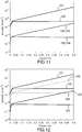
- the figure 11 represents the current-voltage electrical characteristic
- the curves 101, 102 thus represent the current-voltage characteristics of the InGaAs junction, respectively in forward and reverse bias.
- the curves 103, 104 represent the current-voltage characteristics of the InP junction, respectively in forward and reverse bias.
- the curves 105, 106 represent the current-voltage characteristics of the InGaAs / InP heterojunction, respectively in forward and reverse bias.
- the figure 12 represents the current-voltage electrical characteristics calculated for the same structures but this time taking into account the phenomena of radiative recombination. It is observed that the current-voltage characteristics of the InP (curves 103, 104) and InGaAs (curves 101, 102) junctions are similar to those calculated without taking into account the radiative recombinations. In these structures, the diffusion current is dominant. On the other hand, the very strong reduction in the diffusion current in the InGaAs / InP heterojunction makes the contribution of the radiative recombination phenomena dominant (curves 105, 106). The dark current of the InP / InGaAs heterojunction can thus be reduced by about 3 orders of magnitude compared to that of an InGaAs junction.
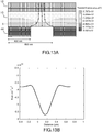
- the figures 13A and 13B illustrate the effect of structuring on the phenomena of radiative generation-recombination.
- the figure 13A presents a mapping of the electrostatic potential in reverse bias (detector operation) in a device similar to that described on the figure 10 , with the parameters described in Table 2.
- the N-type zones (layer 12) have a relatively constant negative potential and the P-type zones (layer 44) have a relatively constant positive potential.
- the potential In the space charge zone (layer 10), the potential varies.
- the arrow lines represent the electric field lines. Under the effect of the strong field which exists at the level of the structured part of the layer 44, the electron hole pairs generated via the intrinsic density are collected by the semiconductor pads.
- the figure 13B represents the modeling of the radiative recombination rate R in reverse polarization as a function of the position in the device according to the cross section S of the figure 13A .
- the rate of recombination is negative.
- a decrease in the rate of radiative recombination centered around 0.2 ⁇ m is observed, which corresponds to the region between the semiconductor pads.
- the effect of structuring on the rate of recombination is thus observed.
- By adjusting the structuring of the network it is possible to change the profile of the recombination rate compared to a flat profile of an unstructured device.
- the figure 14 illustrates the electroluminescence spectrum calculated for an InGaAs / InP heterojunction photodiode as shown in Figure figure 10 , with the parameters given in Table 2 and a forward bias of 0.57 V. This spectrum was measured under high forward voltage to facilitate the experiment. It has been shown experimentally that it depends very little on the voltage applied, in particular its maximum remains fixed at the wavelength ⁇ rad . The figure 14 thus shows the radiative processes at the origin of the dark current as a function of the wavelength (also noted “luminance of the heterostructure”).
- zone I active layer made of absorbent semiconductor material
- the corresponding component of the dark current density is then reduced in the thickness reduction ratio.
- the quantum efficiency of the detector is also reduced.
- the thickness of zone I is advantageously reduced to a compromise value between these two antagonistic effects.
- the dimensioning of the optical resonator (parameters of the cavity and of the coupling structure) is adapted to obtain, at the wavelength ⁇ rad for which the radiative recombination rate is maximum (see equation 2 above), a reduced coupling with the free space so as to increase the life of the carriers in this zone. It is therefore advantageously a matter of placing the detection device within an optical resonator exhibiting a resonance at the detection wavelength ⁇ 0 (maximum coupling with the free space) and an antiresonance (minimum coupling with the free space) at the emission length ⁇ rad .
- the reduction in absorption at ⁇ rad thus produced is in particular, in order to be useful, greater than exp ( ⁇ E / kT) where ⁇ E is the difference in energy between ⁇ rad and ⁇ o .
- the figure 15 represents as a function of the wavelength, the absorption of the cavity averaged over all the angles of incidence (curve 122), the luminance of the heterojunction (curve 120) and the luminance resulting from the cavity, obtained by multiplication of the two spectra.
- the figures 16A to 16G illustrate an exemplary embodiment for the manufacture of a detection element according to the present description, suitable for example for layers of monocrystalline semiconductor material.
- a stack of layers 21, 12, 10, 15, 17 and 44 made of semiconductor material is produced by epitaxy on a suitable substrate 20 (for example in InP).
- a first barrier layer 21 (for example in InGaAs) is epitaxied on the InP substrate.
- the layers 15, 10 and 19 are suitable for producing the desired detector element. These are respectively an N-doped InP layer 15, an intrinsic layer 10 and a P-doped layer 19 to form a PIN junction.
- the intrinsic zone can typically have dimensions of 70 nm.
- the N doping layer 19 can have dimensions typically 200 nm with a carbon doping of typically 3x10 18 cm -3 .
- the n-doping layer 15 may have dimensions typically of 200 nm with a silicon doping of typically 3 ⁇ 10 18 cm -3 .
- a mask 60 is created by lithography on the InP layer 44. This mask makes it possible in particular to define the shape of the coupling networks.
- the InP layer is etched by reactive ion etching and wet etching. The InGaAs layer then serves as a stop layer for the etching. Then, the mask is removed.
- the planarizing resin 42 (dielectric) is coated with a spinner.
- a fifth step ( figure 16E ) reactive ionic etching of the dielectric is carried out until it touches the surface.
- a metallic layer 30 of Au is deposited.
- the sample is transferred to a host substrate by a bonding method (epoxy, anodic bonding, etc.).
- the substrate 2 is removed as far as the stop layer 21 and then the latter is removed by the wet process.
- the epitaxial monocrystalline semiconductor material layers as described in the above process can comprise, for example, layers of gallium arsenide (GaAs) and the associated alloys (for example aluminum and gallium arsenide. AlGaAs), layers of indium phosphide InP and associated alloys (for example gallium indium arsenide InGaAs), layers of gallium antimonide (GaSb) and indium arsenide (InAs), in in particular an InAs / GaSb super-lattice and the associated alloys (for example the gallium and aluminum antimonide AlGaSb), layers of silicon (Si).
- GaAs gallium arsenide
- AlGaAs aluminum and gallium arsenide
- AlGaAs indium phosphide InP and associated alloys
- GaSb gallium antimonide
- InAs indium arsenide
- Si silicon
- the invention applies in the same way to detection in the visible, in particular for photovoltaic applications.
- the photodetection elements suitable for making a device are substantially the same as those described for detection, but they are forward biased.
- the efficiency of converting solar energy into electrical energy is limited by several factors, including the radiative recombinations of the photocarriers. According to the article ( Polman, A., & Atwater, HA (2012). Photonic design principles for ultrahigh-efficiency photovoltaics. Nature materials, 11 (3), 174-177 ), We would thus gain about 7% on the efficiency of solar cells by dispensing with these recombinations.
- the quantum detection element and the method of manufacturing said element include various variants, modifications and improvements which will be evident to those skilled in the art.
Landscapes
- Light Receiving Elements (AREA)
- Photometry And Measurement Of Optical Pulse Characteristics (AREA)
Claims (13)
- Quantenphotodetektionselement (P1, P2, ...) einer einfallenden Strahlung in einem Spektralband, das um eine zentrale Wellenlänge λ0 zentriert ist, mit einer Frontseite (FF), die zum Empfangen der Strahlung bestimmt ist, und das Folgendes umfasst:- einen Stapel von Schichten aus Halbleitermaterial, der einen PN- oder PIN-Übergang bildet und mindestens eine Schicht aus absorbierendem Halbleitermaterial (10) mit einer Grenzwellenlänge λc>λo umfasst, wobei der Stapel von Schichten aus Halbleitermaterial einen optischen Resonanzhohlraum (2) des Wellenleitertyps mit einer gegebenen Dicke (e) bildet;- eine metallische Reflexionsschicht (30), die auf einer Seite des optischen Hohlraums gegenüber der die Frontseite tragenden Seite angeordnet ist und einen optischen Spiegel bildet; und- eine Struktur (4) zum Koppeln der einfallenden Strahlung mit dem optischen Hohlraum, gebildet aus einem Frontseitenbeugungsgitter und/oder einem Rückseitenbeugungsgitter, d.h. auf einer Seite des optischen Hohlraums gegenüber der die Frontseite tragenden Seite,
dadurch gekennzeichnet, dass das Netzwerk aus zwei abwechselnden dielektrischen Materialien gebildet wird und eine(n) gegebene(n) Dicke (hc), Periode (p) und Füllfaktor (w/p) aufweist, bestimmt zum Bilden:∘ einer Geführten-Moden-Resonanz bei der zentralen Wellenlänge λ0, die eine Absorption von mehr als 80 % in der Schicht aus dem absorbierenden Halbleitermaterial bei der zentralen Wellenlänge zulässt;∘ einer Antiresonanz bei der Strahlungswellenlänge λrad in der absorbierenden Halbleitermaterialschicht, um ein Absorptionsminimum in der absorbierenden Halbleitermaterialschicht bei der Strahlungswellenlänge λrad zu erzeugen, worin die Strahlungswellenlänge λrad die Wellenlänge ist, für die bei Betriebstemperatur die Strahlungsrekombinationsrate maximal ist. - Photodetektionselement nach Anspruch 1, wobei sich die Resonanz bei der zentralen Wellenlänge λ0 in der Schicht aus absorbierendem Halbleitermaterial befindet.
- Photodetektionselement nach einem der vorherigen Ansprüche, wobei die Kopplungsstruktur der einfallenden Strahlung mit dem optischen Hohlraum zum Verringern der Absorption in der absorbierenden Halbleitermaterialschicht bei der Strahlungswellenlänge λrad angepasst ist, wobei die Verringerung größer als exp(ΔE/kT) ist, worin ΔE die Variation der Energien entsprechend den Wellenlängen λrad und λ0 ist.
- Photodetektionselement nach einem der vorherigen Ansprüche, wobei die Kopplungsstruktur ein Beugungsgitter auf der Rückseite, d.h. auf einer Seite des optischen Hohlraums gegenüber der die Frontseite tragenden Seite umfasst.
- Photodetektionselement nach einem der vorherigen Ansprüche, wobei die Dicke des Wellenleiters zwischen λ0/8n und λ0/n, vorzugsweise zwischen λ0/4n und 3λ0/4n liegt, worin n der Mittelwert der Realteile der Brechungsindizes der den Wellenleiter bildenden Halbleitermaterialschicht(en) ist.
- Photodetektionselement nach einem der vorherigen Ansprüche, wobei das/die Beugungsgitter eine periodische Struktur mit einer Periode zwischen λ0/n und λ0/n1 umfasst/umfassen, worin n der Mittelwert der Realteile der Brechungsindizes der den Wellenleiter bildenden Halbleitermaterialschicht(en) ist und n1 der Realteil des Brechungsindexes des einfallenden Mediums der Strahlung ist.
- Photodetektionselement nach einem der vorherigen Ansprüche, das einen Stapel von Halbleitermaterialschichten umfasst, die einen Heteroübergang vom PN- oder PIN-Typ bilden, wobei der Stapel die den optischen Hohlraum bildenden Halbleitermaterialschicht(en) umfasst.
- Photodetektionselement nach Anspruch 7, wobei der Heteroübergang Sperrschichten (12, 14) umfasst.
- Photodetektionselement nach Anspruch 8, wobei mindestens eine der Sperrschichten (14) über mindestens einen Teil ihrer Dicke so strukturiert ist, dass sie mit dem optischen Hohlraum ein Beugungsgitter bildet.
- Photodetektionselement nach einem der vorherigen Ansprüche, angepasst zum Detektieren in einem der Infrarotbänder I, II oder III.
- Infrarotdetektor mit einer Anordnung von Quantenphotodetektionselementen nach einem der vorherigen Ansprüche.
- Verfahren zur Herstellung eines Quantendetektionselements nach einem der Ansprüche 1 bis 10, das Folgendes umfasst:- Bilden einer epitaxierten Struktur auf einem Substrat (20), die einen Stapel von Halbleitermaterialschichten, darunter mindestens eine Schicht aus absorbierendem Halbleitermaterial (10) mit einer Grenzwellenlänge λc>λ0, und eine obere Schicht aus dielektrischem Material (44) umfasst,- Strukturieren der oberen Schicht aus dielektrischem Material zum Bilden eines Beugungsgitters,- Absetzen einer metallischen Reflexionsschicht (30) auf dem Beugungsgitter,- Entfernen des Substrats, um die Frontfläche (FF) des Detektionselements zu bilden.
- Herstellungsverfahren nach Anspruch 12, wobei die Bildung der epitaxierten Struktur metallorganische Epitaxie umfasst.
Applications Claiming Priority (2)
| Application Number | Priority Date | Filing Date | Title |
|---|---|---|---|
| FR1362842A FR3015113B1 (fr) | 2013-12-17 | 2013-12-17 | Element de detection quantique a faible bruit et procede de fabrication d'un tel element de photodetection |
| PCT/EP2014/078329 WO2015091709A1 (fr) | 2013-12-17 | 2014-12-17 | Elément de détection quantique à faible bruit et procédé de fabrication d'un tel élément de photodétection |
Publications (2)
| Publication Number | Publication Date |
|---|---|
| EP3084843A1 EP3084843A1 (de) | 2016-10-26 |
| EP3084843B1 true EP3084843B1 (de) | 2021-01-27 |
Family
ID=50729552
Family Applications (1)
| Application Number | Title | Priority Date | Filing Date |
|---|---|---|---|
| EP14825129.1A Active EP3084843B1 (de) | 2013-12-17 | 2014-12-17 | Quantendetektionselement mit geringem rauschen und verfahren zur herstellung solch eines lichtdetektionselements |
Country Status (6)
| Country | Link |
|---|---|
| US (1) | US9755090B2 (de) |
| EP (1) | EP3084843B1 (de) |
| JP (1) | JP2017500743A (de) |
| CN (1) | CN105981179B (de) |
| FR (1) | FR3015113B1 (de) |
| WO (1) | WO2015091709A1 (de) |
Cited By (1)
| Publication number | Priority date | Publication date | Assignee | Title |
|---|---|---|---|---|
| EP4268281B1 (de) * | 2020-12-23 | 2025-02-26 | Thales | Integration einer detektionsschaltung auf der basis von optischen resonatoren, die mit einer ausleseschaltung eines bildaufnehmers verbunden sind |
Families Citing this family (13)
| Publication number | Priority date | Publication date | Assignee | Title |
|---|---|---|---|---|
| FR3015113B1 (fr) * | 2013-12-17 | 2018-06-01 | Centre National De La Recherche Scientifique- Cnrs | Element de detection quantique a faible bruit et procede de fabrication d'un tel element de photodetection |
| EP3261130B1 (de) * | 2016-06-20 | 2020-11-18 | ams AG | Photodetektorvorrichtung mit integriertem kontrastreichem gitterpolarisator |
| FR3069956B1 (fr) * | 2017-08-03 | 2019-09-06 | Thales | Detecteur infrarouge ameliore |
| JP7052362B2 (ja) * | 2018-01-16 | 2022-04-12 | 日本電気株式会社 | 赤外線検出素子、赤外線検出器及び赤外線検出素子の製造方法 |
| FI3769343T3 (fi) * | 2018-03-22 | 2023-09-01 | Iee Sa | Valoilmaisin |
| FR3083645B1 (fr) | 2018-07-05 | 2020-07-31 | Thales Sa | Detecteur bi-spectral ameliore |
| CN109411500B (zh) | 2018-10-31 | 2021-01-22 | 京东方科技集团股份有限公司 | 探测面板及其制作方法 |
| US12185018B2 (en) * | 2019-06-28 | 2024-12-31 | Apple Inc. | Stacked electromagnetic radiation sensors for visible image sensing and infrared depth sensing, or for visible image sensing and infrared image sensing |
| TWI835924B (zh) * | 2019-11-18 | 2024-03-21 | 晶元光電股份有限公司 | 光偵測元件 |
| TWI872948B (zh) * | 2019-11-18 | 2025-02-11 | 晶元光電股份有限公司 | 光偵測元件 |
| FR3141283A1 (fr) * | 2022-10-20 | 2024-04-26 | Thales | Procédé de fabrication de photodiodes à hétérojonctions durcies aux irradiations |
| CN117293225B (zh) * | 2023-10-19 | 2026-03-17 | 山西中来光能电池科技有限公司 | 一种具有局域等离激元结构的晶体硅太阳电池及其制备方法 |
| FR3155601A1 (fr) * | 2023-11-22 | 2025-05-23 | Commissariat A L'energie Atomique Et Aux Energies Alternatives | Dispositif optique |
Family Cites Families (9)
| Publication number | Priority date | Publication date | Assignee | Title |
|---|---|---|---|---|
| US5455421A (en) * | 1985-08-13 | 1995-10-03 | Massachusetts Institute Of Technology | Infrared detector using a resonant optical cavity for enhanced absorption |
| FR2741483B1 (fr) * | 1995-11-21 | 1998-01-02 | Thomson Csf | Dispositif optoelectronique a puits quantiques |
| FR2748604B1 (fr) * | 1996-05-13 | 1998-08-07 | Commissariat Energie Atomique | Photodetecteur a structure optique resonnante avec un reseau |
| US6055262A (en) * | 1997-06-11 | 2000-04-25 | Honeywell Inc. | Resonant reflector for improved optoelectronic device performance and enhanced applicability |
| EP1192662A1 (de) * | 1999-06-25 | 2002-04-03 | California Institute Of Technology | Mehrdirektionale strahlungseinkopplung in quantentopf-infrarotdetektoren |
| JP2008288293A (ja) * | 2007-05-16 | 2008-11-27 | Nippon Telegr & Teleph Corp <Ntt> | 半導体受光素子 |
| FR2970599B1 (fr) | 2011-01-17 | 2012-12-28 | Commissariat Energie Atomique | Photodetecteur optimise par une texturation metallique agencee en face arriere |
| US8941203B2 (en) * | 2012-03-01 | 2015-01-27 | Raytheon Company | Photodetector with surface plasmon resonance |
| FR3015113B1 (fr) * | 2013-12-17 | 2018-06-01 | Centre National De La Recherche Scientifique- Cnrs | Element de detection quantique a faible bruit et procede de fabrication d'un tel element de photodetection |
-
2013
- 2013-12-17 FR FR1362842A patent/FR3015113B1/fr active Active
-
2014
- 2014-12-17 EP EP14825129.1A patent/EP3084843B1/de active Active
- 2014-12-17 CN CN201480075386.0A patent/CN105981179B/zh active Active
- 2014-12-17 WO PCT/EP2014/078329 patent/WO2015091709A1/fr not_active Ceased
- 2014-12-17 US US15/105,753 patent/US9755090B2/en active Active
- 2014-12-17 JP JP2016541002A patent/JP2017500743A/ja active Pending
Non-Patent Citations (1)
| Title |
|---|
| None * |
Cited By (1)
| Publication number | Priority date | Publication date | Assignee | Title |
|---|---|---|---|---|
| EP4268281B1 (de) * | 2020-12-23 | 2025-02-26 | Thales | Integration einer detektionsschaltung auf der basis von optischen resonatoren, die mit einer ausleseschaltung eines bildaufnehmers verbunden sind |
Also Published As
| Publication number | Publication date |
|---|---|
| CN105981179A (zh) | 2016-09-28 |
| EP3084843A1 (de) | 2016-10-26 |
| FR3015113A1 (fr) | 2015-06-19 |
| CN105981179B (zh) | 2017-11-24 |
| WO2015091709A1 (fr) | 2015-06-25 |
| US20160322516A1 (en) | 2016-11-03 |
| US9755090B2 (en) | 2017-09-05 |
| JP2017500743A (ja) | 2017-01-05 |
| FR3015113B1 (fr) | 2018-06-01 |
Similar Documents
| Publication | Publication Date | Title |
|---|---|---|
| FR3015113A1 (fr) | Element de detection quantique a faible bruit et procede de fabrication d'un tel element de photodetection | |
| EP3104421B1 (de) | Mit einem gitter abgedeckte spad-fotodiode | |
| EP2901496B1 (de) | Fotovoltaikkomponente mit hoher umwandlungseffizienz | |
| FR2722612A1 (fr) | Procede de fabrication d'un materiau ou dispositif photovoltaique, materiau ou dispositif ainsi obteu et photopile comprenant un tel materiau ou dispositif | |
| EP2184788B1 (de) | Photodetektor mit interner Verstärkung und Detektor, der eine Matrix von solchen Photodetektoren enthält | |
| FR2970599A1 (fr) | Photodetecteur optimise par une texturation metallique agencee en face arriere | |
| EP2786426B1 (de) | Halbleiterstruktur zur aufnahme von elektromagnetischer strahlung, halbleiterbauelement und verfahren zur herstellung einer solchen halbleiterstruktur | |
| EP2865017B1 (de) | Halbleiterstruktur mit absorbierendem bereich in einem fokusierenden resonator | |
| EP0849809A1 (de) | Nicht gekühlter Quantentopf-Infrarot-Detektor | |
| EP1903612A1 (de) | Fotodiode mit Lawine | |
| FR3041815A1 (fr) | Photodetecteur comprenant un empilement de couches superposees | |
| EP2652793A2 (de) | Fotodetektor | |
| US20140217540A1 (en) | Fully depleted diode passivation active passivation architecture | |
| EP2801115B1 (de) | Fotodetektor | |
| EP4386873B1 (de) | Stromunterstützter photonischer demodulator mit vertikal angeordneten dotierten modulations- und sammelregionen in einer zone unter druckbeanspruchung | |
| EP4379821B1 (de) | Stromunterstützter photonischer demodulator mit verbesserter leistung und zwischenelektroden | |
| EP0082787B1 (de) | Photodiode mit getrennten Absorptions- und Avalanchezonen | |
| EP4078690B1 (de) | Strahlungsdetektor und verfahren zur seiner herstellung | |
| FR2721439A1 (fr) | Eléments semi-conducteurs optiques et procédés de fabrication de ceux-ci. | |
| EP2382672B1 (de) | Verfahren zur herstellung einer photodiode und entsprechende photodiode und detektor für electromagnetische strahlung | |
| Dong et al. | Avalanche photodiode featuring Germanium-tin multiple quantum wells on silicon: Extending photodetection to wavelengths of 2 and beyond | |
| EP3693997B1 (de) | Fotodetektorenmatrix mit barriere und mit pixelierung durch lokale verarmungen | |
| FR2879818A1 (fr) | Photodetecteur a semi-conducteur, dispositif de detection multi-spectrale d'un rayonnement electromagnetique mettant en oeuvre un tel photodetecteur, et procede de mise en oeuvre d'un tel dispositif | |
| Mi et al. | PtTe2 interface engineering for enhanced near‐infrared photoresponse in black silicon photodetectors | |
| Augel et al. | CMOS-compatible Si-TiN Schottky SWIR photodetectors enhanced by pyramidal nanostructures |
Legal Events
| Date | Code | Title | Description |
|---|---|---|---|
| PUAI | Public reference made under article 153(3) epc to a published international application that has entered the european phase |
Free format text: ORIGINAL CODE: 0009012 |
|
| 17P | Request for examination filed |
Effective date: 20160708 |
|
| AK | Designated contracting states |
Kind code of ref document: A1 Designated state(s): AL AT BE BG CH CY CZ DE DK EE ES FI FR GB GR HR HU IE IS IT LI LT LU LV MC MK MT NL NO PL PT RO RS SE SI SK SM TR |
|
| AX | Request for extension of the european patent |
Extension state: BA ME |
|
| RIN1 | Information on inventor provided before grant (corrected) |
Inventor name: HAIDAR, RIAD Inventor name: PELOUARD, JEAN-LUC Inventor name: VERDUN, MICHAEL Inventor name: PARDO, FABRICE Inventor name: PORTIER, BENJAMIN |
|
| DAX | Request for extension of the european patent (deleted) | ||
| GRAP | Despatch of communication of intention to grant a patent |
Free format text: ORIGINAL CODE: EPIDOSNIGR1 |
|
| STAA | Information on the status of an ep patent application or granted ep patent |
Free format text: STATUS: GRANT OF PATENT IS INTENDED |
|
| INTG | Intention to grant announced |
Effective date: 20200828 |
|
| GRAS | Grant fee paid |
Free format text: ORIGINAL CODE: EPIDOSNIGR3 |
|
| GRAA | (expected) grant |
Free format text: ORIGINAL CODE: 0009210 |
|
| STAA | Information on the status of an ep patent application or granted ep patent |
Free format text: STATUS: THE PATENT HAS BEEN GRANTED |
|
| AK | Designated contracting states |
Kind code of ref document: B1 Designated state(s): AL AT BE BG CH CY CZ DE DK EE ES FI FR GB GR HR HU IE IS IT LI LT LU LV MC MK MT NL NO PL PT RO RS SE SI SK SM TR |
|
| REG | Reference to a national code |
Ref country code: GB Ref legal event code: FG4D Free format text: NOT ENGLISH |
|
| REG | Reference to a national code |
Ref country code: CH Ref legal event code: EP |
|
| REG | Reference to a national code |
Ref country code: AT Ref legal event code: REF Ref document number: 1359139 Country of ref document: AT Kind code of ref document: T Effective date: 20210215 |
|
| REG | Reference to a national code |
Ref country code: IE Ref legal event code: FG4D Free format text: LANGUAGE OF EP DOCUMENT: FRENCH |
|
| REG | Reference to a national code |
Ref country code: DE Ref legal event code: R096 Ref document number: 602014074609 Country of ref document: DE |
|
| REG | Reference to a national code |
Ref country code: NL Ref legal event code: MP Effective date: 20210127 |
|
| REG | Reference to a national code |
Ref country code: LT Ref legal event code: MG9D |
|
| REG | Reference to a national code |
Ref country code: AT Ref legal event code: MK05 Ref document number: 1359139 Country of ref document: AT Kind code of ref document: T Effective date: 20210127 |
|
| PG25 | Lapsed in a contracting state [announced via postgrant information from national office to epo] |
Ref country code: NL Free format text: LAPSE BECAUSE OF FAILURE TO SUBMIT A TRANSLATION OF THE DESCRIPTION OR TO PAY THE FEE WITHIN THE PRESCRIBED TIME-LIMIT Effective date: 20210127 Ref country code: NO Free format text: LAPSE BECAUSE OF FAILURE TO SUBMIT A TRANSLATION OF THE DESCRIPTION OR TO PAY THE FEE WITHIN THE PRESCRIBED TIME-LIMIT Effective date: 20210427 Ref country code: BG Free format text: LAPSE BECAUSE OF FAILURE TO SUBMIT A TRANSLATION OF THE DESCRIPTION OR TO PAY THE FEE WITHIN THE PRESCRIBED TIME-LIMIT Effective date: 20210427 Ref country code: GR Free format text: LAPSE BECAUSE OF FAILURE TO SUBMIT A TRANSLATION OF THE DESCRIPTION OR TO PAY THE FEE WITHIN THE PRESCRIBED TIME-LIMIT Effective date: 20210428 Ref country code: FI Free format text: LAPSE BECAUSE OF FAILURE TO SUBMIT A TRANSLATION OF THE DESCRIPTION OR TO PAY THE FEE WITHIN THE PRESCRIBED TIME-LIMIT Effective date: 20210127 Ref country code: HR Free format text: LAPSE BECAUSE OF FAILURE TO SUBMIT A TRANSLATION OF THE DESCRIPTION OR TO PAY THE FEE WITHIN THE PRESCRIBED TIME-LIMIT Effective date: 20210127 Ref country code: PT Free format text: LAPSE BECAUSE OF FAILURE TO SUBMIT A TRANSLATION OF THE DESCRIPTION OR TO PAY THE FEE WITHIN THE PRESCRIBED TIME-LIMIT Effective date: 20210527 Ref country code: LT Free format text: LAPSE BECAUSE OF FAILURE TO SUBMIT A TRANSLATION OF THE DESCRIPTION OR TO PAY THE FEE WITHIN THE PRESCRIBED TIME-LIMIT Effective date: 20210127 |
|
| PG25 | Lapsed in a contracting state [announced via postgrant information from national office to epo] |
Ref country code: AT Free format text: LAPSE BECAUSE OF FAILURE TO SUBMIT A TRANSLATION OF THE DESCRIPTION OR TO PAY THE FEE WITHIN THE PRESCRIBED TIME-LIMIT Effective date: 20210127 Ref country code: LV Free format text: LAPSE BECAUSE OF FAILURE TO SUBMIT A TRANSLATION OF THE DESCRIPTION OR TO PAY THE FEE WITHIN THE PRESCRIBED TIME-LIMIT Effective date: 20210127 Ref country code: PL Free format text: LAPSE BECAUSE OF FAILURE TO SUBMIT A TRANSLATION OF THE DESCRIPTION OR TO PAY THE FEE WITHIN THE PRESCRIBED TIME-LIMIT Effective date: 20210127 Ref country code: RS Free format text: LAPSE BECAUSE OF FAILURE TO SUBMIT A TRANSLATION OF THE DESCRIPTION OR TO PAY THE FEE WITHIN THE PRESCRIBED TIME-LIMIT Effective date: 20210127 Ref country code: SE Free format text: LAPSE BECAUSE OF FAILURE TO SUBMIT A TRANSLATION OF THE DESCRIPTION OR TO PAY THE FEE WITHIN THE PRESCRIBED TIME-LIMIT Effective date: 20210127 |
|
| PG25 | Lapsed in a contracting state [announced via postgrant information from national office to epo] |
Ref country code: IS Free format text: LAPSE BECAUSE OF FAILURE TO SUBMIT A TRANSLATION OF THE DESCRIPTION OR TO PAY THE FEE WITHIN THE PRESCRIBED TIME-LIMIT Effective date: 20210527 |
|
| REG | Reference to a national code |
Ref country code: DE Ref legal event code: R097 Ref document number: 602014074609 Country of ref document: DE |
|
| PG25 | Lapsed in a contracting state [announced via postgrant information from national office to epo] |
Ref country code: CZ Free format text: LAPSE BECAUSE OF FAILURE TO SUBMIT A TRANSLATION OF THE DESCRIPTION OR TO PAY THE FEE WITHIN THE PRESCRIBED TIME-LIMIT Effective date: 20210127 Ref country code: EE Free format text: LAPSE BECAUSE OF FAILURE TO SUBMIT A TRANSLATION OF THE DESCRIPTION OR TO PAY THE FEE WITHIN THE PRESCRIBED TIME-LIMIT Effective date: 20210127 Ref country code: SM Free format text: LAPSE BECAUSE OF FAILURE TO SUBMIT A TRANSLATION OF THE DESCRIPTION OR TO PAY THE FEE WITHIN THE PRESCRIBED TIME-LIMIT Effective date: 20210127 |
|
| PG25 | Lapsed in a contracting state [announced via postgrant information from national office to epo] |
Ref country code: DK Free format text: LAPSE BECAUSE OF FAILURE TO SUBMIT A TRANSLATION OF THE DESCRIPTION OR TO PAY THE FEE WITHIN THE PRESCRIBED TIME-LIMIT Effective date: 20210127 Ref country code: ES Free format text: LAPSE BECAUSE OF FAILURE TO SUBMIT A TRANSLATION OF THE DESCRIPTION OR TO PAY THE FEE WITHIN THE PRESCRIBED TIME-LIMIT Effective date: 20210127 Ref country code: SK Free format text: LAPSE BECAUSE OF FAILURE TO SUBMIT A TRANSLATION OF THE DESCRIPTION OR TO PAY THE FEE WITHIN THE PRESCRIBED TIME-LIMIT Effective date: 20210127 Ref country code: RO Free format text: LAPSE BECAUSE OF FAILURE TO SUBMIT A TRANSLATION OF THE DESCRIPTION OR TO PAY THE FEE WITHIN THE PRESCRIBED TIME-LIMIT Effective date: 20210127 |
|
| PLBE | No opposition filed within time limit |
Free format text: ORIGINAL CODE: 0009261 |
|
| STAA | Information on the status of an ep patent application or granted ep patent |
Free format text: STATUS: NO OPPOSITION FILED WITHIN TIME LIMIT |
|
| 26N | No opposition filed |
Effective date: 20211028 |
|
| PG25 | Lapsed in a contracting state [announced via postgrant information from national office to epo] |
Ref country code: AL Free format text: LAPSE BECAUSE OF FAILURE TO SUBMIT A TRANSLATION OF THE DESCRIPTION OR TO PAY THE FEE WITHIN THE PRESCRIBED TIME-LIMIT Effective date: 20210127 |
|
| PG25 | Lapsed in a contracting state [announced via postgrant information from national office to epo] |
Ref country code: SI Free format text: LAPSE BECAUSE OF FAILURE TO SUBMIT A TRANSLATION OF THE DESCRIPTION OR TO PAY THE FEE WITHIN THE PRESCRIBED TIME-LIMIT Effective date: 20210127 |
|
| PG25 | Lapsed in a contracting state [announced via postgrant information from national office to epo] |
Ref country code: IT Free format text: LAPSE BECAUSE OF FAILURE TO SUBMIT A TRANSLATION OF THE DESCRIPTION OR TO PAY THE FEE WITHIN THE PRESCRIBED TIME-LIMIT Effective date: 20210127 |
|
| PG25 | Lapsed in a contracting state [announced via postgrant information from national office to epo] |
Ref country code: IS Free format text: LAPSE BECAUSE OF FAILURE TO SUBMIT A TRANSLATION OF THE DESCRIPTION OR TO PAY THE FEE WITHIN THE PRESCRIBED TIME-LIMIT Effective date: 20210527 |
|
| PG25 | Lapsed in a contracting state [announced via postgrant information from national office to epo] |
Ref country code: MC Free format text: LAPSE BECAUSE OF FAILURE TO SUBMIT A TRANSLATION OF THE DESCRIPTION OR TO PAY THE FEE WITHIN THE PRESCRIBED TIME-LIMIT Effective date: 20210127 |
|
| REG | Reference to a national code |
Ref country code: CH Ref legal event code: PL |
|
| REG | Reference to a national code |
Ref country code: BE Ref legal event code: MM Effective date: 20211231 |
|
| PG25 | Lapsed in a contracting state [announced via postgrant information from national office to epo] |
Ref country code: LU Free format text: LAPSE BECAUSE OF NON-PAYMENT OF DUE FEES Effective date: 20211217 Ref country code: IE Free format text: LAPSE BECAUSE OF NON-PAYMENT OF DUE FEES Effective date: 20211217 |
|
| PG25 | Lapsed in a contracting state [announced via postgrant information from national office to epo] |
Ref country code: BE Free format text: LAPSE BECAUSE OF NON-PAYMENT OF DUE FEES Effective date: 20211231 |
|
| PG25 | Lapsed in a contracting state [announced via postgrant information from national office to epo] |
Ref country code: LI Free format text: LAPSE BECAUSE OF NON-PAYMENT OF DUE FEES Effective date: 20211231 Ref country code: CH Free format text: LAPSE BECAUSE OF NON-PAYMENT OF DUE FEES Effective date: 20211231 |
|
| PG25 | Lapsed in a contracting state [announced via postgrant information from national office to epo] |
Ref country code: HU Free format text: LAPSE BECAUSE OF FAILURE TO SUBMIT A TRANSLATION OF THE DESCRIPTION OR TO PAY THE FEE WITHIN THE PRESCRIBED TIME-LIMIT; INVALID AB INITIO Effective date: 20141217 |
|
| PG25 | Lapsed in a contracting state [announced via postgrant information from national office to epo] |
Ref country code: CY Free format text: LAPSE BECAUSE OF FAILURE TO SUBMIT A TRANSLATION OF THE DESCRIPTION OR TO PAY THE FEE WITHIN THE PRESCRIBED TIME-LIMIT Effective date: 20210127 |
|
| PG25 | Lapsed in a contracting state [announced via postgrant information from national office to epo] |
Ref country code: MK Free format text: LAPSE BECAUSE OF FAILURE TO SUBMIT A TRANSLATION OF THE DESCRIPTION OR TO PAY THE FEE WITHIN THE PRESCRIBED TIME-LIMIT Effective date: 20210127 |
|
| PG25 | Lapsed in a contracting state [announced via postgrant information from national office to epo] |
Ref country code: MT Free format text: LAPSE BECAUSE OF FAILURE TO SUBMIT A TRANSLATION OF THE DESCRIPTION OR TO PAY THE FEE WITHIN THE PRESCRIBED TIME-LIMIT Effective date: 20210127 |
|
| REG | Reference to a national code |
Ref country code: DE Ref legal event code: R079 Ref document number: 602014074609 Country of ref document: DE Free format text: PREVIOUS MAIN CLASS: H01L0031109000 Ipc: H10F0030222000 |
|
| PG25 | Lapsed in a contracting state [announced via postgrant information from national office to epo] |
Ref country code: TR Free format text: LAPSE BECAUSE OF FAILURE TO SUBMIT A TRANSLATION OF THE DESCRIPTION OR TO PAY THE FEE WITHIN THE PRESCRIBED TIME-LIMIT Effective date: 20210127 |
|
| PGFP | Annual fee paid to national office [announced via postgrant information from national office to epo] |
Ref country code: DE Payment date: 20251022 Year of fee payment: 12 |
|
| PGFP | Annual fee paid to national office [announced via postgrant information from national office to epo] |
Ref country code: GB Payment date: 20251023 Year of fee payment: 12 |
|
| PGFP | Annual fee paid to national office [announced via postgrant information from national office to epo] |
Ref country code: FR Payment date: 20251023 Year of fee payment: 12 |