EP3084963B1 - Benutzerschnittstellenanordnung - Google Patents
Benutzerschnittstellenanordnung Download PDFInfo
- Publication number
- EP3084963B1 EP3084963B1 EP13811878.1A EP13811878A EP3084963B1 EP 3084963 B1 EP3084963 B1 EP 3084963B1 EP 13811878 A EP13811878 A EP 13811878A EP 3084963 B1 EP3084963 B1 EP 3084963B1
- Authority
- EP
- European Patent Office
- Prior art keywords
- layer
- circuit board
- printed circuit
- conductive layer
- user interface
- Prior art date
- Legal status (The legal status is an assumption and is not a legal conclusion. Google has not performed a legal analysis and makes no representation as to the accuracy of the status listed.)
- Active
Links
Images

Classifications
-
- H—ELECTRICITY
- H05—ELECTRIC TECHNIQUES NOT OTHERWISE PROVIDED FOR
- H05K—PRINTED CIRCUITS; CASINGS OR CONSTRUCTIONAL DETAILS OF ELECTRIC APPARATUS; MANUFACTURE OF ASSEMBLAGES OF ELECTRICAL COMPONENTS
- H05K1/00—Printed circuits
- H05K1/02—Details
- H05K1/0274—Optical details, e.g. printed circuits comprising integral optical means
-
- F—MECHANICAL ENGINEERING; LIGHTING; HEATING; WEAPONS; BLASTING
- F21—LIGHTING
- F21V—FUNCTIONAL FEATURES OR DETAILS OF LIGHTING DEVICES OR SYSTEMS THEREOF; STRUCTURAL COMBINATIONS OF LIGHTING DEVICES WITH OTHER ARTICLES, NOT OTHERWISE PROVIDED FOR
- F21V33/00—Structural combinations of lighting devices with other articles, not otherwise provided for
- F21V33/0004—Personal or domestic articles
- F21V33/0044—Household appliances, e.g. washing machines or vacuum cleaners
-
- H—ELECTRICITY
- H03—ELECTRONIC CIRCUITRY
- H03K—PULSE TECHNIQUE
- H03K17/00—Electronic switching or gating, i.e. not by contact-making and –breaking
- H03K17/94—Electronic switching or gating, i.e. not by contact-making and –breaking characterised by the way in which the control signals are generated
- H03K17/96—Touch switches
- H03K17/962—Capacitive touch switches
-
- H—ELECTRICITY
- H05—ELECTRIC TECHNIQUES NOT OTHERWISE PROVIDED FOR
- H05K—PRINTED CIRCUITS; CASINGS OR CONSTRUCTIONAL DETAILS OF ELECTRIC APPARATUS; MANUFACTURE OF ASSEMBLAGES OF ELECTRICAL COMPONENTS
- H05K2201/00—Indexing scheme relating to printed circuits covered by H05K1/00
- H05K2201/09—Shape and layout
- H05K2201/09009—Substrate related
- H05K2201/09072—Hole or recess under component or special relationship between hole and component
-
- H—ELECTRICITY
- H05—ELECTRIC TECHNIQUES NOT OTHERWISE PROVIDED FOR
- H05K—PRINTED CIRCUITS; CASINGS OR CONSTRUCTIONAL DETAILS OF ELECTRIC APPARATUS; MANUFACTURE OF ASSEMBLAGES OF ELECTRICAL COMPONENTS
- H05K2201/00—Indexing scheme relating to printed circuits covered by H05K1/00
- H05K2201/10—Details of components or other objects attached to or integrated in a printed circuit board
- H05K2201/10007—Types of components
- H05K2201/10106—Light emitting diode [LED]
-
- H—ELECTRICITY
- H05—ELECTRIC TECHNIQUES NOT OTHERWISE PROVIDED FOR
- H05K—PRINTED CIRCUITS; CASINGS OR CONSTRUCTIONAL DETAILS OF ELECTRIC APPARATUS; MANUFACTURE OF ASSEMBLAGES OF ELECTRICAL COMPONENTS
- H05K2201/00—Indexing scheme relating to printed circuits covered by H05K1/00
- H05K2201/10—Details of components or other objects attached to or integrated in a printed circuit board
- H05K2201/10007—Types of components
- H05K2201/10113—Lamp
Definitions
- the present invention relates to a user interface arrangement.
- the present invention also relates to an electric apparatus comprising a user interface arrangement, a use of a printed circuit board to provide a user interface arrangement and a method for visualizing an image on a user interface arrangement.
- User interface arrangements such as display panels, and back-lit touch buttons for electric apparatuses can be used to display text, numbers and/or symbols to a user.
- Such display of text, numbers and/or symbols can be used to indicate a state of an apparatus comprising such an arrangement and/or may be used to indicate a position and/or function of a touch button.
- components of an apparatus are designed such that they can be manufactured at low cost.
- they have to be able to fulfil certain requirements.
- a user interface arrangement such as a display panel, or a back-lit touch button for an electric apparatus, such a requirement is to be able to define an image with good quality of the graphics visible at a surface of the user interface arrangement.
- Previous solutions often comprise thin transparent polymer films on which symbols have been printed using conventional printing techniques. Such solutions are able to define images visible at a surface with good quality of the graphics of the image. However, in relative terms, such solutions are expensive as low volume manufacturing techniques are used when manufacturing such thin transparent polymer film. Also, such solutions often require a carrier arranged to hold the plastic film, conductive ink and a specialized electrical connector which also contributes to such solutions being expensive. In the light of the above, there is a need for a user interface arrangement capable of defining an image visible at a surface and which arrangement can be manufactured at low cost.
- EP 1 696 404 A1 discloses a light emitting diode assembly, where a printed circuit board is area-wise translucent in a radiating direction of the light emitting diode.
- An object of the present invention is to provide a user interface arrangement capable of defining an image at a surface and which arrangement provides conditions for low cost manufacturing.
- a user interface arrangement comprising a printed circuit board having a first surface and a second surface, and a light emitting unit, wherein the printed circuit board comprises a first non-conductive layer provided with at least one aperture and wherein the light emitting unit is arranged to emit light through the at least one aperture of the first non-conductive layer in a direction from the second surface to the first surface of said printed circuit board to thereby define an image visible at the first surface of said printed circuit board.
- the user interface comprises a printed circuit board and an image is defined visible at the first surface of said printed circuit board, a user interface arrangement is provided capable of defining an image at a surface. Since the user interface comprises a printed circuit board, conditions are provided for low cost manufacturing.
- the user interface comprising a printed circuit board
- high volume manufacturing techniques can be used in the manufacturing of the user interface.
- the user interface comprising a printed circuit board
- additional components can easily be mounted onto the user interface arrangement.
- wiring to the light emitting unit and other additional components can be provided in an easy manner at a low cost.
- the first non-conductive layer is provided on said first surface of said printed circuit board. According to such embodiments, since the first non-conductive layer is provided on said first surface of said printed circuit board, a good quality of the image defined at the first surface of said printed circuit board is provided.
- the first non-conductive layer is a solder mask layer
- a low cost component is used to provide the user interface.
- high volume manufacturing techniques can be used in the manufacturing of the user interface.
- the printed circuit board further comprises a second non-conductive layer and a light diffuser layer arranged between the first non-conductive layer and the second non-conductive layer and wherein said second non-conductive layer is provided with at least one aperture arranged substantially in a position corresponding to a position of the at least one aperture of the first non-conductive layer on the printed circuit board to admit light being emitted through the printed circuit board in a direction from the second surface to the first surface of said printed circuit board via the at least one aperture of the second non-conductive layer and the at least one aperture of the first non-conductive layer. Since the printed circuit board further comprises a second non-conductive layer and a light diffuser layer arranged between the first non-conductive layer and the second non-conductive layer, a thickness of the first non-conductive layer can be reduced. As a result, the quality of the graphics of the image visible at the first surface can be improved.
- the size and the shape of said at least one aperture of the second non-conductive layer substantially corresponds to the size and shape of the at least one aperture of said first non-conductive layer. According to such embodiments, since size and the shape of said at least one aperture of the second non-conductive layer substantially corresponds to the size and shape of the at least one aperture of said first non-conductive layer, the quality of the graphics of the image can be improved.
- the second non-conductive layer is a solder mask layer. According to such embodiments, since the second non-conductive layer is a solder mask layer, low cost components are used to provide the user interface. Also, high volume manufacturing techniques can be used in the manufacturing of the user interface.
- the printed circuit board further comprises a touch sensing electrode layer configured to detect presence of a touch event.
- a touch sensing electrode layer configured to detect presence of a touch event
- a user interface arrangement is provided capable of detecting presence of a touch event where the user interface arrangement is provided by using low cost components.
- the user interface arrangement comprises a printed circuit board, such touch sensing electrode layer can be implemented in an easy manner at a low cost.
- the printed circuit board further comprises a ground plate layer. Electrical noise may cause issue with the detection of a touch event. According to such embodiments, since the printed circuit board further comprises a ground plate layer, such electrical noise can be reduced. As a result, detection of the presence of a touch event can be improved.
- the second surface of the printed circuit board comprises a reflective layer.
- the amount of light the first and/or second non-conductive layer is subjected to is reduced. Thereby, a thickness of these layers can be reduced and the quality of the graphics of the image defined at the first surface can be improved.
- the second surface of the printed circuit board comprises a reflective layer, light being emitted by the light emitting unit can be reflected on a surface of another component towards the at least one aperture of the first non-conductive layer to thereby define an image visible at the first surface of said printed circuit board. Thereby, quality of the graphics of the image defined at the first surface can be improved and a power of the light emitting unit can be reduced.
- the reflective layer is a silk screen layer. According to such embodiments, since the reflective layer is a silk screen layer, low cost components are used to provide the user interface. Also, high volume manufacturing techniques can be used in the manufacturing of the user interface.
- the object is achieved by an electric apparatus where said electric apparatus comprises a user interface arrangement according to some embodiments. Since the electric apparatus comprises a user interface arrangement according to some embodiments, the user interface arrangement will be capable of defining an image at a surface and the arrangement provides conditions for low cost manufacturing.
- the object is achieved by a use of a printed circuit board according to some embodiments to provide a user interface arrangement.
- a printed circuit board according to some embodiments is used to provide a user interface arrangement, the user interface arrangement will be capable of defining an image at a surface and the arrangement provides conditions for low cost manufacturing.
- the object is achieved by a method according to claim 9 for visualizing an image on a user interface arrangement, said method comprising the steps of;
- the method comprises emitting light through the at least one aperture of the first non-conductive layer in a direction from the second surface to the first surface of the printed circuit board, whereby an image is visualized at the first surface of the printed circuit board, a method for visualizing an image on a user interface arrangement is provided capable of defining an image at a surface and which arrangement provides conditions for low cost manufacturing.
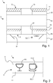
- Fig. 1 illustrates a cross-section of a user interface arrangement 1 according to some embodiments.
- the user interface arrangement 1 comprises a printed circuit board 3 having a first surface 5 and a second surface 7, and a light emitting unit 9.1, 9.2.
- the printed circuit board 3 comprises a first non-conductive layer 11 provided with at least one aperture 13.
- the light emitting unit 9.1, 9.2 is arranged to emit light through the at least one aperture 13 of the first non-conductive layer 11 in a direction from the second surface 7 to the first surface 5 of the printed circuit board 3 to thereby define an image visible at the first surface 5 of the printed circuit board 3. Since the image is visualized on the first surface 5 of the printed circuit board 3, the first surface 5 of the printed circuit board 3 defines the user interface of the user interface arrangement 1.
- the user interface arrangement 1 may be a user interface arrangement for an electric apparatus such as a display panel or a back-lit touch button display which can be configured to display text, numbers and/or symbols to a user.
- Such display of text, numbers and/or symbols can be used to indicate a state of an apparatus comprising such an arrangement and/or may be used to indicate a position and/or function of a touch button.
- the light emitting unit 9.1, 9.2 may comprise a light bulb or a Light Emitting Diode (LED). As illustrated in Fig. 1 , the light emitting unit 9.2 may be arranged on the printed circuit board 3. Since the user interface arrangement 1 comprises a printed circuit board 3, the light emitting unit 9.2 can easily be mounted onto the printed circuit board 3 and the wiring to such a light emitting unit 9.2 can easily be provided at a low cost.
- LED Light Emitting Diode
- the user interface arrangement 1 may further comprise a screen 27.
- the screen 27 may define an enclosure 29 enclosing the light emitting unit 9.1, 9.2.
- the screen 27 may comprise an inner surface 31 provided with a reflective surface arranged to reflect light emitted by the light emitting unit 9.1, 9.2.
- the light emitting unit 9.2 is arranged on the printed circuit board 3
- the light emitting unit 9.2 is arranged to emit light towards the inner surface 31 of the screen 27 such that light is reflected towards the at least one aperture 13 of the first non-conductive layer 11.
- the reflective surface may comprise paint in a bright colour or a metallic coating.
- the screen 27 may be formed by fiberglass.
- the first non-conductive layer 11 is provided on the first surface 5 of the printed circuit board 3.
- quality of the graphics of the image defined at the first surface 5 of the printed circuit board 3 may be improved.
- the first non-conductive layer 11 is a solder mask layer.
- a solder mask layer is a layer normally being used to reduce the risk of solder bridging while soldering components onto a printed circuit board. Applying a solder mask layer onto a printed circuit board is a well-known procedure and high volume manufacturing techniques have been developed for the purpose. Therefore, in embodiments wherein the first non-conductive layer 11 is a solder mask layer, high volume manufacturing techniques can be used in the manufacturing of the user interface arrangement 1. As a result, manufacturing costs of the user interface arrangement 1 is reduced.
- the printed circuit board 3 may further comprise a light diffuser layer 19.
- the light diffuser layer 19 is provided in a transparent or semi-transparent material.
- Such transparent or semi-transparent material may comprise fiberglass.
- the printed circuit board 3 further comprises a second non-conductive layer 17 where the light diffuser layer 19 is arranged between the first non-conductive layer 11 and the second non-conductive layer 17.
- the second non-conductive layer 11 is also be a solder mask layer.
- Such a second non-conductive layer 17 is also provided with at least one aperture 21 arranged substantially in a position corresponding to a position of the at least one aperture 13 of the first non-conductive layer 11 on the printed circuit board 3.
- a solder mask layer is applied to one or more free ends of the light diffuser layer 19 to thereby block light from passing such one or more of free ends of the light diffuser layer 19. Thereby, light is prevented from entering or exiting such one or more of free ends of the light diffuser layer 19.
- the light diffuser layer 19 may be arranged such that it changes the colour of light being emitted by the light emitting unit 9.1, 9.2. Further, by choosing a thickness of the light diffuser layer 19, an intensity of the light defining the image visible at the first surface can be varied.
- the size and the shape of the at least one aperture 21 of the second non-conductive layer 17 may substantially corresponds to the size and shape of the at least one aperture 13 of the first non-conductive layer 11.
- Fig. 2 illustrates the user interface arrangement 1 illustrated in Fig. 1 with the first surface 5 facing towards a viewer of the figure.
- the at least one aperture 13 of the first non-conductive layer 11 on the printed circuit board 3 is provided in the form of a wine glass symbol. Such a wine glass symbol may indicate the presence of a touch button with the function of starting a light wash of dishes.
- the size and the shape of the at least one aperture of the second non-conductive layer substantially corresponds to the size and shape of the at least one aperture 13 of the first non-conductive layer 11.
- such size and shape would substantially correspond to the size and shape of the wine glass symbol provided by the at least one aperture 13 of the first non-conductive layer 11.
- the size and the shape of the at least one aperture 21 of the second non-conductive layer 17 may be slightly larger than the size and shape of the at least one aperture 13 of the first non-conductive layer 11. Thereby, more light is emitted through the at least one aperture 21 of the second non-conductive layer 17 than the at least one aperture 13 of the first non-conductive layer 11. As a result, quality of the graphics of the image visible at the first surface 5 can be improved.
- buttons to the left showing a wine glass symbol and a button to the right showing a coffee cup symbol.
- the coffee cup symbol is provided by the first non-conductive layer 11 comprising two apertures 13.1, 13.2 which together form the coffee cup symbol.
- Such a coffee cup symbol may indicate the presence of a touch button with the function of starting a medium wash of dishes.
- a user interface arrangement 1 comprising a printed circuit board 3 comprising a first non-conductive layer 11 provided with at least one aperture 13, 13.1, 13.2 and where an image is defined by a light emitting unit 9.1, 9.2 being arranged to emit light through the at least one aperture 13, 13.1, 13.2, a variety of conceivable symbols or images can be provided, simply by arranging one or more apertures in the first non-conductive layer 11 in a particular shape or pattern.
- a user interface arrangement 1 can be provided comprising a first non-conductive layer 11 provided with seven apertures together forming a seven-segment display.
- Such a user interface arrangement may comprise seven light emitting units, one for each aperture.
- a user interface arrangement is provided capable of displaying numbers between 0-9.
- a user interface arrangement 1 can be provided comprising a first non-conductive layer 11 provided with a plurality of apertures each being provided with a light emitting unit, such that a user interface arrangement is provided capable of displaying commonly used letters or symbols.
- the two adjacent buttons illustrated in Fig. 2 may each comprise a light emitting unit (not shown).
- a light emitting unit When one of the two buttons is illuminated by a light emitting unit, some light may propagate through the light diffuser layer to the adjacent button. This phenomenon can be called over shine.
- the printed circuit board 3 may further comprise a touch sensing electrode layer 15 configured to detect presence of a touch event.
- the touch sensing electrode layer 15 may be a capacitor type sensing electrode layer 15.
- the touch sensing electrode layer 15 may comprise a copper layer.
- the printed circuit board 3 comprises two or more touch sensing electrode layers. Since the user interface arrangement comprises a printed circuit board 3, a touch sensing electrode layer 15 can be implemented in an easy manner at a low cost. Also, as illustrated in Fig. 1 , the touch sensing electrode layer 15 may be provided between the light diffuser layer 19 and the second non-conductive layer 17. Studies have shown that such a placement of the touch sensing electrode layer 15 have less impact on quality of the graphics of the image visible at the first surface 5 than placements closer to the first non-conductive layer 11.
- the user interface arrangement 1 may further comprise one or more processing units and may comprise one or more memory units connected thereto. Such one or more processing units may be configured to selectively turn on or off one or more light emitting units comprised in the arrangement 1. Also, such one or more processing units may be connected to the touch sensing electrode layer 15 to thereby detect presence of a touch event. Since the user interface arrangement 1 comprises a printed circuit board 3, implementation of such one or more processing units, one or more memory units and required wiring can be implemented in a simple manner at a low cost.
- the printed circuit board 3 may further comprise a ground plate layer 23. Electrical noise may cause issue with the detection of a touch event. In embodiments wherein the printed circuit board 3 further a ground plate layer 23, such electrical noise can be reduced. As a result, detection of the presence of a touch event can be improved.
- Fig. 2 two adjacent buttons are illustrated, a button to the left showing a wine glass symbol and a button to the right showing a coffee cup.
- the printed circuit board 3 comprises a ground plate layer 23
- such a ground plate layer 23 may facilitate detection of a touch event with the touch sensing electrode layer 15.
- one or more processing units connected to the touch sensing electrode layer 15 may more easily detect a position of a touch event on the user interface arrangement 1 such that the risk of an erroneous detection of a touch event is reduced.
- the second surface 7 of the printed circuit board 3 may comprise a reflective layer 25.
- a reflective layer 25 may reduce the amount of light the first and/or second non-conductive layer 11, 17 is subjected to. Thereby, a thickness of the first and/or second non-conductive layer 11, 17 can be reduced with unaffected quality of the graphics of the image defined at the first surface 5.
- light being emitted by the light emitting unit 9.1, 9.2 can be emitted to a surface of another component, e.g. an inner surface 31 of a screen 27, where it can be reflected in a direction towards the at least one aperture 13 of the first non-conductive layer 11 to thereby define an image visible at the first surface 5 of the printed circuit board 3.
- quality of the graphics of the image defined at the first surface 5 can be improved and a power of the light emitting unit 9.1, 9.2 can be reduced.
- the reflective layer 25 may be a silk screen layer.
- a silk screen layer may be provided in a bright colour, for example in the colour white.
- Applying a silk screen layer onto a printed circuit board is a commonly known procedure and high volume manufacturing techniques have been developed for the purpose. Therefore, in embodiments wherein the second surface 7 of the printed circuit board 3 comprises a reflective layer 25 in the form of a silk screen layer, high volume manufacturing techniques can be used in the manufacturing of the user interface arrangement 1. As a result, manufacturing costs of the user interface arrangement 1 can be reduced.
- Each one of the touch sensing electrode layer 15, the ground plate layer 23, and the reflective layer 25 is provided with at least one aperture arranged substantially in a position corresponding to a position of the at least one aperture 13 of the first non-conductive layer 11 on the printed circuit board 3.
- the size and the shape of such a at least one aperture of the touch sensing electrode layer 15, the ground plate layer 23, and the reflective layer 25 can at least substantially correspond to the size and shape of the at least one aperture 13 of the first non-conductive layer 11.
- the at least one aperture of the touch sensing electrode layer 15, the ground plate layer 23, and the reflective layer 25 are arranged such that light that is emitted in a straight angle towards the second surface 7 is emitted through the at least one aperture 13 of the first non-conducting layer 11 without being disturbed by the touch sensing electrode layer 15, the ground plate layer 23, and the reflective layer 25.
- the at least one aperture of one or more of the touch sensing electrode layer 15, the ground plate layer 23, and/or the reflective layer 2 may be made considerable larger than the at least one aperture 13 of the first non-conductive layer 11.
- Fig. 3 illustrates an electric apparatus 33 comprising a user interface arrangement 1 according to some embodiments.
- an electric apparatus 33 may be a house hold appliance.
- the electric apparatus 33 illustrated in Fig. 3 is a dishwasher.
- an electric apparatus 33 comprising a user interface arrangement 1 may be an electric household apparatus such as a vacuum cleaner, a coffee machine, a smoothing iron, a food processor, a food mixer, a hand blender, or the like.
- an electric apparatus 33 comprising a user interface arrangement 1 may be an oven, a microwave oven, a stove, a washing machine, a tumble dryer, a refrigerator, a heat pump apparatus, a kitchen fan or the like.
- Fig. 4 illustrates a method 100 for visualizing an image on a user interface arrangement, the method 100 comprising the steps of;
Landscapes
- Engineering & Computer Science (AREA)
- Microelectronics & Electronic Packaging (AREA)
- General Engineering & Computer Science (AREA)
- Structure Of Printed Boards (AREA)
- Push-Button Switches (AREA)
- Switches That Are Operated By Magnetic Or Electric Fields (AREA)
Claims (9)
- Benutzerschnittstellenanordnung (1), die Folgendes umfasst;- eine Leiterplatte (3) mit einer ersten Fläche (5) und einer zweiten Fläche (7) und- eine lichtemittierende Einheit (9.1, 9.2),wobei die Leiterplatte (3) eine erste nicht leitfähige Schicht (11) umfasst, die mit mindestens einer Öffnung (13) versehen ist, und wobei die lichtemittierende Einheit (9.1, 9.2) angeordnet ist, in eine Richtung von der zweiten Fläche (7) zur ersten Fläche (5) der Leiterplatte (3) Licht durch die mindestens eine Öffnung (13) der nicht leitfähigen Schicht (11) zu emittieren, um dadurch ein Bild zu definieren, das auf der ersten Fläche (5) der Leiterplatte (3) sichtbar ist, wobei die Leiterplatte (3) ferner eine zweite Schicht (17) und eine Lichtdiffusorschicht (19), die zwischen der ersten nicht leitfähigen Schicht (11) und der zweiten Schicht (17) angeordnet ist, umfasst und wobei die zweite Schicht (17) mit mindestens einer Öffnung (21) versehen ist, die im Wesentlichen in einer Position angeordnet ist, die einer Position der mindestens einen Öffnung (13) der ersten nicht leitfähigen Schicht (11) auf der Leiterplatte (3) entspricht, um via die mindestens eine Öffnung (21) der zweiten Schicht (17) und die mindestens eine Öffnung (13) der ersten nicht leitfähigen Schicht (11) Licht, das durch die Leiterplatte (3) in eine Richtung von der zweiten Fläche (7) zur ersten Fläche (5) der Leiterplatte (3) emittiert wird, aufzunehmen,
wobei die Größe und die Form der mindestens einen Öffnung (21) der zweiten Schicht (17) im Wesentlichen der Größe und der Form der mindestens einen Öffnung (13) der ersten nicht leitfähigen Schicht (11) entspricht,
wobei die erste nicht leitfähige Schicht (11) eine Lötmaskenschicht ist, wobei die erste nicht leitfähige Schicht (11) auf der ersten Fläche (5) der Leiterplatte (3) bereitgestellt ist und die zweite Schicht (17) auf der zweiten Fläche (7) der Leiterplatte (3) bereitgestellt ist, dadurch gekennzeichnet, dass die zweite Schicht eine zweite nicht leitfähige Schicht ist, und dadurch, dass die zweite nicht leitfähige Schicht (17) eine Lötmaskenschicht ist. - Benutzerschnittstellenanordnung (1) nach einem der vorhergehenden Ansprüche, wobei die Leiterplatte (3) ferner eine Berührungserfassungselektrodenschicht (15) umfasst, die dazu ausgelegt ist, das Vorhandensein eines Berührungsereignisses zu detektieren.
- Benutzerschnittstellenanordnung (1) nach Anspruch 2, wobei die Leiterplatte (3) ferner eine Erdungsplattenschicht (23) umfasst.
- Benutzerschnittstellenanordnung (1) nach einem der vorhergehenden Ansprüche, wobei die zweite Fläche (7) der Leiterplatte eine Reflexionsschicht (25) umfasst.
- Benutzerschnittstellenanordnung (1) nach Anspruch 4, wobei die Reflexionsschicht (25) eine Siebdruckschicht ist.
- Elektrische Vorrichtung (33), dadurch gekennzeichnet, dass die elektrische Vorrichtung (33) eine Benutzerschnittstellenanordnung (1) nach einem der vorhergehenden Ansprüche umfasst.
- Elektrische Vorrichtung (33) nach Anspruch 6, dadurch gekennzeichnet, dass die elektrische Vorrichtung (33) ein Geschirrspüler ist.
- Verwendung einer Leiterplatte (3) nach einem der vorhergehenden Ansprüche, um eine Benutzerschnittstellenanordnung (1) bereitzustellen.
- Verfahren (100) zum Visualisieren eines Bildes auf einer Benutzerschnittstellenanordnung (1), wobei das Verfahren (100) die folgenden Schritte umfasst;- Bereitstellen (101) einer Benutzerschnittstellenanordnung (1), wobei die Benutzerschnittstellenanordnung (1) eine Leiterplatte (3) mit einer ersten Fläche (5) und einer zweiten Fläche (7) und eine lichtemittierende Einheit (9.1, 9.2) umfasst, wobei die Leiterplatte (3) eine erste nicht leitfähige Schicht (11), die mit mindestens einer Öffnung (13) versehen ist, und eine zweite Schicht (17), die mit mindestens einer Öffnung (21), versehen ist, und eine Lichtdiffusorschicht (19), die zwischen der ersten nicht leitfähigen Schicht (11) und der zweiten Schicht (17) angeordnet ist, umfasst,
wobei die Größe und die Form der mindestens einen Öffnung (21) der zweiten Schicht (17) im Wesentlichen der Größe und der Form der Öffnung (13) der ersten nicht leitfähigen Schicht (11) entspricht und wobei die erste nicht leitfähige Schicht (11) eine Lötmaskenschicht ist,
wobei die erste nicht leitfähige Schicht (11) auf der ersten Fläche (5) der Leiterplatte (3) bereitgestellt ist und die zweite Schicht (17) auf der zweiten Fläche (7) der Leiterplatte (3) bereitgestellt ist; und- Emittieren (102) von Licht durch die mindestens eine Öffnung (13) der ersten nicht leitfähigen Schicht (11) in eine Richtung von der zweiten Fläche (7) zur ersten Fläche (5) der Leiterplatte (3), wodurch auf der ersten Fläche (5) der Leiterplatte (3) ein Bild visualisiert wird, dadurch gekennzeichnet, dass die zweite Schicht eine nicht leitfähige Schicht ist, und wobei die zweite nicht leitfähige Schicht (17) eine Lötmaskenschicht ist.
Priority Applications (1)
| Application Number | Priority Date | Filing Date | Title |
|---|---|---|---|
| PL13811878T PL3084963T3 (pl) | 2013-12-17 | 2013-12-17 | Układ interfejsu użytkownika |
Applications Claiming Priority (1)
| Application Number | Priority Date | Filing Date | Title |
|---|---|---|---|
| PCT/EP2013/076795 WO2015090361A1 (en) | 2013-12-17 | 2013-12-17 | User interface arrangement |
Publications (2)
| Publication Number | Publication Date |
|---|---|
| EP3084963A1 EP3084963A1 (de) | 2016-10-26 |
| EP3084963B1 true EP3084963B1 (de) | 2019-05-15 |
Family
ID=49880730
Family Applications (1)
| Application Number | Title | Priority Date | Filing Date |
|---|---|---|---|
| EP13811878.1A Active EP3084963B1 (de) | 2013-12-17 | 2013-12-17 | Benutzerschnittstellenanordnung |
Country Status (4)
| Country | Link |
|---|---|
| US (1) | US10051726B2 (de) |
| EP (1) | EP3084963B1 (de) |
| PL (1) | PL3084963T3 (de) |
| WO (1) | WO2015090361A1 (de) |
Families Citing this family (6)
| Publication number | Priority date | Publication date | Assignee | Title |
|---|---|---|---|---|
| DE102016212995A1 (de) * | 2016-07-15 | 2018-01-18 | BSH Hausgeräte GmbH | Bedienmodul für ein Haushaltsgerät |
| US10952315B2 (en) | 2019-07-29 | 2021-03-16 | Haier Us Appliance Solutions, Inc. | Light blocking features for indicator lights in an appliance |
| US10753597B1 (en) | 2019-07-29 | 2020-08-25 | Haier Us Appliance Solutions, Inc. | Light blocking features for indicator lights in an appliance |
| CN111625135A (zh) * | 2020-05-18 | 2020-09-04 | 卓力电器集团有限公司 | 一种电熨斗、电熨斗触摸控制方法及系统 |
| DE102020207158A1 (de) * | 2020-06-08 | 2021-12-09 | BSH Hausgeräte GmbH | Bedieneinheit für ein Haushaltsgerät |
| DE102020215166A1 (de) * | 2020-12-02 | 2022-06-02 | BSH Hausgeräte GmbH | Bedieneinheit für ein Haushaltsgerät |
Family Cites Families (31)
| Publication number | Priority date | Publication date | Assignee | Title |
|---|---|---|---|---|
| FR2352359A1 (fr) | 1976-05-17 | 1977-12-16 | Int Vibration Engineer | Panneau lumineux |
| US5239152A (en) | 1990-10-30 | 1993-08-24 | Donnelly Corporation | Touch sensor panel with hidden graphic mode |
| US5226723A (en) | 1992-05-11 | 1993-07-13 | Chen Der Jong | Light emitting diode display |
| US5397867A (en) * | 1992-09-04 | 1995-03-14 | Lucas Industries, Inc. | Light distribution for illuminated keyboard switches and displays |
| JPH0715406A (ja) | 1993-06-28 | 1995-01-17 | Nec Corp | 回路故障検出装置 |
| US5594222A (en) | 1994-10-25 | 1997-01-14 | Integrated Controls | Touch sensor and control circuit therefor |
| US5801345A (en) | 1996-06-21 | 1998-09-01 | Acuson Corporation | Keyboard assembly incorporating multiple lighting modes for improved user feedback |
| DE19649889C1 (de) | 1996-12-02 | 1997-10-30 | Kostal Leopold Gmbh & Co Kg | Elektrische Schaltvorrichtung |
| US6320282B1 (en) | 1999-01-19 | 2001-11-20 | Touchsensor Technologies, Llc | Touch switch with integral control circuit |
| DE19956542A1 (de) | 1999-11-24 | 2001-05-31 | Mannesmann Vdo Ag | Anzeigeinstrument, insbesondere in einem Kraftfahrzeug |
| US6608617B2 (en) | 2000-05-09 | 2003-08-19 | Marc O. Hoffknecht | Lighting control interface |
| FR2838558B1 (fr) | 2002-04-16 | 2005-10-14 | Faurecia Ind | Organe de commande de type capacitif |
| US7175304B2 (en) | 2003-01-30 | 2007-02-13 | Touchsensor Technologies, Llc | Integrated low profile display |
| US7850339B2 (en) | 2003-01-30 | 2010-12-14 | Touchsensor Technologies, Llc | Display having thin cross-section and/or multi-colored output |
| US20050134485A1 (en) | 2003-12-22 | 2005-06-23 | Hein David A. | Touch pad for motor vehicle and sensor therewith |
| EP1696404A1 (de) * | 2005-02-25 | 2006-08-30 | Electrovac, Fabrikation elektrotechnischer Spezialartikel Gesellschaft m.b.H. | Leuchtdiodenanordnung |
| DE102006022965A1 (de) | 2006-05-12 | 2007-11-15 | E.G.O. Elektro-Gerätebau GmbH | Bedieneinheit für Haushaltsgeräte |
| US20080090451A1 (en) | 2006-10-12 | 2008-04-17 | Sangoma Technologies Corporation | Apparatus and method for integrating an indicator light in a connector assembly |
| US7707257B2 (en) | 2007-06-27 | 2010-04-27 | International Business Machines Corporation | System and method for transforming a thread of email messages into a real-time meeting |
| EP2048781B1 (de) | 2007-10-08 | 2018-06-13 | Whirlpool Corporation | Berührungsschalter für Elektrogeräte und Elektrogerät mit derartigem Schalter |
| PL2048779T3 (pl) | 2007-10-08 | 2012-05-31 | Whirlpool Co | Pojemnościowy przełącznik dotykowy i urządzenie gospodarstwa domowego wyposażone w taki przełącznik |
| CN201129642Y (zh) | 2007-11-29 | 2008-10-08 | 博西华电器(江苏)有限公司 | 发光二极管显示模组以及使用该模组的洗涤设备 |
| US7825345B1 (en) | 2008-08-26 | 2010-11-02 | Kano Yoshio W | Reversely mounted tactile switch assembly and printed circuit board therewith |
| US8408723B2 (en) * | 2009-09-01 | 2013-04-02 | Microchip Technology Incorporated | Backlighting inductive touch buttons |
| US8092061B2 (en) | 2009-04-15 | 2012-01-10 | Delphi Technologies, Inc. | Pipe having light-redirecting channels |
| US8390481B2 (en) * | 2009-08-17 | 2013-03-05 | Apple Inc. | Sensing capacitance changes of a housing of an electronic device |
| US9109774B1 (en) * | 2011-07-20 | 2015-08-18 | Cooper Technologies Company | Systems, methods and devices for an LED lighting module with a light transmissive cover |
| US20130163272A1 (en) | 2011-12-23 | 2013-06-27 | Touchsensor Technologies, Llc | User interface lighting apparatus |
| US8807770B2 (en) | 2012-01-30 | 2014-08-19 | General Electric Company | Appliance user interface having reverse mount LEDs |
| EP2662981A1 (de) | 2012-05-07 | 2013-11-13 | Diehl AKO Stiftung & Co. KG | Kapazitiver Näherungs- und/oder Kontaktschalter mit schwimmender Elektrode |
| US8827477B2 (en) | 2012-12-12 | 2014-09-09 | General Electric Company | Refrigerator appliance |
-
2013
- 2013-12-17 US US15/036,177 patent/US10051726B2/en active Active
- 2013-12-17 WO PCT/EP2013/076795 patent/WO2015090361A1/en not_active Ceased
- 2013-12-17 PL PL13811878T patent/PL3084963T3/pl unknown
- 2013-12-17 EP EP13811878.1A patent/EP3084963B1/de active Active
Non-Patent Citations (1)
| Title |
|---|
| None * |
Also Published As
| Publication number | Publication date |
|---|---|
| WO2015090361A1 (en) | 2015-06-25 |
| US20160295688A1 (en) | 2016-10-06 |
| US10051726B2 (en) | 2018-08-14 |
| PL3084963T3 (pl) | 2019-11-29 |
| EP3084963A1 (de) | 2016-10-26 |
Similar Documents
| Publication | Publication Date | Title |
|---|---|---|
| EP3084963B1 (de) | Benutzerschnittstellenanordnung | |
| US10581430B2 (en) | Backlighting appliance deadfronted user interfaces | |
| US9235306B2 (en) | Operating and display device for a domestic appliance, and domestic appliance | |
| EP2048779B1 (de) | Kapazitiver Berührungsschalter und Haushaltsgerät mit diesem | |
| US8310839B2 (en) | Capacitive touch switch and domestic appliance provided with such switch | |
| US9954525B2 (en) | Touch- and/or proximity-sensitive input device, and household appliance having the input device | |
| US9973190B2 (en) | Capacitive proximity and/or contact switch | |
| RU2591144C2 (ru) | Бытовой прибор с сенсорным устройством управления и индикации | |
| EP3779636A1 (de) | Berührungsfenster für berührungssensor und haushaltsgerät damit | |
| CN109989226A (zh) | 具有照明面的家用大型器具 | |
| EP4535137A1 (de) | Berührungsfeldstruktur zur anzeige von mustern | |
| CN104185437A (zh) | 用于家用器具的显示控制元件 | |
| US11162203B2 (en) | Appliance control module with in-molded electronics | |
| CN105874276B (zh) | 家用电器操作装置 | |
| US20150113841A1 (en) | Alphanumeric display assembly | |
| US20180248547A1 (en) | Capacitive touch switch, configuration of capacitive touch switches and operating device | |
| CN110383692A (zh) | 具有屏蔽电磁干扰的电容式触摸屏的家用器具和用于制造其的方法 | |
| CN105452555B (zh) | 在模制基板上并且具有非齐平反向安装led的印刷电容式触摸屏 | |
| KR20150069385A (ko) | 가전기기 | |
| US11330722B2 (en) | Appliance control panel with in-molded electronic film directly mounted to printed circuit board | |
| CN217506793U (zh) | 显示装置及家用电器 | |
| CN120071775A (zh) | 显示模块、显示装置和电器 | |
| KR20130016357A (ko) | 가전기기용 장치 |
Legal Events
| Date | Code | Title | Description |
|---|---|---|---|
| PUAI | Public reference made under article 153(3) epc to a published international application that has entered the european phase |
Free format text: ORIGINAL CODE: 0009012 |
|
| 17P | Request for examination filed |
Effective date: 20160718 |
|
| AK | Designated contracting states |
Kind code of ref document: A1 Designated state(s): AL AT BE BG CH CY CZ DE DK EE ES FI FR GB GR HR HU IE IS IT LI LT LU LV MC MK MT NL NO PL PT RO RS SE SI SK SM TR |
|
| AX | Request for extension of the european patent |
Extension state: BA ME |
|
| DAX | Request for extension of the european patent (deleted) | ||
| STAA | Information on the status of an ep patent application or granted ep patent |
Free format text: STATUS: EXAMINATION IS IN PROGRESS |
|
| 17Q | First examination report despatched |
Effective date: 20180712 |
|
| GRAJ | Information related to disapproval of communication of intention to grant by the applicant or resumption of examination proceedings by the epo deleted |
Free format text: ORIGINAL CODE: EPIDOSDIGR1 |
|
| STAA | Information on the status of an ep patent application or granted ep patent |
Free format text: STATUS: GRANT OF PATENT IS INTENDED |
|
| GRAP | Despatch of communication of intention to grant a patent |
Free format text: ORIGINAL CODE: EPIDOSNIGR1 |
|
| INTG | Intention to grant announced |
Effective date: 20181206 |
|
| RIN1 | Information on inventor provided before grant (corrected) |
Inventor name: GUSTAFSSON, AGNE |
|
| GRAS | Grant fee paid |
Free format text: ORIGINAL CODE: EPIDOSNIGR3 |
|
| GRAA | (expected) grant |
Free format text: ORIGINAL CODE: 0009210 |
|
| STAA | Information on the status of an ep patent application or granted ep patent |
Free format text: STATUS: THE PATENT HAS BEEN GRANTED |
|
| AK | Designated contracting states |
Kind code of ref document: B1 Designated state(s): AL AT BE BG CH CY CZ DE DK EE ES FI FR GB GR HR HU IE IS IT LI LT LU LV MC MK MT NL NO PL PT RO RS SE SI SK SM TR |
|
| REG | Reference to a national code |
Ref country code: CH Ref legal event code: EP |
|
| REG | Reference to a national code |
Ref country code: DE Ref legal event code: R096 Ref document number: 602013055505 Country of ref document: DE |
|
| REG | Reference to a national code |
Ref country code: IE Ref legal event code: FG4D |
|
| REG | Reference to a national code |
Ref country code: NL Ref legal event code: MP Effective date: 20190515 |
|
| REG | Reference to a national code |
Ref country code: LT Ref legal event code: MG4D |
|
| PG25 | Lapsed in a contracting state [announced via postgrant information from national office to epo] |
Ref country code: FI Free format text: LAPSE BECAUSE OF FAILURE TO SUBMIT A TRANSLATION OF THE DESCRIPTION OR TO PAY THE FEE WITHIN THE PRESCRIBED TIME-LIMIT Effective date: 20190515 Ref country code: NO Free format text: LAPSE BECAUSE OF FAILURE TO SUBMIT A TRANSLATION OF THE DESCRIPTION OR TO PAY THE FEE WITHIN THE PRESCRIBED TIME-LIMIT Effective date: 20190815 Ref country code: LT Free format text: LAPSE BECAUSE OF FAILURE TO SUBMIT A TRANSLATION OF THE DESCRIPTION OR TO PAY THE FEE WITHIN THE PRESCRIBED TIME-LIMIT Effective date: 20190515 Ref country code: NL Free format text: LAPSE BECAUSE OF FAILURE TO SUBMIT A TRANSLATION OF THE DESCRIPTION OR TO PAY THE FEE WITHIN THE PRESCRIBED TIME-LIMIT Effective date: 20190515 Ref country code: ES Free format text: LAPSE BECAUSE OF FAILURE TO SUBMIT A TRANSLATION OF THE DESCRIPTION OR TO PAY THE FEE WITHIN THE PRESCRIBED TIME-LIMIT Effective date: 20190515 Ref country code: HR Free format text: LAPSE BECAUSE OF FAILURE TO SUBMIT A TRANSLATION OF THE DESCRIPTION OR TO PAY THE FEE WITHIN THE PRESCRIBED TIME-LIMIT Effective date: 20190515 Ref country code: AL Free format text: LAPSE BECAUSE OF FAILURE TO SUBMIT A TRANSLATION OF THE DESCRIPTION OR TO PAY THE FEE WITHIN THE PRESCRIBED TIME-LIMIT Effective date: 20190515 Ref country code: SE Free format text: LAPSE BECAUSE OF FAILURE TO SUBMIT A TRANSLATION OF THE DESCRIPTION OR TO PAY THE FEE WITHIN THE PRESCRIBED TIME-LIMIT Effective date: 20190515 Ref country code: PT Free format text: LAPSE BECAUSE OF FAILURE TO SUBMIT A TRANSLATION OF THE DESCRIPTION OR TO PAY THE FEE WITHIN THE PRESCRIBED TIME-LIMIT Effective date: 20190915 |
|
| PG25 | Lapsed in a contracting state [announced via postgrant information from national office to epo] |
Ref country code: LV Free format text: LAPSE BECAUSE OF FAILURE TO SUBMIT A TRANSLATION OF THE DESCRIPTION OR TO PAY THE FEE WITHIN THE PRESCRIBED TIME-LIMIT Effective date: 20190515 Ref country code: GR Free format text: LAPSE BECAUSE OF FAILURE TO SUBMIT A TRANSLATION OF THE DESCRIPTION OR TO PAY THE FEE WITHIN THE PRESCRIBED TIME-LIMIT Effective date: 20190816 Ref country code: RS Free format text: LAPSE BECAUSE OF FAILURE TO SUBMIT A TRANSLATION OF THE DESCRIPTION OR TO PAY THE FEE WITHIN THE PRESCRIBED TIME-LIMIT Effective date: 20190515 Ref country code: BG Free format text: LAPSE BECAUSE OF FAILURE TO SUBMIT A TRANSLATION OF THE DESCRIPTION OR TO PAY THE FEE WITHIN THE PRESCRIBED TIME-LIMIT Effective date: 20190815 |
|
| REG | Reference to a national code |
Ref country code: AT Ref legal event code: MK05 Ref document number: 1134621 Country of ref document: AT Kind code of ref document: T Effective date: 20190515 |
|
| PG25 | Lapsed in a contracting state [announced via postgrant information from national office to epo] |
Ref country code: RO Free format text: LAPSE BECAUSE OF FAILURE TO SUBMIT A TRANSLATION OF THE DESCRIPTION OR TO PAY THE FEE WITHIN THE PRESCRIBED TIME-LIMIT Effective date: 20190515 Ref country code: CZ Free format text: LAPSE BECAUSE OF FAILURE TO SUBMIT A TRANSLATION OF THE DESCRIPTION OR TO PAY THE FEE WITHIN THE PRESCRIBED TIME-LIMIT Effective date: 20190515 Ref country code: SK Free format text: LAPSE BECAUSE OF FAILURE TO SUBMIT A TRANSLATION OF THE DESCRIPTION OR TO PAY THE FEE WITHIN THE PRESCRIBED TIME-LIMIT Effective date: 20190515 Ref country code: AT Free format text: LAPSE BECAUSE OF FAILURE TO SUBMIT A TRANSLATION OF THE DESCRIPTION OR TO PAY THE FEE WITHIN THE PRESCRIBED TIME-LIMIT Effective date: 20190515 Ref country code: EE Free format text: LAPSE BECAUSE OF FAILURE TO SUBMIT A TRANSLATION OF THE DESCRIPTION OR TO PAY THE FEE WITHIN THE PRESCRIBED TIME-LIMIT Effective date: 20190515 Ref country code: DK Free format text: LAPSE BECAUSE OF FAILURE TO SUBMIT A TRANSLATION OF THE DESCRIPTION OR TO PAY THE FEE WITHIN THE PRESCRIBED TIME-LIMIT Effective date: 20190515 |
|
| REG | Reference to a national code |
Ref country code: DE Ref legal event code: R097 Ref document number: 602013055505 Country of ref document: DE |
|
| PG25 | Lapsed in a contracting state [announced via postgrant information from national office to epo] |
Ref country code: SM Free format text: LAPSE BECAUSE OF FAILURE TO SUBMIT A TRANSLATION OF THE DESCRIPTION OR TO PAY THE FEE WITHIN THE PRESCRIBED TIME-LIMIT Effective date: 20190515 |
|
| PLBE | No opposition filed within time limit |
Free format text: ORIGINAL CODE: 0009261 |
|
| STAA | Information on the status of an ep patent application or granted ep patent |
Free format text: STATUS: NO OPPOSITION FILED WITHIN TIME LIMIT |
|
| 26N | No opposition filed |
Effective date: 20200218 |
|
| PG25 | Lapsed in a contracting state [announced via postgrant information from national office to epo] |
Ref country code: SI Free format text: LAPSE BECAUSE OF FAILURE TO SUBMIT A TRANSLATION OF THE DESCRIPTION OR TO PAY THE FEE WITHIN THE PRESCRIBED TIME-LIMIT Effective date: 20190515 |
|
| REG | Reference to a national code |
Ref country code: CH Ref legal event code: PL |
|
| REG | Reference to a national code |
Ref country code: BE Ref legal event code: MM Effective date: 20191231 |
|
| PG25 | Lapsed in a contracting state [announced via postgrant information from national office to epo] |
Ref country code: MC Free format text: LAPSE BECAUSE OF FAILURE TO SUBMIT A TRANSLATION OF THE DESCRIPTION OR TO PAY THE FEE WITHIN THE PRESCRIBED TIME-LIMIT Effective date: 20190515 |
|
| GBPC | Gb: european patent ceased through non-payment of renewal fee |
Effective date: 20191217 |
|
| PG25 | Lapsed in a contracting state [announced via postgrant information from national office to epo] |
Ref country code: LU Free format text: LAPSE BECAUSE OF NON-PAYMENT OF DUE FEES Effective date: 20191217 Ref country code: IE Free format text: LAPSE BECAUSE OF NON-PAYMENT OF DUE FEES Effective date: 20191217 Ref country code: FR Free format text: LAPSE BECAUSE OF NON-PAYMENT OF DUE FEES Effective date: 20191231 Ref country code: GB Free format text: LAPSE BECAUSE OF NON-PAYMENT OF DUE FEES Effective date: 20191217 |
|
| PG25 | Lapsed in a contracting state [announced via postgrant information from national office to epo] |
Ref country code: BE Free format text: LAPSE BECAUSE OF NON-PAYMENT OF DUE FEES Effective date: 20191231 Ref country code: LI Free format text: LAPSE BECAUSE OF NON-PAYMENT OF DUE FEES Effective date: 20191231 Ref country code: CH Free format text: LAPSE BECAUSE OF NON-PAYMENT OF DUE FEES Effective date: 20191231 |
|
| PG25 | Lapsed in a contracting state [announced via postgrant information from national office to epo] |
Ref country code: CY Free format text: LAPSE BECAUSE OF FAILURE TO SUBMIT A TRANSLATION OF THE DESCRIPTION OR TO PAY THE FEE WITHIN THE PRESCRIBED TIME-LIMIT Effective date: 20190515 |
|
| PG25 | Lapsed in a contracting state [announced via postgrant information from national office to epo] |
Ref country code: IS Free format text: LAPSE BECAUSE OF FAILURE TO SUBMIT A TRANSLATION OF THE DESCRIPTION OR TO PAY THE FEE WITHIN THE PRESCRIBED TIME-LIMIT Effective date: 20190915 |
|
| PG25 | Lapsed in a contracting state [announced via postgrant information from national office to epo] |
Ref country code: HU Free format text: LAPSE BECAUSE OF FAILURE TO SUBMIT A TRANSLATION OF THE DESCRIPTION OR TO PAY THE FEE WITHIN THE PRESCRIBED TIME-LIMIT; INVALID AB INITIO Effective date: 20131217 Ref country code: MT Free format text: LAPSE BECAUSE OF FAILURE TO SUBMIT A TRANSLATION OF THE DESCRIPTION OR TO PAY THE FEE WITHIN THE PRESCRIBED TIME-LIMIT Effective date: 20190515 |
|
| PG25 | Lapsed in a contracting state [announced via postgrant information from national office to epo] |
Ref country code: MK Free format text: LAPSE BECAUSE OF FAILURE TO SUBMIT A TRANSLATION OF THE DESCRIPTION OR TO PAY THE FEE WITHIN THE PRESCRIBED TIME-LIMIT Effective date: 20190515 |
|
| PGFP | Annual fee paid to national office [announced via postgrant information from national office to epo] |
Ref country code: DE Payment date: 20221213 Year of fee payment: 10 |
|
| PGFP | Annual fee paid to national office [announced via postgrant information from national office to epo] |
Ref country code: PL Payment date: 20221209 Year of fee payment: 10 |
|
| PGFP | Annual fee paid to national office [announced via postgrant information from national office to epo] |
Ref country code: TR Payment date: 20221215 Year of fee payment: 10 |
|
| PGFP | Annual fee paid to national office [announced via postgrant information from national office to epo] |
Ref country code: IT Payment date: 20221228 Year of fee payment: 10 |
|
| P01 | Opt-out of the competence of the unified patent court (upc) registered |
Effective date: 20230625 |
|
| REG | Reference to a national code |
Ref country code: DE Ref legal event code: R119 Ref document number: 602013055505 Country of ref document: DE |
|
| PG25 | Lapsed in a contracting state [announced via postgrant information from national office to epo] |
Ref country code: DE Free format text: LAPSE BECAUSE OF NON-PAYMENT OF DUE FEES Effective date: 20240702 |
|
| PG25 | Lapsed in a contracting state [announced via postgrant information from national office to epo] |
Ref country code: DE Free format text: LAPSE BECAUSE OF NON-PAYMENT OF DUE FEES Effective date: 20240702 |
|
| PG25 | Lapsed in a contracting state [announced via postgrant information from national office to epo] |
Ref country code: PL Free format text: LAPSE BECAUSE OF NON-PAYMENT OF DUE FEES Effective date: 20231217 |
|
| PG25 | Lapsed in a contracting state [announced via postgrant information from national office to epo] |
Ref country code: IT Free format text: LAPSE BECAUSE OF NON-PAYMENT OF DUE FEES Effective date: 20231217 |