EP3086368A2 - Elektronischer chip, der eine geschützte rückseite umfasst - Google Patents
Elektronischer chip, der eine geschützte rückseite umfasst Download PDFInfo
- Publication number
- EP3086368A2 EP3086368A2 EP16165837.2A EP16165837A EP3086368A2 EP 3086368 A2 EP3086368 A2 EP 3086368A2 EP 16165837 A EP16165837 A EP 16165837A EP 3086368 A2 EP3086368 A2 EP 3086368A2
- Authority
- EP
- European Patent Office
- Prior art keywords
- protective layer
- electronic chip
- resistive element
- electronic
- substrate
- Prior art date
- Legal status (The legal status is an assumption and is not a legal conclusion. Google has not performed a legal analysis and makes no representation as to the accuracy of the status listed.)
- Granted
Links
Images








Classifications
-
- H—ELECTRICITY
- H10—SEMICONDUCTOR DEVICES; ELECTRIC SOLID-STATE DEVICES NOT OTHERWISE PROVIDED FOR
- H10W—GENERIC PACKAGES, INTERCONNECTIONS, CONNECTORS OR OTHER CONSTRUCTIONAL DETAILS OF DEVICES COVERED BY CLASS H10
- H10W42/00—Arrangements for protection of devices
-
- H—ELECTRICITY
- H10—SEMICONDUCTOR DEVICES; ELECTRIC SOLID-STATE DEVICES NOT OTHERWISE PROVIDED FOR
- H10W—GENERIC PACKAGES, INTERCONNECTIONS, CONNECTORS OR OTHER CONSTRUCTIONAL DETAILS OF DEVICES COVERED BY CLASS H10
- H10W42/00—Arrangements for protection of devices
- H10W42/40—Arrangements for protection of devices protecting against tampering, e.g. unauthorised inspection or reverse engineering
-
- G—PHYSICS
- G09—EDUCATION; CRYPTOGRAPHY; DISPLAY; ADVERTISING; SEALS
- G09C—CIPHERING OR DECIPHERING APPARATUS FOR CRYPTOGRAPHIC OR OTHER PURPOSES INVOLVING THE NEED FOR SECRECY
- G09C1/00—Apparatus or methods whereby a given sequence of signs, e.g. an intelligible text, is transformed into an unintelligible sequence of signs by transposing the signs or groups of signs or by replacing them by others according to a predetermined system
-
- H—ELECTRICITY
- H04—ELECTRIC COMMUNICATION TECHNIQUE
- H04L—TRANSMISSION OF DIGITAL INFORMATION, e.g. TELEGRAPHIC COMMUNICATION
- H04L9/00—Cryptographic mechanisms or cryptographic arrangements for secret or secure communications; Network security protocols
- H04L9/002—Countermeasures against attacks on cryptographic mechanisms
- H04L9/003—Countermeasures against attacks on cryptographic mechanisms for power analysis, e.g. differential power analysis [DPA] or simple power analysis [SPA]
-
- H—ELECTRICITY
- H04—ELECTRIC COMMUNICATION TECHNIQUE
- H04L—TRANSMISSION OF DIGITAL INFORMATION, e.g. TELEGRAPHIC COMMUNICATION
- H04L9/00—Cryptographic mechanisms or cryptographic arrangements for secret or secure communications; Network security protocols
- H04L9/002—Countermeasures against attacks on cryptographic mechanisms
- H04L9/004—Countermeasures against attacks on cryptographic mechanisms for fault attacks
-
- H—ELECTRICITY
- H10—SEMICONDUCTOR DEVICES; ELECTRIC SOLID-STATE DEVICES NOT OTHERWISE PROVIDED FOR
- H10W—GENERIC PACKAGES, INTERCONNECTIONS, CONNECTORS OR OTHER CONSTRUCTIONAL DETAILS OF DEVICES COVERED BY CLASS H10
- H10W42/00—Arrangements for protection of devices
- H10W42/40—Arrangements for protection of devices protecting against tampering, e.g. unauthorised inspection or reverse engineering
- H10W42/405—Arrangements for protection of devices protecting against tampering, e.g. unauthorised inspection or reverse engineering using active circuits
-
- H—ELECTRICITY
- H10—SEMICONDUCTOR DEVICES; ELECTRIC SOLID-STATE DEVICES NOT OTHERWISE PROVIDED FOR
- H10W—GENERIC PACKAGES, INTERCONNECTIONS, CONNECTORS OR OTHER CONSTRUCTIONAL DETAILS OF DEVICES COVERED BY CLASS H10
- H10W74/00—Encapsulations, e.g. protective coatings
- H10W74/10—Encapsulations, e.g. protective coatings characterised by their shape or disposition
-
- H—ELECTRICITY
- H04—ELECTRIC COMMUNICATION TECHNIQUE
- H04L—TRANSMISSION OF DIGITAL INFORMATION, e.g. TELEGRAPHIC COMMUNICATION
- H04L2209/00—Additional information or applications relating to cryptographic mechanisms or cryptographic arrangements for secret or secure communication H04L9/00
- H04L2209/12—Details relating to cryptographic hardware or logic circuitry
Definitions
- the invention relates to the field of security and protection of electronic chips, and relates to an electronic chip comprising means protecting the rear face of the electronic chip and for preventing access to the electronic circuit of the chip since its back side.
- the invention applies to any type of electronic chip used in particular in a smart card: mobile phone chip, bank card, health card, identity document, etc.
- the attacks that can undergo an electronic chip are generally intended to access confidential data stored in the electronic circuit of the chip in order to clone, modify the stored information, impersonate its owner, etc.
- An electronic chip can be attacked in many ways: chemical, physical, laser, electromagnetic, electrical, etc.
- the front face of an electronic chip that is to say the face of the chip at which the electronic circuit is located, is generally protected by multiple means such as a protective layer protecting the chip against Focused ion probe intrusive attacks (FIB or "Focused Ion Beam”), as well as other protections against glitch, electromagnetic, or cryptanalysis, etc.
- FIB Focused ion probe intrusive attacks
- cryptanalysis etc.
- the back of the electronic chip is generally poorly protected. Without means of protection of this rear face, nothing prevents the implementation of a thinning of the substrate of the chip at its rear face, or the realization of electronic or electrical failures with the infrared laser ("glitch "),
- the silicon (which is the material generally used) of the substrate being transparent to the characteristic wavelengths of the infrared.
- the access to the electronic circuit of the chip obtained then makes it possible, for example, to read the data by obtaining the encryption key.
- the access to the secret information of the electronic chips is feasible not only by disturbances by laser stimulation but also by the realization of probing type contact pads directly connected inside the electronic circuit, and this thanks to the modification circuit physics by a focused ion probe (FIB beam).
- FIB beam focused ion probe
- the document DE 100 65 339 A1 describes the protection of a rear face of an electronic chip through the realization of several capacities at this rear face.
- an action such as faulting of the chip
- Such protection is however not suitable for protecting the chip against ion beam ablation attacks. Indeed, even with an optimized design, the sensitivity of the capacitors in the rear face is not sufficient because of their very large total surface, and an impairment of these capacities by ion beams is very difficult to detect.
- ion beam etching is carried out on an etching window of 50 ⁇ m on one side, ie an area equal to 2.5 ⁇ 10 -3 mm 2 . Considering a chip of standard size of area equal to 4 mm 2 , the etching window represents a variation of less than 1/1000 of the surface of the chip.
- the document US 8 110 894 B2 discloses an electronic chip whose front face comprises an inductor which, by inductive coupling through the chip substrate, detects the presence of a conductive ground plane disposed on the rear face of the chip. An alteration by an attack of this conductive ground plane induces a variation of the inductive coupling between the front and rear faces of the chip, which leads to faulting of the chip.
- An object of the present invention is to provide an electronic chip whose rear face is effectively protected vis-à-vis various types of attack, particularly against thinning attacks, by ion probe or by etching chemical from the back side of the chip.
- this thinning necessarily causes, after the destruction of the second protective layer, that of the resistive element. This destruction of the resistive element then forms an open circuit which is detected by the electronic circuit of the chip which may, for example, fail.
- the chemical etching agent used to etch the substrate for example a solution based on, or comprising, KOH and / or TMAH and / or hydrofluoric acid and / or nitric acid, also destroys the two protective layers, and in particular the first protective layer which mechanically supports the resistive element, due to the nature of the materials of these protective layers which also undergo the etching implemented to etch the substrate.
- This destruction of the protective layers therefore also causes destruction of the resistive element which is no longer mechanically supported by the first protective layer, this destruction being detected by the electronic circuit of the chip.
- the first protective layer is etched chemically even if the second protective layer is more difficult to attack by the etching agent used. Since the dielectric material of the first protective layer has an etching resistance lower than or equal to that of the dielectric material of the second protective layer, the first protective layer is etched more rapidly than the second protective layer (or the same speed when the two layers of protection are of the same nature), which implies that a detection of the intrusion or the attack occurs (via the destruction of the resistive element which is no longer mechanically supported) before the resistive element can be reached and modified by this etching from the second protective layer. In addition, the chemical etching of the first protective layer generally results in the removal of at least a portion of the second protective layer.
- the first protective layer may be thinner, or thinner, than the second protective layer.
- Resistance to chemical etching can be quantified by the rate of etching or etching or dissolution of the material in ⁇ m / min for an aqueous solution or a given chemistry corresponding to the chemical etching agent. This rate can be measured by measuring the thickness of a layer before and after exposure to the chemical etching agent for a specified period of time. The ratio of the thickness difference measured over time gives the attack speed.
- the dielectric material of the protective layers makes the focused ion probe attacks difficult. Indeed, when the dielectric material of the protective layers is subjected to an ion beam, these ions accumulate in the dielectric material at the location targeted by the beam, which creates a localized electric charge which causes a shift of the ion beam. Ablation of the material then becomes very difficult if not impossible because the ion beam deviates and fails to penetrate deeply into the dielectric material to reach the electronic circuit. In addition, even if a high energy ion beam is used to pass through the dielectric material of the protective layers, this ion beam then damages the resistive element, thus modifying its electrical resistance and thus triggering detection of this attack. by the electronic circuit of the chip.
- the invention therefore proposes an electronic chip comprising, on the rear face, a combination of an active protection structure (the resistive element) and a passive protection structure (the protective layers) while making this protection system totally opaque. vis-à-vis an attack of the back side of the chip.
- the part of the electronic circuit opposite which the resistive element is arranged may be any part of the electronic circuit, and in particular an electrical routing part, or an active zone comprising for example at least one transistor and / or at least one a memory.
- At least the dielectric material of the second protective layer may be resistant to mechanical polishing and / or opaque to infrared radiation and / or resistant to focused ion probe attack.
- an opaque dielectric material vis-à-vis infrared radiation forms an additional protection vis-à-vis attacks by infrared radiation, for example by infrared laser.
- infrared radiation for example means a material having a transmission coefficient of less than about 20% with respect to infrared radiation.
- resistant to a focused ion probe attack designates, for example, a material whose abrasion rate by the focused ion probe is less than about 0.5 ⁇ m / min for a 50 ⁇ 50 attack window. 2 .mu.m.
- At least the dielectric material of the second protective layer may have a Young's modulus greater than or equal to about 1 GPa. Such a Young's modulus gives good resistance to mechanical polishing or mechanical thinning.
- the dielectric material of the first protective layer and / or the dielectric material of the second protective layer may be a non-mineral material and / or a polymer and / or may comprise epoxy and / or may comprise silicone.
- the choice of such materials to achieve the protective layers is advantageous because they make it easy to achieve the protective layers on either side of the resistive element.
- the first protective layer and / or the second protective layer may further comprise particles of a first material different from the dielectric material of the first protective layer and / or the dielectric material of the second protective layer, and which are distributed throughout the dielectric material of the first protective layer and / or the dielectric material of the second protective layer.
- Such particles may in particular form additional protection against FIB etching of the protective layer or layers comprising these particles.
- This protection against FIB etching can be obtained thanks to the high hardness of the first material of the particles (by example of alumina having a Vickers hardness of the order of 1500 kgf.mm -2 ), this hardness being for example greater than or equal to 100 kgf.mm -2 .
- the first material may also be such that the particles disturb a laser beam used on the protective layer or layers which comprise these particles.
- Such particles may be added in the material of one of the protective layers or in the materials of the protective layers also when this or these materials are dielectric materials other than polymers.
- the first material of the particles may comprise or be based on silica and / or alumina.
- the first material of the particles may be covered with a second material reflective vis-à-vis light and / or electronic and / or ion, for example a metallic material.
- This reflective coating makes it possible to further disturb a light (for example laser) and / or an electronic and / or ionic (FIB) beam that would be applied to the dielectric material of the protective layers.
- These reflective particles are advantageously used for the second protective layer which has a free face forming the rear face of the electronic chip.
- the second material can be called reflective when it reflects at least 50% of the light and / or electronic and / or ion.
- the resistive element may comprise at least one conductive track having at least one serpentine pattern and / or several alternating patterns, intermingled, wound or interlaced.
- Such a configuration of the resistive element can make it difficult or even prevent the realization of a metal bridge or a short circuit between two parts of the resistive element ("bend wire") for the purpose of access to the part of the back face are between these two parts of the resistive element without changing the value of the electrical resistance of the resistive element.
- the pattern of the resistive element can cover the first protective layer as much as possible, and covers for example the entire portion of the first protective layer facing the part of the electronic circuit in front of which is located the resistive element to detect at best an attack on the rear face of the electronic chip.
- the conductive track may have a width of between approximately 5 ⁇ m and 50 ⁇ m, and / or portions of the conductive track which are adjacent and parallel to one another may be spaced apart from one another. another of a distance of between about 5 ⁇ m and 50 ⁇ m.
- the electronic chip may further comprise an electrically conductive layer disposed between the rear face of the substrate and the first protective layer.
- an electrically conductive layer forms an additional shielding vis-à-vis a laser beam and / or other electromagnetic radiation that can be used to attack the back side of the electronic chip.
- the rear face of the substrate may be electrically insulating or rendered electrically insulating by the prior deposition of an electrically insulating layer on this rear face.
- the electronic chip may further comprise at least two first conductive vias crossing the substrate and electrically connecting the resistive element to the electronic circuit.
- the electronic chip may further comprise an inductive element disposed at the front face of the substrate and electrically connected to the electronic circuit
- the resistive element may be part of an RLC circuit (ie an electrical circuit having an electrical resistance, an inductance and a capacitance) adapted to be inductively coupled to said inductive element such that a change in a value of inductance of the inductive element induces a modification of a property electrical circuit RLC.
- the resistive element is connected to the electronic circuit inductively without using conductive vias crossing the substrate.
- the inductive element can be integrated in the electronic circuit.
- the resistive element can form a coil whose ends are electrically connected to one another.
- the layer electrically conductive disposed between the rear face of the substrate and the first protective layer can electrically connect the ends of the coil.
- the electronic chip may further comprise at least one second via and / or a trench crossing the rear face of the substrate and a portion of the thickness of the substrate, and disposed at least opposite the electronic circuit such as a bottom wall of the second via and / or the trench is spaced from the electronic circuit a non-zero distance.
- This or these second vias and / or trenches that do not completely pass through the substrate form a mechanical weakening structure in the substrate that confers additional protection against mechanical thinning or polishing.
- the chip from its rear face, and vis-à-vis an attack by FIB or chemical etching of the rear face of the chip.
- the side walls and the bottom wall of the second via and / or the trench may be covered by the electrically conductive layer disposed on the rear face of the substrate.
- FIG. 1 represents a sectional view of an electronic chip 100 according to a first embodiment.
- the electronic chip 100 comprises a substrate 102, comprising for example a semiconductor material such as silicon, whose thickness is generally equal to about 180 microns in the case of an electronic chip 100 of a smart card.
- the substrate 102 has a front face 104 on which an electronic circuit 106 is made.
- the electronic circuit 106 is formed in a layer dielectric 108 comprising for example SiO 2 and comprises in particular an active portion 110 comprising electronic components and intended to be protected against possible attacks of the electronic chip 100.
- the electronic circuit 106 also comprises peripheral parts corresponding here to contact pads 112 accessible from the front face of the electronic chip 100.
- the front face of the electronic chip 100 is formed by a passivation layer 114, corresponding for example to a layer of oxide and nitride such as SiO 2 and SiN, through which openings 116 are formed to access the contact pads 112.
- a rear face 117 of the substrate 102 is covered by a dielectric layer 118 which comprises for example a semiconductor oxide such as SiO 2 , and / or SiN, for example deposited by PECVD (plasma enhanced chemical vapor deposition) and of thickness between about 1 micron and 5 microns.
- PECVD plasma enhanced chemical vapor deposition
- each first conductive via 124 is covered by portions of the dielectric layer 118.
- An electrically conductive layer 125 covers these portions of the dielectric layer 118 (which thereby forms an insulation between this electrically conductive layer 125 and the substrate 102) and the bottom wall of each first conductive via 124 to form an electrical connection between the front and rear faces 104, 117 of the substrate 102.
- the electrically conductive layers 119 and 125 come from the same layer of material electrically conductive which corresponds for example to copper deposited by ECD (electrochemical deposition) with a thickness between about 1 micron and 5 microns, and / or tungsten can be deposited by PVD (Physical Vapor Deposition) with a thickness between about 100 nm and 800 nm, and / or titanium.
- ECD electrochemical deposition
- PVD Physical Vapor Deposition
- the electrically conductive layer 125 has a substantially constant thickness and therefore does not completely fill the volume of the first conductive vias 124. The remainder of the volume of the first conductive vias 124 is here filled by the dielectric material of the first protective layer 120.
- the layers electrically conductive 119 and 125 are electrically insulated from one another by etching portions of the deposited layer from which the layers 119 and 125 are derived (see the insulating regions 123 visible on the figure 1 and formed by etching the layer from which the layers 119 and 125).
- the diameters of the first vias 124 are for example of the order of 80 microns.
- the resistive element 122 is for example formed by a deposit ECD or PVD of copper or aluminum and of thickness between about 1 micron and 20 microns, and advantageously between about 1 micron and 10 microns.
- the resistive element 122 is electrically connected to the electrically conductive layers 125 of the first conductive vias 124 by conductive portions 127, comprising, for example, copper or aluminum, which pass through the first protective layer 120.
- the thickness (dimension along the Z axis) of the stack comprising the substrate 102, the electronic circuit 106 and the passivation layer 114 is for example less than or equal to about 200 microns.
- the protective layers 120 and 126 comprise a dielectric material, and advantageously correspond to polymer layers.
- the thicknesses of the protective layers 120 and 126 are, for example, between approximately 3 ⁇ m and 50 ⁇ m.
- the polymer is chosen from materials having a Young's modulus making it difficult to mechanically thin and / or polish the electronic chip 100 from its rear face, for example between about 1 and 10 GPa. Such a material is advantageously used at least for the second protective layer 126.
- the materials of the protective layers 120, 126 may have a coefficient of thermal expansion of between about 10 and 100, and may have a glass transition temperature of between about 100 ° C and 200 ° C.
- the materials of the protective layers 120, 126 are dielectric materials, which makes it possible to counter the attacks of the electronic chip 100 by FIB beam because of the phenomenon of charge accumulation occurring in such a dielectric material, which causes a shift of the ion beam and prevents the etching of these protective layers 120, 126.
- the materials of the protective layers 120, 126 are also selected depending on the nature of the substrate material 102, such that an etching agent typically used to etch the substrate 102 also etches the protective layer materials 120, 126 These materials are chosen such that that of the first protective layer 120 has a resistance to chemical etching that is less than or equal to that of the material of the second protective layer 126. Thus, during such a chemical etching, the first protective layer 120 is necessarily etched even if the second protective layer 126 is not completely etched.
- the first protective layer 120 is etched more rapidly than the second protective layer 126 (or at the same speed when the two protective layers 120, 126 are of the same type), which implies that a detection of the intrusion or the attack occurs (via the destruction of the resistive element 122 which is no longer mechanically supported) before the resistive element 122 can be reached by the etching of the second protective layer 126.
- particles are dispersed in the dielectric materials of the protective layers 120, 126.
- Such particles interfere with etching of the protective layers 120, 126 by beam FIB.
- such particles also disturb a laser beam that would be used in the case of laser attacks of the electronic chip 100.
- These particles may advantageously be coated with metal, for example tungsten and / or titanium, to better disrupt a laser beam attack of the electronic chip 100.
- the diameters of these particles can be between about 1 ⁇ m and 15 ⁇ m.
- the percentage of particles in the protective layers 120, 126 can be between 0% (absence of these particles) and about 90%.
- the dielectric materials of the protective layers 120, 126 are advantageously chosen such that they are opaque to all the infrared and near infrared wavelength light signals, that is to say wavelengths between approximately 700 nm and 1 mm. Thus, it is impossible for the one carrying out an infrared laser beam attack to display the electronic circuit 106 through the silicon of the substrate 102 and the protective layers 120, 126 to aim at the active part 110 of the electronic circuit 106 that is relevant for the attack. .
- the protective layers 120, 126 are made from different dielectric materials each having complementary properties.
- the first protective layer 120 may be made with a first polymer that is opaque to infrared laser beams
- the second protective layer 126 may be made with a second polymer having a hardness greater than that of first polymer and which is loaded with "fillers".
- This first polymer may be based on silicone, for example DF5770 polymer distributed by Shin-Etsu
- the second polymer may be based on epoxy resin, for example A2023 polymer distributed by Nagase.
- the second protective layer 126 may cover the sides, that is to say the lateral faces, of the electronic chip 100.
- the electronic circuit 106 first measures the value of the electrical resistance of the element resistive 122. If the value of this electrical resistance does not conform to the expected value, the data are then blocked and the electronic chip 100 locks (faulty). Thus, any attack of the electronic chip 100 from its rear face which causes a break or a change in the value of the resistance of the resistive element 122 is detected by the electronic chip 100, and the electronic chip 100 is blocked so as to destroy its functionality.
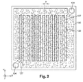
- the figure 2 represents a top view of the resistive element 122.
- the resistive element 122 corresponds to a conductive track extending between the first two conductive vias 124 having a serpentine pattern, which makes it possible to cover the surface lying opposite at least the active part 110 of the electronic circuit. 106.
- the pattern of the resistive element 122 covers almost the entire surface of the rear face of the electronic chip 100.
- the width of the conductive track forming the resistive element 122 and the space between two parallel portions of the conductive track are between about 5 ⁇ m and 50 ⁇ m.
- an FIB attack typically performed on a surface of the electronic chip 100 corresponding to a square of dimensions equal to 50 ⁇ m ⁇ 50 ⁇ m, necessarily gives rise to a significant modification of the electrical resistance of the resistive element 122.
- a space of at least 5 ⁇ m between the different portions of the conductive track makes it possible to allow an etching agent to pass between these portions during a possible etching of the rear face of the electronic chip 100, thereby causing the destruction of the first protective layer 120 and thus also the destruction of the resistive element 122 which is no longer mechanically supported by it.
- the pattern formed by the resistive element 122 at the rear face of the electronic chip 100 is advantageously chosen such that it is sufficiently dense and complex for a "wire detour", that is to say the realization of a metal bridge or a short circuit between two parts of the resistive element 122, or the positioning of equivalent resistance between the first two conductive vias 124, induce a significant variation in the resistance of the resistive element 122 that can be detected.
- the electrical resistance of this resistive element 122 is equal to about 7 ⁇ .
- the value of its electrical resistance becomes infinite. The sensitivity of such a resistive element 122 with respect to a mechanical or chemical attack, or by FIB beam, is therefore much better than for other solutions for protecting the rear face of the chip of the art. prior.
- the pattern formed by the resistive element 122 may be different from a coil, and may correspond to several alternating, intermingled, wound or interlaced patterns in order to make this "wire bend" operation very complicated.
- the dielectric material of the first protective layer 120 is advantageously photosensitive so that it can be insulated and then easily developed to form the locations of the conductive portions 127.
- This dielectric material is for example a vacuum laminated polymer, which makes it possible to fill the space of the first conductive vias 124 not occupied by the dielectric layer 118 and the electrically conductive layer 125.
- the combination of the resistive element 122 and the protective layers 120, 126 makes it possible to optimize the two protection modes conferred by these two elements. Indeed, a chemical or mechanical etching which is the main limit of the protection conferred by a single polymer protective layer, is systematically detected thanks to the damage generated on the resistive element 122. In the case of a mechanical attack of the rear face of the electronic chip 100, it will tear off a portion of the resistive element 122 and create an open circuit between the first conductive vias 124 which will be detected by the electronic chip 100.
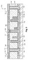
- the figure 3 represents a sectional view of an electronic chip 100 according to a second embodiment.
- the electronic chip 100 in addition to the first conductive vias 124 which electrically connect the resistive element 122 to the electronic circuit 106, the electronic chip 100 also comprises a plurality of second non-emerging vias 128 made from the rear face 117 of the substrate 102 and through a portion of the thickness of the substrate 102, facing the electronic circuit 106 and in particular the active part 110.
- the second vias 128 have depths (dimensions along the Z axis) and dimensions in a plane parallel to the main faces 104 and 117 of the substrate 102 (plane (X, Y)), corresponding to the diameters in the case of second vias 128 substantially circular sections, advantageously different from each other, and for example chosen randomly during their production.
- the depths of the second vias 128 are related to the diameters of the second vias 128, and are chosen in particular as a function of the thickness of the substrate 102.
- the second vias 128 advantageously have diameters of less than about 80 microns and depths of less than about 200 microns. .
- the diameters of the second vias 128 are smaller than those of the first conductive vias 124.
- the sidewalls and the bottom walls of the second vias 128 are covered by the dielectric layer 118.
- the electrically conductive layer 119 here covers continuously the dielectric layer 118 at the side walls and the bottom walls of the vias 128, and at a portion of the rear face 117 of the substrate 102, especially between the second vias 128.
- the presence of the second vias 128 at the rear face of the electronic chip 100 forms a mechanical weakening structure of the substrate 102 to protect the electronic chip 100 against chemical attacks and / or etching attacks FIB.
- the bottom walls of the second or second vias 128 are advantageously close to the electronic circuit 106, for example such that the distance between the electronic circuit 106 of the bottom wall or walls is less than or equal to about 20 microns, or by example between about 10 and 20 microns.
- etching for example with a solution of hydrofluoric acid and nitric acid or potassium hydroxide, in order to etch the substrate 102 from its rear face 117 will result in premature destruction of the electronic circuit 106.
- second vias 128 thus form an additional protection against this type of attack.
- the presence of second vias 128 is penalizing, which also forms additional protection with respect to this type of attack.
- the second or second vias 128 may correspond to one or more trenches formed in a portion of the thickness of the substrate 102.
- the pattern of the resistive element 122 in a plane parallel to the rear face 117 of the substrate 102 may correspond to that of a coil.
- the electronic chip 100 also then comprises an inductive element such as a second coil disposed at the front face of the electronic chip 100, for example integrated in the electronic circuit 106, this second coil being coupled inductively with that formed by the Resistive element 122.
- the resistive element 122 is made such that it is part of an RLC circuit inductively coupled with said inductive element of the front face.
- the resistive element 122 may be in the form of a coil whose ends are electrically connected to each other for example by the electrically conductive layer 119.
- the electronic chip 100 not to comprise the electrically conductive continuous layer 119.
- the protection means of the rear face of the electronic chip 100 are formed by the protective layers 120. , 126, by the resistive element 122, and possibly by the second vias 128.
- the electronic chip 100 it is possible for the electronic chip 100 to have means for protecting its front face, corresponding, for example, to the protection means known from the prior art.
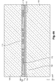
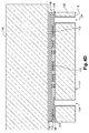
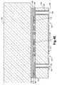
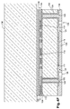
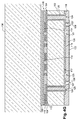
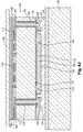
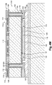
- the Figures 4A to 4N represent steps of a method for producing the electronic chip 100 previously described in connection with the figure 1 .
- the electronic circuit 106 is formed at the front face of the substrate 102 via the implementation of conventional steps of microelectronics.
- the electronic circuit 106 is covered by the passivation layer 114 which forms the front face of the electronic chip 100.
- This front face is secured to a temporary handle 130 formed for example by a silicon substrate, this bonding being for example made between the passivation layer 114 based on oxide and another oxide layer 132 formed beforehand on the temporary handle 130.
- the substrate 102 is then thinned from its rear face until the assembly formed of the substrate 102 and the electronic circuit 106 has a thickness less than or equal to about 200 ⁇ m ( Figure 4B ).
- a hard mask 134 comprising for example an oxide, is then produced on the rear face of the substrate 102.
- the first vias 124 are then formed through the hard mask 134 and the substrate 102 by lithography, etching of the hard mask material 134 and deep etching of the substrate material 102 ( figure 4C ).
- the electronic chip 100 comprises the second vias 128 as in the example of the figure 3
- the second vias 128 and the first vias 124 can be made simultaneously via the implementation of common steps of lithography and etching. Apertures whose dimensions and positioning correspond to those desired for the second vias 128 are thus formed through the hard mask 134.
- the dielectric layer 118 is then deposited, for example by PECVD or SACVD (chemical vapor deposition under sub-atmospheric pressure), as it covers the hard mask 134 disposed on the rear face of the substrate 102, as well as the walls lateral and the bottom walls of the first vias 124 (and possibly second vias 128).
- PECVD chemical vapor deposition under sub-atmospheric pressure
- SACVD chemical vapor deposition under sub-atmospheric pressure
- the first protective layer 120 is then deposited, for example by vacuum rolling, over the entire rear face of the structure previously obtained, that is to say on the electrically conductive layers 119 and 125, as well as at the level of the insulating regions 123 between the layers 119 and 125.
- the material of the first protective layer 120 is deposited such that it fills the first vias 124 (and possibly the second vias 128).
- the first protective layer 120 is etched (or photo-defined if this layer is based on photosensitive material) to form openings 136 opening on the conductive layer 125 at each of the first vias 124, these openings 136 forming the locations of the conductive portions 127 intended to be performed later ( figure 4F ).
- the second protective layer 126 is then deposited, for example via the implementation of a spin coating or by rolling, thus encapsulating the resistive element 122 between the two protective layers 120, 126 ( Figure 4H).
- the second protective layer 126 also covers the conductive portions 127 as well as certain portions of the first protective layer 120.
- the openings 116 are then made through the passivation layer 114, for example by depositing a lithography mask 140 ( figure 4L ) and engraving ( figure 4M ), to form accesses to the contact pads 112.
Landscapes
- Engineering & Computer Science (AREA)
- Computer Security & Cryptography (AREA)
- Computer Networks & Wireless Communication (AREA)
- Signal Processing (AREA)
- Physics & Mathematics (AREA)
- General Physics & Mathematics (AREA)
- Theoretical Computer Science (AREA)
- Semiconductor Integrated Circuits (AREA)
- Parts Printed On Printed Circuit Boards (AREA)
Applications Claiming Priority (1)
| Application Number | Priority Date | Filing Date | Title |
|---|---|---|---|
| FR1553505A FR3035267B1 (fr) | 2015-04-20 | 2015-04-20 | Puce electronique comportant une face arriere protegee |
Publications (3)
| Publication Number | Publication Date |
|---|---|
| EP3086368A2 true EP3086368A2 (de) | 2016-10-26 |
| EP3086368A3 EP3086368A3 (de) | 2017-01-04 |
| EP3086368B1 EP3086368B1 (de) | 2022-12-28 |
Family
ID=53879595
Family Applications (1)
| Application Number | Title | Priority Date | Filing Date |
|---|---|---|---|
| EP16165837.2A Active EP3086368B1 (de) | 2015-04-20 | 2016-04-18 | Elektronischer chip, der eine geschützte rückseite umfasst |
Country Status (4)
| Country | Link |
|---|---|
| US (1) | US9741670B2 (de) |
| EP (1) | EP3086368B1 (de) |
| CN (1) | CN106067460B (de) |
| FR (1) | FR3035267B1 (de) |
Cited By (4)
| Publication number | Priority date | Publication date | Assignee | Title |
|---|---|---|---|---|
| FR3077157A1 (fr) * | 2018-01-25 | 2019-07-26 | Commissariat A L'energie Atomique Et Aux Energies Alternatives | Puce electronique a face arriere protegee |
| WO2019145640A1 (fr) | 2018-01-25 | 2019-08-01 | Commissariat A L'energie Atomique Et Aux Energies Alternatives | Puce electronique a face arriere protegee par une structure de fragilisation amelioree |
| EP3435411B1 (de) * | 2017-07-27 | 2021-03-24 | STMicroelectronics (Crolles 2) SAS | Mikrochip geschützt gegen hackerangriffe von der rückseite |
| US12087708B2 (en) | 2016-08-31 | 2024-09-10 | Stmicroelectronics (Crolles 2) Sas | Chip protected against back-face attacks |
Families Citing this family (16)
| Publication number | Priority date | Publication date | Assignee | Title |
|---|---|---|---|---|
| GB201607589D0 (en) * | 2016-04-29 | 2016-06-15 | Nagravision Sa | Integrated circuit device |
| CN110121858B (zh) * | 2016-12-05 | 2023-03-03 | 密码研究公司 | 背侧安全屏蔽 |
| FR3063385B1 (fr) * | 2017-02-28 | 2019-04-26 | Stmicroelectronics (Rousset) Sas | Circuit integre avec detection d'amincissement par la face arriere et condensateurs de decouplage |
| FR3069954B1 (fr) * | 2017-08-01 | 2020-02-07 | Stmicroelectronics (Rousset) Sas | Procede de detection d'un amincissement du substrat d'un circuit integre par sa face arriere, et circuit integre associe |
| FR3081240B1 (fr) * | 2018-05-15 | 2021-08-06 | St Microelectronics Rousset | Puce electronique |
| WO2020177082A1 (zh) * | 2019-03-05 | 2020-09-10 | 华为技术有限公司 | 一种用于裸片保护的电路、裸片及集成电路 |
| FR3093537B1 (fr) | 2019-03-08 | 2021-06-11 | Safran Aircraft Engines | Sous ensemble de montage d'un palier de guidage d'un arbre de compresseur |
| US11171095B1 (en) | 2020-04-22 | 2021-11-09 | Globalfoundries U.S. Inc. | Active attack prevention for secure integrated circuits using latchup sensitive diode circuit |
| US11121097B1 (en) * | 2020-05-22 | 2021-09-14 | Globalfoundries U.S. Inc. | Active x-ray attack prevention device |
| EP3937055A1 (de) * | 2020-07-10 | 2022-01-12 | Nagravision SA | Integrierte schaltvorrichtung mit schutz gegen bösartige angriffe |
| FR3115125B1 (fr) * | 2020-10-13 | 2023-12-15 | Commissariat Energie Atomique | Boitier-systeme electronique comprenant des faces laterales protegees |
| US11437329B2 (en) * | 2020-10-14 | 2022-09-06 | Globalfoundries U.S. Inc. | Anti-tamper x-ray blocking package |
| US11815717B2 (en) | 2021-11-12 | 2023-11-14 | Globalfoundries U.S. Inc. | Photonic chip security structure |
| US12204144B2 (en) | 2021-11-12 | 2025-01-21 | Globalfoundries U.S. Inc. | Bragg reflector for photonic chip security structure |
| CN116419660B (zh) * | 2021-12-28 | 2026-01-13 | 本源量子计算科技(合肥)股份有限公司 | 量子器件及其制备方法和量子计算机 |
| CN114937650B (zh) * | 2022-07-01 | 2023-10-13 | 今上半导体(信阳)有限公司 | 一种半导体小型化封装结构及其制备方法 |
Citations (2)
| Publication number | Priority date | Publication date | Assignee | Title |
|---|---|---|---|---|
| DE10065339A1 (de) | 2000-12-27 | 2002-07-11 | Infineon Technologies Ag | Kapazitiver Sensor als Schutzvorrichtung gegen Angriffe auf einen Sicherheitschip |
| US8110894B2 (en) | 2003-12-29 | 2012-02-07 | Commissariat A L'energie Atomique | Protection for an integrated circuit chip containing confidential data |
Family Cites Families (8)
| Publication number | Priority date | Publication date | Assignee | Title |
|---|---|---|---|---|
| US5369299A (en) * | 1993-07-22 | 1994-11-29 | National Semiconductor Corporation | Tamper resistant integrated circuit structure |
| EP1400887A1 (de) * | 2002-09-20 | 2004-03-24 | EM Microelectronic-Marin SA | Schutzgerät für einen elektronischen Chip, der vertaulichen Informationen enthält |
| FR2872610B1 (fr) | 2004-07-02 | 2007-06-08 | Commissariat Energie Atomique | Dispositif de securisation de composants |
| US7868441B2 (en) * | 2007-04-13 | 2011-01-11 | Maxim Integrated Products, Inc. | Package on-package secure module having BGA mesh cap |
| CN101772775B (zh) * | 2007-08-02 | 2013-07-10 | Nxp股份有限公司 | 抗篡改半导体器件以及制造该抗篡改半导体器件的方法 |
| US8214657B2 (en) * | 2008-07-29 | 2012-07-03 | International Business Machines Corporation | Resistance sensing for defeating microchip exploitation |
| FR2970116B1 (fr) * | 2011-01-04 | 2013-08-16 | Commissariat Energie Atomique | Procede d'encapsulation d'un microcomposant |
| KR102036919B1 (ko) * | 2013-08-29 | 2019-11-26 | 에스케이하이닉스 주식회사 | 적층 패키지 및 제조 방법 |
-
2015
- 2015-04-20 FR FR1553505A patent/FR3035267B1/fr active Active
-
2016
- 2016-04-18 EP EP16165837.2A patent/EP3086368B1/de active Active
- 2016-04-18 US US15/131,378 patent/US9741670B2/en active Active
- 2016-04-20 CN CN201610249242.3A patent/CN106067460B/zh active Active
Patent Citations (2)
| Publication number | Priority date | Publication date | Assignee | Title |
|---|---|---|---|---|
| DE10065339A1 (de) | 2000-12-27 | 2002-07-11 | Infineon Technologies Ag | Kapazitiver Sensor als Schutzvorrichtung gegen Angriffe auf einen Sicherheitschip |
| US8110894B2 (en) | 2003-12-29 | 2012-02-07 | Commissariat A L'energie Atomique | Protection for an integrated circuit chip containing confidential data |
Cited By (8)
| Publication number | Priority date | Publication date | Assignee | Title |
|---|---|---|---|---|
| US12087708B2 (en) | 2016-08-31 | 2024-09-10 | Stmicroelectronics (Crolles 2) Sas | Chip protected against back-face attacks |
| EP3435411B1 (de) * | 2017-07-27 | 2021-03-24 | STMicroelectronics (Crolles 2) SAS | Mikrochip geschützt gegen hackerangriffe von der rückseite |
| US11387195B2 (en) | 2017-07-27 | 2022-07-12 | Stmicroelectronics (Crolles 2) Sas | Electronic chip |
| FR3077157A1 (fr) * | 2018-01-25 | 2019-07-26 | Commissariat A L'energie Atomique Et Aux Energies Alternatives | Puce electronique a face arriere protegee |
| EP3518282A1 (de) * | 2018-01-25 | 2019-07-31 | Commissariat à l'énergie atomique et aux énergies alternatives | Elektronischer chip, dessen rückseite gegen hacking-angriffe geschütz ist |
| WO2019145640A1 (fr) | 2018-01-25 | 2019-08-01 | Commissariat A L'energie Atomique Et Aux Energies Alternatives | Puce electronique a face arriere protegee par une structure de fragilisation amelioree |
| US11355456B2 (en) | 2018-01-25 | 2022-06-07 | Commissariat A L'energie Atomique Et Aux Energies Alternatives | Electronic chip with protected rear face |
| US11557550B2 (en) | 2018-01-25 | 2023-01-17 | Commissariat A L'energie Atomique Et Aux Energies Alternatives | Electronic chip, the rear face of which is protected by an improved embrittlement structure |
Also Published As
| Publication number | Publication date |
|---|---|
| FR3035267B1 (fr) | 2018-05-25 |
| EP3086368A3 (de) | 2017-01-04 |
| CN106067460B (zh) | 2020-06-30 |
| CN106067460A (zh) | 2016-11-02 |
| US9741670B2 (en) | 2017-08-22 |
| FR3035267A1 (fr) | 2016-10-21 |
| EP3086368B1 (de) | 2022-12-28 |
| US20160307855A1 (en) | 2016-10-20 |
Similar Documents
| Publication | Publication Date | Title |
|---|---|---|
| EP3086368B1 (de) | Elektronischer chip, der eine geschützte rückseite umfasst | |
| EP2866259B1 (de) | Elektronischer Chip mit Mitteln zum Schutz dessen Rückseite | |
| EP3211390B1 (de) | Vorrichtung zur erfassung von elektromagnetischer strahlung mit erhöhter elektrischer lötverbindung | |
| EP2840589B1 (de) | Verbessertes Verfahren zur Trennung zwischen einer aktiven Zone eines Substrats und dessen Rückseite oder eines Teilbereichs seiner Rückseite | |
| EP3944294B1 (de) | Verfahren zur herstellung einer individualisierungszone eines integierten schaltkreises | |
| EP3046147B1 (de) | Elektronischer chip, der mit einer schutzvorrichtung mit phasenwechselmaterial ausgestattet ist, detektionsverfahren eines angriffs auf den chip und herstellungsverfahren dieses chips | |
| FR2971366A1 (fr) | Micro plaquette de semi-conducteur comprenant des moyens de protection contre une attaque physique | |
| EP3637071A1 (de) | Herstellungsverfahren eines detektors von elektromagnetischer strahlung mit verbesserter einkapselungsstruktur | |
| EP3435411B1 (de) | Mikrochip geschützt gegen hackerangriffe von der rückseite | |
| EP1183642B1 (de) | Integrierte schaltkreisanordnung welche gegen angriffe durch kontrollierte zerstörung einer komplementären schicht gesichert ist | |
| EP3864386A1 (de) | Verfahren zur herstellung einer vorrichtung zur detektion elektromagnetischer strahlung mit einem hängenden detektionselement | |
| EP3743942B1 (de) | Elektronischer chip, dessen rückseite durch eine verbesserte versprödungsstruktur geschützt ist | |
| EP3518282B1 (de) | Elektronischer chip, dessen rückseite gegen hacking-angriffe geschütz ist | |
| EP1021833B1 (de) | Gesicherte integrierte halbleiterschaltungsanordnung und herstellungsverfahren | |
| EP0996930A1 (de) | Unterlage für elektrische schaltanordnung mit mitteln die entkoppeln vermeiden | |
| EP3944289A1 (de) | Verfahren zur herstellung einer individualisierungszone eines integierten schaltkreises | |
| EP3739622A1 (de) | Verfahren zur erfassung der möglichen verletzung der integrität eines halbleitersubstrats eines integrierten schaltkreises von seiner rückseite aus, und entsprechender integrierter schaltkreis | |
| EP2960955A1 (de) | Elektrische verbindungsvorrichtung, die verbindungselemente mit einer steuerbaren position umfasst | |
| FR2848025A1 (fr) | Protection d'un composant par nappe conductrice a contact aleatoire | |
| FR3164058A1 (fr) | Dispositif comprenant une piste métallique et procédé de fabrication du dispositif |
Legal Events
| Date | Code | Title | Description |
|---|---|---|---|
| PUAI | Public reference made under article 153(3) epc to a published international application that has entered the european phase |
Free format text: ORIGINAL CODE: 0009012 |
|
| 17P | Request for examination filed |
Effective date: 20160418 |
|
| AK | Designated contracting states |
Kind code of ref document: A2 Designated state(s): AL AT BE BG CH CY CZ DE DK EE ES FI FR GB GR HR HU IE IS IT LI LT LU LV MC MK MT NL NO PL PT RO RS SE SI SK SM TR |
|
| AX | Request for extension of the european patent |
Extension state: BA ME |
|
| RIN1 | Information on inventor provided before grant (corrected) |
Inventor name: BOREL, STEPHAN Inventor name: CHARBONNIER, JEAN |
|
| PUAL | Search report despatched |
Free format text: ORIGINAL CODE: 0009013 |
|
| STAA | Information on the status of an ep patent application or granted ep patent |
Free format text: STATUS: EXAMINATION IS IN PROGRESS |
|
| AK | Designated contracting states |
Kind code of ref document: A3 Designated state(s): AL AT BE BG CH CY CZ DE DK EE ES FI FR GB GR HR HU IE IS IT LI LT LU LV MC MK MT NL NO PL PT RO RS SE SI SK SM TR |
|
| AX | Request for extension of the european patent |
Extension state: BA ME |
|
| RIC1 | Information provided on ipc code assigned before grant |
Ipc: H01L 23/58 20060101AFI20161201BHEP |
|
| 17Q | First examination report despatched |
Effective date: 20161219 |
|
| GRAP | Despatch of communication of intention to grant a patent |
Free format text: ORIGINAL CODE: EPIDOSNIGR1 |
|
| STAA | Information on the status of an ep patent application or granted ep patent |
Free format text: STATUS: GRANT OF PATENT IS INTENDED |
|
| RIC1 | Information provided on ipc code assigned before grant |
Ipc: G09C 1/00 20060101ALI20220706BHEP Ipc: H04L 9/00 20060101ALI20220706BHEP Ipc: H01L 23/58 20060101AFI20220706BHEP |
|
| INTG | Intention to grant announced |
Effective date: 20220722 |
|
| GRAS | Grant fee paid |
Free format text: ORIGINAL CODE: EPIDOSNIGR3 |
|
| GRAA | (expected) grant |
Free format text: ORIGINAL CODE: 0009210 |
|
| STAA | Information on the status of an ep patent application or granted ep patent |
Free format text: STATUS: THE PATENT HAS BEEN GRANTED |
|
| AK | Designated contracting states |
Kind code of ref document: B1 Designated state(s): AL AT BE BG CH CY CZ DE DK EE ES FI FR GB GR HR HU IE IS IT LI LT LU LV MC MK MT NL NO PL PT RO RS SE SI SK SM TR |
|
| REG | Reference to a national code |
Ref country code: GB Ref legal event code: FG4D Free format text: NOT ENGLISH |
|
| REG | Reference to a national code |
Ref country code: CH Ref legal event code: EP |
|
| REG | Reference to a national code |
Ref country code: DE Ref legal event code: R096 Ref document number: 602016077090 Country of ref document: DE |
|
| REG | Reference to a national code |
Ref country code: AT Ref legal event code: REF Ref document number: 1541014 Country of ref document: AT Kind code of ref document: T Effective date: 20230115 |
|
| REG | Reference to a national code |
Ref country code: IE Ref legal event code: FG4D Free format text: LANGUAGE OF EP DOCUMENT: FRENCH |
|
| REG | Reference to a national code |
Ref country code: LT Ref legal event code: MG9D |
|
| PG25 | Lapsed in a contracting state [announced via postgrant information from national office to epo] |
Ref country code: SE Free format text: LAPSE BECAUSE OF FAILURE TO SUBMIT A TRANSLATION OF THE DESCRIPTION OR TO PAY THE FEE WITHIN THE PRESCRIBED TIME-LIMIT Effective date: 20221228 Ref country code: NO Free format text: LAPSE BECAUSE OF FAILURE TO SUBMIT A TRANSLATION OF THE DESCRIPTION OR TO PAY THE FEE WITHIN THE PRESCRIBED TIME-LIMIT Effective date: 20230328 Ref country code: LT Free format text: LAPSE BECAUSE OF FAILURE TO SUBMIT A TRANSLATION OF THE DESCRIPTION OR TO PAY THE FEE WITHIN THE PRESCRIBED TIME-LIMIT Effective date: 20221228 Ref country code: FI Free format text: LAPSE BECAUSE OF FAILURE TO SUBMIT A TRANSLATION OF THE DESCRIPTION OR TO PAY THE FEE WITHIN THE PRESCRIBED TIME-LIMIT Effective date: 20221228 |
|
| REG | Reference to a national code |
Ref country code: NL Ref legal event code: MP Effective date: 20221228 |
|
| REG | Reference to a national code |
Ref country code: AT Ref legal event code: MK05 Ref document number: 1541014 Country of ref document: AT Kind code of ref document: T Effective date: 20221228 |
|
| PG25 | Lapsed in a contracting state [announced via postgrant information from national office to epo] |
Ref country code: RS Free format text: LAPSE BECAUSE OF FAILURE TO SUBMIT A TRANSLATION OF THE DESCRIPTION OR TO PAY THE FEE WITHIN THE PRESCRIBED TIME-LIMIT Effective date: 20221228 Ref country code: LV Free format text: LAPSE BECAUSE OF FAILURE TO SUBMIT A TRANSLATION OF THE DESCRIPTION OR TO PAY THE FEE WITHIN THE PRESCRIBED TIME-LIMIT Effective date: 20221228 Ref country code: HR Free format text: LAPSE BECAUSE OF FAILURE TO SUBMIT A TRANSLATION OF THE DESCRIPTION OR TO PAY THE FEE WITHIN THE PRESCRIBED TIME-LIMIT Effective date: 20221228 Ref country code: GR Free format text: LAPSE BECAUSE OF FAILURE TO SUBMIT A TRANSLATION OF THE DESCRIPTION OR TO PAY THE FEE WITHIN THE PRESCRIBED TIME-LIMIT Effective date: 20230329 |
|
| PG25 | Lapsed in a contracting state [announced via postgrant information from national office to epo] |
Ref country code: NL Free format text: LAPSE BECAUSE OF FAILURE TO SUBMIT A TRANSLATION OF THE DESCRIPTION OR TO PAY THE FEE WITHIN THE PRESCRIBED TIME-LIMIT Effective date: 20221228 |
|
| PG25 | Lapsed in a contracting state [announced via postgrant information from national office to epo] |
Ref country code: SM Free format text: LAPSE BECAUSE OF FAILURE TO SUBMIT A TRANSLATION OF THE DESCRIPTION OR TO PAY THE FEE WITHIN THE PRESCRIBED TIME-LIMIT Effective date: 20221228 Ref country code: RO Free format text: LAPSE BECAUSE OF FAILURE TO SUBMIT A TRANSLATION OF THE DESCRIPTION OR TO PAY THE FEE WITHIN THE PRESCRIBED TIME-LIMIT Effective date: 20221228 Ref country code: PT Free format text: LAPSE BECAUSE OF FAILURE TO SUBMIT A TRANSLATION OF THE DESCRIPTION OR TO PAY THE FEE WITHIN THE PRESCRIBED TIME-LIMIT Effective date: 20230428 Ref country code: ES Free format text: LAPSE BECAUSE OF FAILURE TO SUBMIT A TRANSLATION OF THE DESCRIPTION OR TO PAY THE FEE WITHIN THE PRESCRIBED TIME-LIMIT Effective date: 20221228 Ref country code: EE Free format text: LAPSE BECAUSE OF FAILURE TO SUBMIT A TRANSLATION OF THE DESCRIPTION OR TO PAY THE FEE WITHIN THE PRESCRIBED TIME-LIMIT Effective date: 20221228 Ref country code: CZ Free format text: LAPSE BECAUSE OF FAILURE TO SUBMIT A TRANSLATION OF THE DESCRIPTION OR TO PAY THE FEE WITHIN THE PRESCRIBED TIME-LIMIT Effective date: 20221228 Ref country code: AT Free format text: LAPSE BECAUSE OF FAILURE TO SUBMIT A TRANSLATION OF THE DESCRIPTION OR TO PAY THE FEE WITHIN THE PRESCRIBED TIME-LIMIT Effective date: 20221228 |
|
| PG25 | Lapsed in a contracting state [announced via postgrant information from national office to epo] |
Ref country code: SK Free format text: LAPSE BECAUSE OF FAILURE TO SUBMIT A TRANSLATION OF THE DESCRIPTION OR TO PAY THE FEE WITHIN THE PRESCRIBED TIME-LIMIT Effective date: 20221228 Ref country code: PL Free format text: LAPSE BECAUSE OF FAILURE TO SUBMIT A TRANSLATION OF THE DESCRIPTION OR TO PAY THE FEE WITHIN THE PRESCRIBED TIME-LIMIT Effective date: 20221228 Ref country code: IS Free format text: LAPSE BECAUSE OF FAILURE TO SUBMIT A TRANSLATION OF THE DESCRIPTION OR TO PAY THE FEE WITHIN THE PRESCRIBED TIME-LIMIT Effective date: 20230428 Ref country code: AL Free format text: LAPSE BECAUSE OF FAILURE TO SUBMIT A TRANSLATION OF THE DESCRIPTION OR TO PAY THE FEE WITHIN THE PRESCRIBED TIME-LIMIT Effective date: 20221228 |
|
| REG | Reference to a national code |
Ref country code: DE Ref legal event code: R097 Ref document number: 602016077090 Country of ref document: DE |
|
| PG25 | Lapsed in a contracting state [announced via postgrant information from national office to epo] |
Ref country code: DK Free format text: LAPSE BECAUSE OF FAILURE TO SUBMIT A TRANSLATION OF THE DESCRIPTION OR TO PAY THE FEE WITHIN THE PRESCRIBED TIME-LIMIT Effective date: 20221228 |
|
| PLBE | No opposition filed within time limit |
Free format text: ORIGINAL CODE: 0009261 |
|
| STAA | Information on the status of an ep patent application or granted ep patent |
Free format text: STATUS: NO OPPOSITION FILED WITHIN TIME LIMIT |
|
| REG | Reference to a national code |
Ref country code: CH Ref legal event code: PL |
|
| 26N | No opposition filed |
Effective date: 20230929 |
|
| PG25 | Lapsed in a contracting state [announced via postgrant information from national office to epo] |
Ref country code: LU Free format text: LAPSE BECAUSE OF NON-PAYMENT OF DUE FEES Effective date: 20230418 |
|
| REG | Reference to a national code |
Ref country code: BE Ref legal event code: MM Effective date: 20230430 |
|
| PG25 | Lapsed in a contracting state [announced via postgrant information from national office to epo] |
Ref country code: MC Free format text: LAPSE BECAUSE OF FAILURE TO SUBMIT A TRANSLATION OF THE DESCRIPTION OR TO PAY THE FEE WITHIN THE PRESCRIBED TIME-LIMIT Effective date: 20221228 |
|
| PG25 | Lapsed in a contracting state [announced via postgrant information from national office to epo] |
Ref country code: SI Free format text: LAPSE BECAUSE OF FAILURE TO SUBMIT A TRANSLATION OF THE DESCRIPTION OR TO PAY THE FEE WITHIN THE PRESCRIBED TIME-LIMIT Effective date: 20221228 Ref country code: MC Free format text: LAPSE BECAUSE OF FAILURE TO SUBMIT A TRANSLATION OF THE DESCRIPTION OR TO PAY THE FEE WITHIN THE PRESCRIBED TIME-LIMIT Effective date: 20221228 Ref country code: LI Free format text: LAPSE BECAUSE OF NON-PAYMENT OF DUE FEES Effective date: 20230430 Ref country code: CH Free format text: LAPSE BECAUSE OF NON-PAYMENT OF DUE FEES Effective date: 20230430 |
|
| REG | Reference to a national code |
Ref country code: IE Ref legal event code: MM4A |
|
| PG25 | Lapsed in a contracting state [announced via postgrant information from national office to epo] |
Ref country code: BE Free format text: LAPSE BECAUSE OF NON-PAYMENT OF DUE FEES Effective date: 20230430 |
|
| PG25 | Lapsed in a contracting state [announced via postgrant information from national office to epo] |
Ref country code: IE Free format text: LAPSE BECAUSE OF NON-PAYMENT OF DUE FEES Effective date: 20230418 |
|
| PG25 | Lapsed in a contracting state [announced via postgrant information from national office to epo] |
Ref country code: IE Free format text: LAPSE BECAUSE OF NON-PAYMENT OF DUE FEES Effective date: 20230418 |
|
| PG25 | Lapsed in a contracting state [announced via postgrant information from national office to epo] |
Ref country code: IT Free format text: LAPSE BECAUSE OF FAILURE TO SUBMIT A TRANSLATION OF THE DESCRIPTION OR TO PAY THE FEE WITHIN THE PRESCRIBED TIME-LIMIT Effective date: 20221228 |
|
| PG25 | Lapsed in a contracting state [announced via postgrant information from national office to epo] |
Ref country code: BG Free format text: LAPSE BECAUSE OF FAILURE TO SUBMIT A TRANSLATION OF THE DESCRIPTION OR TO PAY THE FEE WITHIN THE PRESCRIBED TIME-LIMIT Effective date: 20221228 |
|
| PG25 | Lapsed in a contracting state [announced via postgrant information from national office to epo] |
Ref country code: BG Free format text: LAPSE BECAUSE OF FAILURE TO SUBMIT A TRANSLATION OF THE DESCRIPTION OR TO PAY THE FEE WITHIN THE PRESCRIBED TIME-LIMIT Effective date: 20221228 |
|
| PGFP | Annual fee paid to national office [announced via postgrant information from national office to epo] |
Ref country code: DE Payment date: 20250417 Year of fee payment: 10 |
|
| PGFP | Annual fee paid to national office [announced via postgrant information from national office to epo] |
Ref country code: GB Payment date: 20250424 Year of fee payment: 10 |
|
| PGFP | Annual fee paid to national office [announced via postgrant information from national office to epo] |
Ref country code: FR Payment date: 20250422 Year of fee payment: 10 |
|
| PG25 | Lapsed in a contracting state [announced via postgrant information from national office to epo] |
Ref country code: CY Free format text: LAPSE BECAUSE OF FAILURE TO SUBMIT A TRANSLATION OF THE DESCRIPTION OR TO PAY THE FEE WITHIN THE PRESCRIBED TIME-LIMIT; INVALID AB INITIO Effective date: 20160418 |
|
| PG25 | Lapsed in a contracting state [announced via postgrant information from national office to epo] |
Ref country code: HU Free format text: LAPSE BECAUSE OF FAILURE TO SUBMIT A TRANSLATION OF THE DESCRIPTION OR TO PAY THE FEE WITHIN THE PRESCRIBED TIME-LIMIT; INVALID AB INITIO Effective date: 20160418 |
|
| REG | Reference to a national code |
Ref country code: DE Ref legal event code: R079 Ref document number: 602016077090 Country of ref document: DE Free format text: PREVIOUS MAIN CLASS: H01L0023580000 Ipc: H10W0029000000 |
|
| PG25 | Lapsed in a contracting state [announced via postgrant information from national office to epo] |
Ref country code: TR Free format text: LAPSE BECAUSE OF FAILURE TO SUBMIT A TRANSLATION OF THE DESCRIPTION OR TO PAY THE FEE WITHIN THE PRESCRIBED TIME-LIMIT Effective date: 20221228 |