EP3086372A1 - Dispositif d'affichage et son procédé de fabrication - Google Patents
Dispositif d'affichage et son procédé de fabrication Download PDFInfo
- Publication number
- EP3086372A1 EP3086372A1 EP16153285.8A EP16153285A EP3086372A1 EP 3086372 A1 EP3086372 A1 EP 3086372A1 EP 16153285 A EP16153285 A EP 16153285A EP 3086372 A1 EP3086372 A1 EP 3086372A1
- Authority
- EP
- European Patent Office
- Prior art keywords
- substrate
- layer
- emission layer
- display device
- emission
- Prior art date
- Legal status (The legal status is an assumption and is not a legal conclusion. Google has not performed a legal analysis and makes no representation as to the accuracy of the status listed.)
- Withdrawn
Links
- 238000004519 manufacturing process Methods 0.000 title claims description 11
- 239000000758 substrate Substances 0.000 claims abstract description 160
- 239000010410 layer Substances 0.000 claims description 210
- 238000005538 encapsulation Methods 0.000 claims description 47
- 239000011247 coating layer Substances 0.000 claims description 22
- 239000011521 glass Substances 0.000 claims description 20
- 238000000034 method Methods 0.000 claims description 17
- 239000012790 adhesive layer Substances 0.000 claims description 16
- 239000000126 substance Substances 0.000 claims description 7
- 239000005341 toughened glass Substances 0.000 claims description 7
- ZLMJMSJWJFRBEC-UHFFFAOYSA-N Potassium Chemical compound [K] ZLMJMSJWJFRBEC-UHFFFAOYSA-N 0.000 claims description 6
- 229910052700 potassium Inorganic materials 0.000 claims description 6
- 239000011591 potassium Substances 0.000 claims description 6
- 230000003014 reinforcing effect Effects 0.000 claims description 2
- 239000004020 conductor Substances 0.000 description 12
- 239000004065 semiconductor Substances 0.000 description 12
- 238000005192 partition Methods 0.000 description 11
- 230000000903 blocking effect Effects 0.000 description 10
- 238000002161 passivation Methods 0.000 description 9
- VYPSYNLAJGMNEJ-UHFFFAOYSA-N Silicium dioxide Chemical compound O=[Si]=O VYPSYNLAJGMNEJ-UHFFFAOYSA-N 0.000 description 8
- PQXKHYXIUOZZFA-UHFFFAOYSA-M lithium fluoride Chemical compound [Li+].[F-] PQXKHYXIUOZZFA-UHFFFAOYSA-M 0.000 description 8
- 101100027969 Caenorhabditis elegans old-1 gene Proteins 0.000 description 7
- 230000008569 process Effects 0.000 description 7
- 239000003990 capacitor Substances 0.000 description 6
- 150000001875 compounds Chemical class 0.000 description 6
- KPUWHANPEXNPJT-UHFFFAOYSA-N disiloxane Chemical class [SiH3]O[SiH3] KPUWHANPEXNPJT-UHFFFAOYSA-N 0.000 description 6
- 230000010287 polarization Effects 0.000 description 6
- 229910052814 silicon oxide Inorganic materials 0.000 description 6
- 239000012535 impurity Substances 0.000 description 5
- 239000011229 interlayer Substances 0.000 description 5
- 239000004721 Polyphenylene oxide Substances 0.000 description 4
- 239000011575 calcium Substances 0.000 description 4
- 239000004205 dimethyl polysiloxane Substances 0.000 description 4
- 235000013870 dimethyl polysiloxane Nutrition 0.000 description 4
- 230000005611 electricity Effects 0.000 description 4
- 239000000463 material Substances 0.000 description 4
- 229920000435 poly(dimethylsiloxane) Polymers 0.000 description 4
- 229920000570 polyether Polymers 0.000 description 4
- 229920000642 polymer Polymers 0.000 description 4
- 230000003068 static effect Effects 0.000 description 4
- 238000003860 storage Methods 0.000 description 4
- 239000010409 thin film Substances 0.000 description 4
- DGAQECJNVWCQMB-PUAWFVPOSA-M Ilexoside XXIX Chemical compound C[C@@H]1CC[C@@]2(CC[C@@]3(C(=CC[C@H]4[C@]3(CC[C@@H]5[C@@]4(CC[C@@H](C5(C)C)OS(=O)(=O)[O-])C)C)[C@@H]2[C@]1(C)O)C)C(=O)O[C@H]6[C@@H]([C@H]([C@@H]([C@H](O6)CO)O)O)O.[Na+] DGAQECJNVWCQMB-PUAWFVPOSA-M 0.000 description 3
- 239000004642 Polyimide Substances 0.000 description 3
- 229910052581 Si3N4 Inorganic materials 0.000 description 3
- 229910004205 SiNX Inorganic materials 0.000 description 3
- 238000010586 diagram Methods 0.000 description 3
- 238000005259 measurement Methods 0.000 description 3
- 229910021420 polycrystalline silicon Inorganic materials 0.000 description 3
- 229920001721 polyimide Polymers 0.000 description 3
- HQVNEWCFYHHQES-UHFFFAOYSA-N silicon nitride Chemical compound N12[Si]34N5[Si]62N3[Si]51N64 HQVNEWCFYHHQES-UHFFFAOYSA-N 0.000 description 3
- 229910052708 sodium Inorganic materials 0.000 description 3
- 239000011734 sodium Substances 0.000 description 3
- OYPRJOBELJOOCE-UHFFFAOYSA-N Calcium Chemical compound [Ca] OYPRJOBELJOOCE-UHFFFAOYSA-N 0.000 description 2
- 229910052782 aluminium Inorganic materials 0.000 description 2
- XAGFODPZIPBFFR-UHFFFAOYSA-N aluminium Chemical compound [Al] XAGFODPZIPBFFR-UHFFFAOYSA-N 0.000 description 2
- 229910052791 calcium Inorganic materials 0.000 description 2
- 239000003795 chemical substances by application Substances 0.000 description 2
- 239000011651 chromium Substances 0.000 description 2
- 230000007547 defect Effects 0.000 description 2
- 239000010408 film Substances 0.000 description 2
- 239000010931 gold Substances 0.000 description 2
- 125000002887 hydroxy group Chemical group [H]O* 0.000 description 2
- 229910003437 indium oxide Inorganic materials 0.000 description 2
- PJXISJQVUVHSOJ-UHFFFAOYSA-N indium(iii) oxide Chemical compound [O-2].[O-2].[O-2].[In+3].[In+3] PJXISJQVUVHSOJ-UHFFFAOYSA-N 0.000 description 2
- 238000002347 injection Methods 0.000 description 2
- 239000007924 injection Substances 0.000 description 2
- 239000004973 liquid crystal related substance Substances 0.000 description 2
- 239000011777 magnesium Substances 0.000 description 2
- 239000000203 mixture Substances 0.000 description 2
- 239000012044 organic layer Substances 0.000 description 2
- 239000002002 slurry Substances 0.000 description 2
- VYZAMTAEIAYCRO-UHFFFAOYSA-N Chromium Chemical compound [Cr] VYZAMTAEIAYCRO-UHFFFAOYSA-N 0.000 description 1
- WHXSMMKQMYFTQS-UHFFFAOYSA-N Lithium Chemical compound [Li] WHXSMMKQMYFTQS-UHFFFAOYSA-N 0.000 description 1
- FYYHWMGAXLPEAU-UHFFFAOYSA-N Magnesium Chemical compound [Mg] FYYHWMGAXLPEAU-UHFFFAOYSA-N 0.000 description 1
- BQCADISMDOOEFD-UHFFFAOYSA-N Silver Chemical compound [Ag] BQCADISMDOOEFD-UHFFFAOYSA-N 0.000 description 1
- XLOMVQKBTHCTTD-UHFFFAOYSA-N Zinc monoxide Chemical compound [Zn]=O XLOMVQKBTHCTTD-UHFFFAOYSA-N 0.000 description 1
- 239000000654 additive Substances 0.000 description 1
- 230000000996 additive effect Effects 0.000 description 1
- 239000000853 adhesive Substances 0.000 description 1
- 230000001070 adhesive effect Effects 0.000 description 1
- 238000005452 bending Methods 0.000 description 1
- 230000008859 change Effects 0.000 description 1
- 229910052804 chromium Inorganic materials 0.000 description 1
- 239000003086 colorant Substances 0.000 description 1
- 239000000470 constituent Substances 0.000 description 1
- 238000002425 crystallisation Methods 0.000 description 1
- 230000008025 crystallization Effects 0.000 description 1
- 238000005520 cutting process Methods 0.000 description 1
- 238000005137 deposition process Methods 0.000 description 1
- 238000007598 dipping method Methods 0.000 description 1
- 239000012153 distilled water Substances 0.000 description 1
- 230000002708 enhancing effect Effects 0.000 description 1
- 230000007717 exclusion Effects 0.000 description 1
- 230000005669 field effect Effects 0.000 description 1
- PCHJSUWPFVWCPO-UHFFFAOYSA-N gold Chemical compound [Au] PCHJSUWPFVWCPO-UHFFFAOYSA-N 0.000 description 1
- 229910052737 gold Inorganic materials 0.000 description 1
- 230000005484 gravity Effects 0.000 description 1
- AMGQUBHHOARCQH-UHFFFAOYSA-N indium;oxotin Chemical compound [In].[Sn]=O AMGQUBHHOARCQH-UHFFFAOYSA-N 0.000 description 1
- 229910010272 inorganic material Inorganic materials 0.000 description 1
- 239000011147 inorganic material Substances 0.000 description 1
- 238000005342 ion exchange Methods 0.000 description 1
- 229910052744 lithium Inorganic materials 0.000 description 1
- 229910052749 magnesium Inorganic materials 0.000 description 1
- 239000011159 matrix material Substances 0.000 description 1
- 229910052751 metal Inorganic materials 0.000 description 1
- 239000002184 metal Substances 0.000 description 1
- 239000011368 organic material Substances 0.000 description 1
- 229920000058 polyacrylate Polymers 0.000 description 1
- 229920005591 polysilicon Polymers 0.000 description 1
- FGIUAXJPYTZDNR-UHFFFAOYSA-N potassium nitrate Chemical compound [K+].[O-][N+]([O-])=O FGIUAXJPYTZDNR-UHFFFAOYSA-N 0.000 description 1
- -1 region Substances 0.000 description 1
- 239000011347 resin Substances 0.000 description 1
- 229920005989 resin Polymers 0.000 description 1
- 230000004044 response Effects 0.000 description 1
- 239000000377 silicon dioxide Substances 0.000 description 1
- 229910052709 silver Inorganic materials 0.000 description 1
- 239000004332 silver Substances 0.000 description 1
- 238000002834 transmittance Methods 0.000 description 1
- XLYOFNOQVPJJNP-UHFFFAOYSA-N water Chemical compound O XLYOFNOQVPJJNP-UHFFFAOYSA-N 0.000 description 1
- YVTHLONGBIQYBO-UHFFFAOYSA-N zinc indium(3+) oxygen(2-) Chemical compound [O--].[Zn++].[In+3] YVTHLONGBIQYBO-UHFFFAOYSA-N 0.000 description 1
Images





Classifications
-
- H—ELECTRICITY
- H10—SEMICONDUCTOR DEVICES; ELECTRIC SOLID-STATE DEVICES NOT OTHERWISE PROVIDED FOR
- H10K—ORGANIC ELECTRIC SOLID-STATE DEVICES
- H10K59/00—Integrated devices, or assemblies of multiple devices, comprising at least one organic light-emitting element covered by group H10K50/00
- H10K59/10—OLED displays
- H10K59/12—Active-matrix OLED [AMOLED] displays
- H10K59/121—Active-matrix OLED [AMOLED] displays characterised by the geometry or disposition of pixel elements
-
- H—ELECTRICITY
- H10—SEMICONDUCTOR DEVICES; ELECTRIC SOLID-STATE DEVICES NOT OTHERWISE PROVIDED FOR
- H10K—ORGANIC ELECTRIC SOLID-STATE DEVICES
- H10K59/00—Integrated devices, or assemblies of multiple devices, comprising at least one organic light-emitting element covered by group H10K50/00
- H10K59/10—OLED displays
- H10K59/12—Active-matrix OLED [AMOLED] displays
- H10K59/128—Active-matrix OLED [AMOLED] displays comprising two independent displays, e.g. for emitting information from two major sides of the display
-
- H—ELECTRICITY
- H10—SEMICONDUCTOR DEVICES; ELECTRIC SOLID-STATE DEVICES NOT OTHERWISE PROVIDED FOR
- H10K—ORGANIC ELECTRIC SOLID-STATE DEVICES
- H10K50/00—Organic light-emitting devices
- H10K50/80—Constructional details
- H10K50/84—Passivation; Containers; Encapsulations
- H10K50/844—Encapsulations
- H10K50/8445—Encapsulations multilayered coatings having a repetitive structure, e.g. having multiple organic-inorganic bilayers
-
- H—ELECTRICITY
- H10—SEMICONDUCTOR DEVICES; ELECTRIC SOLID-STATE DEVICES NOT OTHERWISE PROVIDED FOR
- H10K—ORGANIC ELECTRIC SOLID-STATE DEVICES
- H10K50/00—Organic light-emitting devices
- H10K50/80—Constructional details
- H10K50/85—Arrangements for extracting light from the devices
-
- H—ELECTRICITY
- H10—SEMICONDUCTOR DEVICES; ELECTRIC SOLID-STATE DEVICES NOT OTHERWISE PROVIDED FOR
- H10K—ORGANIC ELECTRIC SOLID-STATE DEVICES
- H10K59/00—Integrated devices, or assemblies of multiple devices, comprising at least one organic light-emitting element covered by group H10K50/00
- H10K59/10—OLED displays
- H10K59/12—Active-matrix OLED [AMOLED] displays
- H10K59/122—Pixel-defining structures or layers, e.g. banks
-
- H—ELECTRICITY
- H10—SEMICONDUCTOR DEVICES; ELECTRIC SOLID-STATE DEVICES NOT OTHERWISE PROVIDED FOR
- H10K—ORGANIC ELECTRIC SOLID-STATE DEVICES
- H10K59/00—Integrated devices, or assemblies of multiple devices, comprising at least one organic light-emitting element covered by group H10K50/00
- H10K59/10—OLED displays
- H10K59/18—Tiled displays
-
- H—ELECTRICITY
- H10—SEMICONDUCTOR DEVICES; ELECTRIC SOLID-STATE DEVICES NOT OTHERWISE PROVIDED FOR
- H10K—ORGANIC ELECTRIC SOLID-STATE DEVICES
- H10K59/00—Integrated devices, or assemblies of multiple devices, comprising at least one organic light-emitting element covered by group H10K50/00
- H10K59/80—Constructional details
- H10K59/87—Passivation; Containers; Encapsulations
- H10K59/873—Encapsulations
- H10K59/8731—Encapsulations multilayered coatings having a repetitive structure, e.g. having multiple organic-inorganic bilayers
-
- H—ELECTRICITY
- H10—SEMICONDUCTOR DEVICES; ELECTRIC SOLID-STATE DEVICES NOT OTHERWISE PROVIDED FOR
- H10K—ORGANIC ELECTRIC SOLID-STATE DEVICES
- H10K71/00—Manufacture or treatment specially adapted for the organic devices covered by this subclass
-
- H—ELECTRICITY
- H10—SEMICONDUCTOR DEVICES; ELECTRIC SOLID-STATE DEVICES NOT OTHERWISE PROVIDED FOR
- H10K—ORGANIC ELECTRIC SOLID-STATE DEVICES
- H10K59/00—Integrated devices, or assemblies of multiple devices, comprising at least one organic light-emitting element covered by group H10K50/00
- H10K59/10—OLED displays
- H10K59/12—Active-matrix OLED [AMOLED] displays
Definitions
- the invention relates to a display device and a manufacturing method thereof.
- a display device mainly uses a flat panel display, such as a liquid crystal display, an organic light emitting device, or a plasma display, for example.
- an organic light emitting device includes two electrodes and an organic emission layer interposed therebetween, electrons injected from one electrode and holes injected from the other electrode are combined in the organic emission layer to form excitons, and the excitons release energy to emit light.
- the display device includes a light emission region and a bezel region as a non-light emission region surrounding the light emission region.
- a signal processing circuit to drive the plurality of pixels is positioned in the display area and an edge of an encapsulation layer to protect the plurality of pixels is positioned in the bezel region. Efforts to minimize the bezel region in order to maximize the light emission region are being further researched.
- the invention provides a display device for the removal of a non-light emitting region, along with a manufacturing method thereof.
- a display device includes a first substrate, a first emission layer disposed on the first substrate and emitted by a top emission type, a second substrate facing the first substrate and covering the first substrate, and a second emission layer disposed under the second substrate and emitted by a bottom emission type, wherein the portion of the first emission layer and the portion of the second emission layer overlap each other.
- the first substrate may include a first center portion and a first outer portion enclosing the first center portion
- the second substrate may include a second center portion, a second outer portion enclosing the second center portion, and an overlapping portion between the second center portion and the second outer portion
- the second emission layer may be disposed under the second outer portion and the overlapping portion
- the first substrate and second substrate may respectively include thin glasses having a thickness of about 50 micrometers ( ⁇ m) to about 100 ⁇ m.
- the first substrate and the second substrate may be respectively chemical tempered glasses including a potassium factor.
- the overlapping portion and the first outer portion may overlap each other.
- the portion of the first emission layer positioned at the first outer portion and the portion of the second emission layer positioned at the overlapping portion may overlap each other.
- a first encapsulation layer covering the first emission layer, a second encapsulation layer covering the second emission layer and the second substrate, and an adhesive layer adhering the first encapsulation layer and the second encapsulation layer to each other may be further included.
- the second center portion of the second substrate may contact the second encapsulation layer.
- the thickness of the adhesive layer positioned in the second center portion of the second substrate may be larger than the thickness of the adhesive layer positioned in the second outer portion and the overlapping portion of the second substrate.
- the first emission layer may include a plurality of first pixels
- the second emission layer may include a plurality of second pixels
- a boundary portion interval serving as an interval between a second outermost pixel, which is the outermost pixel among the plurality of second pixels, and the first pixel closest to the second outermost pixel among the plurality of first pixels on a plane surface may be substantially the same as the center portion interval serving as the interval between the adjacent first pixels among the plurality of first pixels.
- the first pixel may only be positioned in the first center portion.
- the first pixel may be positioned at the first center portion and the first outer portion.
- the first pixel may include a first driving transistor disposed on the first substrate and a first organic light emitting diode connected to the first driving transistor
- the second pixel may include a second driving transistor disposed on the second substrate and a second organic light emitting diode connected to the second driving transistor, and the light emitted from the first organic light emitting diode and the second organic light emitting diode may pass through the second substrate to be irradiated.
- a polarizer disposed on the second substrate may be further included.
- the polarizer may include a light blocking member that is disposed on the second substrate and has a plurality of light blocking openings, and a color filter disposed in the plurality of light blocking openings.
- a first hard coating layer disposed on the polarizer may be further included.
- a touch sensor disposed on the first hard coating layer may be further included.
- a second hard coating layer disposed on the touch sensor may be further included.
- a manufacturing method of a display device includes forming a first emission layer emitting light by a top emission type on a first substrate, forming a first encapsulation layer covering the first emission layer, forming a second emission layer emitting the light by a bottom emission type on the second outer portion and the overlapping portion of the second substrate, covering a second encapsulation layer covering the second emission layer, and turning the second substrate and interposing an adhesive layer between the first encapsulation layer and the second encapsulation layer to adhere the first encapsulation layer and the second encapsulation layer, wherein the portion of the first emission layer and the portion of the second emission layer overlap each other.
- the method may further include chemically reinforcing the first substrate and the second substrate
- the first substrate and second substrate may include a thin glass having a thickness of about 50 micrometers ( ⁇ m) to about 100 ⁇ m, respectively.
- the first substrate may include a first center portion and a first outer portion enclosing the first center portion
- the second substrate may include a second center portion, a second outer portion enclosing the second center portion, and an overlapping portion between the second center portion and the second outer portion
- the second emission layer may be disposed under the second outer portion and the overlapping portion
- the overlapping portion and the first outer portion may overlap each other.
- the portion of the first emission layer positioned at the first outer portion and the portion of the second emission layer positioned at the overlapping portion may overlap each other.
- the method may further include forming a polarization layer on the second substrate and forming a first hard coating layer on the polarization layer.
- the method may further include forming a touch sensor on the first hard coating layer and forming a second hard coating layer on the touch sensor.
- the second center portion of the second substrate is used as a window for the top emission and the second outer portion, and the overlapping portion of the second substrate is simultaneously used as the substrate for the bottom emission, thereby maximizing the emission region.
- the portion of the first emission layer of the first substrate and the portion of the second emission layer of the second substrate overlap each other, and the center portion interval between the first pixels or the second pixels and the boundary portion interval between the first pixel and the second pixel are provided to be substantially the same in order to not recognize the boundary portion between the first pixel and the second pixel, such that the first emission layer of the top emission and the second emission layer of the bottom emission may be not distinguished. Accordingly, the display quality may be improved.
- first substrate and the second substrate including thin glass are chemically reinforced, or the first hard coating layer and the second hard coating layer are disposed on the second substrate, thereby simultaneously satisfying the flexibility and the hardness of the display device.
- the word “comprise” and variations such as “comprises” or “comprising” will be understood to imply the inclusion of stated elements but not the exclusion of any other elements.
- the word “on” means positioning on or below the object portion, and does not necessarily mean positioning on the upper side of the object portion based on a direction of gravity.
- the word “on a flat surface” means when an object portion is viewed from above, and the word “on a cross section” means when a cross section taken by vertically cutting an object portion is viewed from the side.
- the invention is not limited to the number of thin film transistors TFT and capacitors illustrated in the accompanying drawings, and the organic light emitting diode display may include a plurality of thin film transistors and one or more capacitors in one pixel, and a separate wire may be further provided or a known wire may be omitted to provide various structures.
- the pixel means a minimum unit displaying an image
- the display device displays an image through a plurality of pixels.
- relative terms such as “lower” or “bottom” and “upper” or “top,” may be used herein to describe one element's relationship to another element as illustrated in the Figures. It will be understood that relative terms are intended to encompass different orientations of the device in addition to the orientation depicted in the Figures. For example, if the device in one of the figures is turned over, elements described as being on the “lower” side of other elements would then be oriented on “upper” sides of the other elements. The exemplary term “lower,” can therefore, encompasses both an orientation of “lower” and “upper,” depending on the particular orientation of the figure.
- Exemplary embodiments are described herein with reference to cross section illustrations that are schematic illustrations of idealized embodiments. As such, variations from the shapes of the illustrations as a result, for example, of manufacturing techniques and/or tolerances, are to be expected. Thus, embodiments described herein should not be construed as limited to the particular shapes of regions as illustrated herein but are to include deviations in shapes that result, for example, from manufacturing. For example, a region illustrated or described as flat may, typically, have rough and/or nonlinear features. Moreover, sharp angles that are illustrated may be rounded. Thus, the regions illustrated in the figures are schematic in nature and their shapes are not intended to illustrate the precise shape of a region and are not intended to limit the scope of the present claims.
- FIG. 1 is a schematic top plan view of a display device according to an exemplary embodiment of the invention
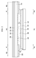
- FIG. 2 is a schematic cross-sectional view of a display device according to an exemplary embodiment of the invention
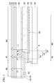
- FIG. 3 is an enlarged cross-sectional view of one end portion of FIG. 2
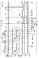
- FIG. 4 is an enlarged top plan view of a portion A of FIG. 1
- FIG. 5 is an equivalent circuit diagram of one pixel of a display device according to an exemplary embodiment of the invention
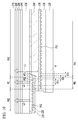
- FIG. 6 is an enlarged top plan view of a portion B of FIG. 3 .
- a display device includes a first substrate 110, a first emission layer 120 disposed on the first substrate 110, a first encapsulation layer 130 covering the first emission layer 120, a second substrate 210 facing the first substrate 110 and covering the first substrate 110, a second emission layer 220 disposed under the second substrate 210, a second encapsulation layer 230 covering the second emission layer 220 and the second substrate 210, an adhesive layer 300 interposed between the first encapsulation layer 130 and the second encapsulation layer 230 and adhering the first encapsulation layer 130 and the second encapsulation layer 230.
- the first substrate 110 may include a thin glass having a thickness of about 50 micrometers ( ⁇ m) to about 100 ⁇ m, for example.
- the first substrate 110 includes a polymer such as PI to improve flexibility, when hardening the polymer, many impurities are generated such that there are a large number of process defects, and the surface charges are increased such that static electricity is generated, thereby requiring the management of foreign matter.
- the impurities and static electricity are not generated such that the additional management of foreign matter is not required.
- the first substrate 110 is stronger than when including a polyimide such that the impact reliability is also high.
- the first substrate 110 includes a first center portion PA1 and a first outer portion PB1 enclosing the first center portion PA1.
- This first substrate 110 may be a chemical tempered glass.
- Chemical tempered glass is a glass with a surface hardness that is enhanced by replacing a sodium factor as one basic component of the glass composition with a potassium factor to generate a compress stress in the surface of the glass.
- first emission layer 120 of the first substrate 110 is disposed in a position corresponding to the first center portion PA1 and first outer portion PB1.
- the first emission layer 120 includes a plurality of first pixels PX1 emitting light through a top surface.
- the plurality of first pixels PX1 is disposed at one position corresponding to the first center portion PA1.
- the first encapsulation layer 130 is a thin film encapsulation layer in which an organic layer and an inorganic layer are alternately deposited and may be transparent.
- the second substrate 210 has a larger area than the first substrate 110 and covers the entire first substrate 110.
- the second substrate 210 includes a second center portion PA2 overlapping the first center portion PA1 of the first substrate 110, a second outer portion PB2 that does not overlap the first substrate 110, and an overlapping portion PC overlapping the first outer portion PB1 of the first substrate 110.
- the second substrate 210 may include thin glass having a thickness of about 50 ⁇ m to about 100 ⁇ m, for example.
- the second substrate 210 includes a polymer such as PI to improve flexibility, when hardening the polymer, many impurities are generated such that there is a large number of process defects, and the surface charges are increased such that static electricity is generated, thereby requiring the management of foreign matter.
- the impurities and static electricity are not generated such that the additional management of foreign matter is not required.
- the second substrate 210 includes thin glass, the first substrate 110 is stronger than when including a polyimide, such that the impact reliability is also high.
- the second substrate 210 may be chemical tempered glass including the potassium factor. Chemical tempered glass is thinner than general tempered glass and is equal to or greater than 1.7 times stronger, and there is no shrinkage or warping phenomena caused by the process.
- the second emission layer 220 is disposed at a position corresponding to the second outer portion PB2 and the overlapping portion PC of the second substrate 210.
- the second emission layer 220 includes a plurality of second pixels PX2 emitting light to a rear surface through the second substrate 210.
- the plurality of second pixels PX2 is disposed at a position corresponding to the second outer portion PB2 and the overlapping portion PC.
- the second encapsulation layer 230 covers the second emission layer 220 at the position corresponding to the second outer portion PB2 and the overlapping portion PC of the second substrate 210, but directly contacts the surface of the second center portion PA2 at the position corresponding to the second center portion PA2 of the second substrate 210.
- the second encapsulation layer 230 is a thin film encapsulation layer in which an organic layer and an inorganic layer are alternately deposited and may be transparent.
- the adhesive layer 300 as an optically clear adhesive (“OCA”) functions like glass with equal to or greater than about 97 percent (%) light transmittance and simultaneously has adhesiveness, for example.
- OCA optically clear adhesive
- a light L1 generated from the first emission layer 120 is irradiated to the top surface and passes the second center portion PA2 of the second substrate 210
- a light L2 generated from the second emission layer 220 is irradiated to the rear surface and passes the second outer portion PB2 and the overlapping portion PC of the second substrate 210. Accordingly, the light passes through all of the second center portion PA2, the second outer portion PB2, and the overlapping portion PC of the second substrate 210 such that the non-light emitting region does not exist in the second substrate 210.
- the second center portion PA2 of the second substrate 210 is used as a window of the top emission, and the second outer portion PB2 and the overlapping portion PC of the second substrate 210 are simultaneously used as the substrate of the bottom emission, thereby maximizing the emission region.
- the overlapping portion PC of the second substrate 210 and the first outer portion PB1 of the first substrate 110 overlap each other. Accordingly, a portion of the first emission layer 120 and a portion of the second emission layer 220 overlap each other. In this case, the first pixel PX1 is not disposed in the first emission layer 120 of the position corresponding to the first outer portion PB1.
- a center portion interval d1x and d1y when an interval between the adjacent first pixels PX1 among the plurality of first pixels PX1 and the interval between the adjacent second pixel PX2 among the plurality of second pixels PX2 are referred to as a center portion interval d1x and d1y, and the interval between the second outermost pixel PT2, which is the outermost positioned pixel among the plurality of second pixels PX2, and the first adjacent pixel PT1, which is closest to the second outermost pixel PT2 among the plurality of first pixels PX1 on the plane surface, is referred to as a boundary portion interval d2x and d2y, the center portion interval d1x and d1y and the boundary portion interval d2x and d2y may be substantially the same.
- a transverse boundary portion interval d2x between the first adjacent pixel PT1 and the second outermost pixel PT2 closest thereto in the horizontal direction on the plane surface is substantially the same as a transverse center portion interval d1x of a horizontal direction interval between the first pixels PX1 or the second pixels PX2.
- a longitudinal boundary portion interval d2y between the first adjacent pixel PT1 and the second outermost pixel PT2 closest thereto in the vertical direction on the plane surface is substantially the same as the center portion interval d1y of the vertical direction interval between the first pixels PX1 or the second pixels PX2.
- the center portion intervals d1x and d1y between the first pixels PX1 or the second pixels PX2 and the boundary portion intervals d2x and d2y between the first pixel PX1 and the second pixel PX2 are substantially the same as each other, the boundary portion between the first pixel PX1 and the second pixel PX2 positioned at different substrates is not recognized, and thereby the first emission layer 120 of the top emission and the second emission layer 220 of the bottom emission cannot be distinguished from each other. Accordingly, the display quality may be improved.
- the boundary portion between the first pixel PX1 and the second pixel PX2 is not recognized such that the display quality may be improved.
- first encapsulation layer 130 and the second encapsulation layer 230 are transparent such that the overlapping portion PC is not recognized even though the first substrate 110 and the second substrate 210 partially overlap, thereby improving the display quality.
- the detailed structure of the first emission layer 120 and the second emission layer 220 will be described with reference to FIGS. 5 and 6 .
- the structure will be described regarding the driving transistor, since the switching transistor has substantially the same stack structure as that of the driving transistors, and thus a duplicate description thereof will be omitted.
- FIG. 5 is an equivalent circuit diagram of one pixel of a display device according to an exemplary embodiment of the invention.
- a display device includes a plurality of signal lines 21, 71, and 72, and a plurality of pixels PX connected to the plurality of signal lines and arranged in an approximate matrix type.
- the plurality of pixels PX includes a first pixel PX1 (refer to FIG. 6 ) in which the first emission layer 120 (refer to FIG. 6 ) is disposed and a second pixel PX2 in which the second emission layer 220 (refer to FIG. 6 ) is disposed.
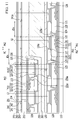
- the signal lines 21, 71, and 72 include a plurality of scan lines 21 transmitting a scan signal Sn, a plurality of data lines 71 crossing the scan lines 21 and transmitting a data signal Dm, and a plurality of driving voltage lines 72 transmitting a driving voltage ELVDD and which are substantially parallel to the data lines 71.
- the gate lines 21 extend substantially parallel to one another in a row direction
- the data lines 71 and the driving voltage lines 72 extend substantially parallel to one another in a column direction.
- Each pixel PX includes a plurality of transistors T1 and T2 respectively connected to the plurality of signal lines 21, 71, and 72, a storage capacitor Cst, and an organic light emitting diode OLD.
- the transistors T1 and T2 include a switching transistor T1 connected to the data line 71, and a driving transistor T2 connected to the organic light emitting diode OLD.
- the driving transistor T2 includes a first driving transistor T21 (refer to FIG. 6 ) in which the first emission layer 120 is disposed and a second driving transistor T22 (refer to FIG. 6 ) in which the second emission layer 220 is disposed.
- the switching transistor T1 includes a control terminal, an input terminal, and an output terminal, and the control terminal thereof is connected to the scan line 21, the input terminal thereof is connected to the data line 71, and the output terminal thereof is connected to the driving transistor T2.
- the switching transistor T1 transmits the data signal Dm applied to the data line 71 to the driving transistor T2 in response to the scan signal Sn applied to the scan line 21.
- the driving transistor T2 also includes a control terminal, an input terminal, and an output terminal, and the control terminal thereof is connected to the switching transistor T1, the input terminal thereof is connected to the driving voltage line 72, and the output terminal thereof is connected to the organic light emitting diode OLD.
- the driving transistor T2 allows a driving current Id, which has a level varying according to a voltage applied between the control terminal and the output terminal, to flow.
- the storage capacitor Cst is connected between the control terminal and the input terminal of the driving transistor T2.
- the storage capacitor Cst charges the data signal applied to the control terminal of the driving transistor T2 and maintains the data signal even after the switching transistor T1 is turned off.
- the organic light emitting diode OLD includes an anode that is connected to the output terminal of the driving transistor T2, and a cathode that is connected to the common voltage ELVSS.
- the organic light emitting diode OLD emits light with an intensity varying according to the driving current Id of the driving transistor T2, thereby displaying an image.
- the organic light emitting diode OLD includes a first organic light emitting diode OLD1 (refer to FIG.6 ) in which the first emission layer 120 is disposed and a second organic light emitting diode OLD2 (refer to FIG.6 ) in which the second emission layer 220 is disposed.
- the switching transistor T1 and the driving transistor T2 may be an n-channel field effect transistor ("FET") or a p-channel FET.
- FET field effect transistor
- a connection relationship among the transistors T1 and T2, the storage capacitor Cst, and the organic light emitting diode OLD may be changed.
- FIG. 6 is an enlarged cross-sectional view of a portion of FIG. 3 .
- a first buffer layer 121 is disposed on the first substrate 110.
- the first buffer layer 120 may serve to improve a characteristic of the polycrystalline silicon and reduce stress applied to the semiconductor 122 disposed on the buffer 121 by blocking impurities from the first substrate 110 and flattening the first substrate 110 during a crystallization process for forming polycrystalline silicon.
- the first buffer layer 121 may include silicon nitride (SiNx) or silicon oxide (SiO2), for example.
- a first semiconductor 122 is disposed on the first buffer layer 121.
- the first semiconductor 122 may include polysilicon or an oxide semiconductor, for example.
- a first gate insulating layer 123 covering the first semiconductor 122 is disposed thereon.
- the first gate insulating layer 123 may include silicon nitride (SiNx) or silicon oxide (SiO2), or the like, for example.
- a first gate electrode G1 is disposed on the first gate insulating layer 123.
- the first gate electrode G1 is a part of the scan line 21 and overlaps the first semiconductor 122.
- a first interlayer insulating layer 124 covering the first gate electrode G1 is disposed thereon.
- the first interlayer insulating layer 124 may include silicon nitride (SiNx) or silicon oxide (SiO2) like the first gate insulating layer 123, for example.
- a first source electrode S1 and a first drain electrode D1 are disposed on the first interlayer insulating layer 124.
- the first source electrode S1 and the first drain electrode D1 are respectively connected to the source region and the drain region of the first semiconductor 122.
- the first gate electrode G1, the first source electrode S1, and the first drain electrode D1 provide a first driving transistor T21.
- a first passivation layer 125 covering the first source electrode S1 and the first drain electrode D1 is disposed thereon.
- a first pixel electrode 127 including a reflective conductive material such as lithium (Li), calcium (Ca), lithium fluoride/calcium (LiF/Ca), lithium fluoride /aluminum (LiF/Al), aluminum (Al), silver (Ag), magnesium (Mg), or gold (Au) is disposed on the first passivation layer 125.
- the first pixel electrode 127 is electrically connected to the first drain electrode D1 of the first driving transistor T21 through the contact hole 125a defined in the passivation layer 125, thereby being an anode of the first organic light emitting diode OLD 1.
- a first partition 126 is disposed on the first passivation layer 125 and the edge of the first pixel electrode 127.
- the first partition 126 has a first pixel opening 126a exposing the first pixel electrode 127.
- the first partition 126 may be provided to include a resin, such as polyacrylates or polyimides, and a silica-based inorganic material, or the like.
- the first organic emission layer 128 is disposed in the first pixel opening 126a of the first partition 126.
- the first organic emission layer 128 is disposed in multiple layers including one or more of a light emission layer, a hole injection layer (“HIL”), a hole transporting layer (“HTL”), an electron transporting layer (“ETL”), and an electron injection layer (“EIL”).
- HIL hole injection layer
- HTL hole transporting layer
- ETL electron transporting layer
- EIL electron injection layer
- a first common electrode 129 including a transparent conductive material such as indium tin oxide (“ITO"), indium zinc oxide (“IZO”), zinc oxide (ZnO), or indium oxide (In2O3) is disposed on the first partition 126 and the first organic emission layer 128.
- the first common electrode 129 becomes a cathode of the first organic light emitting diode OLD.
- the first pixel electrode 127, the first organic emission layer 128, and the first common electrode 129 together provide a first organic light emitting diode OLD1.
- the first organic light emitting diode OLD1 includes the first pixel electrode 127 including a reflection conductive material and the first common electrode 129 including the transparent conductive material such that the light L1 emitted from the first organic emission layer 128 is reflected on the first pixel electrode 127 and passes through the first common electrode 129. Accordingly, the light L1 emitted from the first organic emission layer 128 passes through the second center portion PA2 of the second substrate 210.
- a second buffer layer 221 is disposed under the second substrate 210.
- a second semiconductor 222 is disposed on the second buffer layer 221.
- a second gate insulating layer 223 covering the second semiconductor 222 is disposed on the second semiconductor 222.
- a second gate electrode G2 is disposed on the second gate insulating layer 223. The first gate electrode G1 is part of the scan line 21 and partially overlaps the second semiconductor 222.
- a second interlayer insulating layer 224 covering the second gate electrode G2 is disposed thereunder.
- a second source electrode S2 and a second drain electrode D2 are disposed under the second interlayer insulating layer 224.
- the second source electrode S2 and the second drain electrode D2 are respectively connected to the source region and the drain region of the second semiconductor 222.
- the second gate electrode G2, the second source electrode S2, and the second drain electrode D2 provide a second driving transistor T22.
- a second passivation layer 225 covering the second source electrode S2 and the second drain electrode D2 is disposed thereunder.
- a second pixel electrode 227 including the transparent conductive material is disposed under the second passivation layer 225.
- the second pixel electrode 227 is electrically connected to the second drain electrode D2 of the second driving transistor T22 through the contact hole 225a defined in the second passivation layer 225, thereby being the anode of the second organic light emitting diode OLD2.
- a second partition 226 is disposed on the second passivation layer 225 and the edge of the second pixel electrode 227.
- the second partition 226 has a second pixel opening 226a exposing the first pixel electrode 127.
- a second organic emission layer 228 is disposed in the second pixel opening 226a of the second partition 226.
- the second organic emission layer 228 is disposed in multiple layers including one or more of a light emission layer, an HIL, an HTL, an ETL, and an EIL.
- second organic emission layer 228 includes all of the light emission layer, the HIL, the HTL, the ETL, and the EIL, the HIL is positioned on the second pixel electrode 227, which is the anode, and the HTL, the light emission layer, the ETL, and the EIL are sequentially stacked on the HIL.
- a second common electrode 229 including the reflective conductive material is disposed under the second partition 226 and the second organic emission layer 228.
- the second common electrode 229 becomes the cathode of the second organic light emitting diode OLD2.
- the second pixel electrode 227, the second organic emission layer 228, and the second common electrode 229 together provide the second organic light emitting diode OLD2. Since the second organic light emitting diode OLD2 includes a second pixel electrode 227 including the transparent conductive material and a second common electrode 229 including the reflective conductive material, the light L2 emitted from the second organic emission layer 228 passes through the second pixel electrode 227 and is reflected by the second common electrode 229. Accordingly, the light L2 emitted from the second organic emission layer 228 passes through the second outer portion PB2 and the overlapping portion PC of the second substrate 210.
- the first pixel PX1 including the first driving transistor T21 and the first organic light emitting diode OLD1 is only provided at the position corresponding to the first center portion PA1 of the first substrate 110, but is not provided at the position corresponding to the first outer portion PB1 of the first substrate 110.
- the second pixel PX2 including the second driving transistor T22 and the second organic light emitting diode OLD2 is provided at the position corresponding to the overlapping portion PC and the second outer portion PB2 (refer to FIGS. 1 to 3 ) of the second substrate 210.
- the transverse boundary portion interval d2x between the first adjacent pixel PT1 (refer to FIG. 4 ) and the second outermost pixel PT2 (refer to FIG. 4 ) closest thereto in the horizontal direction on the plane surface is substantially the same as the transverse center portion interval d1x of the horizontal direction interval between the first pixels PX1.
- the boundary portion between the first pixel PX1 and the second pixel PX2 is not recognized such that the first emission layer 120 of the top emission and the second emission layer 220 of the bottom emission may not be distinguished from each other. Accordingly, the display quality may be improved.
- An adhesive layer 300 is disposed between the first encapsulation layer 130 and the second encapsulation layer 230.
- the second encapsulation layer 230 covering the end of the second emission layer 220 covers the inclined side wall of the second emission layer 220, and the second encapsulation layer 230 contacts the surface of the second substrate 210.
- a polarization layer 240 to remove the reflection of the external light is disposed on the second substrate 210.
- the polarization layer 240 is disposed on the second substrate 210 and includes a light blocking member 241 blocking the light and a color filter 242 is disposed in a plurality of light blocking openings 241a of the light blocking member 241.
- the light blocking member 241 may include a metal such as chromium (Cr) or an organic material, and the color filter 242 may overlap a portion of the light blocking member 241.
- a first hard coating layer 250 is disposed on the polarization layer 240.
- the first hard coating layer 250 includes a siloxane-based compound
- the siloxane-based compound includes any one of poly ether modified poly dimethyl siloxane or poly dimethyl siloxane of a poly ether modified hydroxyl functional group, or a combination of two or more thereof, that is, examples of the siloxane-based compound include BYK-306 (BYK chemi agent), BYK-307, BYK-308, BYK-310, BYK-330, BYK-333, BYK-341, and BYK-344.
- a touch sensor 260 is disposed on the first hard coating layer 250.
- the touch sensor 260 adhered under the second substrate 210 as an input device of the display device inputs the information through a screen being directly contacted by a finger or a pen.
- the touch sensor 260 may be a capacitive type sensing a position where a capacitance change is generated according to the contact on two electrodes separated from each other.
- a second hard coating layer 270 is disposed on the touch sensor 260.
- the second hard coating layer 270 includes a siloxane-based compound
- the siloxane-based compound may include any one among poly ether modified poly dimethyl siloxane or a poly dimethyl siloxane of poly ether modified hydroxyl functional group, or a combination of two or more thereof, that is, examples of the siloxane-based compound include BYK-306 (BYK chemi agent), BYK-307, BYK-308, BYK-310, BYK-330, BYK-333, BYK-341, and BYK-344.
- the hardness of the second substrate 210 as the glass substrate having a thin thickness of about 50 ⁇ m to about 100 ⁇ m, for example, may be improved.
- the second hard coating layer 270 may be omitted.
- FIGS. 7 , 8 , and 9 are cross-sectional views sequentially showing a manufacturing method of a display device according to an exemplary embodiment of the invention.
- the first substrate 110 and the second substrate 210 are chemically enhanced by replacing a sodium factor with a potassium factor in the first substrate 110 and second substrate 210.
- a chemical enhancing method a slurry process using an ion exchange slurry, a dipping process enabling the reuse of a potassium nitrate salt, or a deposition process reducing a material and simplifying the process without a oxide-based additive or a distilled water is used, for example.
- the first substrate 110 and the second substrate 210 include a glass, and the surface hardness thereof is enhanced by replacing a sodium factor as one of basic components of a glass composition with a potassium factor to generate a compress stress in the surface of the glass. Accordingly, by manufacturing the first substrate 110 and the second substrate 220 including thin glass having a thickness of about 50 ⁇ m to about 100 ⁇ m, for example, the flexibility may be improved and the hardness may be improved.
- the first emission layer 120 of the top emission type is disposed on the first substrate 110. Also, the first encapsulation layer 130 covering the first emission layer 120 is provided.
- the second emission layer 220 of the bottom emission type through the second substrate 210 is disposed on the second outer portion PB2 and the overlapping portion PC of the second substrate 210. Also, the second encapsulation layer 230 covering the second emission layer 220 is provided.
- the second substrate 210 is turned and the adhesive layer 300 is interposed between the first encapsulation layer 130 and the second encapsulation layer 230 to adhere the first encapsulation layer 130 and the second encapsulation layer 230.
- the portion of the first emission layer 120 and the portion of the second emission layer 220 overlap each other.
- the thickness t1 of the adhesive layer 300 positioned in the second center portion PA2 of the second substrate 210 may be larger than the thickness t2 of the adhesive layer positioned in the second outer portion PB2 and the overlapping portion PC of the second substrate 210.
- the boundary portion between the first pixel PX1 and the second pixel PX2 positioned in the different substrates is not recognized such that the first emission layer 120 of the top emission and the second emission layer 220 of the bottom emission may not be distinguished from each other.
- the polarization layer 240, the first hard coating layer 250, the touch sensor 260, and the second hard coating layer 270 are sequentially provided.
- the hardness of the second substrate 210 as a thin glass substrate having a thickness of about 50 ⁇ m to about 100 ⁇ m may be improved, for example.
- the first pixel may not be disposed in the first emission layer of the position corresponding to the first outer portion, and the first pixel may be disposed in the first emission layer of the position corresponding to the first outer portion in another exemplary embodiment.
- FIG. 10 is a detailed cross-sectional view of a display device according to another exemplary embodiment of the invention, and FIG. 11 is an enlarged top plan view of a portion B of FIG. 10 .
- FIGS. 10 and 11 Another exemplary embodiment shown in FIGS. 10 and 11 is substantially the same as the exemplary embodiment shown in FIGS. 1 to 7 , except for the first pixel disposed in the first emission layer of the position corresponding to the first outer portion, such that a duplicate description is omitted.
- the first pixel PX1 including the first driving transistor T21 and the first organic light emitting diode OLD1 is entirely provided at the position corresponding to the first center portion PA1 and the first outer portion PB1 of the first substrate 110.
- the second pixel PX2 including the second driving transistor T22 and the second organic light emitting diode OLD2 is provided at the position corresponding to the overlapping portion PC and the second outer portion PB2 of the second substrate 210.
- the first organic light emitting diode OLD1 of the first pixel PX1 provided at the position corresponding to the first outer portion PB1 includes the first pixel electrode 127 including the reflective conductive material and the first common electrode 129 including the transparent conductive material such that the light L1 emitted from the first organic emission layer 128 is reflected by the first pixel electrode 127 and passes through the first common electrode 129. Accordingly, the light L1 emitted from the first organic emission layer 128 passes through the adhesive layer 300.
- the second pixel electrode 227 including the transparent conductive material is disposed under the second passivation layer 225.
- the second organic emission layer 228 is disposed in the second pixel opening 226a of the second partition 226.
- the second common electrode 229 including the transflective material is disposed under the second partition 226 and the second organic emission layer 228.
- the second pixel electrode 227, the second organic emission layer 228, and the second common electrode 229 together provide the second organic light emitting diode OLD2.
- the second organic light emitting diode OLD2 of the second pixel PX2 provided at the position corresponding to the overlapping portion PC of the second substrate 210 includes the second pixel electrode 227 including the transparent conductive material and the second common electrode 229 including the transflective material such that the light L2 emitted from the second organic emission layer 228 passes through the second pixel electrode 227 and reflects the second common electrode 229. Accordingly, the light L2 emitted from the second organic emission layer 228 passes through the second outer portion PB2 (refer to FIG. 10 ) and the overlapping portion PC of the second substrate 210.
- the second common electrode 229 of the second pixel PX2 provided at the position corresponding to the overlapping portion PC of the second substrate 210 includes the transflective material, the light L1 emitted from the first organic emission layer 128 and passing through the adhesive layer 300 also passes through the overlapping portion PC of the second substrate 210.
- the light L1 emitted from the first organic emission layer 128 and the light L2 emitted from the second organic emission layer 228 are combined to realize various colors.
- the first organic light emitting diode is disposed on the first substrate 110, however it is not limited thereto and a liquid crystal display may be disposed on the first substrate 110 to realize the invention.
Landscapes
- Engineering & Computer Science (AREA)
- Chemical & Material Sciences (AREA)
- Inorganic Chemistry (AREA)
- Microelectronics & Electronic Packaging (AREA)
- Physics & Mathematics (AREA)
- Optics & Photonics (AREA)
- Manufacturing & Machinery (AREA)
- Geometry (AREA)
- Electroluminescent Light Sources (AREA)
- Devices For Indicating Variable Information By Combining Individual Elements (AREA)
Applications Claiming Priority (1)
| Application Number | Priority Date | Filing Date | Title |
|---|---|---|---|
| KR1020150058111A KR102380158B1 (ko) | 2015-04-24 | 2015-04-24 | 표시 장치 및 그 제조 방법 |
Publications (1)
| Publication Number | Publication Date |
|---|---|
| EP3086372A1 true EP3086372A1 (fr) | 2016-10-26 |
Family
ID=55273145
Family Applications (1)
| Application Number | Title | Priority Date | Filing Date |
|---|---|---|---|
| EP16153285.8A Withdrawn EP3086372A1 (fr) | 2015-04-24 | 2016-01-29 | Dispositif d'affichage et son procédé de fabrication |
Country Status (4)
| Country | Link |
|---|---|
| US (2) | US10319945B2 (fr) |
| EP (1) | EP3086372A1 (fr) |
| KR (1) | KR102380158B1 (fr) |
| CN (1) | CN106067475B (fr) |
Families Citing this family (11)
| Publication number | Priority date | Publication date | Assignee | Title |
|---|---|---|---|---|
| KR102406606B1 (ko) * | 2015-10-08 | 2022-06-09 | 삼성디스플레이 주식회사 | 유기 발광 소자, 이를 포함하는 유기 발광 표시 장치, 및 이의 제조 방법 |
| KR102528300B1 (ko) * | 2016-03-10 | 2023-05-04 | 삼성디스플레이 주식회사 | 디스플레이 장치 |
| CN205900543U (zh) * | 2016-05-18 | 2017-01-18 | 武汉华星光电技术有限公司 | 一种oled显示面板 |
| TWI658307B (zh) * | 2017-10-30 | 2019-05-01 | PlayNitride Inc. | 發光二極體顯示器 |
| KR102661702B1 (ko) * | 2018-12-28 | 2024-05-02 | 삼성디스플레이 주식회사 | 폴더블 표시 장치 및 그의 제조 방법 |
| CN111384284B (zh) * | 2018-12-29 | 2021-06-25 | 武汉华星光电半导体显示技术有限公司 | 显示面板、电子设备及显示面板的制作方法 |
| CN110767730A (zh) * | 2019-10-31 | 2020-02-07 | 云谷(固安)科技有限公司 | 显示面板及其制备方法、显示装置 |
| US11646300B2 (en) * | 2020-09-01 | 2023-05-09 | Jade Bird Display (shanghai) Limited | Double color micro LED display panel |
| US12302699B2 (en) * | 2021-07-22 | 2025-05-13 | Samsung Display Co., Ltd. | Display device |
| US12245456B2 (en) * | 2021-07-22 | 2025-03-04 | Samsung Display Co., Ltd. | Display device |
| US12389753B2 (en) * | 2022-03-29 | 2025-08-12 | Lg Display Co., Ltd. | Light emitting display apparatus |
Citations (6)
| Publication number | Priority date | Publication date | Assignee | Title |
|---|---|---|---|---|
| US20060231842A1 (en) * | 2005-04-19 | 2006-10-19 | Semiconductor Energy Laboratory Co., Ltd. | Display device |
| EP2184676A2 (fr) * | 2008-11-07 | 2010-05-12 | Samsung Electronics Co., Ltd. | Appareil multi-affichage |
| US20110057861A1 (en) * | 2009-09-08 | 2011-03-10 | Cok Ronald S | Tiled display with overlapping flexible substrates |
| US20120119239A1 (en) * | 2010-11-17 | 2012-05-17 | Samsung Mobile Display Co., Ltd. | Organic light-emitting display device and foldable display device including the same |
| US20140145161A1 (en) * | 2012-11-23 | 2014-05-29 | Samsung Display Co., Ltd. | Organic light emitting diode display |
| WO2014091761A1 (fr) * | 2012-12-13 | 2014-06-19 | パナソニック株式会社 | Source de lumière à émission de surface et ensemble de source de lumière à émission de surface |
Family Cites Families (25)
| Publication number | Priority date | Publication date | Assignee | Title |
|---|---|---|---|---|
| LU56869A1 (fr) * | 1968-09-12 | 1970-03-13 | ||
| KR20060017204A (ko) | 2004-08-20 | 2006-02-23 | 삼성에스디아이 주식회사 | 양면 발광 표시 장치, 및 이를 이용한 휴대용 단말기 |
| KR100761076B1 (ko) * | 2005-04-28 | 2007-09-21 | 삼성에스디아이 주식회사 | 평판표시장치 |
| TWI328408B (en) * | 2006-01-12 | 2010-08-01 | Au Optronics Corp | Dual emission display |
| KR20080082233A (ko) * | 2007-03-08 | 2008-09-11 | 엘지디스플레이 주식회사 | 유기전계발광표시장치 및 그 제조방법 |
| DE102007039041A1 (de) * | 2007-08-17 | 2009-02-19 | Bundesdruckerei Gmbh | Anzeigevorrichtung, Dokument und Verfahren zur Herstellung einer Anzeigevorrichtung |
| KR101375334B1 (ko) * | 2008-07-17 | 2014-03-20 | 삼성디스플레이 주식회사 | 유기 발광 디스플레이 장치 및 그 제조 방법 |
| KR101098529B1 (ko) | 2008-10-15 | 2011-12-26 | 한국생산기술연구원 | 고경도 하드코팅 필름 조성물 |
| KR20100088883A (ko) * | 2009-02-02 | 2010-08-11 | 삼성모바일디스플레이주식회사 | 유기 발광 표시 장치 및 그 제조 방법 |
| CN102939269B (zh) * | 2009-11-25 | 2015-11-25 | 旭硝子株式会社 | 显示器保护玻璃用玻璃基板及其制造方法 |
| WO2011102389A1 (fr) * | 2010-02-17 | 2011-08-25 | シャープ株式会社 | Appareil à éclairage intégré et son procédé de fabrication |
| JP5589452B2 (ja) * | 2010-03-11 | 2014-09-17 | セイコーエプソン株式会社 | 発光装置および電子機器、発光装置の駆動方法 |
| KR101694886B1 (ko) | 2010-06-16 | 2017-01-24 | 삼성디스플레이 주식회사 | 영상 시프트 부재를 구비한 영상 표시 장치 및 유기 발광 표시 장치 |
| KR20120028427A (ko) | 2010-09-14 | 2012-03-23 | 삼성전자주식회사 | 표시 장치 |
| JP2012199231A (ja) * | 2011-03-04 | 2012-10-18 | Semiconductor Energy Lab Co Ltd | 表示装置 |
| TWI467526B (zh) * | 2012-01-20 | 2015-01-01 | Innocom Tech Shenzhen Co Ltd | 觸控顯示裝置及其製造方法 |
| KR101902006B1 (ko) | 2012-01-26 | 2018-10-01 | 삼성디스플레이 주식회사 | 터치 스크린 패널 일체형 표시장치 |
| KR101615791B1 (ko) | 2012-11-14 | 2016-04-26 | 엘지디스플레이 주식회사 | 측부 구부림 구조를 갖는 무-베젤 표시 패널 |
| KR101611924B1 (ko) | 2012-12-31 | 2016-04-12 | 엘지디스플레이 주식회사 | 유기 발광 다이오드 표시 장치 |
| JP2014170091A (ja) * | 2013-03-04 | 2014-09-18 | Sony Corp | 表示装置、表示駆動方法、表示装置の製造方法、および電子機器 |
| JP6197317B2 (ja) * | 2013-03-15 | 2017-09-20 | セントラル硝子株式会社 | 表示装置、表示装置の製造方法、タッチパネル、及び、タッチパネルの製造方法 |
| RU2535167C1 (ru) * | 2013-07-11 | 2014-12-10 | Открытое Акционерное Общество "Минерально-Химическая Компания "Еврохим" | Способ получения гранулированного азотно-калийного удобрения |
| KR102090200B1 (ko) * | 2013-08-08 | 2020-03-18 | 삼성디스플레이 주식회사 | 유기 발광 표시 장치 |
| TWI671141B (zh) * | 2013-08-30 | 2019-09-11 | 半導體能源研究所股份有限公司 | 支撐體供應裝置及供應支撐體的方法 |
| CN104155791B (zh) * | 2014-07-11 | 2017-01-18 | 京东方科技集团股份有限公司 | 一种双面显示面板以及双面显示装置 |
-
2015
- 2015-04-24 KR KR1020150058111A patent/KR102380158B1/ko active Active
- 2015-11-05 US US14/933,293 patent/US10319945B2/en active Active
-
2016
- 2016-01-29 EP EP16153285.8A patent/EP3086372A1/fr not_active Withdrawn
- 2016-04-20 CN CN201610248172.XA patent/CN106067475B/zh active Active
-
2019
- 2019-05-03 US US16/403,020 patent/US10615371B2/en active Active
Patent Citations (6)
| Publication number | Priority date | Publication date | Assignee | Title |
|---|---|---|---|---|
| US20060231842A1 (en) * | 2005-04-19 | 2006-10-19 | Semiconductor Energy Laboratory Co., Ltd. | Display device |
| EP2184676A2 (fr) * | 2008-11-07 | 2010-05-12 | Samsung Electronics Co., Ltd. | Appareil multi-affichage |
| US20110057861A1 (en) * | 2009-09-08 | 2011-03-10 | Cok Ronald S | Tiled display with overlapping flexible substrates |
| US20120119239A1 (en) * | 2010-11-17 | 2012-05-17 | Samsung Mobile Display Co., Ltd. | Organic light-emitting display device and foldable display device including the same |
| US20140145161A1 (en) * | 2012-11-23 | 2014-05-29 | Samsung Display Co., Ltd. | Organic light emitting diode display |
| WO2014091761A1 (fr) * | 2012-12-13 | 2014-06-19 | パナソニック株式会社 | Source de lumière à émission de surface et ensemble de source de lumière à émission de surface |
Also Published As
| Publication number | Publication date |
|---|---|
| KR102380158B1 (ko) | 2022-03-29 |
| CN106067475A (zh) | 2016-11-02 |
| US20190259975A1 (en) | 2019-08-22 |
| CN106067475B (zh) | 2022-05-24 |
| US20160315283A1 (en) | 2016-10-27 |
| US10319945B2 (en) | 2019-06-11 |
| KR20160127273A (ko) | 2016-11-03 |
| US10615371B2 (en) | 2020-04-07 |
Similar Documents
| Publication | Publication Date | Title |
|---|---|---|
| US10615371B2 (en) | Manufacturing method of display device providing light emission on bezel region | |
| CN110034164B (zh) | 显示设备 | |
| CN109728188B (zh) | 显示设备和用于制造该显示设备的方法 | |
| EP4426088B1 (fr) | Dispositif d'affichage souple | |
| US11730046B2 (en) | Display device having repair structure | |
| US9553134B2 (en) | Display device | |
| KR102345004B1 (ko) | 유기 발광 표시 장치 | |
| KR20150066326A (ko) | 터치패널을 구비한 유기전계 발광장치 및 그 제조방법 | |
| KR20170003768A (ko) | 플렉서블 유기발광다이오드 표시장치 및 그 제조 방법 | |
| JP2008070873A (ja) | 平板表示装置 | |
| KR102718081B1 (ko) | 투명표시패널 및 이를 포함하는 투명표시장치 | |
| KR20210113487A (ko) | 표시 장치 | |
| CN108122947B (zh) | 柔性显示装置 | |
| US10055070B2 (en) | Flat display apparatus and method of manufacturing the same | |
| US12245462B2 (en) | Display device | |
| TW201814484A (zh) | 顯示裝置 | |
| US20160285039A1 (en) | Organic light-emitting diode display | |
| KR101968431B1 (ko) | Oled에 기초한 tft 어레이 기판 구조체 | |
| KR102194667B1 (ko) | 유기 발광 표시 장치와 이의 제조 방법 | |
| US10854688B2 (en) | Display panel and electronic apparatus | |
| KR20160046979A (ko) | 표시장치 | |
| KR20160049173A (ko) | 표시장치 | |
| JP7280962B2 (ja) | 表示装置 | |
| US20130200399A1 (en) | Display device | |
| KR20120038214A (ko) | 유기발광소자 및 그 제조방법 |
Legal Events
| Date | Code | Title | Description |
|---|---|---|---|
| PUAI | Public reference made under article 153(3) epc to a published international application that has entered the european phase |
Free format text: ORIGINAL CODE: 0009012 |
|
| AK | Designated contracting states |
Kind code of ref document: A1 Designated state(s): AL AT BE BG CH CY CZ DE DK EE ES FI FR GB GR HR HU IE IS IT LI LT LU LV MC MK MT NL NO PL PT RO RS SE SI SK SM TR |
|
| AX | Request for extension of the european patent |
Extension state: BA ME |
|
| 17P | Request for examination filed |
Effective date: 20170426 |
|
| RBV | Designated contracting states (corrected) |
Designated state(s): AL AT BE BG CH CY CZ DE DK EE ES FI FR GB GR HR HU IE IS IT LI LT LU LV MC MK MT NL NO PL PT RO RS SE SI SK SM TR |
|
| 17Q | First examination report despatched |
Effective date: 20180206 |
|
| GRAP | Despatch of communication of intention to grant a patent |
Free format text: ORIGINAL CODE: EPIDOSNIGR1 |
|
| INTG | Intention to grant announced |
Effective date: 20200225 |
|
| STAA | Information on the status of an ep patent application or granted ep patent |
Free format text: STATUS: THE APPLICATION IS DEEMED TO BE WITHDRAWN |
|
| 18D | Application deemed to be withdrawn |
Effective date: 20200707 |