EP3086472A1 - Dispositif semi-conducteur - Google Patents
Dispositif semi-conducteur Download PDFInfo
- Publication number
- EP3086472A1 EP3086472A1 EP16164852.2A EP16164852A EP3086472A1 EP 3086472 A1 EP3086472 A1 EP 3086472A1 EP 16164852 A EP16164852 A EP 16164852A EP 3086472 A1 EP3086472 A1 EP 3086472A1
- Authority
- EP
- European Patent Office
- Prior art keywords
- gate electrode
- mosfet
- junction fet
- semiconductor device
- electrically connected
- Prior art date
- Legal status (The legal status is an assumption and is not a legal conclusion. Google has not performed a legal analysis and makes no representation as to the accuracy of the status listed.)
- Granted
Links
Images









Classifications
-
- H—ELECTRICITY
- H03—ELECTRONIC CIRCUITRY
- H03K—PULSE TECHNIQUE
- H03K17/00—Electronic switching or gating, i.e. not by contact-making and –breaking
- H03K17/04—Modifications for accelerating switching
- H03K17/042—Modifications for accelerating switching by feedback from the output circuit to the control circuit
- H03K17/04206—Modifications for accelerating switching by feedback from the output circuit to the control circuit in field-effect transistor switches
-
- H—ELECTRICITY
- H10—SEMICONDUCTOR DEVICES; ELECTRIC SOLID-STATE DEVICES NOT OTHERWISE PROVIDED FOR
- H10W—GENERIC PACKAGES, INTERCONNECTIONS, CONNECTORS OR OTHER CONSTRUCTIONAL DETAILS OF DEVICES COVERED BY CLASS H10
- H10W90/00—Package configurations
-
- H—ELECTRICITY
- H02—GENERATION; CONVERSION OR DISTRIBUTION OF ELECTRIC POWER
- H02P—CONTROL OR REGULATION OF ELECTRIC MOTORS, ELECTRIC GENERATORS OR DYNAMO-ELECTRIC CONVERTERS; CONTROLLING TRANSFORMERS, REACTORS OR CHOKE COILS
- H02P27/00—Arrangements or methods for the control of AC motors characterised by the kind of supply voltage
- H02P27/04—Arrangements or methods for the control of AC motors characterised by the kind of supply voltage using variable-frequency supply voltage, e.g. inverter or converter supply voltage
- H02P27/06—Arrangements or methods for the control of AC motors characterised by the kind of supply voltage using variable-frequency supply voltage, e.g. inverter or converter supply voltage using DC to AC converters or inverters
-
- H—ELECTRICITY
- H03—ELECTRONIC CIRCUITRY
- H03K—PULSE TECHNIQUE
- H03K17/00—Electronic switching or gating, i.e. not by contact-making and –breaking
- H03K17/10—Modifications for increasing the maximum permissible switched voltage
- H03K17/102—Modifications for increasing the maximum permissible switched voltage in field-effect transistor switches
-
- H—ELECTRICITY
- H03—ELECTRONIC CIRCUITRY
- H03K—PULSE TECHNIQUE
- H03K17/00—Electronic switching or gating, i.e. not by contact-making and –breaking
- H03K17/16—Modifications for eliminating interference voltages or currents
- H03K17/161—Modifications for eliminating interference voltages or currents in field-effect transistor switches
-
- H—ELECTRICITY
- H03—ELECTRONIC CIRCUITRY
- H03K—PULSE TECHNIQUE
- H03K17/00—Electronic switching or gating, i.e. not by contact-making and –breaking
- H03K17/51—Electronic switching or gating, i.e. not by contact-making and –breaking characterised by the components used
- H03K17/56—Electronic switching or gating, i.e. not by contact-making and –breaking characterised by the components used by the use, as active elements, of semiconductor devices
- H03K17/687—Electronic switching or gating, i.e. not by contact-making and –breaking characterised by the components used by the use, as active elements, of semiconductor devices the devices being field-effect transistors
-
- H—ELECTRICITY
- H03—ELECTRONIC CIRCUITRY
- H03K—PULSE TECHNIQUE
- H03K17/00—Electronic switching or gating, i.e. not by contact-making and –breaking
- H03K17/51—Electronic switching or gating, i.e. not by contact-making and –breaking characterised by the components used
- H03K17/56—Electronic switching or gating, i.e. not by contact-making and –breaking characterised by the components used by the use, as active elements, of semiconductor devices
- H03K17/687—Electronic switching or gating, i.e. not by contact-making and –breaking characterised by the components used by the use, as active elements, of semiconductor devices the devices being field-effect transistors
- H03K17/6871—Electronic switching or gating, i.e. not by contact-making and –breaking characterised by the components used by the use, as active elements, of semiconductor devices the devices being field-effect transistors the output circuit comprising more than one controlled field-effect transistor
-
- H—ELECTRICITY
- H03—ELECTRONIC CIRCUITRY
- H03K—PULSE TECHNIQUE
- H03K17/00—Electronic switching or gating, i.e. not by contact-making and –breaking
- H03K17/51—Electronic switching or gating, i.e. not by contact-making and –breaking characterised by the components used
- H03K17/74—Electronic switching or gating, i.e. not by contact-making and –breaking characterised by the components used by the use, as active elements, of diodes
-
- H—ELECTRICITY
- H10—SEMICONDUCTOR DEVICES; ELECTRIC SOLID-STATE DEVICES NOT OTHERWISE PROVIDED FOR
- H10D—INORGANIC ELECTRIC SEMICONDUCTOR DEVICES
- H10D30/00—Field-effect transistors [FET]
- H10D30/60—Insulated-gate field-effect transistors [IGFET]
- H10D30/63—Vertical IGFETs
-
- H—ELECTRICITY
- H10—SEMICONDUCTOR DEVICES; ELECTRIC SOLID-STATE DEVICES NOT OTHERWISE PROVIDED FOR
- H10D—INORGANIC ELECTRIC SEMICONDUCTOR DEVICES
- H10D30/00—Field-effect transistors [FET]
- H10D30/80—FETs having rectifying junction gate electrodes
- H10D30/83—FETs having PN junction gate electrodes
-
- H—ELECTRICITY
- H10—SEMICONDUCTOR DEVICES; ELECTRIC SOLID-STATE DEVICES NOT OTHERWISE PROVIDED FOR
- H10D—INORGANIC ELECTRIC SEMICONDUCTOR DEVICES
- H10D62/00—Semiconductor bodies, or regions thereof, of devices having potential barriers
- H10D62/10—Shapes, relative sizes or dispositions of the regions of the semiconductor bodies; Shapes of the semiconductor bodies
- H10D62/17—Semiconductor regions connected to electrodes not carrying current to be rectified, amplified or switched, e.g. channel regions
- H10D62/393—Body regions of DMOS transistors or IGBTs
-
- H—ELECTRICITY
- H03—ELECTRONIC CIRCUITRY
- H03K—PULSE TECHNIQUE
- H03K17/00—Electronic switching or gating, i.e. not by contact-making and –breaking
- H03K17/51—Electronic switching or gating, i.e. not by contact-making and –breaking characterised by the components used
- H03K17/56—Electronic switching or gating, i.e. not by contact-making and –breaking characterised by the components used by the use, as active elements, of semiconductor devices
- H03K17/687—Electronic switching or gating, i.e. not by contact-making and –breaking characterised by the components used by the use, as active elements, of semiconductor devices the devices being field-effect transistors
- H03K2017/6875—Electronic switching or gating, i.e. not by contact-making and –breaking characterised by the components used by the use, as active elements, of semiconductor devices the devices being field-effect transistors using self-conductive, depletion FETs
-
- H—ELECTRICITY
- H10—SEMICONDUCTOR DEVICES; ELECTRIC SOLID-STATE DEVICES NOT OTHERWISE PROVIDED FOR
- H10W—GENERIC PACKAGES, INTERCONNECTIONS, CONNECTORS OR OTHER CONSTRUCTIONAL DETAILS OF DEVICES COVERED BY CLASS H10
- H10W72/00—Interconnections or connectors in packages
- H10W72/50—Bond wires
- H10W72/541—Dispositions of bond wires
- H10W72/547—Dispositions of multiple bond wires
- H10W72/5473—Dispositions of multiple bond wires multiple bond wires connected to a common bond pad
-
- H—ELECTRICITY
- H10—SEMICONDUCTOR DEVICES; ELECTRIC SOLID-STATE DEVICES NOT OTHERWISE PROVIDED FOR
- H10W—GENERIC PACKAGES, INTERCONNECTIONS, CONNECTORS OR OTHER CONSTRUCTIONAL DETAILS OF DEVICES COVERED BY CLASS H10
- H10W72/00—Interconnections or connectors in packages
- H10W72/90—Bond pads, in general
- H10W72/921—Structures or relative sizes of bond pads
- H10W72/926—Multiple bond pads having different sizes
-
- H—ELECTRICITY
- H10—SEMICONDUCTOR DEVICES; ELECTRIC SOLID-STATE DEVICES NOT OTHERWISE PROVIDED FOR
- H10W—GENERIC PACKAGES, INTERCONNECTIONS, CONNECTORS OR OTHER CONSTRUCTIONAL DETAILS OF DEVICES COVERED BY CLASS H10
- H10W90/00—Package configurations
- H10W90/701—Package configurations characterised by the relative positions of pads or connectors relative to package parts
- H10W90/751—Package configurations characterised by the relative positions of pads or connectors relative to package parts of bond wires
- H10W90/753—Package configurations characterised by the relative positions of pads or connectors relative to package parts of bond wires between laterally-adjacent chips
-
- H—ELECTRICITY
- H10—SEMICONDUCTOR DEVICES; ELECTRIC SOLID-STATE DEVICES NOT OTHERWISE PROVIDED FOR
- H10W—GENERIC PACKAGES, INTERCONNECTIONS, CONNECTORS OR OTHER CONSTRUCTIONAL DETAILS OF DEVICES COVERED BY CLASS H10
- H10W90/00—Package configurations
- H10W90/701—Package configurations characterised by the relative positions of pads or connectors relative to package parts
- H10W90/751—Package configurations characterised by the relative positions of pads or connectors relative to package parts of bond wires
- H10W90/754—Package configurations characterised by the relative positions of pads or connectors relative to package parts of bond wires between a chip and a stacked insulating package substrate, interposer or RDL
Definitions
- the present invention relates to a semiconductor device, and can be effectively applied to, for example, a power semiconductor device and a system using the power semiconductor device.
- a switching element made up of a field effect transistor (FET) with high operating voltage and being able to pass a large current, that is, a so-called power transistor has been widely used in, for example, power sources of an information device, home electronics and an in-vehicle device and a motor-drive device.
- FET field effect transistor
- a switching element using a cascode connection has been known as the switching element mentioned above.
- the switching element using a cascode connection includes, for example, a normally-on junction field effect transistor (JFET) and a normally-off metal oxide semiconductor field effect transistor (MOSFET), and the normally-on junction FET and the normally-off MOSFET are connected in series.
- JFET normally-on junction field effect transistor
- MOSFET normally-off metal oxide semiconductor field effect transistor
- a switch has a first normally-on semiconductor device and a first normally-off semiconductor device, and a source of the first normally-on semiconductor device is connected to a drain of the first normally-off semiconductor device.
- a hybrid power device has a normally-on SiC-JFET and a normally-off Si-MOSFET, and a source of the SiC-JFET and a drain of the Si-MOSFET are connected, so that the SiC-JFET and the Si-MOSFET are cascode-connected.
- a semiconductor device has a normally-off silicon transistor and a normally-on compound transistor whose source-drain path is coupled between a pair of terminals through a source-drain path of the silicon transistor.
- junction FET When a junction FET is a normally-on junction FET, charge carrier flows from a source layer to a drain region through a part of a drift layer adjacent to a gate layer even when the junction FET is in an on-state.
- a voltage applied to the gate layer of the junction FET is 0 V
- a depletion layer is likely to be formed in the part of the drift layer adjacent to the gate layer in the junction FET. Accordingly, a width of the part of the drift layer through which the charge carrier can flow, that is, a so-called effective source width is narrowed, and the on-resistance of the junction FET is increased.
- the withstand voltage of the junction FET is decreased.
- a semiconductor device includes a normally-on junction FET and a normally-off MOSFET.
- a source electrode of the junction FET is electrically connected to a drain electrode of the MOSFET, and the junction FET is thus connected to the MOSFET in series.
- a gate electrode of the junction FET is electrically connected to a gate electrode of the MOSFET.
- a semiconductor device includes a normally-on junction FET, a normally-off MOSFET and a voltage applying unit which applies a voltage to a gate electrode of the junction FET.
- a source electrode of the junction FET is electrically connected to a drain electrode of the MOSFET, and the junction FET is thus connected to the MOSFET in series .
- the voltage applying unit applies a voltage with a polarity opposite to that of a voltage applied to the gate electrode of the junction FET when the junction FET is brought into an off-state, to the gate electrode of the junction FET when the MOSFET is in an on-state.
- the number of the elements is not limited to a specific number unless otherwise stated or except the case where the number is apparently limited to a specific number in principle, and the number larger or smaller than the specified number is also applicable.
- the components are not always indispensable unless otherwise stated or except the case where the components are apparently indispensable in principle.
- the shape of the components, positional relation thereof, and the like are mentioned, the substantially approximate and similar shapes and the like are included therein unless otherwise stated or except the case where it is conceivable that they are apparently excluded in principle. The same goes for the numerical value and the range described above.
- hatching is sometimes omitted even in a cross-sectional view so as to make the drawings easy to see. Further, hatching is sometimes used even in a plan view so as to make the drawings easy to see.
- a semiconductor device includes a MOSFET which is a type of MISFET (metal insulator semiconductor field effect transistor) will be described as an example.
- a semiconductor device may include any type of MISFET other than MOSFET.
- FIG. 1 and FIG. 2 are circuit diagrams each showing the configuration of the semiconductor device of the first embodiment.
- the semiconductor device includes a semiconductor chip 1, a semiconductor chip 2, a terminal G and a terminal D.
- a normally-on junction FET 3 is formed in the semiconductor chip 1
- a normally-off MOSFET 4 is formed in the semiconductor chip 2.
- the junction FET 3 has a gate electrode 3g, a source electrode 3s and a drain electrode 3d.
- the MOSFET 4 has a gate electrode 4g, a source electrode 4s and a drain electrode 4d.
- the junction FET 3 can be an n channel junction FET and the MOSFET 4 can be an n channel MOSFET.
- a normally-on FET indicates a FET which is in a conduction state, that is, an on-state in which a current flows between a source electrode and a drain electrode when no voltage is applied to a gate electrode.
- a normally-off FET indicates a FET which is in a non-conduction state, that is, an off-state in which a current does not flow between a source electrode and a drain electrode when no voltage is applied to a gate electrode.
- the normally-on junction FET 3 indicates a junction FET which is in an on-state when no voltage is applied to the gate electrode 3g, that is, when the potential of the gate electrode 3g is the ground potential (0 V).
- the normally-on junction FET 3 is an n channel junction FET, the threshold voltage is negative.
- the normally-off MOSFET 4 indicates a MOSFET which is in an off-state when no voltage is applied to the gate electrode 4g, that is, when the potential of the gate electrode 4g is the ground potential (0 V).
- the normally-off MOSFET 4 is an n channel MOSFET, the threshold voltage is positive.
- the semiconductor device of the first embodiment shown in FIG. 1 is referred to also as a switching element SW (the same is true of the respective modification examples and embodiments described below).
- the source electrode 3s of the junction FET 3 is electrically connected to the drain electrode 4d of the MOSFET 4, and the drain electrode 3d of the junction FET 3 is electrically connected to the terminal D.
- the gate electrode 4g of the MOSFET 4 is electrically connected to the terminal G through, for example, a resistor R1 corresponding to an input resistance, and the source electrode 4s of the MOSFET 4 is grounded. Namely, the potential of the source electrode 4s of the MOSFET 4 is equal to the ground potential.
- the junction FET 3 and the MOSFET 4 are connected in series between the terminal D and the ground potential.
- the connection like this is referred to as the cascode connection.
- the semiconductor device includes the junction FET 3 and the MOSFET 4 in cascode connection between the terminal D and the ground potential.
- the junction FET 3 is an n channel junction FET and the MOSFET 4 is an n channel MOSFET.
- the junction FET 3 and the MOSFET 4 can be cascode-connected, that is, connected in series by electrically connecting the source electrode 3s of the junction FET 3 and the drain electrode 4d of the MOSFET 4.
- the source electrode 3s of the junction FET 3 is electrically connected to the source electrode 4s of the MOSFET 4.
- a diode 5 is connected between the drain electrode 4d and the source electrode 4s of the MOSFET 4.
- An anode 5a of the diode 5 is electrically connected to the source electrode 4s of the MOSFET 4, and a cathode 5c of the diode 5 is electrically connected to the drain electrode 4d of the MOSFET 4.
- the diode 5 is a parasitic diode formed because of the structure of the MOSFET 4.
- the MOSFET 4 includes a semiconductor region made of silicon (Si) and the junction FET 3 includes a semiconductor region made of semiconductor with a band gap larger than that of silicon (Si), for example, silicon carbide (SiC) .
- Si silicon
- SiC silicon carbide
- the withstand voltage of the junction FET 3 can be improved in comparison with the withstand voltage of the MOSFET 4.
- the withstand voltage of the semiconductor device having the junction FET 3 and the MOSFET 4 in cascode connection is determined by the junction FET 3 having the withstand voltage higher than that of the MOSFET 4. Therefore, the withstand voltage of the semiconductor device can be improved when the junction FET 3 includes a semiconductor region made of, for example, silicon carbide (SiC).
- the gate electrode 3g of the junction FET 3 is electrically connected to the gate electrode 4g of the MOSFET 4.
- the case in which the MOSFET 4 is conducted or brought into an on-state by applying a positive voltage of, for example, about 15 V to the terminal G, that is, the gate electrode 4g of the MOSFET 4 is considered.
- a positive voltage equal to the voltage applied to the gate electrode 4g of the MOSFET 4 or lower than the voltage applied to the gate electrode 4g of the MOSFET 4 is applied also to the gate electrode 3g of the junction FET 3. Therefore, as described later with reference to FIG. 12 and FIG. 13 , the on-resistance of the junction FET 3 can be reduced. Accordingly, it is possible to achieve both of the improvement of the withstand voltage and the reduction of the on-resistance in the semiconductor device.
- the voltage approximately equal to the voltage applied to the gate electrode 4g of the MOSFET 4 is applied also to the gate electrode 3g of the junction FET 3. Since the junction FET 3 is a normally-on junction FET, the junction FET 3 is in an on-state at this time, but since the MOSFET 4 in cascode connection with the junction FET 3 is in an off-state, no current flows in the junction FET 3.
- the semiconductor device has a voltage control element 6 which controls the voltage applied to the gate electrode 3g of the junction FET 3, and the gate electrode 3g of the junction FET 3 is electrically connected to the gate electrode 4g of the MOSFET 4 through the voltage control element 6.
- a voltage different from the voltage applied to the gate electrode 4g of the MOSFET 4 of, for example, about 15 V can be applied to the gate electrode 3g of the junction FET 3.
- the voltage control element 6 may be a voltage applying unit 6a which applies a voltage to the gate electrode 3g of the junction FET 3.
- the voltage applying unit 6a applies a voltage with a polarity opposite to that of the voltage applied to the gate electrode 3g of the junction FET 3 to bring the junction FET 3 into an off-state, to the gate electrode 3g of the junction FET 3 when the MOSFET 4 is in an on-state.
- the voltage applying unit 6a applies a voltage with a polarity opposite to that of the voltage applied to the gate electrode 3g of the junction FET 3 when the junction FET 3 is brought into an off-state, to the gate electrode 3g of the junction FET 3 when the MOSFET 4 is in an on-state.
- the gate electrode 3g of the junction FET 3 is electrically connected to the gate electrode 4g of the MOSFET 4 through the voltage applying unit 6a.
- the voltage control element 6, that is, the voltage applying unit 6a includes, for example, a resistor R2 and a diode DI1.
- the gate electrode 3g of the junction FET 3 is electrically connected to the terminal G through the resistor R2.
- the gate electrode 3g of the junction FET 3 is electrically connected to the gate electrode 4g of the MOSFET 4 through the resistor R2.
- An anode 8a of the diode DI1 is electrically connected to one end of the resistor R2 on the side of the gate electrode 3g, and a cathode 8c of the diode DI1 is grounded.
- the diode DI1 has a pn junction made of, for example, a p type silicon and an n type silicon.
- the diode DI1 has a pn junction made of, for example, a p type silicon and an n type silicon as described above, the internal potential of the diode DI1 is determined by the band gap of silicon of 1.17 eV, and has a constant value of about 0.6 to 0.7 V.
- a constant voltage equal to the internal potential of the diode DI1 is applied to the gate electrode 3g of the junction FET 3.
- the on-resistance of the junction FET 3 can be reduced and further the on-resistance of the junction FET 3 can be stably controlled.
- the magnitude of the resistor R2 is not particularly limited, but can be about one hundred times larger than the resistor R1 and set to be about 5 to 10 k ⁇ . Accordingly, the above-described voltage equal to the internal potential of the diode DI1 is likely to be applied to the gate electrode 3g.
- the MOSFET 4 when the MOSFET 4 is in an off-state, for example, by applying the voltage of 0 V to the gate electrode 4g of the MOSFET 4, the voltage of 0 V is applied also to the gate electrode 3g of the junction FET 3.
- the circuit configuration of the semiconductor device of the first embodiment may be the configuration shown in FIG. 2 instead of the configuration shown in FIG. 1 .
- the semiconductor device of the first embodiment may have a terminal S and the source electrode 4s of the MOSFET 4 may be electrically connected to the terminal S.
- the junction FET 3 and the MOSFET 4 are connected in series, that is, are cascode-connected between the terminal D and the terminal S.
- the semiconductor device has the junction FET 3 and the MOSFET 4 in cascode connection between the terminal D and the terminal S.
- the cathode 8c of the diode DI1 is grounded as shown in FIG. 1 , but the cathode 8c may be electrically connected to the source electrode 4s of the MOSFET 4 as shown in FIG. 2 .
- the semiconductor device of the first embodiment may have a chip 7, a chip 8 and a chip 9.
- the chip 7 includes the resistor R2
- the chip 8 includes the diode DI1
- the chip 9 includes the resistor R1.
- FIG. 3 is a plan view of the configuration of the semiconductor chip in which the junction FET is formed in the first embodiment.
- FIG. 4 is a cross-sectional view showing a principal part of the configuration of the semiconductor chip in which the junction FET is formed in the first embodiment.
- FIG. 3 shows the state seen through a surface protection film 19 (see FIG. 4 ) for easy understanding.
- FIG. 4 is a cross-sectional view taken along the line A-A of FIG. 3 .
- the flow of electrons in the junction FET 3 when the junction FET 3 is in an on-state is indicated by arrows E1 in FIG. 4 .
- a vertical FET formed on a silicon carbide (SiC) substrate is taken as an example of the junction FET 3.
- the junction FET 3 that is, the semiconductor chip 1 includes an n + type semiconductor substrate 11, an n - type drift layer 12, an n + type source layer 13 and a p type gate layer 14 in addition to the gate electrode 3g, the source electrode 3s and the drain electrode 3d described above.
- the n + type semiconductor substrate 11 is a semiconductor substrate made of SiC
- the n - type drift layer 12, the n + type source layer 13 and the p type gate layer 14 are semiconductor regions made of, for example, SiC.
- the junction FET 3 includes a semiconductor substrate made of SiC and semiconductor regions made of SiC formed in the semiconductor substrate.
- the semiconductor chip 1 includes the n + type semiconductor substrate 11 and the junction FET 3 formed on the n + type semiconductor substrate 11.
- the n + type semiconductor substrate 11 is a semiconductor region to be a drain region of the junction FET 3.
- the n + type semiconductor substrate 11 has a cell formation region AR31 on the side of a main surface 11a and a peripheral region AR32 on the side of the main surface 11a.
- the cell formation region AR31 is a region in which the junction FET 3 is formed.
- the peripheral region AR32 is disposed on the peripheral side of the n + type semiconductor substrate 11 relative to the cell formation region AR31.
- the n - type drift layer 12 with an impurity concentration lower than that of the n + type semiconductor substrate 11 is formed on the main surface 11a of the n + type semiconductor substrate 11 in the cell formation region AR31 and the peripheral region AR32.
- a plurality of the n + type source layers 13 with an impurity concentration higher than that of the n - type drift layer 12 are formed at constant intervals in an upper layer part of the n - type drift layer 12.
- the n + type source layer 13 is a semiconductor region to be the source region of the junction FET 3. These n + type source layers 13 extend in stripes along a first direction (direction perpendicular to the plane of the paper of FIG. 4 ) in the main surface 11a of the n + type semiconductor substrate 11.
- a trench 15 is formed in a part of a front surface or an upper surface of the n - type drift layer 12 located between the adjacent n + type source layers 13.
- the trench 15 is formed in a part of the n - type drift layer 12 adjacent to the n + type source layer 13 and is arranged along an extending direction of the n + type source layer 13 (first direction) when seen in a plan view.
- the p type gate layer 14 is formed on a part of the n - type drift layer 12 exposed at the bottom of the trench 15. Namely, the p type gate layer 14 is formed along the extending direction of the n + type source layer 13 (first direction).
- a sidewall spacer 16 made of, for example, a silicon oxide film is formed on each side wall of the trench 15. Note that, in a part of the n - type drift layer 12 located below the sidewall spacer 16, an n type counter-doped layer (not shown) may be formed so as to be adjacent to the p type gate layer 14.
- the case when seen in a plan view indicates the case of being seen from the direction perpendicular to the main surface of the semiconductor substrate.
- a bottom surface of the trench 15 is located at a position lower than the n + type source layer 13 and the sidewall spacer 16 made of silicon oxide as an insulating material is formed on the side wall of the trench 15.
- the p type gate layer 14 is not in contact with the n + type source layer 13.
- the p type gate layer 14 can be formed by doping an impurity into a part of the n - type drift layer 12 exposed at the bottom of the trench 15 by the vertical ion implantation.
- a source contact layer 17s made of a nickel silicide film is formed on a front surface or an upper surface of the n + type source layer 13, and a gate contact layer 17g made of a nickel silicide film is formed on a front surface or an upper surface of the p type gate layer 14.
- a gate contact layer 17g made of a nickel silicide film is formed on a front surface or an upper surface of a part of the p type gate layer 14 exposed from the sidewall spacer 16.
- An interlayer insulating film 18 is formed so as to cover the n + type source layer 13 having the source contact layer 17s formed on an upper surface thereof.
- the interlayer insulating film 18 is made of, for example, a silicon oxide film. Note that, in the cell formation region AR31, the interlayer insulating film 18 is formed so as to cover the n + type source layer 13 having the source contact layer 17s formed on the upper surface thereof and the p type gate layer 14 having the gate contact layer 17g formed on the upper surface thereof. Meanwhile, in the peripheral region AR32, the interlayer insulating film 18 is formed so as to cover the p type gate layer 14 having the gate contact layer 17g formed on the upper surface thereof and the n - type drift layer 12.
- a contact hole 18s which passes through the interlayer insulating film 18 to reach the source contact layer 17s is formed in the interlayer insulating film 18.
- the source electrode 3s is formed in the contact hole 18s and on the interlayer insulating film 18. Therefore, the source contact layer 17s is electrically connected to the source electrode 3s through the contact hole 18s.
- the source electrode 3s is made of, for example, a metal film containing aluminum (Al) as a main component. Note that the case in which the source electrode 3s contains aluminum as a main component means that the weight ratio of aluminum in the source electrode 3s is 50% or more.
- a contact hole 18g which passes through the interlayer insulating film 18 to reach the gate contact layer 17g is formed in the interlayer insulating film 18.
- the gate electrode 3g in the same layer as the source electrode 3s is formed in the contact hole 18g and on the interlayer insulating film 18. Therefore, the gate contact layer 17g is electrically connected to the gate electrode 3g through the contact hole 18g.
- the gate electrode 3g is made of a metal film in the same layer as the source electrode 3s, for example, a metal film containing aluminum as a main component.
- the surface protection film 19 is formed on the interlayer insulating film 18 so as to cover the source electrode 3s and the gate electrode 3g.
- an opening 19s which passes through the surface protection film 19 to reach the source electrode 3s is formed in the surface protection film 19, and a source pad is formed of the source electrode 3s exposed at the bottom of the opening 19s.
- an opening 19g which passes through the surface protection film 19 to reach the gate electrode 3g is formed, and a gate pad is formed of the gate electrode 3g exposed at the bottom of the opening 19g.
- a p - type termination layer 20 for field relaxation is formed in the peripheral region AR32.
- the p - type termination layer 20 is a p type semiconductor region formed by implanting impurity ion into the n - type drift layer 12 in the peripheral region AR32.
- a guard ring wiring 21 (see FIG. 3 ) and an n + type guard ring layer (not shown) are formed as guard ring on an outer side of the p - type termination layer 20, that is, in an outer peripheral part of the n + type semiconductor substrate 11.
- the guard ring wiring 21 is made of a metal film in the same layer as the source electrode 3s and the gate electrode 3g, for example, a metal film containing aluminum as a main component.
- the n + type guard ring layer (not shown) is an n type semiconductor region formed by implanting impurity ion into the n - type drift layer 12 on the main surface 11a in the outer peripheral part of the n + type semiconductor substrate 11 in the peripheral region AR32.
- the drain electrode 3d is formed on a rear surface 11b of the n + type semiconductor substrate 11.
- the drain electrode 3d is made of, for example, a conductive film containing nickel silicide as a main component.
- the junction FET 3 in the first embodiment is a switching element serving as a three-terminal element having the source electrode 3s and the gate electrode 3g provided on the side of the main surface 11a of the n + type semiconductor substrate 11 and the drain electrode 3d provided on the side of the rear surface 11b of the n + type semiconductor substrate 11.
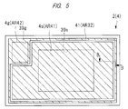
- FIG. 5 is a plan view of the configuration of the semiconductor chip in which the MOSFET is formed in the first embodiment.
- FIG. 6 is a cross-sectional view showing a principal part of the configuration of the semiconductor chip in which the MOSFET is formed in the first embodiment.
- FIG. 5 shows the state seen through a surface protection film 39 (see FIG. 6 ) for easy understanding.
- FIG. 6 is a cross-sectional view taken along the line B-B of FIG. 5 .
- a vertical MOSFET formed on a silicon (Si) substrate is taken as an example of the MOSFET 4.
- the MOSFET 4, that is, the semiconductor chip 2 includes an n + type semiconductor substrate 31, an n - type drift layer 32, an n + type source layer 33, a p type body layer 34 and a trench gate electrode 4tg in addition to the gate electrode 4g, the source electrode 4s and the drain electrode 4d described above.
- the n + type semiconductor substrate 31 is a semiconductor substrate made of Si
- the n - type drift layer 32, the n + type source layer 33 and the p type body layer 34 are semiconductor regions made of, for example, Si.
- the MOSFET 4 includes a semiconductor substrate made of Si and semiconductor regions made of Si formed in the semiconductor substrate.
- the semiconductor chip 2 includes the n + type semiconductor substrate 31 and the MOSFET 4 formed on the n + type semiconductor substrate 31.
- the n + type semiconductor substrate 31 is a semiconductor region to be the drain region of the MOSFET 4.
- the n + type semiconductor substrate 31 has a cell formation region AR41 on the side of a main surface 31a and a peripheral region AR42 on the side of the main surface 31a.
- the cell formation region AR41 is a region in which the MOSFET 4 is formed.
- the peripheral region AR42 is disposed on the peripheral side of the n + type semiconductor substrate 31 relative to the cell formation region AR41.
- the n- type drift layer 32 with an impurity concentration lower than that of the n + type semiconductor substrate 31 is formed on the main surface 31a of the n + type semiconductor substrate 31 in the cell formation region AR41 and the peripheral region AR42.
- the p type body layer 34 is formed in an upper layer part of the n - type drift layer 32.
- the p type body layer 34 is a semiconductor region to be the channel region of the MOSFET 4.
- the n + type source layer 33 with an impurity concentration higher than that of the n - type drift layer 32 is formed in an upper layer part of the p type body layer 34.
- the n + type source layer 33 is a semiconductor region to be the source region of the MOSFET 4.
- a trench 35 which passes through the n + type source layer 33 and the p type body layer 34 to reach the ri type drift layer 32 is formed in the n + type source layer 33 and the p type body layer 34.
- an insulating film 36 made of, for example, a silicon oxide film is formed on an inner wall of the trench 35 and on the n + type source layer 33.
- a part of the insulating film 36 formed on the inner wall of the trench 35 is a gate insulating film.
- a conductive film 37 made of, for example, a polycrystalline silicon film to which an impurity is introduced by ion implantation is formed on the insulating film 36.
- the trench gate electrode 4tg made of the conductive film 37 embedded in the trench 35 is formed on the insulating film 36 in the trench 35.
- the insulating film 36 is formed on the n- type drift layer 32 and the p type body layer 34, the conductive film 37 is formed on the insulating film 36, and a guard ring layer 37g made of the conductive film 37 formed on the insulating film 36 is formed.
- an interlayer insulating film 38 is formed on the n- type drift layer 32, the n + type source layer 33 and the p type body layer 34 so as to cover the insulating film 36 and the conductive film 37.
- the interlayer insulating film 38 is made of, for example, a silicon oxide film. Note that, in the cell formation region AR41, the interlayer insulating film 38 is formed on the n + type source layer 33 so as to cover the insulating film 36 and the trench gate electrode 4tg. Meanwhile, in the peripheral region AR42, the interlayer insulating film 38 is formed on the n - type drift layer 32 and the p type body layer 34 so as to cover the insulating film 36 and the guard ring layer 37g.
- a contact hole 38s which passes through the interlayer insulating film 38 and the n + type source layer 33 to reach the p type body layer 34 is formed in the interlayer insulating film 38.
- the source electrode 4s is formed in the contact hole 38s and on the interlayer insulating film 38. Therefore, the n + type source layer 33 and the p type body layer 34 are electrically connected to the source electrode 4s through the contact hole 38s.
- the source electrode 4s is made of, for example, a metal film containing aluminum (Al) as a main component.
- a contact hole 38g which passes through the interlayer insulating film 38 to reach the guard ring layer 37g is formed in the interlayer insulating film 38.
- a guard ring wiring 4w in the same layer as the source electrode 4s is formed in the contact hole 38g and on the interlayer insulating film 38.
- the trench gate electrode 4tg is electrically connected to the guard ring wiring 4w and the guard ring wiring 4w is electrically connected to the gate electrode 4g. Therefore, the trench gate electrode 4tg is electrically connected to the gate electrode 4g through the guard ring layer 37g, the contact hole 38g and the guard ring wiring 4w.
- the guard ring wiring 4w is made of a metal film in the same layer as the source electrode 4s, for example, a metal film containing aluminum as a main component.
- the surface protection film 39 is formed on the interlayer insulating film 38 so as to cover the source electrode 4s and the guard ring wiring 4w.
- an opening 39s (see FIG. 5 ) which passes through the surface protection film 39 to reach the source electrode 4s is formed in the surface protection film 39, and a source pad is formed of the source electrode 4s exposed at the bottom of the opening 39s.
- an opening 39g (see FIG. 5 ) which passes through the surface protection film 39 to reach the gate electrode 4g is formed, and a gate pad is formed of the gate electrode 4g exposed at the bottom of the opening 39g.
- the drain electrode 4d is formed on a rear surface 31b of the n + type semiconductor substrate 31.
- the drain electrode 4d is made of, for example, a conductive film containing nickel silicide as a main component.
- the MOSFET 4 in the first embodiment is a switching element serving as a three-terminal element having the source electrode 4s and the gate electrode 4g provided on the side of the main surface 31a of the n + type semiconductor substrate 31 and the drain electrode 4d provided on the side of the rear surface 31b of the n + type semiconductor substrate 31.
- FIG. 7 is a circuit block diagram showing an example of an electronic system in which the semiconductor device of the first embodiment is used.
- the electronic system in which the semiconductor device of the first embodiment is used includes a load such as a motor MOT as an AC motor, an inverter INV, a PFC (Power Factor Correction) circuit PC, a capacitor element CD, a converter CNV, a power source PS, a control circuit CTC and a gate driver DRV.
- a load such as a motor MOT as an AC motor, an inverter INV, a PFC (Power Factor Correction) circuit PC, a capacitor element CD, a converter CNV, a power source PS, a control circuit CTC and a gate driver DRV.
- the electronic system like this is, for example, an air-conditioning system such as an air conditioner.
- a three-phase motor is used as the motor MOT.
- the three-phase motor is configured to be driven by three-phase voltages each having different phases.
- the power source PS is connected to the inverter INV through the converter CNV, the PFC circuit PC and the capacitor element CD, and the DC voltage of the inverter CNV, that is, the DC power is supplied to the inverter INV. Since the converter CNV is interposed between the power source PS and the inverter INV, the AC voltage of the power source PS is converted to the DC voltage suitable for the motor drive and is then supplied to the inverter INV.
- the PFC circuit PC includes an inductor 41, an FRD (Fast Recovery Diode) 42, an IGBT (Insulated Gate Bipolar Transistor) 43 and a PFC-IC (Integrated circuit) 44, and is a circuit to bring the power factor of the power source close to 1.
- the control circuit CTC is connected to the inverter INV through the gate driver DRV, and the gate driver DRV is controlled based on the control signal from the control circuit CTC and the inverter INV is controlled by the control signal from the gate driver DRV.
- the DC voltage that is, the DC power is supplied to the inverter INV from the power source PS through the converter CNV and the PFC circuit PC.
- the supplied DC voltage that is, the DC power is converted into the AC voltage, that is, the AC power by the inverter INV controlled by the control circuit CTC and the gate driver DRV, and is supplied to the motor MOT, thereby driving the motor MOT.
- the control circuit CTC incorporates a control semiconductor chip such as an MCU (Micro Controller Unit).
- MCU Micro Controller Unit
- the motor MOT is a motor or a fan motor installed in a compressor of an outdoor unit of an air conditioner.
- an intelligent power module MOD1 is formed of the inverter INV and the gate driver DRV.
- a power module MOD2 is formed of the inverter INV.
- the motor MOT is a three-phase motor having a U phase PH1, a V phase PH2 and a W phase PH3.
- the inverter INV is configured to correspond to the three phases of the U phase PH1, the V phase PH2 and the W phase PH3.
- the inverter INV configured to correspond to the three phases has a total of six switching elements SW each including the semiconductor device of the first embodiment.
- the electronic system is provided with a plurality of switching elements SW, each of the plurality of switching elements SW includes the junction FET 3 (see FIG. 1 ) and the MOSFET 4 (see FIG. 1 ), and these switching elements SW constitute the inverter INV. Then, the motor MOT is driven by the inverter INV.
- the inverter INV has a total of four switching elements SW each including the semiconductor device of the first embodiment.
- the side close to the power source potential VDD relative to the input potential of the motor MOT is referred to as a high side.
- the side close to the ground potential GND relative to the input potential of the motor MOT is referred to as a low side.
- three switching elements SW1 are used as the switching elements SW on the high side, and three switching elements SW2 are used as the switching elements SW on the low side.
- the terminal D is electrically connected to the terminal P
- the terminal S is connected to any one of the terminals U, V and W serving as an output terminal to the motor MOT
- the terminal G is electrically connected to the gate driver DRV.
- the terminal D is connected to any one of the terminals U, V and W serving as an output terminal to the motor MOT
- the terminal S is electrically connected to the terminal N
- the terminal G is electrically connected to the gate driver DRV.
- the gate driver DRV drives the switching elements SW1 and SW2 so that the on-state or the off-state of the switching element SW1 on the high side and the on-state or the off-state of the switching element SW2 on the low side are alternately switched at each of the U phase PH1, the V phase PH2 and the W phase PH3.
- the inverter INV generates the AC voltage from the DC voltage and converts the DC power to the AC power.
- the motor MOT is driven by the AC power.
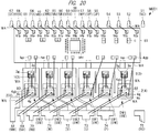
- FIG. 8 is a circuit block diagram showing an example of an intelligent power module in which the semiconductor device of the first embodiment is used.
- FIG. 9 is a top view schematically showing an example of the intelligent power module in which the semiconductor device of the first embodiment is used. Note that FIG. 9 shows the state seen through a sealing resin.
- the intelligent power module in which the semiconductor device of the first embodiment is used is formed of the inverter INV and the gate driver DRV shown in FIG. 7 .
- the intelligent power module MOD1 has a driver block DB1 and the inverter INV.
- the driver block DB1 includes the gate driver DRV.
- the inverter INV includes the three switching elements SW1 on the high side and the three switching elements SW2 on the low side like the inverter INV shown in FIG. 7 .
- the intelligent power module MOD1 has terminals 51 to 75.
- each of the terminals 51 and 75 is a terminal NC which is not connected to the outside.
- the terminal 55 is a terminal UP to which the control signal to control the switching element SW1 at the U phase on the high side is input.
- the terminal 56 is a terminal VP to which the control signal to control the switching element SW1 at the V phase on the high side is input.
- the terminal 57 is a terminal WP to which the control signal to control the switching element SW1 at the W phase on the high side is input.
- the terminals 58 and 63 are terminals VDD1 to which the power source potential is input.
- the terminals 59 and 66 are terminals VSS connected to the ground potential.
- the terminal 60 is a terminal UN to which the control signal to control the switching element SW2 at the U phase on the low side is input.
- the terminal 61 is a terminal VN to which the control signal to control the switching element SW2 at the V phase on the low side is input.
- the terminal 62 is a terminal WN to which the control signal to control the switching element SW2 at the W phase on the low side is input.
- the terminal 64 is an error output terminal FO.
- the terminal 67 is an overheat protection terminal OT.
- the terminal 74 is a terminal P to which the power source potential VDD of the inverter INV is input.
- the terminal 73 is a terminal U from which the U phase is output
- the terminal 72 is a terminal V from which the V phase is output
- the terminal 71 is a terminal W from which the W phase is output.
- the terminal 70 is a terminal NU at which the U phase is connected to the ground potential
- the terminal 69 is a terminal NV at which the V phase is connected to the ground potential
- the terminal 68 is a terminal NW at which the W phase is connected to the ground potential.
- the intelligent power module MOD1 has a wiring board 81 and an insulating plate 82 as shown in FIG. 9 .
- Pads 52p to 67p are formed on the wiring board 81, and the pads 52p to 67p are respectively connected to the terminals 52 to 67 by bonding wires WA.
- the chip 7 including the resistor R2 in each switching element SW, the chip 8 including the diode DI1 in each switching element SW, and the chip 9 including the resistor R1 in each switching element SW are mounted on the wiring board 81.
- the semiconductor chip 1 (junction FET 3) included in each of the three switching elements SW1 on the high side is mounted on the terminal 74 serving as a lead, and the semiconductor chip 2 (MOSFET 4) included in each of the three switching elements SW1 on the high side is mounted on the terminal 74 via the insulating plate 82.
- the semiconductor chip 1 (junction FET 3) included in the switching element SW2 at the U phase on the low side is mounted on the terminal 73 serving as a lead, and the semiconductor chip 2 included in the switching element SW2 at the U phase on the low side is mounted on the terminal 73 via the insulating plate 82.
- the semiconductor chip 1 (junction FET 3) included in the switching element SW2 at the V phase on the low side is mounted on the terminal 72 serving as a lead, and the semiconductor chip 2 included in the switching element SW2 at the V phase on the low side is mounted on the terminal 72 via the insulating plate 82.
- the semiconductor chip 1 (junction FET 3) included in the switching element SW2 at the W phase on the low side is mounted on the terminal 71 serving as a lead, and the semiconductor chip 2 included in the switching element SW2 at the W phase on the low side is mounted on the terminal 71 via the insulating plate 82.
- the gate electrode 3g of the semiconductor chip 1 (junction FET 3) is electrically connected to the pad 3gp formed on the wiring board 81 through the bonding wire WA.
- the source electrode 3s of the semiconductor chip 1 is electrically connected to the drain electrode 4d (see FIG. 6 ) of the semiconductor chip 2 (MOSFET 4) through the bonding wire WA and the insulating plate 82. Also, in each of the six switching elements SW, the gate electrode 4g of the semiconductor chip 2 is electrically connected to the pad 4gp formed on the wiring board 81 through the bonding wire WA.
- the drain electrode 3d (see FIG. 4 ) of the semiconductor chip 1 included in each of the three switching elements SW1 on the high side is electrically connected to the terminal 74.
- the drain electrode 3d (see FIG. 4 ) of the semiconductor chip 1 included in the switching element SW2 at the U phase on the low side is electrically connected to the terminal 73.
- the drain electrode 3d (see FIG. 4 ) of the semiconductor chip 1 included in the switching element SW2 at the V phase on the low side is electrically connected to the terminal 72.
- the drain electrode 3d (see FIG. 4 ) of the semiconductor chip 1 included in the switching element SW2 at the W phase on the low side is electrically connected to the terminal 71.
- the source electrode 4s of the semiconductor chip 2 included in the switching element SW1 at the U phase on the high side is electrically connected to the terminal 73 through the bonding wire WA.
- the source electrode 4s of the semiconductor chip 2 included in the switching element SW1 at the V phase on the high side is electrically connected to the terminal 72 through the bonding wire WA.
- the source electrode 4s of the semiconductor chip 2 included in the switching element SW1 at the W phase on the high side is electrically connected to the terminal 71 through the bonding wire WA.
- the source electrode 4s of the semiconductor chip 2 included in the switching element SW2 at the U phase on the low side is electrically connected to the terminal 70 through the bonding wire WA.
- the source electrode 4s of the semiconductor chip 2 included in the switching element SW2 at the V phase on the low side is electrically connected to the terminal 69 through the bonding wire WA.
- the source electrode 4s of the semiconductor chip 2 included in the switching element SW2 at the W phase on the low side is electrically connected to the terminal 68 through the bonding wire WA.
- the inverter INV and the gate driver DRV can be integrated and the size reduction can be achieved.
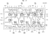
- FIG. 10 and FIG. 11 are top views schematically showing an example of a power module in which the semiconductor device of the first embodiment is used. Note that FIG. 10 and FIG. 11 show the state seen through a sealing resin.
- the power module MOD2 in which the semiconductor device of the first embodiment is used is formed of the inverter INV shown in FIG. 7 .
- the power module MOD2 has the inverter INV.
- the inverter INV includes the three switching elements SW1 on the high side and the three switching elements SW2 on the low side like the inverter INV shown in FIG. 7 .
- the power module MOD2 has a wiring board 83 and an insulating plate 84 in addition to the inverter INV as shown in FIG. 10 .
- the wiring board 83 has six terminals G serving as gate pads, six terminals S serving as source pads, terminals 68 to 74, three terminals 83ch serving as connection pads, and a terminal 83c1 serving as a connection pad.
- three terminals S correspond to the terminals 70, 69 and 68, respectively.
- the terminal 74 is a terminal P to which the power source potential VDD of the inverter INV is input like the terminal 74 shown in FIG. 8 .
- the terminal 73 is a terminal U from which the U phase is output like the terminal 73 shown in FIG. 8
- the terminal 72 is a terminal V from which the V phase is output like the terminal 72 shown in FIG. 8
- the terminal 71 is a terminal W from which the W phase is output like the terminal 71 shown in FIG. 8
- the terminal 70 is a terminal NU at which the U phase is connected to the ground potential like the terminal 70 shown in FIG. 8
- the terminal 69 is a terminal NV at which the V phase is connected to the ground potential like the terminal 69 shown in FIG. 8
- the terminal 68 is a terminal NW at which the W phase is connected to the ground potential like the terminal 68 shown in FIG. 8 .
- the semiconductor chip 1 (junction FET 3) included in each of the three switching elements SW1 on the high side is mounted on the terminal 74, and the semiconductor chip 2 (MOSFET 4) included in each of the three switching elements SW1 on the high side is mounted on the terminal 74 via the insulating plate 84.
- the semiconductor chip 1 included in the switching element SW2 at the U phase on the low side is mounted on the terminal 73, and the semiconductor chip 2 included in the switching element SW2 at the U phase on the low side is mounted on the terminal 73 via the insulating plate 84.
- the semiconductor chip 1 included in the switching element SW2 at the V phase on the low side is mounted on the terminal 72, and the semiconductor chip 2 included in the switching element SW2 at the V phase on the low side is mounted on the terminal 72 via the insulating plate 84.
- the semiconductor chip 1 included in the switching element SW2 at the W phase on the low side is mounted on the terminal 71, and the semiconductor chip 2 included in the switching element SW2 at the W phase on the low side is mounted on the terminal 71 via the insulating plate 84.
- the gate electrode 3g of the semiconductor chip 1 (junction FET 3) is electrically connected to the terminal G through the bonding wire WA, the terminal 83ch and the resistor R2 (chip 7). Also, in each of the three switching elements SW1 on the high side, the gate electrode 3g of the semiconductor chip 1 is electrically connected to the terminal S through the bonding wire WA, the terminal 83ch and the diode DI1 (chip 8).
- the gate electrode 3g of the semiconductor chip 1 (junction FET 3) is electrically connected to the terminal G through the bonding wire WA, the terminal 83c1 and the resistor R2 (chip 7). Also, in each of the three switching elements SW2 on the low side, the gate electrode 3g of the semiconductor chip 1 is electrically connected to the terminal S through the bonding wire WA, the terminal 83c1 and the diode DI1 (chip 8).
- the source electrode 3s of the semiconductor chip 1 is electrically connected to the drain electrode 4d (see FIG. 6 ) of the semiconductor chip 2 (MOSFET 4) through the bonding wire WA and the insulating plate 84. Also, in each of the six switching elements SW, the gate electrode 4g of the semiconductor chip 2 is electrically connected to the terminal G through the bonding wire WA.
- the drain electrode 3d (see FIG. 4 ) of the semiconductor chip 1 included in each of the three switching elements SW1 on the high side is electrically connected to the terminal 74.
- the drain electrode 3d (see FIG. 4 ) of the semiconductor chip 1 included in the switching element SW2 at the U phase on the low side is electrically connected to the terminal 73.
- the drain electrode 3d (see FIG. 4 ) of the semiconductor chip 1 included in the switching element SW2 at the V phase on the low side is electrically connected to the terminal 72.
- the drain electrode 3d (see FIG. 4 ) of the semiconductor chip 1 included in the switching element SW2 at the W phase on the low side is electrically connected to the terminal 71.
- the source electrode 4s of the semiconductor chip 2 included in each of the three switching elements SW1 on the high side is electrically connected to the terminal S through the bonding wire WA.
- the source electrode 4s of the semiconductor chip 2 included in the switching element SW2 at the U phase on the low side is electrically connected to the terminal 70 through the bonding wire WA.
- the source electrode 4s of the semiconductor chip 2 included in the switching element SW2 at the V phase on the low side is electrically connected to the terminal 69 through the bonding wire WA.
- the source electrode 4s of the semiconductor chip 2 included in the switching element SW2 at the W phase on the low side is electrically connected to the terminal 68 through the bonding wire WA.
- the inverter INV can be integrated and the size reduction can be achieved.
- three terminals 84a which are electrically insulated from the terminal 74 and on which the semiconductor chip 2 of each of the three switching elements SW1 on the high side is mounted may be provided instead of the insulating plate 84 (see FIG. 10 ).
- three terminals 84a which are electrically insulated from the terminals 73, 72 and 71 and on which the semiconductor chip 2 of each of the three switching elements SW2 on the low side is mounted may be provided instead of the insulating plate 84 (see FIG. 10 ).
- a thermistor 85 may be provided on the wiring board 83.
- FIG. 12 is a circuit diagram of a configuration of the semiconductor device of the comparative example.
- FIG. 13 is a cross-sectional view showing a principal part of a configuration of a semiconductor chip in which a junction FET is formed in the comparative example. Note that the configuration of the semiconductor chip in the comparative example shown in FIG. 13 is the same as the configuration of the semiconductor chip in the first embodiment shown in FIG. 4 . Also, the flow of electrons in the junction FET 3 when the switching element is in an on-state is indicated by arrows E101 in FIG. 13 .
- the semiconductor device of the comparative example also has the semiconductor chip 1, the semiconductor chip 2, the terminal G and the terminal D like the semiconductor device of the first embodiment.
- the normally-on junction FET 3 is formed in the semiconductor chip 1
- the normally-off MOSFET 4 is formed in the semiconductor chip 2.
- the junction FET 3 and the MOSFET 4 are connected in series between the terminal D and the ground potential like the semiconductor device of the first embodiment.
- the semiconductor device of the comparative example also has the junction FET 3 and the MOSFET 4 in cascode connection between the terminal D and the ground potential like the semiconductor device of the first embodiment.
- the gate electrode 3g of the junction FET 3 is not electrically connected to the gate electrode 4g of the MOSFET 4 and is electrically connected to the source electrode 4s of the MOSFET 4 unlike in the first embodiment. Also, in the example shown in FIG. 12 , the gate electrode 3g of the junction FET 3 is grounded.
- the potential of the gate electrode 3g of the junction FET 3 is the ground potential, that is, 0 V. Since the junction FET 3 is a normally-on junction FET, it is in an on-state when the voltage applied to the gate electrode 3g is 0 V. Also, when the junction FET 3 is in an on-state, electrons as charge carriers flow in the junction FET 3 from the n + type source layer 13 to the n + type semiconductor substrate 11 as the drain region through a part of the n - type drift layer 12 located between the adjacent p type gate layers 14 as indicated by the arrow E101.
- a depletion layer DL is likely to be formed in the part of the n - type drift layer 12 adjacent to the p type gate layer 14 in the junction FET 3 as shown in FIG. 13 .
- An interval between the adjacent two p type gate layers 14 may be widened in order to reduce the on-resistance described above.
- the withstand voltage of the junction FET 3 is decreased.
- the semiconductor device of the comparative example has the junction FET and the MOSFET 4 in cascode connection between the terminal D and the ground potential like the semiconductor device of the first embodiment. Therefore, when the on-resistance of the junction FET 3 in cascode connection with the MOSFET 4 is increased, the overall on-resistance of the semiconductor device is increased.
- the MOSFET 4 includes the semiconductor region made of Si and the junction FET 3 includes the semiconductor region made of, for example, SiC which is semiconductor with a band gap larger than that of Si like in the first embodiment.
- the withstand voltage of the junction FET 3 is higher than the withstand voltage of the MOSFET 4.
- the withstand voltage of the junction FET 3 is set to be about ten times as high as the withstand voltage of the MOSFET 4. Accordingly, when the withstand voltage of the junction FET 3 with the withstand voltage higher than the withstand voltage of the MOSFET 4 in the cascode-connected junction FET 3 and MOSFET 4 is decreased, the overall withstand voltage of the semiconductor device is decreased.
- the gate electrode 3g of the junction FET 3 is connected to the source electrode 4s of the MOSFET 4, and thus it is difficult to achieve both of the improvement of the withstand voltage and the reduction of the on-resistance.
- the gate electrode 3g of the junction FET 3 is electrically connected to the gate electrode 4g of the MOSFET 4.
- the potential of the gate electrode 3g of the junction FET 3 is not the ground potential, that is, 0 V, and a positive voltage is applied to the gate electrode 3g of the junction FET 3.
- the depletion layer DL is less likely to be formed in the part of the n - type drift layer 12 adjacent to the p type gate layer 14 in the junction FET 3.
- the MOSFET 4 including the semiconductor region made of Si and the junction FET 3 including the semiconductor region made of SiC which is semiconductor with a band gap larger than that of Si are cascode-connected.
- the junction FET 3 has the withstand voltage higher than that of the MOSFET 4. Therefore, in the first embodiment, it is possible to achieve both of the improvement of the withstand voltage of the semiconductor device and the reduction of the on-resistance of the semiconductor device by improving the withstand voltage of the junction FET 3 and reducing the on-resistance of the junction FET 3.
- the fact that the source width for securing a certain amount of withstand voltage can be narrowed means that a predetermined withstand voltage can be secured even if the dimensional accuracy of the source width is not increased so much. Accordingly, it is possible to improve the yield in the manufacturing process and reduce the manufacturing cost of the semiconductor device.
- the current density of the junction FET 3 by reducing the on-resistance. Accordingly, it is possible to reduce the chip size (chip area) for securing the desired current amount, and the size reduction of the semiconductor device can be achieved. In addition, as a result of the reduction of the chip size, the number of chips manufactured by dividing one wafer is increased, so that the manufacturing cost of the semiconductor device can be reduced.
- the originally-possessed advantage in the manufacturing cost can be enhanced when the junction FET and the MOSFET in cascode connection are used as the semiconductor device in comparison with the case in which other power transistors such as IGBT are used as the semiconductor device.
- the gate electrode 3g of the junction FET 3 is electrically connected to the gate electrode 4g of the MOSFET 4 through the voltage control element 6.
- the voltage control element 6 includes, for example, the resistor R2 and the diode DI1, and the gate electrode 3g of the junction FET 3 is electrically connected to the gate electrode 4g of the MOSFET 4 through the resistor R2 and is grounded through the diode DI1, or is electrically connected to the source electrode 4s of the MOSFET 4.
- the on-resistance of the junction FET 3 can be reduced by about 30% in comparison with the case in which the voltage of about 0 V is applied to the gate electrode 3g of the junction FET 3.
- the voltage control element 6 includes the resistor R2 and the diode DI1, and the gate electrode 3g of the junction FET 3 is grounded through the diode DI1 or is electrically connected to the source electrode 4s of the MOSFET 4. Meanwhile, the voltage control element 6 may include only the resistor R2 but not include the diode DI1.
- the semiconductor device of the first modification example of the first embodiment Note that the differences from the semiconductor device of the first embodiment will be mainly described below.
- FIG. 14 is a circuit diagram of a configuration of the semiconductor device of the first modification example of the first embodiment.
- the voltage control element 6, that is, the voltage applying unit 6a includes the resistor R2 but does not include the diode DI1 (see FIG. 1 ).
- the gate electrode 3g of the junction FET 3 is electrically connected to the terminal G through the resistor R2. Namely, the gate electrode 3g of the junction FET 3 is electrically connected to the gate electrode 4g of the MOSFET 4 through the resistor R2.
- the depletion layer DL (see FIG. 13 ) is not formed in the part of the n - type drift layer 12 adjacent to the p type gate layer 14 in the junction FET 3 as shown in FIG. 4 .
- the withstand voltage of the junction FET 3 is not decreased like in the first embodiment. Therefore, it is possible to achieve both of the improvement of the withstand voltage and the reduction of the on-resistance also in the semiconductor device of the first modification example like the semiconductor device of the first embodiment.
- the voltage control element 6 includes the resistor R2 but does not include the diode DI1 (see FIG. 1 ) in the first modification example, the configuration of the voltage control element 6 can be simplified in comparison with the first embodiment.
- the semiconductor device of the first embodiment is more preferable in comparison with the semiconductor device of the first modification example in that there is no fear that the pn diode is brought into an on-state and there is no fear of the conduction deterioration due to the stacking fault in SiC or the like.
- the gate electrode 3g of the junction FET 3 is electrically connected to the gate electrode 4g of the MOSFET 4. Meanwhile, it is only required to apply a voltage with a polarity opposite to that of the voltage applied to the gate electrode 3g of the junction FET 3 to bring the junction FET 3 into an off-state, to the gate electrode 3g of the junction FET 3 when the MOSFET 4 is in an on-state.
- the case like this will be described as the semiconductor device of the second modification example of the first embodiment. Note that the differences from the semiconductor device of the first embodiment will be mainly described below.
- FIG. 15 is a circuit diagram of a configuration of the semiconductor device of the second modification example of the first embodiment.
- the voltage control element 6 does not have to be electrically connected to the terminal G, that is, the gate electrode 4g of the MOSFET 4, and may be connected to, for example, a terminal which is not directly electrically connected to the terminal G.
- the voltage control element 6 is the voltage applying unit 6a which applies the voltage to the gate electrode 3g of the junction FET 3.
- the voltage applying unit 6a applies a voltage with a polarity opposite to that of the voltage applied to the gate electrode 3g of the junction FET 3 to bring the junction FET 3 into an off-state, to the gate electrode 3g of the junction FET 3 when the MOSFET 4 is in an on-state.
- the voltage applying unit 6a applies a voltage with a polarity opposite to that of the voltage applied to the gate electrode 3g of the junction FET 3 when the junction FET 3 is brought into an off-state, to the gate electrode 3g of the junction FET 3 when the MOSFET 4 is in an on-state.
- the polarity of the voltage applied to the gate electrode 3g of the junction FET when the junction FET 3 is brought into an off-state is negative.
- Examples of the voltage control element 6 as the voltage applying unit 6a described above include a voltage applying circuit which applies a voltage with the same polarity as that of the voltage applied to the gate electrode 4g of the MOSFET 4, to the gate electrode 3g of the junction FET 3 in synchronization with, for example, the voltage applied to the terminal G when the MOSFET 4 is in an on-state.
- a variety of voltage applying circuits and voltage control elements can also be used other than that.
- the depletion layer DL (see FIG. 13 ) is not formed in the part of the n - type drift layer 12 adjacent to the p type gate layer 14 when the junction FET 3 is in an on-state like in the first embodiment. Accordingly, it is not necessary to widen the interval between the two adjacent p type gate layers 14 in order to reduce the on-resistance of the junction FET 3, and thus the withstand voltage of the junction FET 3 is not decreased. Therefore, it is possible to achieve both of the improvement of the withstand voltage and the reduction of the on-resistance also in the semiconductor device of the second modification example like the semiconductor device of the first embodiment.
- the voltage control element 6 includes one diode and the gate electrode 3g of the junction FET 3 is grounded through the diode or electrically connected to the source electrode 4s of the MOSFET 4. Meanwhile, the voltage control element 6 may include two diodes. The case like this will be described as the semiconductor device of the second embodiment. Note that the differences from the semiconductor device of the first embodiment will be mainly described below.
- FIG. 16 is a circuit diagram of a configuration of the semiconductor device of the second embodiment.
- the voltage control element 6 includes, for example, the resistor R2, the diode DI1 and a diode DI2.
- the gate electrode 3g of the junction FET 3 is electrically connected to the terminal G through the resistor R2. Namely, the gate electrode 3g of the junction FET 3 is electrically connected to the gate electrode 4g of the MOSFET 4 through the resistor R2.
- An anode 8a of the diode DI1 is electrically connected to one end of the resistor R2 on the side of the gate electrode 3g through the diode DI2, and an anode 8sa of the diode DI2 is electrically connected to one end of the resistor R2 on the side of the gate electrode 3g.
- a cathode 8sc of the diode DI2 is electrically connected to the anode 8a of the diode DI1, and a cathode 8c of the diode DI1 is grounded.
- a plurality of diodes including the diodes DI1 and DI2 are connected in series between the one end of the resistor R2 on the side of the gate electrode 3g and the ground potential.
- the diode DI2 has a pn junction made of, for example, a p type silicon and an n type silicon like the diode DI1.
- a cathode 8c of the diode DI1 does not have to be grounded or may be electrically connected to the source electrode 4s of the MOSFET 4 as described above with reference to FIG. 1 and FIG. 2 .
- the on-resistance of the junction FET 3 can be made lower than the on-resistance of the junction FET 3 in the first embodiment, and the stable control thereof can be achieved.
- the depletion layer DL (see FIG. 13 ) is less likely to be formed in the part of the n - type drift layer 12 adjacent to the p type gate layer 14 when the junction FET 3 is in an on-state in comparison with the first embodiment. Therefore, it is not necessary to widen the interval between the two adjacent p type gate layers 14 in order to reduce the on-resistance of the junction FET 3, and thus the withstand voltage of the junction FET 3 is much less likely to be decreased. Accordingly, it is possible to achieve both of the further improvement of the withstand voltage and the further reduction of the on-resistance in the semiconductor device of the second embodiment in comparison with the semiconductor device of the first embodiment.
- the MOSFET 4 when the MOSFET 4 is in an off-state, for example, by applying the voltage of 0 V to the gate electrode 4g of the MOSFET 4, the voltage of 0 V is applied also to the gate electrode 3g of the junction FET 3 like in the first embodiment.
- the number of diodes included in the voltage control element 6 is not limited to two. Namely, the number of diodes connected in series between one end of the resistor R2 on the side of the gate electrode 3g and the ground potential may be three or more. By adjusting the number of diodes connected in series between one end of the resistor R2 on the side of the gate electrode 3g and the ground potential, the voltage applied to the gate electrode 3g of the junction FET 3 when the MOSFET 4 is brought into an on-state can be freely adjusted to be several times as high as the internal potential.
- the semiconductor device includes the chip 7 and the chip 8, and the chip 7 includes the resistor R2 and the chip 8 includes the diode DI1.
- the semiconductor chip 2 including the MOSFET 4 may include the resistor R2 and the diode DI1.
- the MOSFET 4, the resistor R2 and the diode DI1 may be formed in the same semiconductor chip 2. The case like this will be described as the semiconductor device of the third embodiment. Note that the differences from the semiconductor device of the first embodiment will be mainly described below.
- FIG. 17 is a circuit diagram of a configuration of a semiconductor device of the third embodiment.
- the semiconductor device of the third embodiment can be configured in the same manner as that of the first embodiment except that the MOSFET 4, the resistor R2 and the diode DI1 are formed in the same semiconductor chip 2.
- the voltage control element 6 includes the resistor R2 and the diode DI1 like in the first embodiment.
- the gate electrode 3g of the junction FET 3 is electrically connected to the terminal G through the resistor R2.
- the gate electrode 3g of the junction FET 3 is electrically connected to the gate electrode 4g of the MOSFET 4 through the resistor R2.
- the semiconductor device of the third embodiment does not have the chip 7 (see FIG. 1 ) and the chip 8 (see FIG. 1 ) unlike the semiconductor device of the first embodiment.
- the MOSFET 4, the resistor R2 and the diode DI1 are formed in the semiconductor chip 2. Accordingly, as described later with reference to FIG. 18 to FIG. 22 , the number of parts to be mounted when assembling an intelligent power module or a power module can be reduced, and the manufacturing cost can be reduced. Further, the design of the arrangement of the terminals in the wiring board of the intelligent power module and the power module can be facilitated.
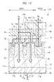
- FIG. 18 is a plan view of the configuration of the semiconductor chip in which the MOSFET is formed in the third embodiment.
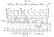
- FIG. 19 is a cross-sectional view showing a principal part of the configuration of the semiconductor chip in which the MOSFET is formed in the third embodiment.
- FIG. 18 shows the state seen through a surface protection film 39 (see FIG. 19 ) for easy understanding.
- FIG. 19 is a cross-sectional view taken along the line C-C of FIG. 18 .
- a vertical MOSFET formed on a silicon (Si) substrate is taken as an example of the MOSFET 4, and the differences from the semiconductor chip 2 described in the first embodiment with reference to FIG. 5 and FIG. 6 will be mainly described.
- the structure of the semiconductor chip 2 in the cell formation region AR41 in the third embodiment is the same as the structure of the semiconductor chip 2 in the cell formation region AR41 in the first embodiment described with reference to FIG. 5 and FIG. 6 , and thus the description thereof is omitted.
- the n + type semiconductor substrate 31 has a diode formation region AR43 on the side of the main surface 31a and a resistor formation region AR44 on the side of the main surface 31a in addition to the cell formation region AR41 on the side of the main surface 31a and the peripheral region AR42 on the side of the main surface 31a.
- the diode formation region AR43 is a region in which the diode DI1 is formed
- the resistor formation region AR44 is a region in which the resistor R2 is formed.
- the diode formation region AR43 and the resistor formation region AR44 are disposed on the peripheral side of the n + type semiconductor substrate 31 relative to the cell formation region AR41, and are disposed so as to be surrounded by, for example, the peripheral region AR42.
- the n - type drift layer 32 with an impurity concentration lower than that of the n + type semiconductor substrate 31 is formed on the main surface 31a of the n + type semiconductor substrate 31 like the peripheral region AR42.
- the insulating film 36 is formed on the n - type drift layer 32.
- a p type semiconductor region 37p made of, for example, a polycrystalline silicon film to which a p type impurity is introduced by ion implantation and an n type semiconductor region 37n made of, for example, a polycrystalline silicon film to which an n type impurity is introduced by ion implantation are formed on the insulating film 36 so as to be adjacent to each other.
- the diode DI1 is formed of the p type semiconductor region 37p and the n type semiconductor region 37n.
- a resistor film 37r made of, for example, a polycrystalline silicon film to which an impurity is introduced by ion implantation is formed on the insulating film 36.
- the resistor R2 is formed of the resistor film 37r.
- the semiconductor chip 2 includes the resistor R2 formed on the n + type semiconductor substrate 31 and the diode DI1 formed on the n + type semiconductor substrate 31.
- the interlayer insulating film 38 is formed on the n - type drift layer 32 so as to cover the insulating film 36, the p type semiconductor region 37p and the n type semiconductor region 37n.
- the interlayer insulating film 38 is formed on the n - type drift layer 32 so as to cover the insulating film 36 and the resistor film 37r.
- a contact hole 38p which passes through the interlayer insulating film 38 to reach the p type semiconductor region 37p and a contact hole 38n which passes through the interlayer insulating film 38 to reach the n type semiconductor region 37n are formed in the interlayer insulating film 38.
- contact holes 38r1 and 38r2 which pass through the interlayer insulating film 38 to reach the resistor film 37r are formed.
- the source electrode 4s is formed in the contact holes 38s and 38n and on the interlayer insulating film 38. Further, the source electrode 4s is electrically connected to the n type semiconductor region 37n through the contact hole 38n.
- the gate bias electrode 4gb is formed in the contact holes 38p and 38r2 and on the interlayer insulating film 38.
- the resistor film 37r is electrically connected to the p type semiconductor region 37p through the contact hole 38r2, the gate bias electrode 4gb and the contact hole 38p.
- the gate bias electrode 4gb is made of a metal film in the same layer as the source electrode 3s, for example, a metal film containing aluminum as a main component.
- the guard ring wiring 4w is formed in the contact holes 38g and 38r1 and on the interlayer insulating film 38.
- the guard ring wiring 4w is electrically connected to the resistor film 37r through the contact hole 38r1.
- the surface protection film 39 is formed on the interlayer insulating film 38 so as to cover the source electrode 4s, the gate bias electrode 4gb and the guard ring wiring 4w.
- an opening 39gb which passes through the surface protection film 39 to reach the gate bias electrode 4gb is formed in the surface protection film 39, and a gate bias pad is formed of the gate bias electrode 4gb exposed at the bottom of the opening 39gb.
- the MOSFET 4, the resistor R2 and the diode DI1 can be formed in the same semiconductor chip 2.
- FIG. 20 is a top view schematically showing an example of the intelligent power module in which the semiconductor device of the third embodiment is used.
- FIG. 20 shows the state seen through a sealing resin.
- the resistor R2 and the diode DI1 are formed in the semiconductor chip 2 as described with reference to FIG. 19 . Therefore, as shown in FIG. 20 , the chip 7 (see FIG. 9 ) including the resistor R2 and the chip 8 (see FIG. 9 ) including the diode DI1 are not mounted on the wiring board 81 in the intelligent power module MOD1 in the third embodiment unlike the intelligent power module MOD1 in the first embodiment described with reference to FIG. 9 .
- the gate electrode 3g of the semiconductor chip 1 (junction FET 3) is not connected to the pad 3gp formed on the wiring board 81, and is electrically connected to the gate bias electrode 4gb of the semiconductor chip 2 (MOSFET 4) through the bonding wire WA.
- the number of parts to be mounted when assembling an intelligent power module can be reduced, and the manufacturing cost can be reduced. Further, the design of the arrangement of the terminals in the wiring board of the intelligent power module can be facilitated.
- FIG. 20 shows the example in which the chip 9 (see FIG. 9 ) including the resistor R1 in each switching element SW is also not mounted on the wiring board 81 for the reason that it is formed in the semiconductor chip 2 or the like.
- FIG. 21 and FIG. 22 are top views schematically showing an example of a power module in which the semiconductor device of the third embodiment is used. Note that FIG. 21 and FIG. 22 show the state seen through a sealing resin. Also, the differences from the power module described in the first embodiment with reference to FIG. 10 and FIG. 11 will be mainly described below.
- the resistor R2 and the diode DI1 are formed in the semiconductor chip 2 as described with reference to FIG. 19 .
- the chip 7 (see FIG. 10 ) including the resistor R2 and the chip 8 (see FIG. 10 ) including the diode DI1 are not mounted on the wiring board 83 in the power module MOD2 in the third embodiment unlike the power module MOD2 in the first embodiment described with reference to FIG. 10 .
- the gate electrode 3g of the semiconductor chip 1 (junction FET 3) is not connected to the terminal 83ch, and is electrically connected to the gate bias electrode 4gb of the semiconductor chip 2 (MOSFET 4) through the bonding wire WA and an insulating plate 84b.
- the gate electrode 3g of the semiconductor chip 1 is not connected to the terminal 83cl, and is electrically connected to the gate bias electrode 4gb of the semiconductor chip 2 through the bonding wire WA and the insulating plate 84b.
- the number of parts to be mounted when assembling a power module can be reduced, and the manufacturing cost can be reduced. Further, the design of the arrangement of the terminals in the wiring board of the power module can be facilitated.
- three terminals 84a which are electrically insulated from the terminal 74 and on which the semiconductor chip 2 of each of the three switching elements SW1 on the high side is mounted may be provided instead of the insulating plates 84 and 84b (see FIG. 21 ).
- three terminals 84a which are electrically insulated from the terminals 73, 72 and 71 and on which the semiconductor chip 2 of each of the three switching elements SW2 on the low side is mounted may be provided instead of the insulating plates 84 and 84b (see FIG. 21 ).
- the semiconductor device of the third embodiment has the characteristics similar to those of the semiconductor device of the first embodiment, and thus exhibits the same effect as that of the semiconductor device of the first embodiment.
- the MOSFET 4, the resistor R2 and the diode DI1 are formed in the same semiconductor chip in the semiconductor device of the third embodiment unlike the semiconductor device of the first embodiment. Accordingly, the number of parts to be mounted when assembling an intelligent power module or a power module can be reduced, and the manufacturing cost can be reduced. Further, the design of the arrangement of the terminals in the wiring board of the intelligent power module and the power module can be facilitated.
Landscapes
- Engineering & Computer Science (AREA)
- Power Engineering (AREA)
- Metal-Oxide And Bipolar Metal-Oxide Semiconductor Integrated Circuits (AREA)
- Junction Field-Effect Transistors (AREA)
- Inverter Devices (AREA)
- Electrodes Of Semiconductors (AREA)
Applications Claiming Priority (1)
| Application Number | Priority Date | Filing Date | Title |
|---|---|---|---|
| JP2015087671A JP6509621B2 (ja) | 2015-04-22 | 2015-04-22 | 半導体装置 |
Publications (2)
| Publication Number | Publication Date |
|---|---|
| EP3086472A1 true EP3086472A1 (fr) | 2016-10-26 |
| EP3086472B1 EP3086472B1 (fr) | 2018-11-21 |
Family
ID=55750345
Family Applications (1)
| Application Number | Title | Priority Date | Filing Date |
|---|---|---|---|
| EP16164852.2A Not-in-force EP3086472B1 (fr) | 2015-04-22 | 2016-04-12 | Dispositif semi-conducteur |
Country Status (5)
| Country | Link |
|---|---|
| US (2) | US9837395B2 (fr) |
| EP (1) | EP3086472B1 (fr) |
| JP (1) | JP6509621B2 (fr) |
| CN (1) | CN106067794B (fr) |
| TW (1) | TW201709522A (fr) |
Cited By (2)
| Publication number | Priority date | Publication date | Assignee | Title |
|---|---|---|---|---|
| US20160086878A1 (en) * | 2014-09-23 | 2016-03-24 | Infineon Technologies Austria Ag | Electronic Component |
| WO2026041304A1 (fr) * | 2024-08-19 | 2026-02-26 | Sew-Eurodrive Gmbh & Co Kg | Agencement de circuit pouvant être commandé |
Families Citing this family (19)
| Publication number | Priority date | Publication date | Assignee | Title |
|---|---|---|---|---|
| US10277115B2 (en) | 2016-04-15 | 2019-04-30 | Emerson Climate Technologies, Inc. | Filtering systems and methods for voltage control |
| US10305373B2 (en) | 2016-04-15 | 2019-05-28 | Emerson Climate Technologies, Inc. | Input reference signal generation systems and methods |
| US10312798B2 (en) | 2016-04-15 | 2019-06-04 | Emerson Electric Co. | Power factor correction circuits and methods including partial power factor correction operation for boost and buck power converters |
| US10284132B2 (en) | 2016-04-15 | 2019-05-07 | Emerson Climate Technologies, Inc. | Driver for high-frequency switching voltage converters |
| US10763740B2 (en) | 2016-04-15 | 2020-09-01 | Emerson Climate Technologies, Inc. | Switch off time control systems and methods |
| US10656026B2 (en) | 2016-04-15 | 2020-05-19 | Emerson Climate Technologies, Inc. | Temperature sensing circuit for transmitting data across isolation barrier |
| US9933842B2 (en) | 2016-04-15 | 2018-04-03 | Emerson Climate Technologies, Inc. | Microcontroller architecture for power factor correction converter |
| CN106712749B (zh) * | 2016-11-14 | 2021-09-21 | 南京工程学院 | 基于碳化硅mosfet和jfet的混合高压器件 |
| CN107037852B (zh) * | 2017-06-06 | 2021-01-15 | 哈尔滨工业大学深圳研究生院 | 线性压控电流源拓扑结构及太阳阵模拟器 |
| JP6783708B2 (ja) * | 2017-06-15 | 2020-11-11 | ルネサスエレクトロニクス株式会社 | 半導体装置 |
| JP6769458B2 (ja) * | 2017-07-26 | 2020-10-14 | 株式会社デンソー | 半導体装置 |
| CN107483035A (zh) * | 2017-08-22 | 2017-12-15 | 广东美的制冷设备有限公司 | 开关器件、空调器的电控板以及空调器 |
| JP6619522B1 (ja) * | 2018-03-29 | 2019-12-11 | 新電元工業株式会社 | ワイドギャップ半導体装置 |
| US11322545B2 (en) * | 2018-04-27 | 2022-05-03 | Hewlett Packard Enterprise Development Lp | Vertical JFET device for memristor array interface |
| JP7024688B2 (ja) * | 2018-11-07 | 2022-02-24 | 株式会社デンソー | 半導体装置 |
| JP7316865B2 (ja) | 2019-07-22 | 2023-07-28 | ルネサスエレクトロニクス株式会社 | 半導体装置 |
| JP7524665B2 (ja) * | 2020-08-12 | 2024-07-30 | 富士電機株式会社 | 半導体装置 |
| US20260019073A1 (en) * | 2024-07-11 | 2026-01-15 | Semiconductor Components Industries, Llc | Cascode switching circuit |
| US20260039216A1 (en) * | 2024-07-31 | 2026-02-05 | BorgWarner US Technologies LLC | Systems and methods for electrical element for inverter for electric vehicle |
Citations (6)
| Publication number | Priority date | Publication date | Assignee | Title |
|---|---|---|---|---|
| JPH0512930B2 (fr) | 1985-06-28 | 1993-02-19 | Dasukin Kk | |
| US20010024138A1 (en) * | 1998-09-25 | 2001-09-27 | Karl-Otto Dohnke | Electronic switching device having at least two semiconductor components |
| DE102006029928B3 (de) * | 2006-06-29 | 2007-09-06 | Siemens Ag | Elektronische Schalteinrichtung mit zumindest zwei Halbleiterschaltelementen |
| JP2014003110A (ja) | 2012-06-18 | 2014-01-09 | Renesas Electronics Corp | 半導体装置及びそれを用いたシステム |
| US20140049296A1 (en) * | 2012-08-16 | 2014-02-20 | Samsung Electronics Co., Ltd. | Electronic device including transistor and method of operating the same |
| JP2014512765A (ja) | 2011-04-13 | 2014-05-22 | パワー・インテグレーションズ・インコーポレーテッド | ノーマリーオフ装置およびノーマリーオン装置を含むカスケードスイッチ並びに本スイッチを備える回路 |
Family Cites Families (36)
| Publication number | Priority date | Publication date | Assignee | Title |
|---|---|---|---|---|
| US4940906A (en) * | 1988-08-08 | 1990-07-10 | Zdzislaw Gulczynski | Power switch driver |
| US5534810A (en) * | 1994-12-28 | 1996-07-09 | Thomson Consumer Electronics, Inc. | Power stage bias circuit with improved efficiency and stability |
| US5761317A (en) * | 1996-03-04 | 1998-06-02 | Pritchard; Eric K. | Tube amplifier fat emulation structure |
| JP4122880B2 (ja) * | 2002-07-24 | 2008-07-23 | 住友電気工業株式会社 | 縦型接合型電界効果トランジスタ |
| CN101567373B (zh) * | 2004-02-16 | 2011-04-13 | 富士电机系统株式会社 | 双方向元件及其制造方法 |
| JP4489485B2 (ja) * | 2004-03-31 | 2010-06-23 | 株式会社ルネサステクノロジ | 半導体装置 |
| US7071770B2 (en) * | 2004-05-07 | 2006-07-04 | Micron Technology, Inc. | Low supply voltage bias circuit, semiconductor device, wafer and system including same, and method of generating a bias reference |
| US7019344B2 (en) * | 2004-06-03 | 2006-03-28 | Ranbir Singh | Lateral drift vertical metal-insulator semiconductor field effect transistor |
| US7105875B2 (en) * | 2004-06-03 | 2006-09-12 | Wide Bandgap, Llc | Lateral power diodes |
| US7205629B2 (en) * | 2004-06-03 | 2007-04-17 | Widebandgap Llc | Lateral super junction field effect transistor |
| US7202528B2 (en) * | 2004-12-01 | 2007-04-10 | Semisouth Laboratories, Inc. | Normally-off integrated JFET power switches in wide bandgap semiconductors and methods of making |
| US7715303B2 (en) * | 2005-09-27 | 2010-05-11 | Mediatek Incorporation | Recording apparatus for optical data |
| EP1935026A1 (fr) * | 2005-10-12 | 2008-06-25 | Acco | Transistor à effet de champ à grille isolé ayant une grille factice |
| US8017978B2 (en) * | 2006-03-10 | 2011-09-13 | International Rectifier Corporation | Hybrid semiconductor device |
| US7449762B1 (en) * | 2006-04-07 | 2008-11-11 | Wide Bandgap Llc | Lateral epitaxial GaN metal insulator semiconductor field effect transistor |
| US7888706B2 (en) * | 2006-05-31 | 2011-02-15 | Infineon Technologies Ag | High-efficiency filler cell with switchable, integrated buffer capacitance for high frequency applications |
| US7508225B2 (en) * | 2006-09-07 | 2009-03-24 | Kyocera Wireless Corporation | Apparatus, system and method for identification with temperature dependent resistive device |
| CA2591521A1 (fr) * | 2007-05-31 | 2008-11-30 | Ivan Meszlenyi | Convertisseur a transfert indirect et a large plage d'alimentation |
| JP2009207077A (ja) * | 2008-02-29 | 2009-09-10 | Denso Corp | 半導体集積回路装置 |
| FR2956212B1 (fr) * | 2010-02-08 | 2012-03-09 | Schneider Electric Ind Sas | Dispositif et procede de comptage d'energie electrique |
| JP5012930B2 (ja) | 2010-02-15 | 2012-08-29 | 株式会社デンソー | ハイブリッドパワーデバイス |
| JP5484138B2 (ja) * | 2010-03-12 | 2014-05-07 | ルネサスエレクトロニクス株式会社 | 電子回路装置 |
| DE102010027832B3 (de) * | 2010-04-15 | 2011-07-28 | Infineon Technologies AG, 85579 | Halbleiterschaltanordnung mit einem selbstleitenden und einem selbstsperrenden Transistor |
| WO2012023556A1 (fr) * | 2010-08-20 | 2012-02-23 | シャープ株式会社 | Inverseur |
| US8351243B2 (en) * | 2010-11-16 | 2013-01-08 | Sandisk 3D Llc | Transistor driven 3D memory |
| US8766375B2 (en) * | 2011-03-21 | 2014-07-01 | International Rectifier Corporation | Composite semiconductor device with active oscillation prevention |
| US9362905B2 (en) * | 2011-03-21 | 2016-06-07 | Infineon Technologies Americas Corp. | Composite semiconductor device with turn-on prevention control |
| JP5290354B2 (ja) * | 2011-05-06 | 2013-09-18 | シャープ株式会社 | 半導体装置および電子機器 |
| EP2693639B1 (fr) * | 2012-07-30 | 2015-09-09 | Nxp B.V. | Dispositifs à semi-conducteurs cascadés |
| CN203055909U (zh) * | 2012-11-28 | 2013-07-10 | 深圳市明微电子股份有限公司 | 一种合成结构的高压器件 |
| JP6073719B2 (ja) | 2013-03-21 | 2017-02-01 | ルネサスエレクトロニクス株式会社 | 半導体装置の製造方法および半導体装置 |
| JP6154705B2 (ja) * | 2013-09-24 | 2017-06-28 | 株式会社 日立パワーデバイス | 半導体スイッチ回路、信号処理装置、および、超音波診断装置 |
| US9472948B2 (en) * | 2013-09-30 | 2016-10-18 | Infineon Technologies Ag | On chip reverse polarity protection compliant with ISO and ESD requirements |
| JP2015173181A (ja) * | 2014-03-11 | 2015-10-01 | 古河電気工業株式会社 | 半導体装置 |
| US9400513B2 (en) * | 2014-06-30 | 2016-07-26 | Infineon Technologies Austria Ag | Cascode circuit |
| WO2016018610A1 (fr) * | 2014-07-30 | 2016-02-04 | Clearsign Combustion Corporation | Ioniseur de flamme unipolaire asymétrique utilisant un transformateur-élévateur |
-
2015
- 2015-04-22 JP JP2015087671A patent/JP6509621B2/ja active Active
-
2016
- 2016-04-12 EP EP16164852.2A patent/EP3086472B1/fr not_active Not-in-force
- 2016-04-12 US US15/097,128 patent/US9837395B2/en active Active
- 2016-04-20 TW TW105112205A patent/TW201709522A/zh unknown
- 2016-04-21 CN CN201610252147.9A patent/CN106067794B/zh not_active Expired - Fee Related
-
2017
- 2017-11-28 US US15/824,422 patent/US10854588B2/en active Active
Patent Citations (6)
| Publication number | Priority date | Publication date | Assignee | Title |
|---|---|---|---|---|
| JPH0512930B2 (fr) | 1985-06-28 | 1993-02-19 | Dasukin Kk | |
| US20010024138A1 (en) * | 1998-09-25 | 2001-09-27 | Karl-Otto Dohnke | Electronic switching device having at least two semiconductor components |
| DE102006029928B3 (de) * | 2006-06-29 | 2007-09-06 | Siemens Ag | Elektronische Schalteinrichtung mit zumindest zwei Halbleiterschaltelementen |
| JP2014512765A (ja) | 2011-04-13 | 2014-05-22 | パワー・インテグレーションズ・インコーポレーテッド | ノーマリーオフ装置およびノーマリーオン装置を含むカスケードスイッチ並びに本スイッチを備える回路 |
| JP2014003110A (ja) | 2012-06-18 | 2014-01-09 | Renesas Electronics Corp | 半導体装置及びそれを用いたシステム |
| US20140049296A1 (en) * | 2012-08-16 | 2014-02-20 | Samsung Electronics Co., Ltd. | Electronic device including transistor and method of operating the same |
Cited By (3)
| Publication number | Priority date | Publication date | Assignee | Title |
|---|---|---|---|---|
| US20160086878A1 (en) * | 2014-09-23 | 2016-03-24 | Infineon Technologies Austria Ag | Electronic Component |
| US10290566B2 (en) * | 2014-09-23 | 2019-05-14 | Infineon Technologies Austria Ag | Electronic component |
| WO2026041304A1 (fr) * | 2024-08-19 | 2026-02-26 | Sew-Eurodrive Gmbh & Co Kg | Agencement de circuit pouvant être commandé |
Also Published As
| Publication number | Publication date |
|---|---|
| CN106067794A (zh) | 2016-11-02 |
| US10854588B2 (en) | 2020-12-01 |
| CN106067794B (zh) | 2021-04-20 |
| TW201709522A (zh) | 2017-03-01 |
| EP3086472B1 (fr) | 2018-11-21 |
| JP6509621B2 (ja) | 2019-05-08 |
| US9837395B2 (en) | 2017-12-05 |
| US20180082991A1 (en) | 2018-03-22 |
| JP2016207827A (ja) | 2016-12-08 |
| US20160315075A1 (en) | 2016-10-27 |
Similar Documents
| Publication | Publication Date | Title |
|---|---|---|
| EP3086472B1 (fr) | Dispositif semi-conducteur | |
| US8866253B2 (en) | Semiconductor arrangement with active drift zone | |
| US9496859B2 (en) | Circuit arrangement with a first semiconductor device and with a plurality of second semiconductor devices | |
| US10586796B2 (en) | Circuit arrangement having semiconductor switches | |
| US9007117B2 (en) | Solid-state switching device having a high-voltage switching transistor and a low-voltage driver transistor | |
| US9768160B2 (en) | Semiconductor device, electronic circuit and method for switching high voltages | |
| US9960156B2 (en) | Integrated semiconductor device having a level shifter | |
| EP2924735A1 (fr) | Agencement de circuit avec un premier dispositif à semi-conducteur et avec une pluralité de seconds dispositifs à semi-conducteur | |
| US9136326B2 (en) | Semiconductor device with increased ESD resistance and manufacturing method thereof | |
| CN103367447B (zh) | 具有超级结晶体管和另外的器件的半导体装置 | |
| US20130264654A1 (en) | Integrated Switching Device with Parallel Rectifier Element | |
| CN105448901A (zh) | 电子部件 | |
| US9705488B2 (en) | Semiconductor device | |
| US20170069622A1 (en) | Power semiconductor device | |
| US20180076338A1 (en) | Semiconductor device | |
| CN113871452A (zh) | 半导体器件 |
Legal Events
| Date | Code | Title | Description |
|---|---|---|---|
| PUAI | Public reference made under article 153(3) epc to a published international application that has entered the european phase |
Free format text: ORIGINAL CODE: 0009012 |
|
| AK | Designated contracting states |
Kind code of ref document: A1 Designated state(s): AL AT BE BG CH CY CZ DE DK EE ES FI FR GB GR HR HU IE IS IT LI LT LU LV MC MK MT NL NO PL PT RO RS SE SI SK SM TR |
|
| AX | Request for extension of the european patent |
Extension state: BA ME |
|
| STAA | Information on the status of an ep patent application or granted ep patent |
Free format text: STATUS: REQUEST FOR EXAMINATION WAS MADE |
|
| 17P | Request for examination filed |
Effective date: 20170424 |
|
| RBV | Designated contracting states (corrected) |
Designated state(s): AL AT BE BG CH CY CZ DE DK EE ES FI FR GB GR HR HU IE IS IT LI LT LU LV MC MK MT NL NO PL PT RO RS SE SI SK SM TR |
|
| GRAP | Despatch of communication of intention to grant a patent |
Free format text: ORIGINAL CODE: EPIDOSNIGR1 |
|
| STAA | Information on the status of an ep patent application or granted ep patent |
Free format text: STATUS: GRANT OF PATENT IS INTENDED |
|
| INTG | Intention to grant announced |
Effective date: 20180529 |
|
| GRAS | Grant fee paid |
Free format text: ORIGINAL CODE: EPIDOSNIGR3 |
|
| GRAA | (expected) grant |
Free format text: ORIGINAL CODE: 0009210 |
|
| STAA | Information on the status of an ep patent application or granted ep patent |
Free format text: STATUS: THE PATENT HAS BEEN GRANTED |
|
| AK | Designated contracting states |
Kind code of ref document: B1 Designated state(s): AL AT BE BG CH CY CZ DE DK EE ES FI FR GB GR HR HU IE IS IT LI LT LU LV MC MK MT NL NO PL PT RO RS SE SI SK SM TR |
|
| REG | Reference to a national code |
Ref country code: CH Ref legal event code: EP |
|
| REG | Reference to a national code |
Ref country code: IE Ref legal event code: FG4D |
|
| REG | Reference to a national code |
Ref country code: DE Ref legal event code: R096 Ref document number: 602016007282 Country of ref document: DE |
|
| REG | Reference to a national code |
Ref country code: AT Ref legal event code: REF Ref document number: 1068740 Country of ref document: AT Kind code of ref document: T Effective date: 20181215 |
|
| REG | Reference to a national code |
Ref country code: NL Ref legal event code: MP Effective date: 20181121 |
|
| REG | Reference to a national code |
Ref country code: AT Ref legal event code: MK05 Ref document number: 1068740 Country of ref document: AT Kind code of ref document: T Effective date: 20181121 |
|
| PG25 | Lapsed in a contracting state [announced via postgrant information from national office to epo] |
Ref country code: LV Free format text: LAPSE BECAUSE OF FAILURE TO SUBMIT A TRANSLATION OF THE DESCRIPTION OR TO PAY THE FEE WITHIN THE PRESCRIBED TIME-LIMIT Effective date: 20181121 Ref country code: AT Free format text: LAPSE BECAUSE OF FAILURE TO SUBMIT A TRANSLATION OF THE DESCRIPTION OR TO PAY THE FEE WITHIN THE PRESCRIBED TIME-LIMIT Effective date: 20181121 Ref country code: HR Free format text: LAPSE BECAUSE OF FAILURE TO SUBMIT A TRANSLATION OF THE DESCRIPTION OR TO PAY THE FEE WITHIN THE PRESCRIBED TIME-LIMIT Effective date: 20181121 Ref country code: FI Free format text: LAPSE BECAUSE OF FAILURE TO SUBMIT A TRANSLATION OF THE DESCRIPTION OR TO PAY THE FEE WITHIN THE PRESCRIBED TIME-LIMIT Effective date: 20181121 Ref country code: IS Free format text: LAPSE BECAUSE OF FAILURE TO SUBMIT A TRANSLATION OF THE DESCRIPTION OR TO PAY THE FEE WITHIN THE PRESCRIBED TIME-LIMIT Effective date: 20190321 Ref country code: LT Free format text: LAPSE BECAUSE OF FAILURE TO SUBMIT A TRANSLATION OF THE DESCRIPTION OR TO PAY THE FEE WITHIN THE PRESCRIBED TIME-LIMIT Effective date: 20181121 Ref country code: BG Free format text: LAPSE BECAUSE OF FAILURE TO SUBMIT A TRANSLATION OF THE DESCRIPTION OR TO PAY THE FEE WITHIN THE PRESCRIBED TIME-LIMIT Effective date: 20190221 Ref country code: NO Free format text: LAPSE BECAUSE OF FAILURE TO SUBMIT A TRANSLATION OF THE DESCRIPTION OR TO PAY THE FEE WITHIN THE PRESCRIBED TIME-LIMIT Effective date: 20190221 Ref country code: ES Free format text: LAPSE BECAUSE OF FAILURE TO SUBMIT A TRANSLATION OF THE DESCRIPTION OR TO PAY THE FEE WITHIN THE PRESCRIBED TIME-LIMIT Effective date: 20181121 |
|
| PG25 | Lapsed in a contracting state [announced via postgrant information from national office to epo] |
Ref country code: GR Free format text: LAPSE BECAUSE OF FAILURE TO SUBMIT A TRANSLATION OF THE DESCRIPTION OR TO PAY THE FEE WITHIN THE PRESCRIBED TIME-LIMIT Effective date: 20190222 Ref country code: RS Free format text: LAPSE BECAUSE OF FAILURE TO SUBMIT A TRANSLATION OF THE DESCRIPTION OR TO PAY THE FEE WITHIN THE PRESCRIBED TIME-LIMIT Effective date: 20181121 Ref country code: NL Free format text: LAPSE BECAUSE OF FAILURE TO SUBMIT A TRANSLATION OF THE DESCRIPTION OR TO PAY THE FEE WITHIN THE PRESCRIBED TIME-LIMIT Effective date: 20181121 Ref country code: PT Free format text: LAPSE BECAUSE OF FAILURE TO SUBMIT A TRANSLATION OF THE DESCRIPTION OR TO PAY THE FEE WITHIN THE PRESCRIBED TIME-LIMIT Effective date: 20190321 Ref country code: SE Free format text: LAPSE BECAUSE OF FAILURE TO SUBMIT A TRANSLATION OF THE DESCRIPTION OR TO PAY THE FEE WITHIN THE PRESCRIBED TIME-LIMIT Effective date: 20181121 Ref country code: AL Free format text: LAPSE BECAUSE OF FAILURE TO SUBMIT A TRANSLATION OF THE DESCRIPTION OR TO PAY THE FEE WITHIN THE PRESCRIBED TIME-LIMIT Effective date: 20181121 |
|
| PG25 | Lapsed in a contracting state [announced via postgrant information from national office to epo] |
Ref country code: PL Free format text: LAPSE BECAUSE OF FAILURE TO SUBMIT A TRANSLATION OF THE DESCRIPTION OR TO PAY THE FEE WITHIN THE PRESCRIBED TIME-LIMIT Effective date: 20181121 Ref country code: CZ Free format text: LAPSE BECAUSE OF FAILURE TO SUBMIT A TRANSLATION OF THE DESCRIPTION OR TO PAY THE FEE WITHIN THE PRESCRIBED TIME-LIMIT Effective date: 20181121 Ref country code: IT Free format text: LAPSE BECAUSE OF FAILURE TO SUBMIT A TRANSLATION OF THE DESCRIPTION OR TO PAY THE FEE WITHIN THE PRESCRIBED TIME-LIMIT Effective date: 20181121 Ref country code: DK Free format text: LAPSE BECAUSE OF FAILURE TO SUBMIT A TRANSLATION OF THE DESCRIPTION OR TO PAY THE FEE WITHIN THE PRESCRIBED TIME-LIMIT Effective date: 20181121 |
|
| REG | Reference to a national code |
Ref country code: DE Ref legal event code: R097 Ref document number: 602016007282 Country of ref document: DE |
|
| PG25 | Lapsed in a contracting state [announced via postgrant information from national office to epo] |
Ref country code: RO Free format text: LAPSE BECAUSE OF FAILURE TO SUBMIT A TRANSLATION OF THE DESCRIPTION OR TO PAY THE FEE WITHIN THE PRESCRIBED TIME-LIMIT Effective date: 20181121 Ref country code: SK Free format text: LAPSE BECAUSE OF FAILURE TO SUBMIT A TRANSLATION OF THE DESCRIPTION OR TO PAY THE FEE WITHIN THE PRESCRIBED TIME-LIMIT Effective date: 20181121 Ref country code: SM Free format text: LAPSE BECAUSE OF FAILURE TO SUBMIT A TRANSLATION OF THE DESCRIPTION OR TO PAY THE FEE WITHIN THE PRESCRIBED TIME-LIMIT Effective date: 20181121 Ref country code: EE Free format text: LAPSE BECAUSE OF FAILURE TO SUBMIT A TRANSLATION OF THE DESCRIPTION OR TO PAY THE FEE WITHIN THE PRESCRIBED TIME-LIMIT Effective date: 20181121 |
|
| PLBE | No opposition filed within time limit |
Free format text: ORIGINAL CODE: 0009261 |
|
| STAA | Information on the status of an ep patent application or granted ep patent |
Free format text: STATUS: NO OPPOSITION FILED WITHIN TIME LIMIT |
|
| 26N | No opposition filed |
Effective date: 20190822 |
|
| PG25 | Lapsed in a contracting state [announced via postgrant information from national office to epo] |
Ref country code: SI Free format text: LAPSE BECAUSE OF FAILURE TO SUBMIT A TRANSLATION OF THE DESCRIPTION OR TO PAY THE FEE WITHIN THE PRESCRIBED TIME-LIMIT Effective date: 20181121 |
|
| REG | Reference to a national code |
Ref country code: CH Ref legal event code: PL |
|
| REG | Reference to a national code |
Ref country code: BE Ref legal event code: MM Effective date: 20190430 |
|
| PG25 | Lapsed in a contracting state [announced via postgrant information from national office to epo] |
Ref country code: MC Free format text: LAPSE BECAUSE OF FAILURE TO SUBMIT A TRANSLATION OF THE DESCRIPTION OR TO PAY THE FEE WITHIN THE PRESCRIBED TIME-LIMIT Effective date: 20181121 Ref country code: LU Free format text: LAPSE BECAUSE OF NON-PAYMENT OF DUE FEES Effective date: 20190412 |
|
| PG25 | Lapsed in a contracting state [announced via postgrant information from national office to epo] |
Ref country code: LI Free format text: LAPSE BECAUSE OF NON-PAYMENT OF DUE FEES Effective date: 20190430 Ref country code: CH Free format text: LAPSE BECAUSE OF NON-PAYMENT OF DUE FEES Effective date: 20190430 |
|
| PG25 | Lapsed in a contracting state [announced via postgrant information from national office to epo] |
Ref country code: FR Free format text: LAPSE BECAUSE OF NON-PAYMENT OF DUE FEES Effective date: 20190430 Ref country code: BE Free format text: LAPSE BECAUSE OF NON-PAYMENT OF DUE FEES Effective date: 20190430 |
|
| PG25 | Lapsed in a contracting state [announced via postgrant information from national office to epo] |
Ref country code: TR Free format text: LAPSE BECAUSE OF FAILURE TO SUBMIT A TRANSLATION OF THE DESCRIPTION OR TO PAY THE FEE WITHIN THE PRESCRIBED TIME-LIMIT Effective date: 20181121 |
|
| PG25 | Lapsed in a contracting state [announced via postgrant information from national office to epo] |
Ref country code: IE Free format text: LAPSE BECAUSE OF NON-PAYMENT OF DUE FEES Effective date: 20190412 |
|
| GBPC | Gb: european patent ceased through non-payment of renewal fee |
Effective date: 20200412 |
|
| PG25 | Lapsed in a contracting state [announced via postgrant information from national office to epo] |
Ref country code: GB Free format text: LAPSE BECAUSE OF NON-PAYMENT OF DUE FEES Effective date: 20200412 |
|
| PG25 | Lapsed in a contracting state [announced via postgrant information from national office to epo] |
Ref country code: CY Free format text: LAPSE BECAUSE OF FAILURE TO SUBMIT A TRANSLATION OF THE DESCRIPTION OR TO PAY THE FEE WITHIN THE PRESCRIBED TIME-LIMIT Effective date: 20181121 |
|
| PG25 | Lapsed in a contracting state [announced via postgrant information from national office to epo] |
Ref country code: MT Free format text: LAPSE BECAUSE OF FAILURE TO SUBMIT A TRANSLATION OF THE DESCRIPTION OR TO PAY THE FEE WITHIN THE PRESCRIBED TIME-LIMIT Effective date: 20181121 Ref country code: HU Free format text: LAPSE BECAUSE OF FAILURE TO SUBMIT A TRANSLATION OF THE DESCRIPTION OR TO PAY THE FEE WITHIN THE PRESCRIBED TIME-LIMIT; INVALID AB INITIO Effective date: 20160412 |
|
| PGFP | Annual fee paid to national office [announced via postgrant information from national office to epo] |
Ref country code: DE Payment date: 20210729 Year of fee payment: 6 |
|
| PG25 | Lapsed in a contracting state [announced via postgrant information from national office to epo] |
Ref country code: MK Free format text: LAPSE BECAUSE OF FAILURE TO SUBMIT A TRANSLATION OF THE DESCRIPTION OR TO PAY THE FEE WITHIN THE PRESCRIBED TIME-LIMIT Effective date: 20181121 |
|
| REG | Reference to a national code |
Ref country code: DE Ref legal event code: R119 Ref document number: 602016007282 Country of ref document: DE |
|
| PG25 | Lapsed in a contracting state [announced via postgrant information from national office to epo] |
Ref country code: DE Free format text: LAPSE BECAUSE OF NON-PAYMENT OF DUE FEES Effective date: 20221103 |